Chips 2024, 3(2), 98-128; https://doi.org/10.3390/chips3020005 - 17 Apr 2024
Abstract
►
Show Figures
This review is aimed at the integrated circuit design community and it explores slew-rate enhancement techniques for switched-capacitor amplifiers, with a primary focus on optimizing settling time within power constraints. Key challenges are addressed, including the selection between single-stage and two-stage amplifiers, along
[...] Read more.
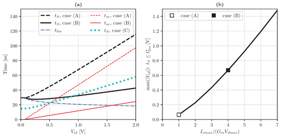
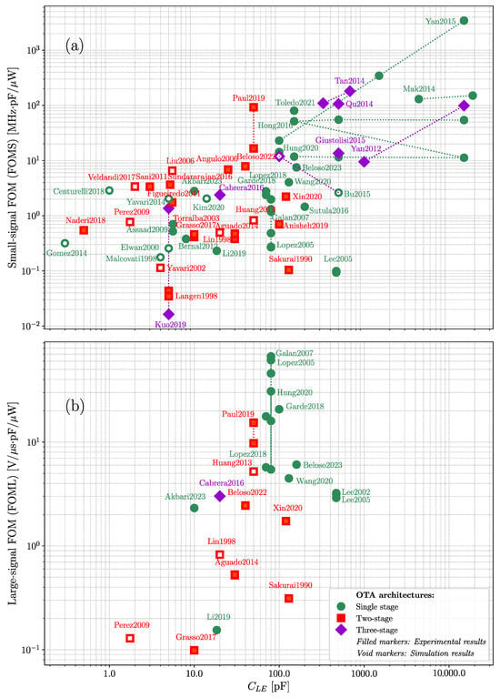
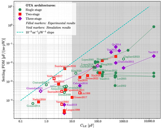
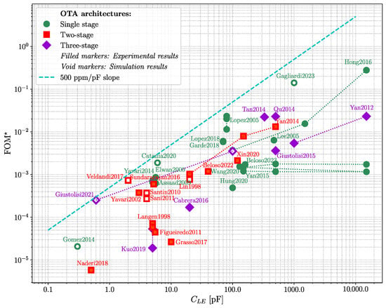
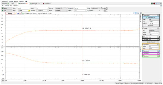
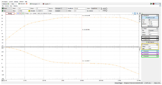
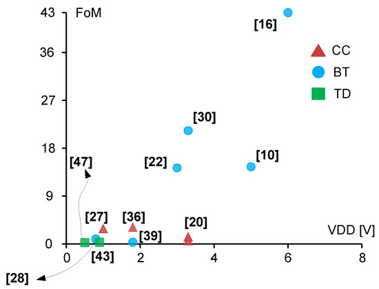
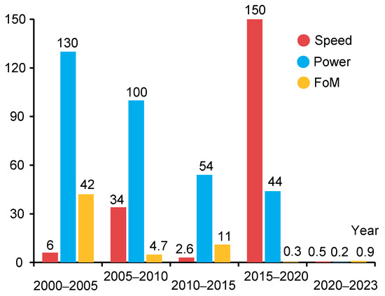
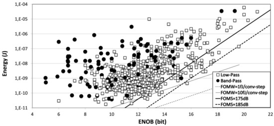
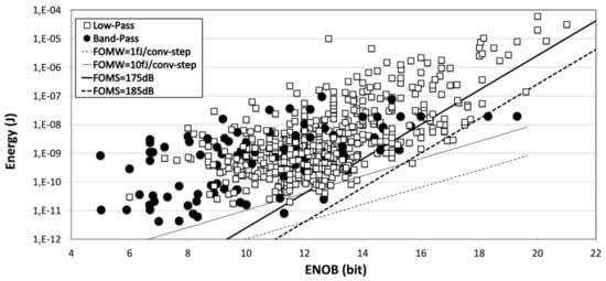
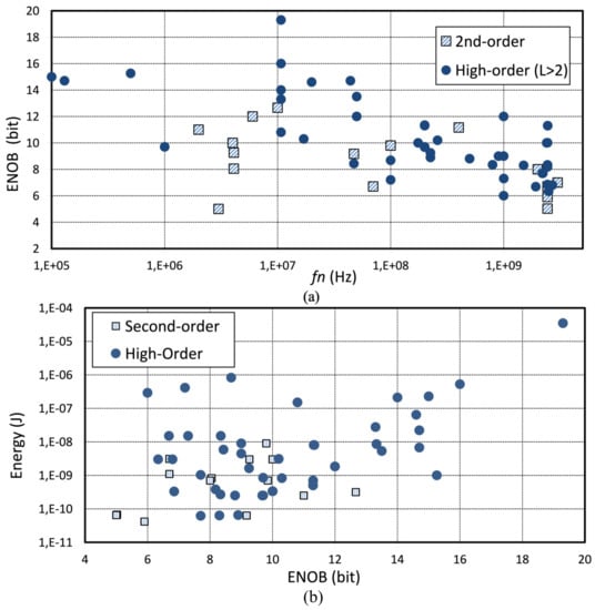
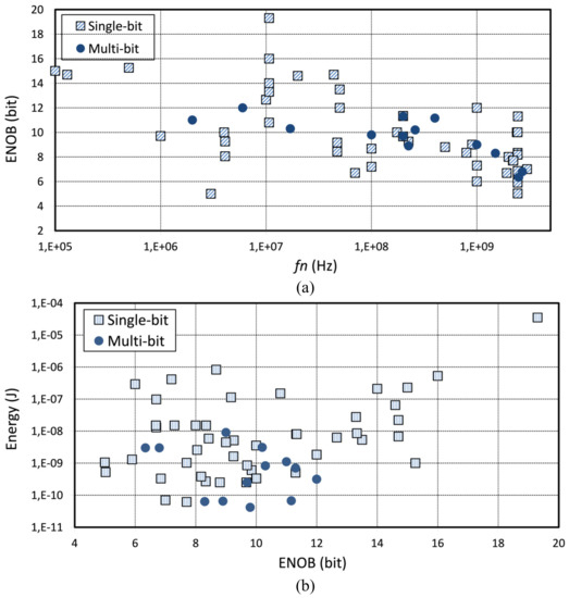
This review is aimed at the integrated circuit design community and it explores slew-rate enhancement techniques for switched-capacitor amplifiers, with a primary focus on optimizing settling time within power constraints. Key challenges are addressed, including the selection between single-stage and two-stage amplifiers, along with the utilization of advanced circuit-level techniques for slew-rate enhancement. Presently, there exists a gap in comprehensive discussion, with reliance primarily on two Figures of Merit aimed at assessing power efficiency under specific capacitive loads. However, these metrics fail to adequately assess the performance of the existing slew-rate enhancer solutions at different values of capacitive loads. As a consequence, the designer lacks clear guidelines in practical situations. This review provides a state-of-the art mapping under a figure of merit dedicated to assess the whole settling delay, and also introduces a novel performance metric which highlights the role of the circuital architectures, regardless of external operating conditions. By offering a thorough examination, this review seeks to steer future research in switched-capacitor amplifier design, thereby facilitating informed decision-making and fostering innovation in the field.
Full article
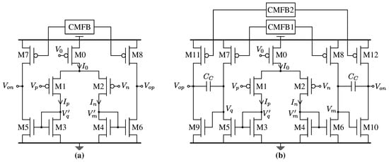
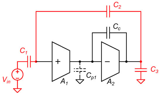
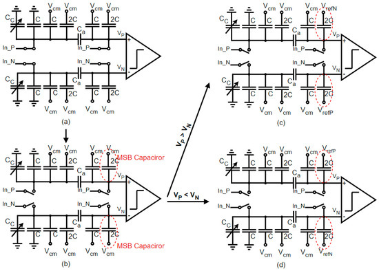
Figure 1


