Article

On-Chip Adaptive Implementation of Neuromorphic Spiking Sensory Systems with Self-X Capabilities

1
Department of Electrical and Computer Engineering, Institute of Cognitive Integrated Sensor Systems (KISE), RPTU Kaiserslautern-Landau, 67663 Kaiserslautern, Germany
2
College of Electronics Engineering, Ninevah University, Ninevah 41002, Iraq
*
Author to whom correspondence should be addressed.
Current address: KISE, Erwin-Schrödinger-Strasse, Gebäude 12, 67663 Kaiserslautern, Germany.
Chips 2023, 2(2), 142-158; https://doi.org/10.3390/chips2020009
Submission received: 3 April 2023 / Revised: 17 May 2023 / Accepted: 2 June 2023 / Published: 6 June 2023

Abstract

:
In contemporary devices, the number and diversity of sensors is increasing, thus, requiring both efficient and robust interfacing to the sensors. Implementing the interfacing systems in advanced integration technologies faces numerous issues due to manufacturing deviations, signal swings, noise, etc. The interface sensor designers escape to the time domain and digital design techniques to handle these challenges. Biology gives examples of efficient machines that have vastly outperformed conventional technology. This work pursues a neuromorphic spiking sensory system design with the same efficient style as biology. Our chip, that comprises the essential elements of the adaptive neuromorphic spiking sensory system, such as the neuron, synapse, adaptive coincidence detection (ACD), and self-adaptive spike-to-rank coding (SA-SRC), was manufactured in XFAB CMOS 0.35 μ m technology via EUROPRACTICE. The main emphasis of this paper is to present the measurement outcomes of the SA-SRC on-chip, evaluating the efficacy of its adaptation scheme, and assessing its capability to produce spike orders that correspond to the temporal difference between the two spikes received at its inputs. The SA-SRC plays a crucial role in performing the primary function of the adaptive neuromorphic spiking sensory system. The measurement results of the chip confirm the simulation results of our previous work.

1. Introduction

The progress in integration technologies on the one hand has facilitated using sensors and sensor systems, on the other hand it has aggravated the design of the corresponding electronics. The utilization of cutting-edge technologies in implementing mixed-signal systems offers power and speed gains, as stated in [1]. This is primarily attributed to the reduced capacitance value and lower supply voltage. However, to interface efficiently with an expanding range of sensors, sensor systems must possess highly accurate, robust, and flexible analog front-ends with self-X (self-calibration, self-trimming, self-optimization, and self-healing) properties. Developing dependable AFEs is paramount to the overall success of the application system. In contemporary cutting-edge integration technologies, the conventional analog design that relies on amplitude-domain information representation encounters progressively harder-to-surmount obstacles. As mentioned in [2], circuit design encounters numerous challenges, such as reduced intrinsic device gain, noise, aggravated device mismatch, lower supply voltage, decreased signal swing, and manufacturing deviations. When transitioning to smaller technologies, these challenges complicate signal processing in the amplitude domain, particularly for complex mixed-signal systems such as ADC [1,2,3,4].
State-of-the-art designs aim to tackle the challenges associated with analog-to-digital converters (ADCs); various structures have been proposed in the literature. An instance of this is the synthesizable stochastic flash ADC architecture, which necessitates a significant amount of resources to execute, such as 3840 comparators to achieve 5.3 bits of resolution [1,2]. In [5], the researchers suggested a structure for a 4-bit ADC that uses memristors, along with a trainable artificial neural network (ANN) calibration. This design aims to minimize inaccuracies caused by device mismatch and allow the circuit to adapt to environmental changes. As well, the authors of [6,7] introduced a synthesizable ADC that draws inspiration from a neural network. This ADC utilizes the crossbar architecture of resistive random-access memory (RRAM) in a dual-path setup. The architecture of the ADC comprises three layers of hardware substrate for a general neural network: the input layer, the hidden layer, and the output layer.
Nevertheless, the ADCs in [1,2,5,6,7] employ amplitude-coded signals that encounter difficulties in modern node CMOS technology. In contrast, the gate delay in digital circuits is reduced by scaling the transistor dimension and supply voltage in CMOS technology. As a result, the time resolution improves with CMOS scaling, leading to a growing interest in the time domain, as reported by [8,9]. This motivated the researchers to create electronic sensor systems that use spike or time-coded signals, which possess a technology-agnostic property that remains robust even as technology scales up, as demonstrated in [10,11,12,13,14,15]. A scalable ADC based on the neural engineering framework was proposed by the authors in [10]. This approach leverages the inherent parallelism of neural networks by designing the encoder and neurons in the analog domain, and implementing the decoding and signal reconstruction in the digital domain. Furthermore, an ADC-based current sensing model [12] utilizes the Izhikevich neuron model to implement a current-to-frequency converter, while digital blocks are used to implement frequency-to-digital conversion in its architecture. The process of translating analog input values into input pulse frequencies through a large number of spikes can result in increased power consumption as the spiking neural network (SNN) structure grows deeper and larger. Consequently, these traits may not be well-suited for power-efficient and robust devices in edge computing [13,15].
In order to address these obstacles, a previous design of the sensor to spike to digital converter (SSDC α ) chip utilized spike timing to simulate acoustic localization [11]. However, it did not incorporate adaptivity, which is essential for maintaining system functionality in the face of drift, aging, lesions, or damage. The ability to create an accurate, robust, and adaptable design is crucial for the overall application system’s success. Consequently, we have integrated the essential blocks of our proposed neuromorphic spiking sensory system that possesses self-X properties and utilizes either spike or time-coded signals in our chip [16]. This system was designed with a technology-agnostic feature that remains resilient even with technology scaling. This adaptive approach carries the promise to compensate both static and dynamic degradations, reversible and irreversible ones in both cases. In earlier work [17,18,19,20], the concept of using spike timing was introduced, to convey information and emulate acoustic localization.

2. Inspirations from Biological Sensory Systems

Living organisms utilize interaural time differences (ITDs), which refers to the time delay between signals reaching the two ears, to determine the location of a sound source. In 1948, Jeffress introduced the concept of acoustic localization [21], which is grounded on three fundamental principles: delay lines, coincidence detectors, and place map [22]. Figure 1a displays a distinct adaptive spiking neural network (SNN) model for acoustic localization. In Figure 1b, we present a neuromorphic spiking sensory system that integrates adaptation features in a two-stage configuration, which emulates Jeffress’s model [21]. In the first stage, the sensor signal-to-spike converter (SSC) converts the sensor signal into two spikes that vary in time difference (TD) based on the sensor signal. The early work conducted initial research on a CMOS image sensor that utilized a light-to-frequency or light-to-spike-code converter, with a focus on high dynamic range imaging [23]. In subsequent studies, researchers expanded upon the concept by incorporating additional sensor modalities and exploring the time to the first spike coding [11]. Furthermore, they explored its application to differential representation using the Wheatstone bridge sensor, for example, in the case of xMR sensors. The technologies known as giant magnetoresistance (GMR) and tunnel magnetoresistance (TMR) have emerged and are collectively referred to as xMR. The second stage, the self-adaptive spike-to-digital converter (SA-SDC), generates a digital code corresponding to the TD value. The three core principles of Jeffress’s theory are integrated into the SA-SDC through synapse weights, an array of adaptable coincidence detection, and a winner-takes-all (WTA) mechanism with memory [18].
In our chip, we addressed the aforementioned issues by making two contributions to the universal-sensor-interface with self-X properties (USIX), as described in our earlier publication [16]. The multi-project-chip (MPC) USIX is named as such because we integrated the fundamental blocks of contributions based on amplitude- and spike-domain representation with self-X for analog front-ends (AFE). The first contribution pertains to reconfigurable hardware, and its outcomes have already been published in [24]. This paper aims to complement the spiking part using the chip and measurement results of the second contribution in section four of the previous paper [16]. Figure 2a displays the chip layout implementation, while Figure 2b shows the specifics of the post-manufacturing chip that incorporates the essential components of the adaptive neuromorphic spiking sensory system, including neurons, synapses, adaptive coincidence detection (ACD), and SA-SRC. Due to the passivation coating and the top metal layer applied to the chip, the details of the die surface are not visible. The main objective of this project is to perform a test on the essential component of our proposed neuromorphic spiking sensory system, which is SA-SRC, using our chip.

3. Proposed Methodology

There has been a surge in demand for sensor systems in Industry 4.0 and IoT that can effectively operate in a dynamic environment and tackle the limitations of conventional sensor systems in the amplitude domain. The aim of this project is to create an innovative neuromorphic spiking sensory system that possesses self-X capabilities, which exhibits several promising features such as low-voltage operation, noise-robust conditioning, and low power consumption, overcoming the technology scaling issues. The neuromorphic spiking sensory system transmits information through spike time, making it suitable for implementation in advanced sensory electronic systems with high reliability using cutting-edge technologies. The proposed neuromorphic spiking sensory system consists of SSC and SA-SDC, as illustrated in Figure 1.

3.1. Sensor Signal-to-Spike Converter (SSC)

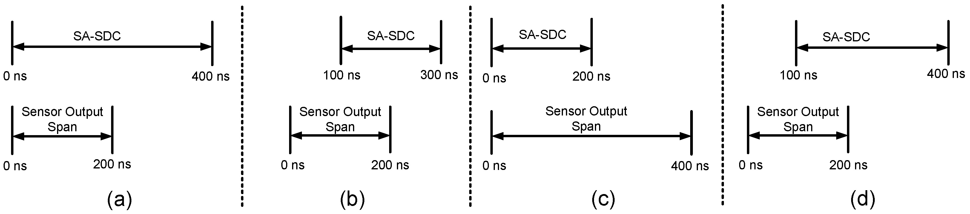
The sensor output span seldom equals the input span of the SA-SDC, as shown in Figure 3, and if the sensor span is smaller than the input span of the SA-SDC, as shown in Figure 3a, the dynamic range of the SA-SDC is not fully utilized; it will not make use of all ACDs. Furthermore, the spans of the sensor and SA-SDC may be equal, but they are offset, as shown in Figure 3b. On the other side of the sensor, if the span is greater than the input range of the SA-SDC, as shown in Figure 3c, then sensor data is lost. In another case, there is a difference in both duration (200 ns and 300 ns) and offset (100 ns) of the spans, as illustrated in Figure 3d. Often the spans are offset and unequal. Therefore, amplification and level shifting in the time domain are needed to match the spans. The mismatched spans require an expensive increase in the SA-SDC dynamic range or loss of sensor data; therefore, the spans of the sensor and SA-SDC must be matched to obtain optimum performance. The SSC is a conditioning circuit that matches the sensor and SA-SDC, making the spans equal without a level shift. The SSC is so versatile that it amplifies and level shifts in the time domain of the sensor signal simultaneously. In the next step of the design, we will develop an SSC unit, which is required for the proposed project.

3.2. Self-Adaptive Spike-to-Digital Converter (SA-SDC)

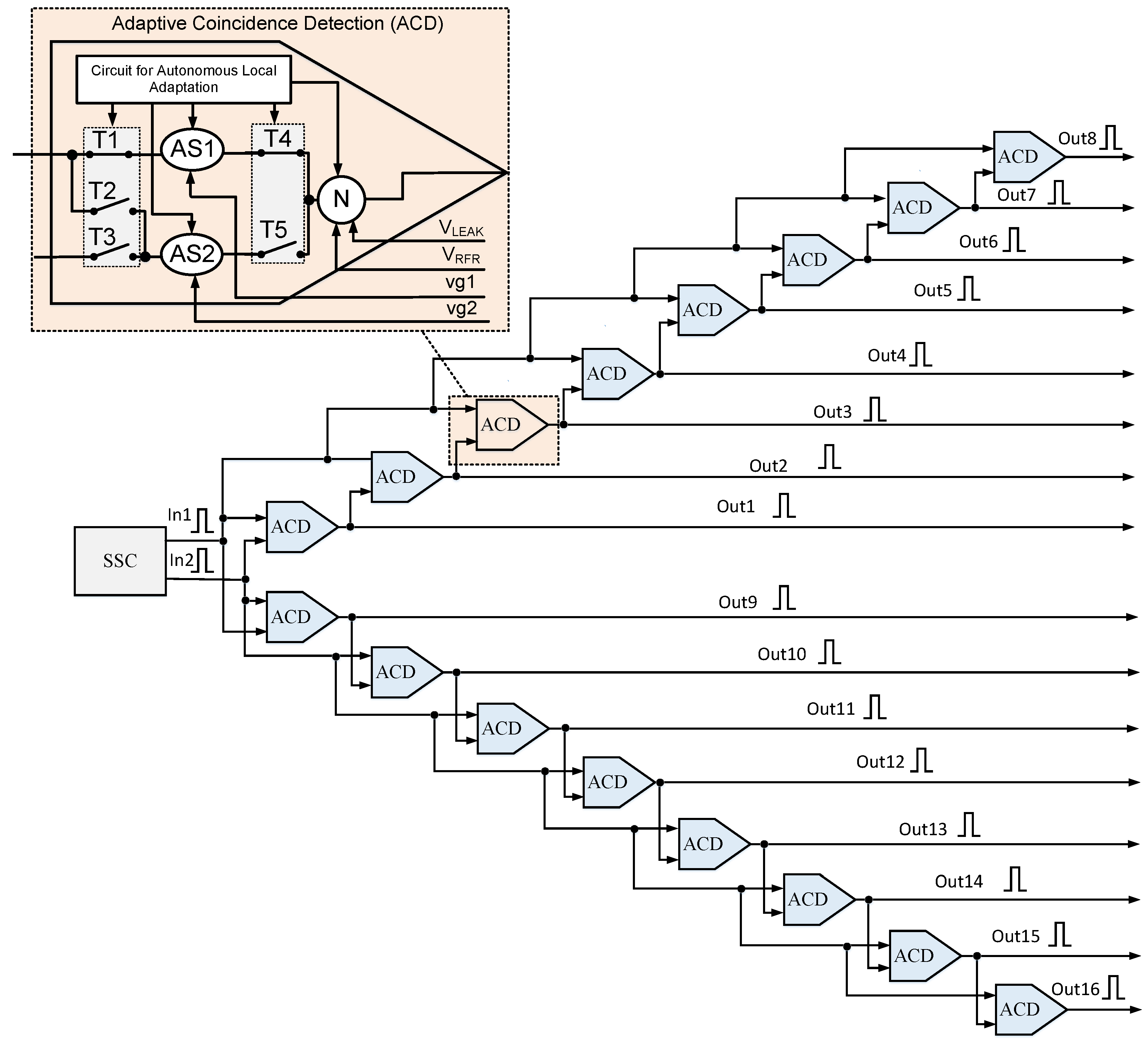
The SA-SDC that is being proposed consists of two components, the first being the self-adaptive spike-to-rank coding (SA-SRC) and the second being the winner-take-all (WTA) mechanism that incorporates memory, as illustrated in Figure 1. The SA-SRC has a tendency to produce spike orders that correspond to the time difference between two spikes received at its inputs. Spike order codes are a type of coding method that relies on the arrangement of spikes across a group of neurons, which is determined by the firing sequence of those neurons [25,26]. The rank order code is converted into digital numbers through the second component, WTA. By adding more ACDs in a cascade, the ability to measure time intervals between in1 and in2 can be enhanced, resulting in an increased resolution of the SA-SDC. The number of ACDs needed to achieve a specific number of bits (NOB) can be determined using Equation (1), which was developed in [18].
NOB = l d ( x )
where x is the number of ACDs. Sixteen adaptive coincidence detection (ACD) units are employed to implement the proposed SA-SRC for the current stage of the development, as shown in 
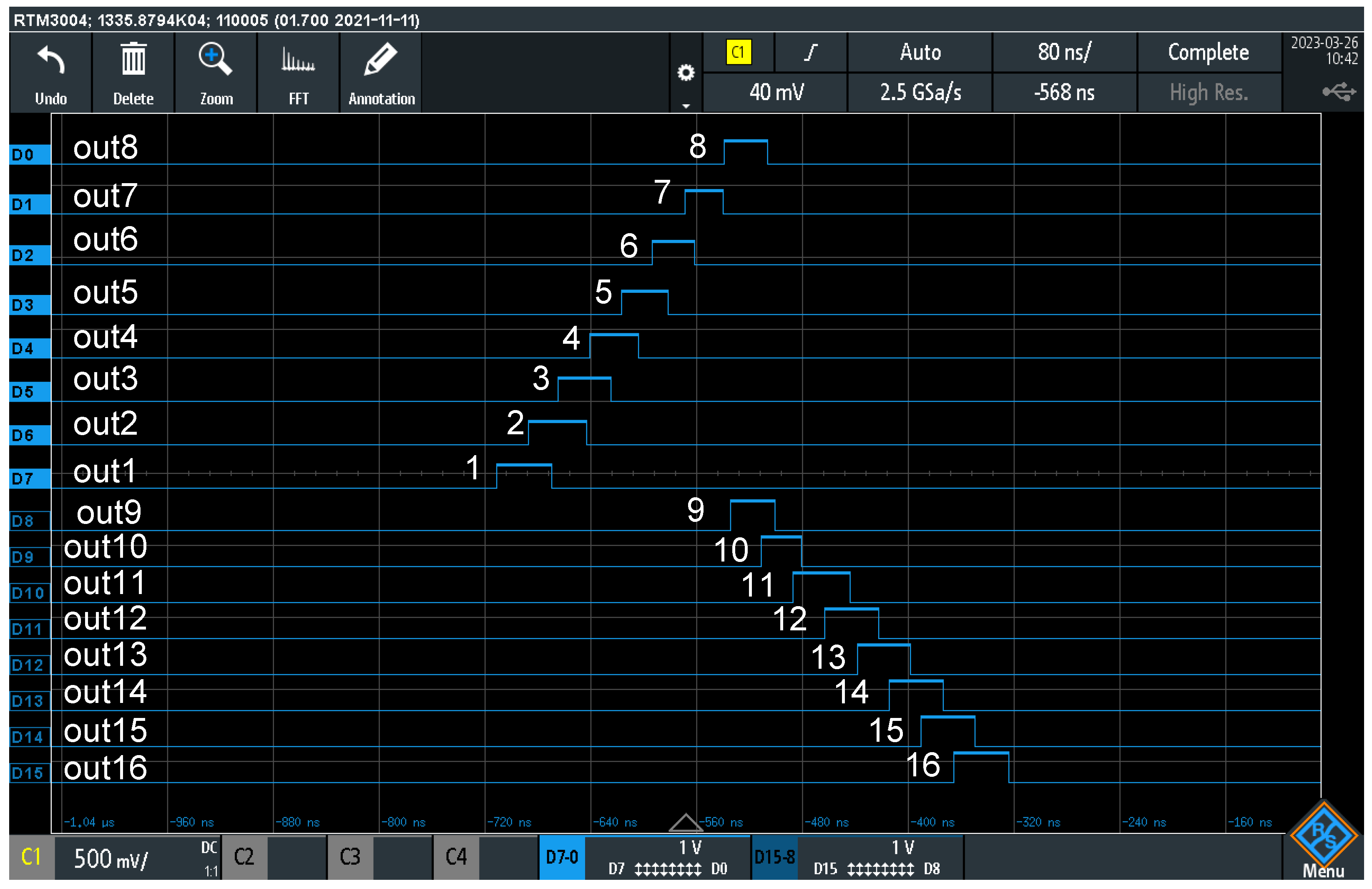
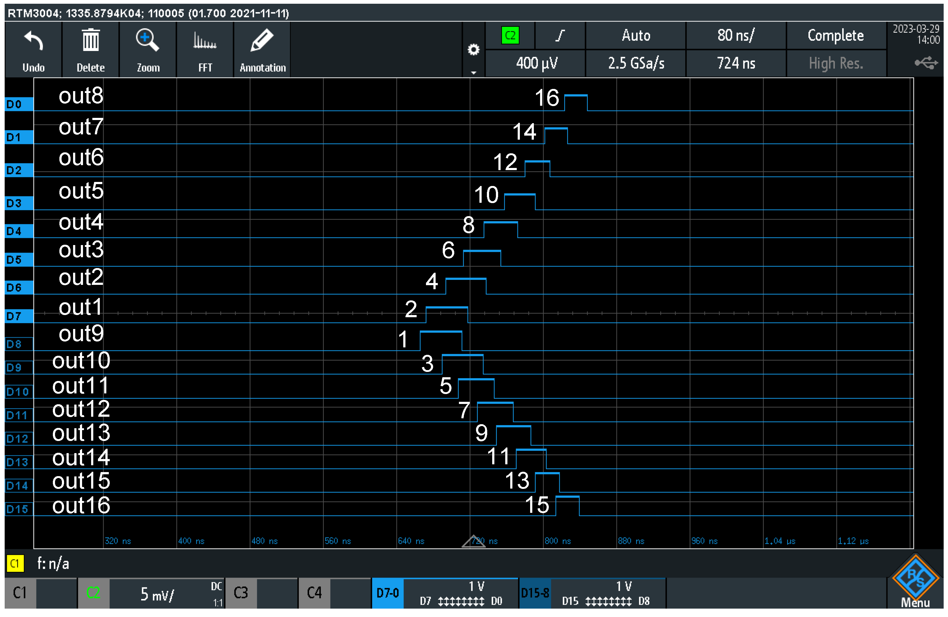
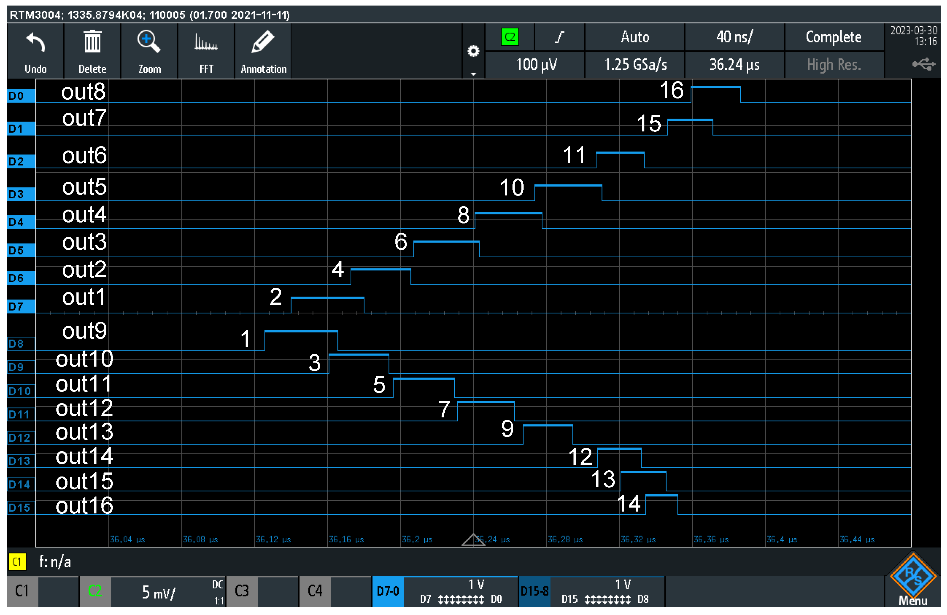
Figure 4. The NOB can be calculated by using Equation (1), which yields a result of 4 bits. The SA-SRC consists of two symmetrical sections, specifically the upper and lower parts, which generate the SA-SRC outputs from Out1 to Out8 and Out9 to Out16, respectively. Therefore, the presented concept can work for both single-ended and differential or difference sensorial input, the current implementation uses (spike time) difference input. This system is equipped with two inputs, referred to as in1 and in2. In the upper section, input in1 is linked straight to the first input of the ACDs. On the other hand, the input in2 is transmitted through the ACDs sequentially, representing the delay chains of the upper section. In contrast, in the lower section, input in2 is directly connected to the first input of the ACDs, while input in1 is transmitted through the ACDs one by one, representing the delay chains of the lower section. The duration of the delay chain unit depends on when the neuron fires, which is influenced by the amount of input current it receives. However, the input current to the neuron is adjusted by the synapse weight. As a result, the weights of the synapses adjust to the delay of each unit in the chain, even when there are variations.
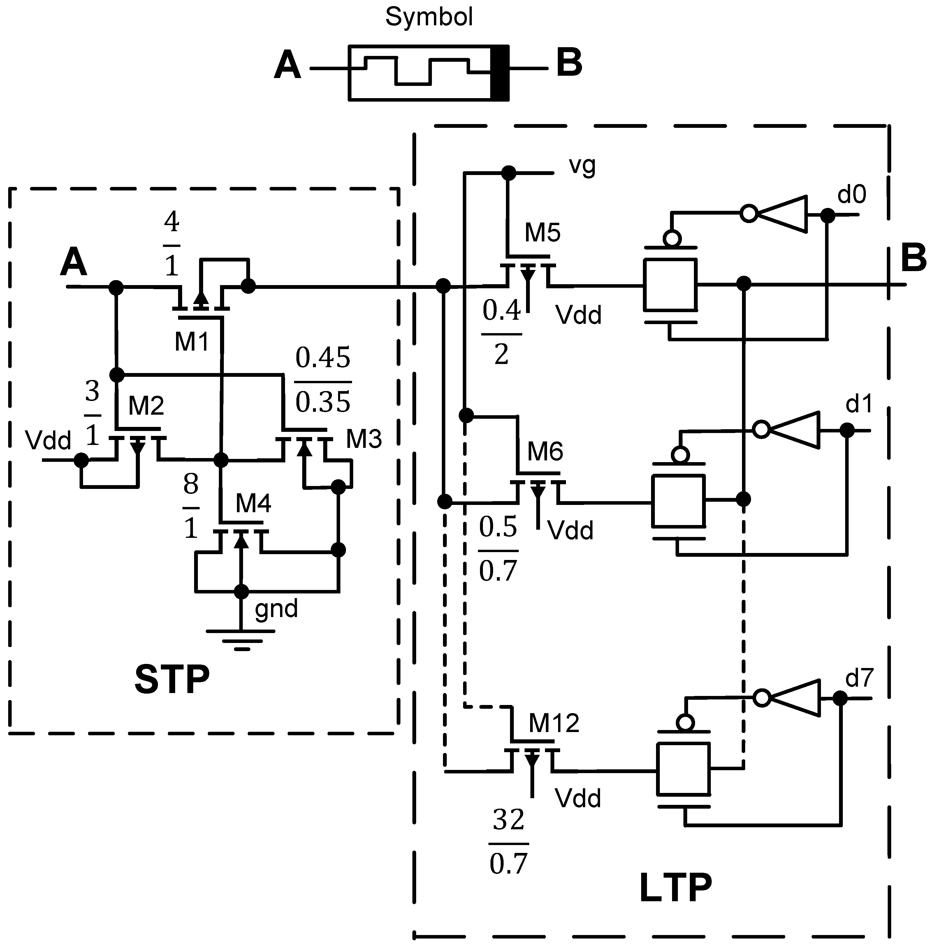
Each ACD unit consists of one neuron (N) and two adaptive synapses (AS). In [18], we suggested an adaptive synapse that utilizes the CMOS memristor to imitate the short-term plasticity (STP) and long-term plasticity (LTP) of a biological synapse. 
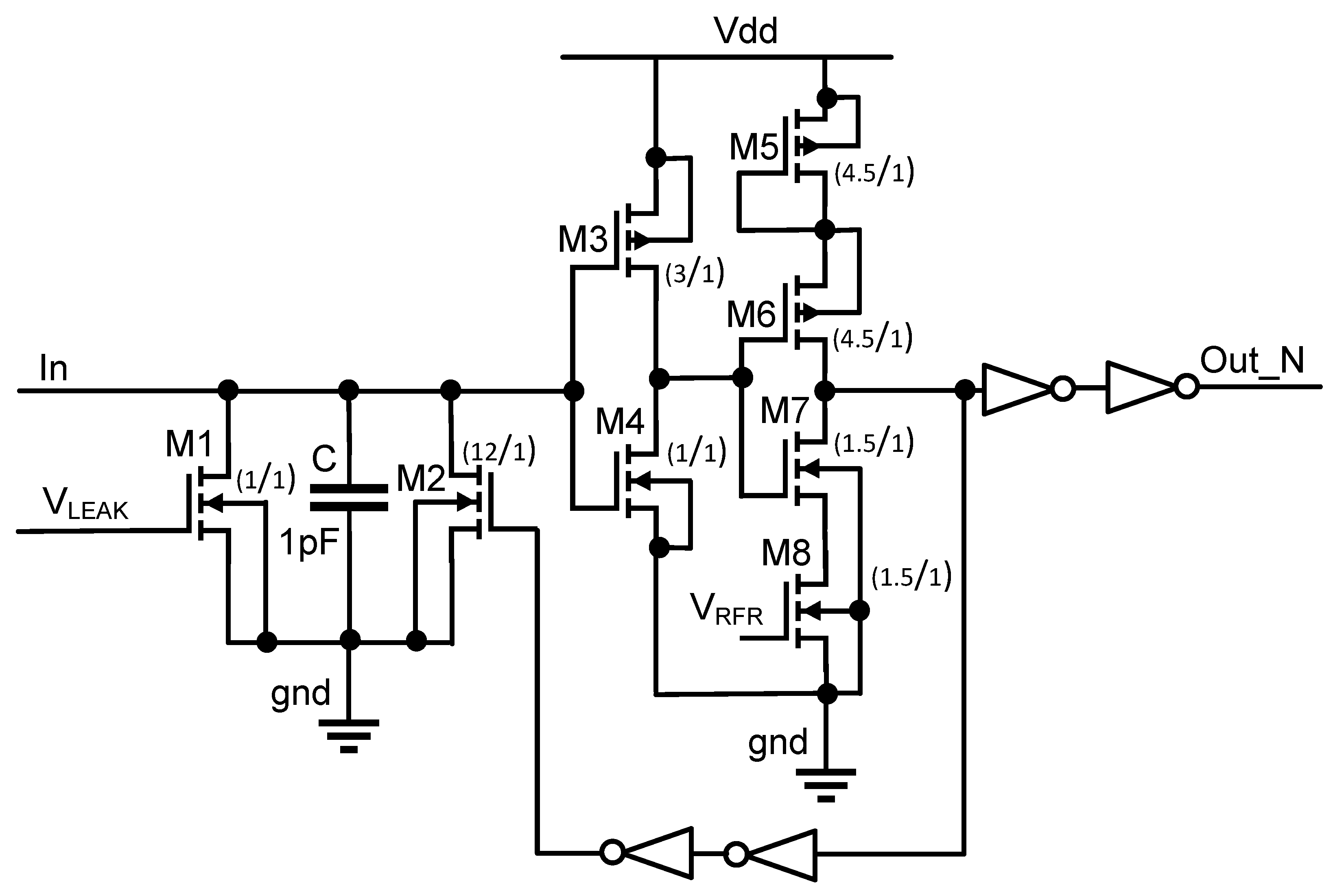
Figure 5 displays the schematic of the adaptive synapse we proposed.
Indiveri’s neuron model, known as the leaky integrate and fire (LIF) neuron model, includes various components that allow for setting an arbitrary refractory period, spike frequency adaptation, positive feedback, modulating the neuron’s threshold voltage, membrane capacitor, a transistor for controlling the current leakage, and a digital inverter for pulse generation [27]. The essential characteristics necessary for the ACD involve the ability of neurons to implement time delays in a neural network, along with an inverse correlation between the magnitude of incoming charges and the timing of the first spike. These properties are inherent in any neural spiking model. We modified the Indiveri neuron model in [16] to fulfill the needs of ACD and enhance power efficiency, area utilization, and processing speed. A schematic of the modified neuron model can be observed in Figure 6.
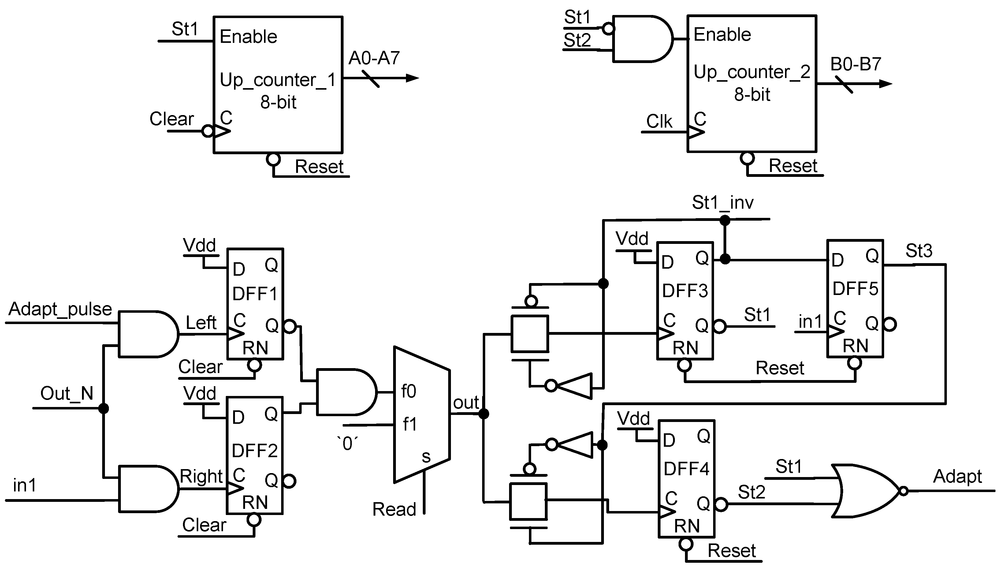
There are two modes of operation for the ASRC. The first is the normal mode, in which both synapses of the ACD are connected to the neuron. The second mode is the adaptation mode, which was created in [18] by implementing a two-layer adaptation hierarchy. The first layer operates at the ACD level, while the second layer operates at the SA-SRC level. The first layer is entirely self-adaptive and local, operating in an unsupervised manner. In the first layer, the weight of a synapse is determined by the timing of neuron firing, which is based on the input current it receives. This approach depends on the fact that the timing of neuron firing is affected by the input current, and the weight of the synapse regulates this current. Consequently, the weight of the synapse is directly proportional to the timing of the neuron’s firing. We created a self-adaptive method for the first layer of the ACD by designing an autonomous control circuit, as illustrated in Figure 7 in [
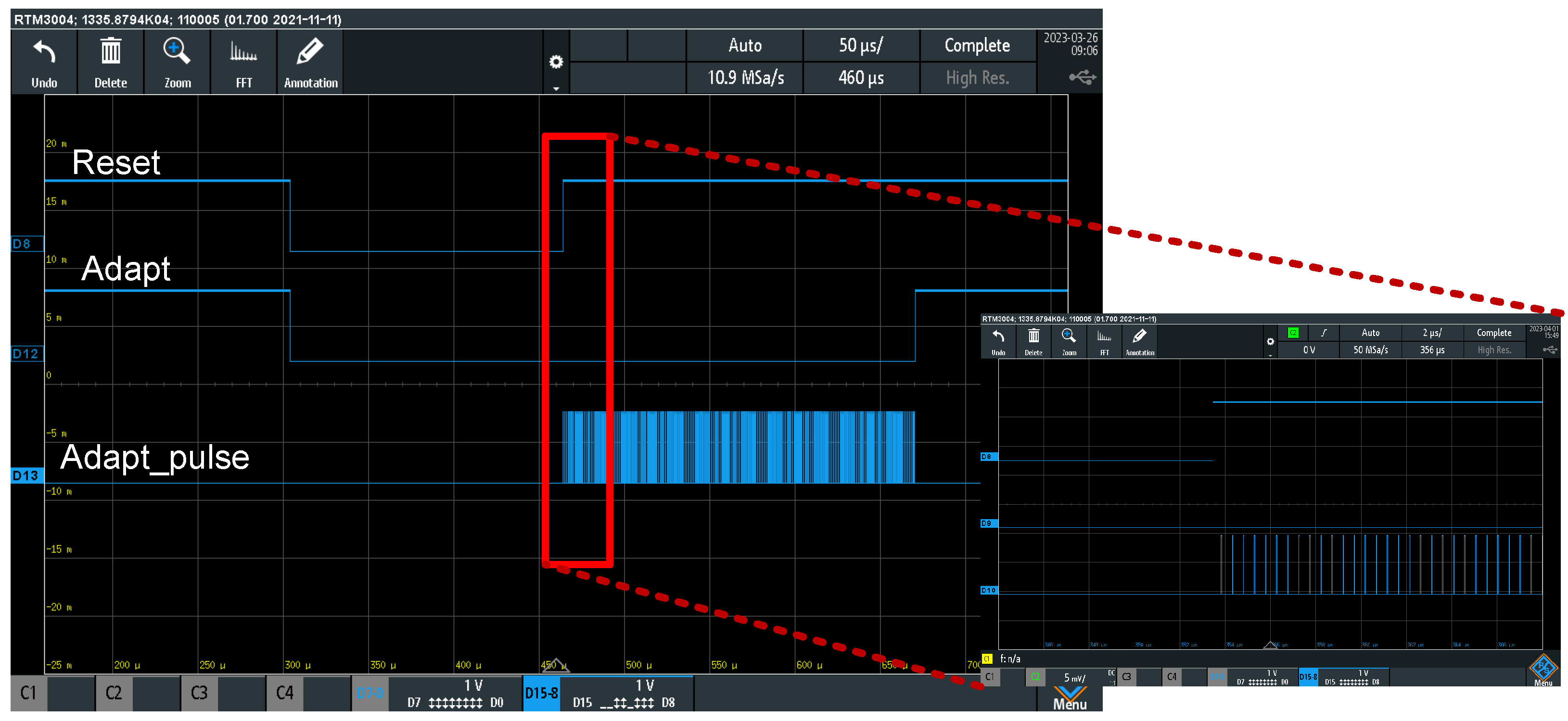
18]. This adaptivity is facilitated through the reset, adapt_pulse, and adapt I/O pins of the SA-SRC. Upon receiving the reset signal, the SA-SRC enters the adaptation mode and sets the adapt output to one upon completion of the unsupervised adaptation of the first level. The SA-SRC utilizes the pulse of the adapt_pulse input to adapt itself. Once the adaptation process is complete, the SA-SRC returns to normal mode, during which it can receive input pulses on its two inputs (in1 and in2), and adjust the output code based on the time difference between them.
The adaptation process in the first level occurs simultaneously for all ACDs through the control of switches T1, T2, T3, T4, and T5, as shown in Figure 4. As a result, the time required for adaptation will not increase with the number of synapses since all synapses are adjusted simultaneously. The weight of the first synapse in all ACDs is adapted simultaneously by the autonomous circuit, achieved by connecting the first synapse while disconnecting the second synapse. Likewise, the weight of the second synapse is also adapted. The maximum adaptation time is determined by multiplying the maximum number of steps by the duration of adapt_pulse. According to [18] (p. 246), our adaptation scheme allows for a maximum of 512 steps. The actual adaptation time will be influenced by process, voltage, and temperature (PVT) conditions. Upon powering-up the MPC USIX chip, all weights are initially set to zero, and the weight corresponds to the delay. The process of adaptation starts from scratch and progresses until the desired synapse weight is achieved, resulting in uniform delays across all connections.
The second level of adaptation operates above the first level and is responsible for adjusting the variables vg1, vg2, V LEAK , and V RFR . This level operates above the first level and waits for the first level to complete its solution after every modification to these variables. If the solution successfully corrects the synapse weight, the adaptation process ends. If not, the second level updates the variables (vg1, vg2, V LEAK , and V RFR ) and initiates adaptation for the next round. At present, these four variables are being manually adjusted in the current stage of development of our design.

4. Experimental Setup

A shipment of 32 packaged chips was received from the XFAB foundry. For the current investigation, only chip number four was analyzed, while the remaining chips will be examined in a subsequent step. The FPGA evaluation board from Red Pitaya was selected as the edge computing device for the demonstration prototyping to evaluate the essential components of the adaptive neuromorphic spiking sensory system at the physical hardware level. An appropriate PCB with a socket extended the Red Pitaya system to complete the demonstration board, which could then be used to explore the essential neuromorphic spiking sensory system blocks such as a neuron, synapse, ACD, and SA-SRC on the MPC USIX chip, as shown in Figure 8.
Using the Verilog hardware descriptive language, we developed a control module on the programmable logic (PL) present in the Red Pitaya, as shown in Figure 9. This control module has the responsibility of overseeing the reset, adapt_pulse, and adapt I/O pins of the SA-SRC cell. Additionally, it generates two input pulse with time differences for the in1 and in2 of the SA-SRC. The control module utilizes the general-purpose I/O pins present on the Red Pitaya to establish a direct interface with the I/O pins of the SA-SRC cell on the MPC USIX chip.
In the second level, there are four variables, namely, vg1, vg2, V LEAK , and V RFR . These variables have been manually adapted in the current stage of our design development. Initially, their values were determined based on empirical results and observations from measurement results, as illustrated in Table 1.

5. Experimental Results

In this experiment, we investigated the properties of the SA-SRC cell and its ability to adapt on a manufactured chip. The adaptation process of the first level is illustrated in [18] (p. 243, Figure 11) and begins with resetting the SA-SRC. Once the reset signal returns to one, the SA-SRC adapts using a pulse signal called adapt_pulse, as depicted in Figure 10. The output signal, adapt, indicates whether the SA-SRC is undergoing self-adaptation or not, with a value of 0 indicating that it is. The adaptation of weights is accomplished through the input pulse adapt_pulse, operating at a frequency of 2 MHz. Therefore, the time of one step is 500 ns. During the experiment, the adaptation time and the number of steps taken by the SA-SRC were recorded, and at a room temperature of 22 °C, the measurements were 210 μ s for adaptation time and 420 steps.
According to the experimental findings, the SA-SRC cell has the ability to produce 16 distinct spike order codes that correspond to the time difference values between its input signals. The time difference (TD) between in1 and in2 ranges from −120 to 120 ns, in increments of 15 ns, which is equivalent to a 4-bit binary code, as the experiment results in Table 2 and Table 3 show. In the current experiment, we emulated the first block of our proposed system, SSC, by utilizing the programmable logic (PL) available in the Red Pitaya. The input of the SA-SRC block is fed by two outputs, in1 and in2, from the SSC that is emulated in Red Pitaya. Consequently, the time difference between in1 and in2 was constrained by the capabilities of the Red Pitaya board. As a result, instead of the expected steps of the time difference (15 ns, 30 ns, 45 ns, and so on until 120 ns), we obtained time steps as listed in Table 2 and Table 3. However, this limitation will not persist when we implement the SSC block in our future work. The experiment results presented in Figure 11 and Figure 12 demonstrate that the SA-SRC generates different codes for each value of TD when two pulses with different TD values are applied to its input. The SA-SRC outputs, labeled out1 to out16, represent the one spike order code, and the numbers indicated on the output waveforms represent the sequence of the spike order relative to the other outputs. Figure 11 depicts the instance where in2 comes before in1 within a time difference of 120 ns. On the other hand, Figure 12 exhibits the opposite scenario, where in1 comes before in2 within a time difference of 15 ns. The rank codes were decoded using the algorithm conceived in [18] (p. 253). The SA-SRC’s operational capability is demonstrated under varying voltages. The output spike orders are observed to fluctuate as the power supply changes from 3.3 V to 3 V, as depicted in Figure 13 and Table 4. The automatic adaptation mechanism of the first layer compensates for these variations, resulting in the output spike orders being reset to their initial states, as illustrated in Figure 12 and Table 4. Through the time of the experiment, the SA-SRC’s adaptation time and the number of steps it took were documented. At a room temperature of 22 °C, the results showed an adaptation time of 225 μ s and 450 steps. The capacity of SA-SRC to counteract process and voltage fluctuations has been confirmed by the measurement results. The chip’s measurement results have verified our previous work’s simulation results. Table 5 illustrates the comprehensive comparisons between the state-of-the-art approaches and the findings presented in this work.

6. Conclusions

Having sensors and appropriate sensor electronics that connect an application system to the physical world is crucial for its overall success. Therefore, our objective was to create an adaptive neuromorphic spiking sensory system that boasts several advantageous features, such as resilience to noise, efficient power usage, compatibility with technology scaling, and low-voltage operation. The information representation method is based on the pulse or spike domain, which draws significant inspiration from biological sensor systems. This work aims to supplement the measurement results of the adaptive implementation of a neuromorphic spiking sensory system using a chip. Our chip, which includes the fundamental components of the adaptive neuromorphic spiking sensory system, namely, the neuron, synapse, ACD, and SA-SRC, was manufactured in XFAB CMOS 0.35 μ m technology via EUROPRACTICE. The main emphasis of this paper is on the measurement outcomes of the SA-SRC, which is responsible for carrying out the primary functionality of the adaptive neuromorphic spiking sensory system. In this work, we examined the effectiveness of its adaptation method and appraised its ability to generate spike sequences that reflect the time difference between the two input spikes. The SA-SRC cell’s first level of adaptivity is described, which operates in an unsupervised manner and is completely self-adaptive and local. The measurement outcome of this initial layer of the adaptation hierarchy is presented. The operational capability of the SA-SRC is demonstrated to withstand voltage variations. The output spikes’ magnitudes change in response to voltage fluctuations, but the adaptation mechanism resets them to their original levels. The adaptation time of the first-level SA-SRC was measured, and it was 210 μ s. The fabricated SA-SRC cell can produce 16 unique output spike orders, corresponding to a 4-bit resolution. Regarding energy consumption, the SA-SRC cell utilizes 297 μ w of energy. In terms of speed, the conversion time for the SA-SRC is 370 ns. The selection of the 0.35 μ m technology and the 4-bit version for implementation was driven by cost considerations and aimed to demonstrate the feasibility of the solution. However, it should be noted that the concept is not limited to these parameters and can be scaled up in terms of both bit capacity and technology used. Table 5 presents a thorough comparison between the findings presented in this work and the state-of-the-art approaches. Finally, the simulation results of our previous work were confirmed by the experiment’s results on the MPC USIX chip presented in this paper. In future work, we will present the measurement outcomes of the other cells of our chip, neuron, synapse, and ACD. Furthermore, we will develop an SSC unit which is essential for the presented work. In the presented investigation, we have only utilized one chip out of our 32 packaged chips. We will investigate the adaptation for the complete batch of chips under static and dynamic variations, e.g., temperature. The ADC standard characteristics such as INL, DNL, and SNR will be measured next.

Author Contributions

Conceptualization, A.K. and H.A.; methodology, A.K. and H.A.; software, H.A.; validation, H.A.; formal analysis, H.A.; investigation, H.A.; data curation, H.A.; writing—original draft preparation, A.K. and H.A.; writing—review and editing, A.K. and H.A.; visualization, H.A.; supervision, A.K.; project administration, A.K. All authors have read and agreed to the published version of the manuscript.

Funding

This research received funding from DAAD by PhD grants.

Institutional Review Board Statement

Not applicable.

Informed Consent Statement

Not applicable.

Data Availability Statement

Not applicable.

Acknowledgments

The authors would like to thank the DAAD (Deutscher Akademischer Austauschdienst) for sponsoring the PhD researchers. We would also thank EUROPRACTICE for their support in providing design tools and MPW fabrication services for our prototype chip and research activity. The reported work and, in particular, the chip manufacturing, was made possible due to funding from the BMBF (German Federal Ministry of Research), obtained in the context of the programme: SElekt_I40, concluded consortial project: MoSeS-Pro, subproject: ’Robuste adaptive integrierte Sensorelektronik und Informationsverarbeitung mit Self-X-Eigenschaften für zuverlässige Systeme der Industrie 4.0’, grant no. 16ES0425, and is gratefully acknowledged.

Conflicts of Interest

The authors declare no conflict of interest.

Abbreviations

The following abbreviations are used in this manuscript:
AFEAnalog front-ends
USIXUniversal-sensor-interface-with-self-X-properties
AFEXAnalog front-ends with self-X properties
ADCAnalog-to-digital converters
ANNArtificial neural network
RRAMResistive random-access memory
ITDInteraural time differences
WTAWinner-takes-all
MPCMulti-project-chip
GMRGiant magnetoresistance
TMRTunnel magnetoresistance
SSDC α Sensor to spike to digital converter
SSCSensor-to-spike converter
SDCSpike-to-digital converter
TDTime differences
SA-SDCAdaptive spike-to-digital converter
SA-SRCSelf-adaptive spike-to-rank coding
ACDAdaptive coincidence detection
NOBNumber of bits
LIFLeaky integrate and fire
PVTProcess, voltage, and temperature
PCBPrinted circuit board
NUSNonuniform sampling

References

  1. Weaver, S.; Hershberg, B.; Kurahashi, P.; Knierim, D.; Moon, U.K. Stochastic flash analog-to-digital conversion. IEEE Trans. Circuits Syst. Regul. Pap. 2010, 57, 2825–2833. [Google Scholar] [CrossRef]
  2. Weaver, S.; Hershberg, B.; Moon, U.K. Digitally synthesized stochastic flash ADC using only standard digital cells. IEEE Trans. Circuits Syst. Regul. Pap. 2013, 61, 84–91. [Google Scholar] [CrossRef]
  3. Sun, H.; Sobue, K.; Hamashita, K.; Moon, U.K. An oversampling stochastic ADC using VCO-based quantizers. IEEE Trans. Circuits Syst. Regul. Pap. 2018, 65, 4037–4050. [Google Scholar] [CrossRef]
  4. Chen, L.; Tang, X.; Sanyal, A.; Yoon, Y.; Cong, J.; Sun, N. A 0.7-V 0.6-μW 100-kS/s Low-Power SAR ADC With Statistical Estimation-Based Noise Reduction. IEEE J. Solid-State Circuits 2017, 52, 1388–1398. [Google Scholar] [CrossRef]
  5. You, H.; Amirsoleimani, A.; Xu, J.; Azghadi, M.R.; Genov, R. A subranging nonuniform sampling memristive neural network-based analog-to-digital converter. Mem.-Mater. Devices Circuits Syst. 2023, 4, 100038. [Google Scholar] [CrossRef]
  6. Cao, W.; He, X.; Chakrabarti, A.; Zhang, X. NeuADC: Neural network-inspired synthesizable analog-to-digital conversion. IEEE Trans. Comput.-Aided Des. Integr. Circuits Syst. 2019, 39, 1841–1854. [Google Scholar] [CrossRef]
  7. Cao, W.; He, X.; Chakrabarti, A.; Zhang, X. NeuADC: Neural network-inspired RRAM-based synthesizable analog-to-digital conversion with reconfigurable quantization support. In Proceedings of the 2019 Design, Automation & Test in Europe Conference & Exhibition (DATE), Florence, Italy, 25–29 March 2019; pp. 1477–1482. [Google Scholar]
  8. Henzler, S. Time-to-digital converter basics. In Time-to-Digital Converters; Springer: Berlin/Heidelberg, Germany, 2010; pp. 5–18. [Google Scholar]
  9. Zhang, Y.; Zhu, Z. Recent advances and trends in voltage-time domain hybrid ADCs. IEEE Trans. Circuits Syst. II Express Briefs 2022, 69, 2575–2580. [Google Scholar] [CrossRef]
  10. Mayr, C.G.; Partzsch, J.; Noack, M.; Schüffny, R. Configurable analog-digital conversion using the neural engineering framework. Front. Neurosci. 2014, 8, 201. [Google Scholar] [CrossRef] [Green Version]
  11. Kammara, A.; König, A. SSDCα–Inherently robust integrated biomimetic sensor-to-spike-to-digital converter based on peripheral neural ensembles. Tm-Tech. Mess. 2016, 83, 531–542. [Google Scholar] [CrossRef]
  12. Singhal, N.; Santosh, M.; Bose, S.; Karmakar, A. Low-Current Sensing Analog-to-Digital Converter with Tuneable Resolution for Biomedical Applications. IEEE J. Trans. Electr. Electron. Eng. 2021, 16, 1221–1228. [Google Scholar] [CrossRef]
  13. Oh, S.; Lee, S.; Woo, S.Y.; Kwon, D.; Im, J.; Hwang, J.; Bae, J.H.; Park, B.G.; Lee, J.H. Spiking Neural Networks With Time-to-First-Spike Coding Using TFT-Type Synaptic Device Model. IEEE Access 2021, 9, 78098–78107. [Google Scholar] [CrossRef]
  14. Rao, A.; Plank, P.; Wild, A.; Maass, W. A long short-term memory for AI applications in spike-based neuromorphic hardware. Nat. Mach. Intell. 2022, 4, 467–479. [Google Scholar] [CrossRef]
  15. Vogginger, B.; Kreutz, F.; López-Randulfe, J.; Liu, C.; Dietrich, R.; Gonzalez, H.A.; Scholz, D.; Reeb, N.; Auge, D.; Hille, J.; et al. Automotive radar processing with spiking neural networks: Concepts and challenges. Front. Neurosci. 2022, 16, 414. [Google Scholar] [CrossRef] [PubMed]
  16. Alraho, S.; Zaman, Q.; Abd, H.; König, A. Integrated Sensor Electronic Front-Ends with Self-X Capabilities. Chips 2022, 1, 83–120. [Google Scholar] [CrossRef]
  17. Abd, H.; König, A. Adaptive Spiking Sensor System Based on CMOS Memristors Emulating Long and Short-Term Plasticity of Biological Synapses for Industry 4.0 Applications. tm-Tech. Mess. 2021, 88, s114–s119. [Google Scholar] [CrossRef]
  18. Abd, H.; König, A. Design of a CMOS memristor emulator-based, self-adaptive spiking analog-to-digital data conversion as the lowest level of a self-x hierarchy. J. Sens. Sens. Syst. 2022, 11, 233–262. [Google Scholar] [CrossRef]
  19. Abd, H.; König, A. D10. 3 Adaptive Spiking Sensor Electronics Inspired by Biological Nervous System Based on Memristor Emulator for Industry 4.0 Applications. In Proceedings of the SMSI 2021—Sensors and Instrumentation, Virtual Event, 3–6 May 2021; pp. 232–233. [Google Scholar]
  20. Abd, H.; König, A. A Compact Four Transistor CMOS-Design of a Floating Memristor for Adaptive Spiking Neural Networks and Corresponding Self-X Sensor Electronics to Industry 4.0. Tm-Tech. Mess. 2020, 87, s91–s96. [Google Scholar] [CrossRef]
  21. Jeffress, L.A. A place theory of sound localization. J. Comp. Physiol. Psychol. 1948, 41, 35. [Google Scholar] [CrossRef] [PubMed]
  22. Ashida, G.; Carr, C.E. Sound localization: Jeffress and beyond. Curr. Opin. Neurobiol. 2011, 21, 745–751. [Google Scholar] [CrossRef] [Green Version]
  23. Doge, J.; Schonfelder, G.; Streil, G.T.; Konig, A. An HDR CMOS image sensor with spiking pixels, pixel-level ADC, and linear characteristics. IEEE Trans. Circuits Syst. II Analog. Digit. Signal Process. 2002, 49, 155–158. [Google Scholar] [CrossRef]
  24. Zaman, Q.; Alraho, S.; König, A. Low-Cost Indirect Measurements for Power-Efficient In-Field Optimization of Configurable Analog Front-Ends with Self-X Properties: A Hardware Implementation. Chips 2023, 2, 102–129. [Google Scholar] [CrossRef]
  25. Thorpe, S.; Gautrais, J. Rank order coding. In Computational Neuroscience; Springer: Berlin/Heidelberg, Germany, 1998; pp. 113–118. [Google Scholar]
  26. Thorpe, S.; Delorme, A.; Van Rullen, R. Spike-based strategies for rapid processing. Neural Netw. 2001, 14, 715–725. [Google Scholar] [CrossRef] [PubMed]
  27. Indiveri, G. A low-power adaptive integrate-and-fire neuron circuit. In Proceedings of the 2003 International Symposium on Circuits and Systems, ISCAS’03, Bangkok, Thailand, 25–28 May 2003; Volume 4, p. IV. [Google Scholar]
  28. Wang, W.; Li, Z.; Fu, X.; Wang, Y.; Li, Q. Pipelined Memristive Analog-to-Digital Converter With Self-Adaptive Weight Tuning. IEEE J. Emerg. Sel. Top. Circuits Syst. 2022, 12, 913–921. [Google Scholar] [CrossRef]
  29. Cao, W.; Ke, L.; Chakrabarti, A.; Zhang, X. Evaluating neural network-inspired analog-to-digital conversion with low-precision RRAM. IEEE Trans. Comput.-Aided Des. Integr. Circuits Syst. 2020, 40, 808–821. [Google Scholar] [CrossRef]
  30. Singhal, N.; Santosh, M.; Bose, S.; Karmakar, A. Neuromorphic approach based current sensing analog to digital converter for biomedical applications. In Proceedings of the 2020 IEEE 17th India Council International Conference (INDICON), New Delhi, India, 10–13 December 2020; pp. 1–6. [Google Scholar]
Figure 1. (a) Acoustic localization model. To determine the location of a voice, the brain relies on the interaural time differences (ITDs) between the signals that reach each ear. These ITDs are calculated as the difference between the arrival times of the voice at the left and right ears, denoted as t1 and t2, respectively. (b) Block diagram of proposed neuromorphic spiking sensory systems.
Chips 02 00009 g001
Figure 2. MPC USIX chip. (a) The chip layout comprises the pad frame as well. (b) The manufactured chip exhibits both the sealing ring and the bonding wires.
Chips 02 00009 g002
Figure 3. An instance of spans that need correction. (a) The sensor’s range is narrower than the input range of the SA-SDC. (b) The sensor and SA-SDC have the same range, but there is an offset between them. (c) The sensor’s range is wider than the input range of the SA-SDC. (d) The sensor and SA-ADC have different ranges and also a positional offset.
Chips 02 00009 g003
Figure 4. The SA-SRC has self-X capabilities that rely on a two-layer adaptivity approach. The first layer is executed through the autonomous circuit of ACD, while the second layer employs V LEAK and V RFR to regulate the neuron and vg1 and vg2 to manage the synapses.
Chips 02 00009 g004
Figure 5. The adaptive synapse (AS) in our proposed circuit, with transistor sizes specified in micrometers, mimics the synaptic plasticity, short-term plasticity (STP), and long-term plasticity (LTP) found in biological synapses using CMOS memristor technology.
Chips 02 00009 g005
Figure 6. The analog leaky integrate-and-fire (LIF) neuron circuit, with transistor sizes indicated in μ m, is proposed for use in implementing the adaptive coincidence detection (ACD) block. This circuit is a simplified version of Indiveri’s neuron, with lean cell, simplified to the specific application’s needs.
Chips 02 00009 g006
Figure 7. The ACD’s autonomous control circuit executes the self-adaptation of the synapses’ weights in the first layer.
Chips 02 00009 g007
Figure 8. Photo of MPC USIX chip test setup based on auxiliary PCB and Red Pitaya.
Chips 02 00009 g008
Figure 9. The flow diagram of the control module on the programmable logic makes use of the general-purpose I/O pins available on the Red Pitaya to create a direct interface with the I/O pins of the SA-SRC cell on the MPC USIX chip.
Chips 02 00009 g009
Figure 10. Measurement results of the adaptation process for the SA-SRC cell on the MPC USIX chip.
Chips 02 00009 g010
Figure 11. The SA-SRC’s measurement results on-chip with in2 preceded by in1 with a difference of 120 ns at a room temperature of 22 °C.
Chips 02 00009 g011
Figure 12. The SA-SRC’s measurement results on-chip with in1 preceded by in2 with a difference of 15 ns at a room temperature of 22 °C.
Chips 02 00009 g012
Figure 13. The measurement results of SA-SRC indicate that the on-chip signal in1 leads in2 with a difference of 15 ns. The sequencing of the output spikes varies with the change in voltage from 3.3 V to 3 V at a room temperature of 22 °C.
Chips 02 00009 g013
Table 1. Second-level variable values at room temperature of 22 °C.
vg1vg2 V LEAK V RFR
2 V2 V0.45 V0.78 V
Table 2. The on-chip SA-SRC measurement outcomes indicate that the output spike sequence of in2 preceded in1 with a time difference ranging from 15 ns to 120 ns at a room temperature of 22 °C.
Time Difference *15 ns32 ns40 ns55 ns70 ns95 ns107 ns120 ns
Binary Output00000001001000110100010101100111
SA-SRC OutputsSpikes Order
out111111111
out232222222
out354333333
out476544444
out598765555
out61110987666
out7131211109877
out815141312111098
out923456789
out104567891010
out11678910111111
out1289101112121212
out131011121313131313
out141213141414141414
out151415151515151515
out161616161616161616
* The time difference deviates from the ideal steps due to the Red Pitaya hardware limitation.
Table 3. The on-chip SA-SRC measurement outcomes indicate that the output spike sequence of in1 preceded in2 with a time difference ranging from 15 ns to 120 ns at a room temperature of 22 °C.
Time Difference *16 ns30 ns42 ns53 ns74 ns90 ns105 ns124 ns
Binary Output10001001101010111100110111101111
SA-SRC OutputsSpikes Order
out123456789
out24567891010
out3678910111111
out489101112121212
out51011121313131313
out61213141414141414
out71415151515151515
out81616161616161616
out911111111
out1032222222
out1154333333
out1276544444
out1398765555
out141110987666
out15131211109877
out1615141312111098
* The time difference deviates from the ideal steps due to the Red Pitaya hardware limitation.
Table 4. In addition to compensating for process variations from PVT issues, voltage variation is regarded here for a dynamic voltage drop from 3.3 V to 3 V before and after adaptation with a time difference of 16 ns and 55 ns and in1 preceding in2 at a room temperature of 22 °C. The automatic adaptation mechanism of the first layer compensates for these variations, leading to a resetting of the output spike orders to the correct sequence.
    Before AdaptationAfter Adaptation
Time Difference *16 ns55 ns16 ns55 ns
Binary Output1000 **1011 **10001011
SA-SRC OutputsSpikes Order
out12425
out24647
out36869
out4810811
out510121013
out611141214
out715151415
out816161616
out91111
out103232
out115353
out127574
out139596
out14127118
out151391310
out1614111512
* The time difference deviates from the ideal steps due to the Red Pitaya hardware limitation. ** The degradation in the rank code is not reflected in degradation or change in the 4-bit binary code computed by the algorithm in [18], Figure 24, for the given perturbation.
Table 5. Displays comprehensive comparisons between the state of the art and the present work.
 [6] [28] [5] [29] [30] [11]This Work *
Resolution (bits)6848684
Technology130 nmOff-the-shelf180 nm130 nm180 nm350 nm350 nm
  CMOSComponentsCMOSCMOSCMOSCMOSCMOS
Power Supply (V) 1.2 No data 1.8 1.5 1 / 1.8 3.3 3.3
Power Consumption (mW)18 7.4 0.515 25 1.95 No data 0.297
Area (mm2) 0.01 No data 3.96 0.02 0.212 8.5 0.97
Sampling Frequency (MHz)100010NUS **100020 0.15 2.7
Nyquist Bandwidth (MHz)5005No data50010 0.075 1.35
AdaptableYesYesYesYesYesNoYes
* This is the result of the main block SA-SRC of our proposed design. ** NUS: nonuniform sampling.
Disclaimer/Publisher’s Note: The statements, opinions and data contained in all publications are solely those of the individual author(s) and contributor(s) and not of MDPI and/or the editor(s). MDPI and/or the editor(s) disclaim responsibility for any injury to people or property resulting from any ideas, methods, instructions or products referred to in the content.

