Article

A 0.5-V Four-Stage Amplifier Using Cross-Feedforward Positive Feedback Frequency Compensation

School of Electrical and Electronic Engineering, Nanyang Technology University, Singapore 639798, Singapore
*
Author to whom correspondence should be addressed.
Chips 2024, 3(1), 1-31; https://doi.org/10.3390/chips3010001
Submission received: 26 October 2023 / Revised: 27 December 2023 / Accepted: 28 December 2023 / Published: 30 December 2023

Abstract

:
This paper presents a low-voltage CMOS four-stage amplifier operating in the subthreshold region. The first design technique includes the cross-feedforward positive feedback frequency compensation (CFPFC) for obtaining better bandwidth efficiency in a low-voltage multi-stage amplifier. The second design technique incorporates both the bulk-drain-driven input stage topology in conjunction with a low-voltage attenuator to permit operation at a low voltage, and improves the input common-mode range (ICMR). The proposed circuit is implemented using TSMC-40 nm process technology. It consumes 0.866 μW at a supply voltage of 0.5 V. With a capacitive load of 50 pF, this four-stage amplifier can achieve 84.59 dB in gain, 161.00 kHz in unity-gain bandwidth, 96 deg in phase margin, and 5.7 dB in gain margin whilst offering an input-referred noise of 213.63 n V / H z @1 kHz, small-signal power-bandwidth FoMss of 9.31 (MHz∙pF/μW), and noise-power per bandwidth-based FoMnpb of 1.15 × 10⁻⁶ (( µ V / H z )·µW/Hz). Compared to the conventional bulk-driven input stage design technique, it offers improved multi-parameter performance metrics in terms of noise, power, and bandwidth at a compromising tradeoff on ICMR with respect to bulk-driven amplifier design. Compared with conventional gate-source input stage design, it offers improved ICMR. The amplifier is useful for low-voltage analog signal-processing applications.

1. Introduction

With the trend of integration as well as low-voltage low-power implementations, high-gain, high-swing circuits are important building blocks in integrated circuits and systems. These are particularly useful for applications in the Internet-of-Things [1,2,3] or energy-harvesting circuits [4] that produce the usual low-voltage supply sources. Not only do these high-gain and high-swing circuits enhance weak signals in the amplification process under low-voltage environment, they also provide compatibility with other low-voltage circuit blocks. As such, good quality analog signal processing is maintained.
The bulk-driven configuration is frequently employed as the input stage in rail-to-rail circuits due to its ability to enhance the common mode range under very-low-voltage designs. However, the bulk-driven approach exhibits a reduced transconductance (gm), narrower bandwidth, and higher level of leakage current and noise, which may degrade the circuit’s performance as the design tradeoff.
For low-voltage design, many multi-stage amplifier topologies [5,6,7,8,9] are well reported. However, in the context of amplifiers realized by advanced technology nodes, the usual gain factor in an amplification stage becomes ineffective due to the problem of output resistance encountered by MOS devices. As such, the increase in the number of stages is unavoidable to meet high gain purposes. This leads to increased complexity in frequency compensation. The price paid for this may be a large tradeoff in the performance metrics pertaining to power consumption and gain bandwidth. The first motivation of this work is to devise the frequency compensation that supports high-gain multi-stage design for precision advantages whilst offering reasonably good power–bandwidth performance metrics under the category of very-low-voltage rail-to-rail amplifier design, with a ≤0.5 V supply as an example. The second motivation of this work is to devise a rail-to-rail circuit topology that supports high-swing properties under very-low-voltage operation whilst simultaneously providing improved performance metrics in terms of noise, power, and bandwidth. Such performance metrics are crucial factors that indicate the analog signal processing quality being handled by the amplifier under very-low-voltage operation environments.

2. Review of Frequency Compensation and Low-Voltage Amplifier Topologies

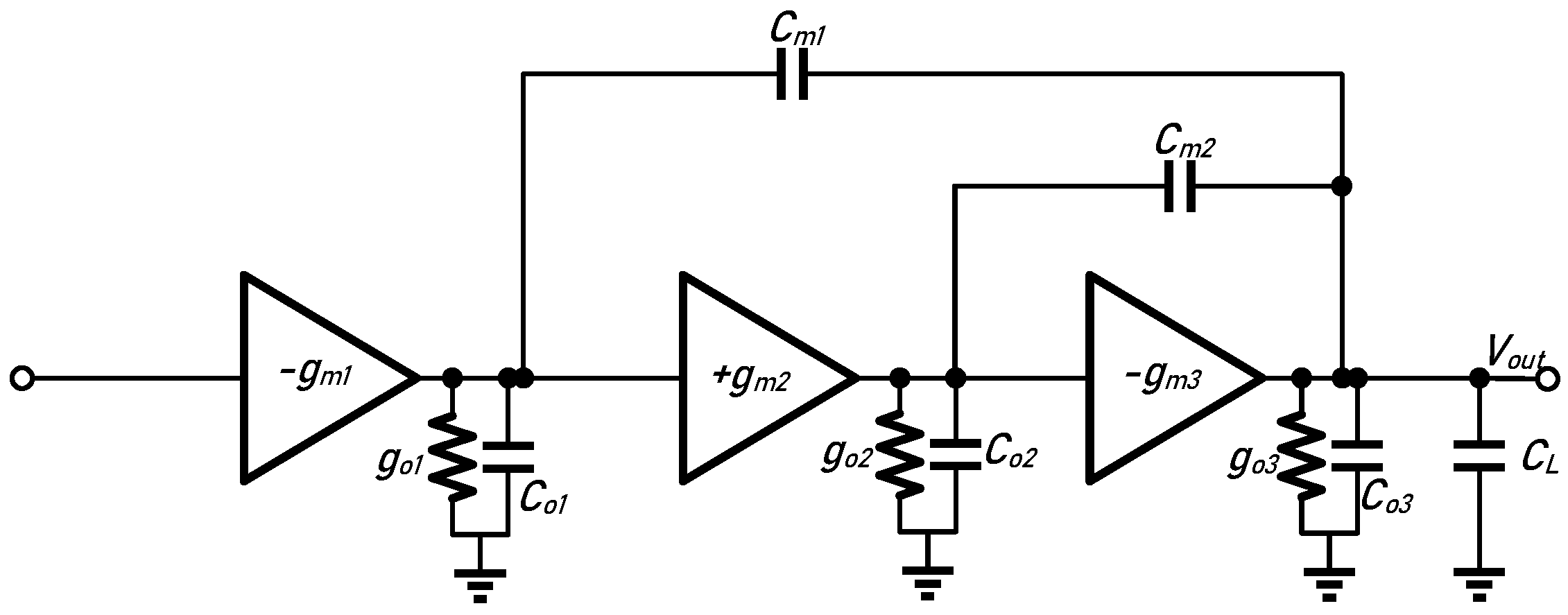
2.1. Review of Frequency Compensation in Three-Stage Amplifier Topologies

Nested Miller compensation (NMC) [6,8] is a popular scheme for high gain amplifier design with good stability with respect to single Miller compensation (SMC) [6]. Figure 1 depicts the NMC configuration for a three-stage amplifier. In principle, NMC can be expanded to an infinite number of stages. However, with more than three stages, the bandwidth is significantly jeopardized.
Referring to Figure 1, gm1-3 are the transconductance of the three-stage amplifier. go1-3 are the output conductance of the amplifier. Co1-3 are the output capacitance of the amplifier, and Cm1 and Cm2 are the two compensation capacitors of the NMC amplifier. Assuming gm3 >> gm1,gm2, the transfer function for a three-stage NMC amplifier is obtained as
A N M C s = A o ( 1 s C m 2 g m 3 s 2 C m 1 ( C m 2 + C o 2 ) g m 2 g m 3 ) ( 1 + s C m 1 g m 2 g m 3 g o 1 g o 2 g o 3 ) 1 + s C m 2 g m 2 + s 2 C L C m 2 g m 2 g m 3
In order to eliminate the peak effect of high-order complex poles, the polynomial is approximated by the Butterworth expression [9]. This is given as follows:
H b u t t e r w o r t h s = A b u t t e r w o r t h s 1 + A b u t t e r w o r t h s = 1 1 + s 2 w 0 + s 2 2 w 0 2 + s 3 1 w 0 3 A b u t t e r w o r t h s = 1 s 2 w 0 1 + s 1 w 0 + s 2 1 2 w 0 2
Relating the Butterworth expression A b u t t e r w o r t h ( s ) and the NMC expression A N M C ( s ) , we obtain
C m 1 = 4 ( g m 1 g m 3 ) C L
C m 2 = 2 ( g m 2 g m 3 ) C L
Then the unity-gain bandwidth (UGB) and phase margin PM become
G B W N M C s = 1 4 g m 3 C L
P M N M C 60 °
Alternatively, Positive Feedback Compensation (PFC) [10] can be used to provide control of the damping ratio of the complex poles, which is achieved through capacitor Cm2. This capacitor, considerably smaller than Cm1, does not cause the significant slew rate (SR) reduction associated with the first stage whilst additionally generating a LHP zero to enhance the PM. The PFC topology is depicted in Figure 2. Of particular note, gm1-3 are the transconductance of the three-stage amplifier. go1-3 are the output conductance of the amplifier. Co1-3 are the output capacitance of the amplifier, and Cm1 and Cm2 are the two compensation capacitors of the PFC amplifier.
The transfer function of the PFC amplifier is given as follows:
H P F C s = g m 1 g m 2 g m 3 R 1 R 2 R L 1 + 2 C m 2 g m 2 s C m 1 C m 2 g m 2 g m 3 s 2 1 + s C m 1 g m 2 g m 3 R 1 R 2 R L 1 + C m 2 2 g m 3 C m 1 g m 2 C L g m 2 g m 3 C m 1 s + C L C m 2 c o 2 g m 2 g m 3 s 2
In order for all poles to be located in the left half plane, each term in the denominator must be greater than 0. This leads to the following design relationship:
2 g m 3 C m 1 g m 2 C L > 0 C m 1 > g m 2 2 g m 3 C L
C m 2 c o 2 > 0 C m 2 > c o 2
Thus, the GBW is obtained as follows:
G B W P F C s = 1 4 g m 3 C L 7 2 g m 2 g m 3 C L C m 2 c o 2
and the PM becomes
P M P F C = 60 ° + tan 1 G B W Z 1 tan 1 G B W Z 2 > 60 °
Another ASMIHF compensation topology [11] is depicted in Figure 3. It employs an active single-Miller capacitor and an inner half-feedforward stage so that it facilitates the stabilization of a three-stage amplifier that is able to drive substantial capacitive loads. This is accomplished through the incorporation of a small feedback compensation capacitor and the utilization of two left LHP zeros. ASMIHF contributes to reduced silicon die area occupation, streamlined design complexity, and enhanced small and large signal performance metrics. In addition, two supplementary and cost-effective feedforward stages, with transconductances gmf1 and gmf2, are employed to enhance stability and achieve a dual-active push–pull operation. gmc1 is the active feedback stage. In conjunction with the gain Av2 of the second stage, it relates ωo and Q in the complex equation. This may affect the circuit stability if not properly designed.
The transfer function of the ASMIHF amplifier is given as follows:
H A S M I H F s = g m 1 R 1 g m 2 R 2 g m 3 R 3 ( 1 + R 1 g m 2 R 2 g m 3 C C s ) · 1 + C C g m c 1 s 1 + g m f 1 C 1 2 g m 2 g m c 1 s 1 + g m f 2 g m c 2 C 2 g m f 1 g m 1 g m 3 s 1 + s ω n · Q + s 2 ω n 2 1 + R 2 C 2 s    
where ω n   = g m 3 g m c 1 A 2 C L C 1 and Q = C C g m 3 A 2 g m c 1 C L C 1 . To obtain a smooth characteristic curve similar to Butterworth’s third-order response, Q is assumed to be 3 2 as an example. This gives g m c 1 = 2 g m 1 , g m c 2 = 3 2 g m 1 g m f 1 C 1 g m c 2 C c , and C C = 3 2 g m 1 C L C 1 g m 3 A 2 , respectively, and the GBW is g m 1 C C . Due to the existence of gmc1 and gmc2, this combination with the load transistor will inevitably form a cascode structure. Therefore, the structure is not suitable for working at a low supply voltage.

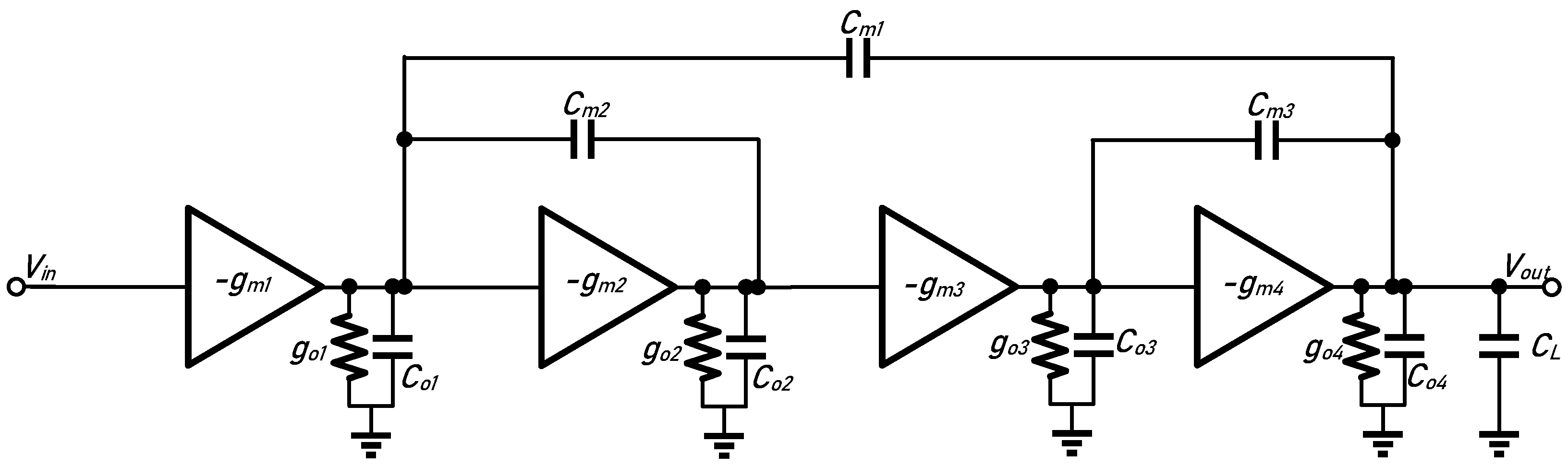
2.2. Review of Frequency Compensation in Four-Stage Amplifier Topologies

Similar to the three-stage op-amp topology, multiple nested Miller compensation [12] is a traditional frequency compensation method in four-stage op-amp design. The multiple nested Miller compensation topology is depicted in Figure 4.
Regarding the topology, gm1-4 are the transconductances of the four-stage amplifier. go1-4 are the output conductances of the amplifier, Co1-4 are the output capacitances of the amplifier, and Cm1, Cm2 and Cm3 are the three compensation capacitors of the multiple NMC amplifier. When dealing with a multi-stage operational amplifier, determining the precise location of nondominant poles can be tedious calculation. Without specific precautions, these poles may interact. Thus, they lead to complex pairs which cause stability issues. The basic rules for this amplifier design are given as follows:
G m i C i 1 2 G m i + 1 C i + 1
G m N G m i ,   i = 1 ,   N 1
where Gmi and Ci are the transconductance and compensation capacitor of the ith stage, respectively. The first stability condition, expressed in (14), requires that each nondominant pole be positioned at a frequency at least two times of the preceding one. The output of the first stage is assumed to contribute the dominant pole, while the outputs of the subsequent n – 1 stages produce the nondominant poles. Nevertheless, the fulfillment of (14) requires considerable constraint on the overall bandwidth of an amplifier when the number of stages increases. In the design of power operational amplifiers, (15) is readily fulfilled. This is attributed to the condition that the transconductance of the final stage must be larger than that of the preceding stages to effectively drive substantial loads.
Alternatively, the hybrid nested Miller compensation (HNMC) structure [13] or the hybrid cascode frequency compensation structure [14] can be used to further improve the achievable bandwidth of a four-stage op-amp. The hybrid nested Miller compensation (HNMC) structure, which is illustrated in Figure 5, has the feedback capacitors across their respective local inverting stages as well as across inverting multi-stages.
As can be seen in Figure 5, two Miller loops involving Cm2 and Cm3 operate on the same nesting level. Cm1 is also a compensation capacitor within the negative feedback loop. gm1-4 are the transconductances of the four-stage amplifier. go1-4 are the output conductances of the amplifier. Co1-4 are the output capacitances of the amplifier. An exemplary frequency compensation condition is achieved as follows:
g m 3 C m 1 C m 1 C m 2 = 1 2 g m 4 C L
where CL is the load capacitor. At this juncture, according to (14), the unity-gain frequency of the op-amp can be obtained as follows:
ω t = g m 1 C m 1 1 4 g m 4 C L
where ω t is the unity-gain frequency of op-amp. Compared with the ω t = 1 2 g m 4 C L of single Miller compensation (SMC), HNMC has only two nested levels, and thus the bandwidth is reduced by half. If multiple nested Miller compensation is used, since it has three nested levels, its bandwidth will be reduced to a quarter of SMC.
Another typology, nested transconductance-capacitance compensation (NGCC) [15], is another way to improve the bandwidth of a four-stage op-amp. The NGCC is depicted in Figure 6.
In general, the i-th module comprises a transconductor gmi, a feed-forward trans-conductor gmfi, an output conductance goi, and a compensation capacitor Coi. The DC voltage gain of the amplifier, as shown in Figure 6, is governed by the combined gain of the n + 1 cascaded stages (gm1, gm2, …, gmn, gmn+1). At high frequencies, when the gain of these stages decreases, the feed-forward transconductance gmf bypasses all stages from (i + 1) to n, effectively extending the overall amplifier bandwidth. When gmi = gmfi, the transfer function of the NGCC amplifier can be obtained as follows:
V o ( s ) V i ( s ) = A 0 ( 1 + A 0 s f 1 ) ( 1 + s f 2 + s 2 f 2 f 3 + + s n 1 i = 2 n f i )
where A 0 = j = 2 n g m j g o j and f i = g m i C m i . The stability conditions for the NGCC-based topology are determined by applying the Routh stability criterion to the unity-gain closed-loop transfer function. This yields the following stability criteria:
f 4 > f 2 1 ( 1 f 1 f 3 )
On the contrary, the stability conditions for multistage NMC amplifiers introduces complexity to the design process. On the other hand, when designing a stable multistage NGCC amplifier, it is more straightforward.
By comparing the bandwidth of a four-stage NGCC amplifier with that of an NMC amplifier and taking frequency normalization with respect to the gain bandwidth (GBW), the following can be obtained:
f 4 G B W = f 4 G B W f 2 + f 3 G B W
where f 4 and GBW are the cut-off frequency and gain-bandwidth product of final stage of NGCC amplifier, respectively, whereas f 2 , f 3 , f 4 and G B W are the cut-off frequencies of the 2, 3, 4 stages and gain-bandwidth product of the final stage of the four-stage NGCC amplifier, respectively. Equation (20) implies that f 4 G B W < f 4 G B W , which means the GBW of NGCC, is greater than that of NMC for the same power ( f 4 = f 4 ). However, all feedforward paths of NGCC are connected to the output of the last stage, which leads to an increase in power consumption.
To achieve higher power efficiency, separate Miller compensation [16], alternative modified topology [17], or active parallel compensation (APC) [18] have been used. Figure 7 shows the separating Miller compensation with feedforward path (SMF) [16].
It is noted that gmi, Roi, and Coi represent the transconductance, output resistance, and capacitance of the nth stage, respectively. The feedforward stage is denoted by gmf. RL and CL indicate the load resistance and capacitance, including the output resistance and capacitance of the final stage. The compensation capacitors are Cm1 and Cm2, while the nulling resistors are Rm1 and Rm2. Cm1 and Rm1 together form the primary Miller compensation signal path for the entire amplifier. A secondary Miller compensation signal path is established by Cm2 and Rm2. The transfer function of the four-Stage SMF amplifier is obtained as follows:
A v s = A D C · 1 + N 1 s + N 2 s 2 + N 3 s 3 ( 1 + s p 0 ) ( 1 + D 1 s + D 2 s 2 + D 3 s 3 )
where
A D C = g m 1 g m 2 g m 3 g m 4 R o 1 R o 2 R o 3 R L
N 1 = R m 1 C m 1 + C m 2 [ R m 2 1 g m 3 + g m f g m 2 g m 4 ]
N 2 = C m 1 C m 2 [ R m 1 R m 2 1 g m 3 + g m f R m 1 1 g m 2 g m 4 ]
N 3 = C o 2 C m 1 C m 2 g m 2 g m 3 g m 4 ( g m f R m 1 1 )
p 0 = 1 C m 1 g m 2 g m 3 g m 4 R o 1 R o 2 R o 3 R L
D 1 = C m 2 [ R m 2 1 g m 3 + g m f g m 2 g m 4 ]
D 2 = C m 2 C L g m 2 g m 4 + g m f C 2 g m 2 g m 3 g m 4 ( C m 2 + C o 3 )
D 3 = C o 2 g m 2 g m 3 g m 4 C m 2 + C o 3 C L + g m f R m 2 C o 3 C m 2 + R m 1 C o 1 C m 2 C L g m 2 g m 4
To enhance push–pull behavior, the nulling resistor should be selected by the following design criteria. They are given as
R m 1 = 1 g m f
R m 2 1 g m 2 , 1 g m 3
Then the GBW and PM can be obtained as follows:
G B W = ω 0 = g m 1 C m 1
P M = 90 t a n 1 [ R m 1 C m 1 ω 0 + ( D 1 D 2 + R m 1 C m 1 ( D 1 2 D 2 ) ) ω 0 3 1 + ( D 1 2 D 2 ) ) ω 0 2 D 1 D 2 R m 1 C m 1 ω 0 4 ]
Separating the nested Miller compensation into two independent Miller compensation networks can improve the power efficiency of the op-amp. However, the compensation scheme may face design challenges in controlling the stability. This stems from the fact that it can only determine the position between the two poles, but not the position between the four poles. As a result, there may be overlap between multiple poles. When multiple poles coincide, there will be a stability problem and the bandwidth will be limited. In the case of ultra-low power design constraints, the extension of higher bandwidth becomes an issue.
In brief, multiple nested Miller compensation is one of the common frequency compensation methods. Because of its many nested levels and excessive capacitance, the bandwidth of the four-stage op-amp will be greatly limited and consume a larger area. According to (14), HNMC designed on the basis of multiple nested Miller compensation has fewer nested levels. By comparing this with SMC, the bandwidth attenuation that it brings is 1 2 of the bandwidth attenuation by multiple nested Miller compensation. Furthermore, the realizable bandwidth of a four-stage HNMC amplifier can be designed the same as that of the three-stage NMC op-amp [15]. NGCC introduces a feedforward circuit and a Miller capacitor to work together for frequency compensation. It can be seen from (19) that NGCC can significantly increase the bandwidth, but this is at the expense of increased power consumption. Based on the review of these frequency compensation schemes, it is important to devise an effective frequency compensation that is suitable for an ultra-low-voltage four-stage amplifier design.

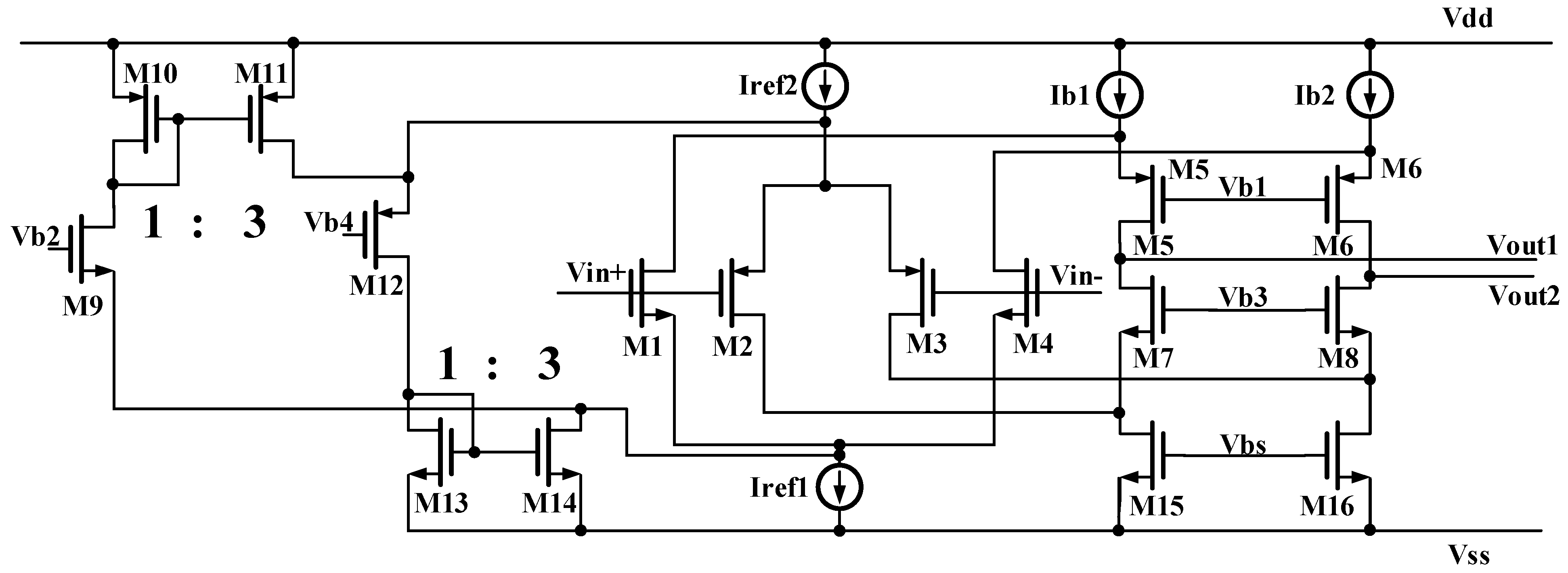
2.3. Review of Low-Voltage Rail-to-Rail Amplifier Circuits

The bulk-driven technique is widely used in low-voltage rail-to-rail circuit design, and the ICMR can offer 0–Vdd range. The two-stage bulk-driven rail-to-rail amplifier, which is realized in differential difference amplifier (DDA) [19] topology, is shown in Figure 8. Transistors M1A-M1B and M3A-M3B are the input differential pairs while the biasing circuit comprises the biasing transistor pairs M2A-M2A, M5A-M5B, M4A-M4B, and M6A-M6B. The cross-coupled transistors M7A and M7B, in association with the diode-connected transistors M8A and M8B, enhance the gain through partial positive feedback by introducing negative transconductance (−gm7). Transistors M9A, M9B, M10A, and M10B form the differential to single-ended conversion for the first-stage gain. Transistors M11 and M12 form the second-stage gain with Miller capacitor CC.
The gain of bulk-driven DDA is
A v _ b u l k d r i v e n = g m i g d s 9 + g d s 10 g m 12 g d s 11 + g d s 12
where
g m i 2 g m b 1,3 g m 9 / g m 8 1 g m 7 g m 8 + g d s 1 + g d s 3 + g d s 7 + g d s 8 g m 8
The GBW is
G B W b u l k d r i v e n = g m i 2 π C C
For bulk-driven circuits, gmbs replaces gm as the transconductance of the circuit. Since gmbs is very small, the gain of the bulk-driven circuit is very small. The same goes for the gain-bandwidth product. As such, the thermal noise performance metric will be worse due to small transconductance in the front-end stage.
The traditional complementary gate-source input stage amplifier [20] is shown in Figure 9. It is regarded as one of the economical circuit techniques by utilizing a 1-to-3 current mirror. The design operates in the saturation region, with a supply voltage of 3.3V. M1-4 are the input differential input pairs which are composed of complementary PMOS and NMOS transistors for rail-to-rail design. M5-6, 7-8 are the cascode transistors and M15-16 are the current source transistors. M10-11, 13-14 are used to implement current mirrors with a 1-to-3 ratio for approximated constant gm design.
The overall transconductance of input stage is defined as
g m i = ( W L ) n µ n C O X I r e f 1 + ( W L ) p µ p C O X I r e f 2
where Iref1,2 are the bias currents of the NMOS pair and PMOS pair, respectively. For complementary circuits without gmi smoothing, the combined gmi of the input stage under either the lower or upper part of common-mode range is half of the overall value. This will be double in value in the middle range. The same goes for unity-gain bandwidth. There are many ways to make the approximated constant gmi. Alternatively, it can be achieved through the level shift approach [21], which relies on the input transistor pairs to operate in the saturation region. Similarly, it also offers less sensitivity on gmi variation against the change of input signal. Unfortunately, when pushing for lower supply, the available signal headroom in conjunction with unavoidable output spikes through the variation of gmi will be reduced. In poor conditions, the rail-to-rail circuit will be jeopardized in operation, and this will be particularly pronounced when the rail-to-rail complementary input pairs are biased in the sub-threshold region for obtaining low power purpose.

3. Proposed Four-Stage Amplifier with Cross-Feedforward Positive Frequency Compensation (CFPFC)

Figure 10 shows the circuit of the proposed four-stage amplifier in TSMC 40 nm process technology. The amplifier consists of a bias circuit, a bulk-drain transistor input stage, an attenuation stage, and a high-gain stage. The bias circuit consists of a supply-independent topology and a start-up network (MB1-6, CB1-2). For the input stage, it consists of the complementary topology which is embedded with the bulk-drain differential pairs (Mp1-2, Mn1-2) and the respective load transistors (M3-6). This is then followed by the attenuation stage (Mna1-Mna4, M7, 8) in a source–follower-like topology, comprising two native transistors and one low-threshold transistor in each output of the first stage.
As mentioned before, the rail-to-rail input circuits, under a low supply voltage and a subthreshold operation region, can influence subsequent amplification stages through large variations in the first stage’s output spike under high fluctuations of gmi. Moreover, under limited supply, the IMCR becomes ineffective in the gate-source biased differential pairs despite the gmi obtained from a gate-source biased transistor being relatively higher than that of a bulk-driven transistor.
Regarding the bulk-driven input stage, this has high ICMR capability through the use of gmb as the main transconductance. However, its gain and driving capabilities are low. For this reason, the bulk-drain-driven [22] differential pairs are introduced to obtain the design tradeoff between the gate-source or bulk-driven techniques. This can offer an improved IMCR with respect to that of the gate-source driven technique, whilst the transconductance is not reduced significantly due to weak degeneration arising from bulk-drain transistor topology. As a result of this weak degeneration, the amplifier’s parameters such as noise, gain, and bandwidth are still higher than that of bulk-driven circuits. Furthermore, in comparison with bulk-drain-driven circuits, the temperature effect of bulk-driven is less obvious [22]. As a result, the bulk-drain-driven circuit can provide a compromising design solution among the transconductance and signal swing in low-voltage design.
The use of native transistors (with negative threshold voltage) ensures low-voltage operation. As such, the use of diode-based transistors permits attenuation of any spike [22] that appears through the transition change of transconductance from the complementary differential pairs. This reduced spike will not overdrive the subsequent stage, thus does not jeopardize the amplification in the next circuit stage. In this way, it is economical to remove the conventional transconductance smoothing circuits [23,24,25]. This is particularly useful because it offers simplicity whilst reducing the power consumption and complexity as well as avoiding a higher supply in conventional methods.
After the low-voltage attenuator, it is the high-gain stage that drives the 50 pF capacitive load. This gain stage (M9-20) contains two non-inverting amplifiers, one push–pull stage, three feed-forward paths, and the capacitors (Cm1-2) dedicated to the positive frequency compensation.
The cross-feedforward paths, with which to bypass the respective stage, enhance the bandwidth as well as the stability of the PFC amplifier. Furthermore, introducing a positive feedback loop effectively governs the damping ratio of the complex poles. This can be achieved by fulfilling the design equations for the compensation capacitors in subsequent transfer function analysis. By properly sizing the compensation capacitors, the usual RHP poles can be moved to LHP for stability. Furthermore, both FF and PFC yield LHP zeros to ensure stability in multi-stage amplifier design.
Figure 11 depicts the block diagram of the proposed four-stage amplifier. Assuming that the parasitic capacitances in each stage are neglectable, the open-loop transfer function of the amplifier is obtained as follows:
A C F P F C s = A 1 + B s + C s 2 + D s 3 1 + E s + F s 2 + G s 3 1 + H s 1 + I s
where
A = R 1 R 2 R 4 R 5 R 6 g m 1 g m 4 g m 5 g m 6 g m b u f f e r 1 B = C m 2 g m f 2 g m 4 g m 5 C = C m 2 C 5 g m 4 + C m 1 g m 4 + C m 1 g m f 2 g m 4 g m 5 g m 6 D = C 1 C m 1 C m 2 R 1 R 4 R 5 g m f 1 E = C L R 6 C m 1 R 4 R 5 g m 5 + C m 2 R 4 R 5 R 6 g m 5 g m 6 F = R 4 R 6 C L C m 2 C L C m 1 R 5 g m 5 + C m 1 C m 2 R 5 g m 5 + C m 1 C m 2 R 5 g m 6 + C m 1 C m 2 R 5 g m f 3 G = C L R 4 R 5 R 6 C 5 C m 2 + C m 1 C m 2 H = C 1 C 1 I = C 2 R 2
For positive feedback compensation, the most important thing is to consider the instability which comes from two aspects:
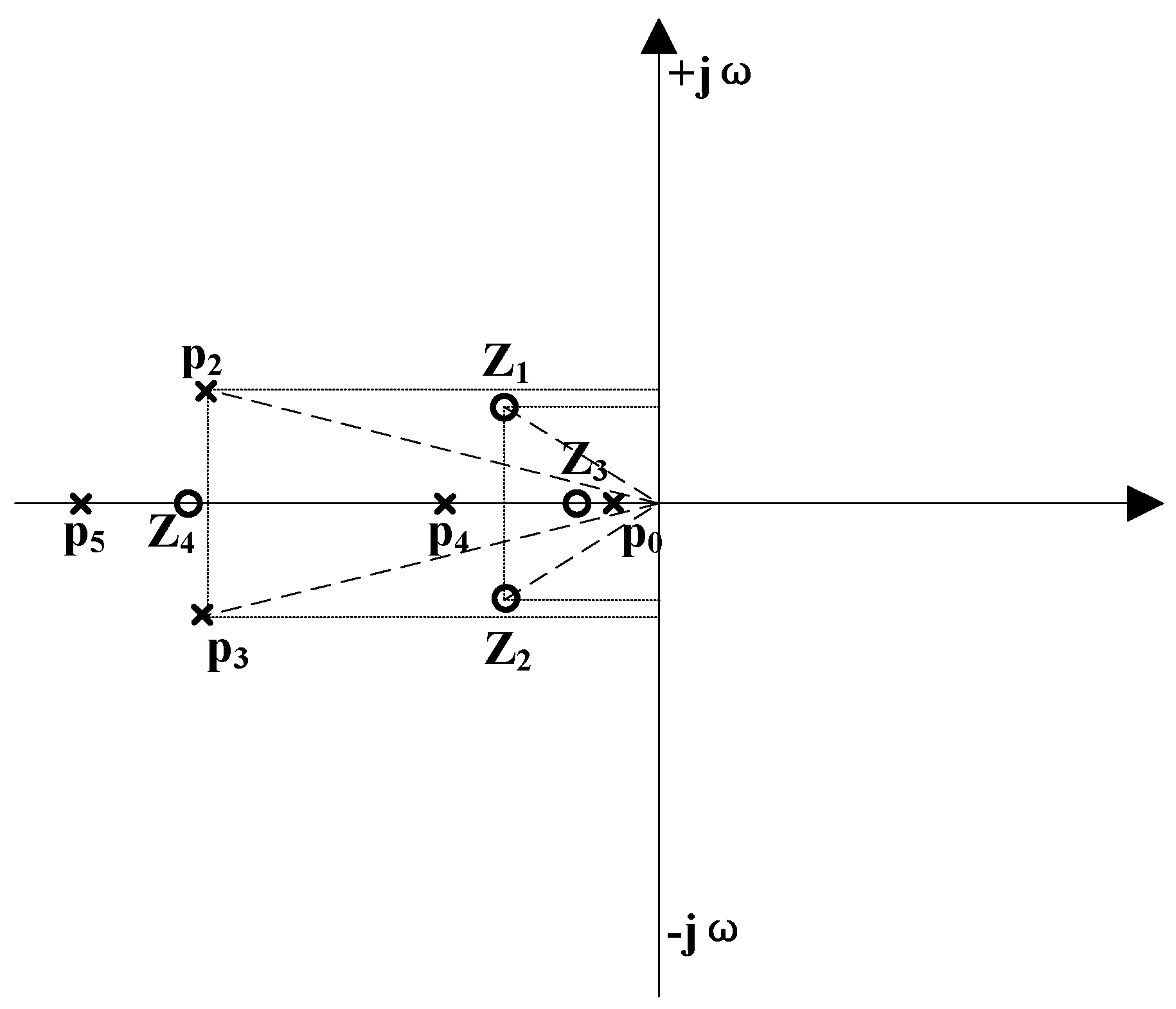
  • There may be a RHP pole that causes oscillation;
  • The peak introduced by the existence of high-order complex polynomial.
In order to tackle the first issue, all the poles must be located in LHP. This requires each coefficient of the denominator to be greater than 0. Thus, we have
E > 0 C m 1 < C L R 6 + C m 2 R 4 R 5 R 6 g m 5 g m 6 R 4 R 5 g m 5 C m 2 R 6 g m 6
F > 0 C m 2 > C L C m 1 R 5 g m 5 C L + C m 1 R 5 g m 5 + g m 6 + g m f 3 C m 1 R 5 g m 5
This yields the need for a larger Cm2 and a smaller Cm1. At this juncture, due to the introduction of the feedforward path, the compensation capacitor Cm2 in the CFPFC amplifier can be made smaller than that in the PFC amplifier without a feedforward design. As a result, this achieves increased bandwidth while keeping a small area arising from the capacitors. Regarding the peak effect caused by the high-order complex pole equation, it is necessary to choose the damping ratio by controlling the ratio between Cm1 and Cm2 so as to permit the loop gain curve to be as smooth as possible. According to Butterworth Equations (2) and (3), it is necessary to arrange the higher-order complex pole equation into a similar form. Assuming C L C m 2 C m 1 , the transfer function becomes
A C F P F C s = A 1 + E s 1 + F E s + G E s 2 1 + H s 1 + I s
By replacing E, F, G with ω 0 and ω n , we get
A C F P F C s = A 2 ω 0 s 1 + 1 ω 0 s + 1 2 ω 0 2 s 2 1 + H s 1 + I s
A C F P F C s = A 2 2 ω n s 1 + 2 ζ 1 ω n s + 1 ω n 2 s 2 1 + H s 1 + I s
where ω 0 is the dominant pole, ω n is the non-damped frequency. Therefore, the secondary poles are
p 2,3 = ω n = 2 ω 0
Then, with ζ = 2 2 , we can obtain the following relationship.
2 ω 0 = E
1 ω 0 = F E
1 2 ω 0 2 = G E
By solving the above equations, we have obtained the design equations for the compensation capacitors and the dominant pole. They are given as follows:
C m 1 = 2 R 5 2 g m 5 g m 6 C L
C m 2 = 2 R 4 R 5 2 R 6 g m 5 2 g m 6 2 C L
ω 0 = R 5 g m 5 g m 6 C L
As a result, within the bandwidth, there is no peak effect caused by high-order complex poles. Since gm2 is derived from the attenuation buffer output (source output), its resistance R2 is very small and so is the time constant R2C2. From (41), p4 is (1/I) and p5 is (1/H). These are high-frequency poles when compared with other poles. At this juncture, considering the main pole ω0 and the secondary poles ω2,3, the expression can be obtained as follows:
G B W C F P F C = ω 0 2
P M C F P F C = 180 ° tan 1 G B W p 3 d B tan 1 2 ζ G B W p 2.3 1 G B W p 2.3 2 60 °
Incorporating the effect of higher frequency zero, z1, the PM becomes
P M C F P F C = 60 ° + tan 1 G B W z 1 > 60 °
Figure 12 shows the pole-zero location of CFPFC op-amp. p0 is the dominant pol, p2, p3 are complex poles, and p4, p5 are the high-frequency poles produced by H and I in Equation (41). Of particular note, z1, z2, z3 are the high-frequency LHP zeros caused by the feedforward paths and PFC. Through the stated design criteria for the compensation capacitors, the complex poles p2, p3 are now moved to the LHP. The dimensions of each device are listed in Table 1.

4. Results and Discussion

The four-stage op-amp is designed and implemented using TSMC 40 nm CMOS process technology. The circuit operates at 0.5 V supply and drives the capacitive load of 50 pF.
Figure 13 shows the simulated DC gain, gain bandwidth (GBW), phase margin (PM), and gain margin (GM) of the proposed amplifier at different corners. At the tt corner, the corresponding values are 84.588 dB, 161 kHz, 96 degrees, and 5.7 dB. At the ss corner, the respective values are 88.2 dB, 65.9 kHz, 76.11 degrees, and 8.23 dB. At the ff corner, the respective values are 75.37 dB, 247.9 kHz, 101.66 degrees, and 11.94 dB. It can be observed that the amplifier is stable at all corners and maintains high gain despite some deviations in gain-bandwidth across the corners.
Figure 14 depicts the power-supply gain of the proposed amplifier. These are obtained as −56.02 dB at tt, −61.35 dB at ss, and −43.37 dB at ff, respectively. Regarding the power supply rejection ratio (PSRR), the obtained values are 56.02 dB at tt, 61.35 dB at ss, and 43.37 dB at ff, respectively. Figure 15 depicts the common-mode gain of the proposed amplifier. These are −57.11 dB at tt, −66.76 dB at ss, and −42.61 dB at ff, respectively. These yield the common-mode rejection ratio (CMRR) of 57.11 dB at tt, 66.76 dB at ss, and 42.61 dB at ff, respectively. Due to the high differential-mode gain at low frequency, the obtained PSRR and CMRR values are high.
Figure 16 illustrates 200 runs of Monte Carlo simulations pertaining to offset voltage. The mean offset voltage is 0.391 mV, which is less than 1 mV. This suggests that the op-amp exhibits low offset in the context of process variation.
Figure 17 shows the plot of output swing (y-axis) against the input range (x-axis). This is based on the unity-gain configuration with different input stage designs with/without a low-voltage attenuator in the amplifier at tt condition. The input voltage Vg of all input transistors is kept at 250 mV while the supply voltage Vdd is kept at 500 mV and the drain current ID is kept at 150 nA. The simulation results are shown in Figure 17. The first curve refers to the proposed bulk-drain-driven input topology with the embedded attenuator, and the obtained ICMR is 194 mV (116 mV to 310 mV). The second curve refers to the bulk-drain-driven input topology but without an attenuator, and the obtained ICMR is 105 mV (227 mV to 332 mV). The third curve denotes the gate-source driven input topology together with an attenuator, and the obtained ICMR is 147 mV (126 mV to 273 mV). The fourth curve denotes the gate-source driven input topology without an attenuator, and the obtained ICMR is 70 mV (224 mV to 294 mV). It can be confirmed that the proposed bulk-drain-driven input topology with an attenuator can effectively improve ICMR with respect to that gate-source driven topology with and without an attenuator.
Figure 18 shows the plot of output swing (y-axis) of a proposed amplifier against the input range (x-axis). This is based on the unity-gain configuration driving a 50 pF load at different corners. As observed, the input range is from 116.3 mV to 310 mV at the tt condition, 90.0 mV to 370 mV at the ss condition, and from 160 mV to 310 mV at the ff condition. From the results, at supply of 0.5 V, the bulk-drain-driven input topology in conjunction with the low-voltage attenuator in amplifier’s architectural design permits a swing of up to 40% of Vdd.
The transient responses of the proposed amplifier are shown in Figure 19. The period of the input square wave is 5 ms, and the rise time and fall time are 1 µs, respectively. It can be seen that the obtained slew rates are 0.064 V/μs and 0.017 V/μs at tt, 0.005 V/μs and 0.0025 V/μs at ss, and 0.005 V/μs and 0.006 V/μs at ff, respectively. In addition, the settling time is 72.49 μs at tt, 116.58 μs at ss, and 58.35 μs at ff, respectively. Due to the low-power design, the SR is limited but it can be improved through the use of a SR enhancement circuit or an increase in power consumption.
The input-referred noise simulation results are shown in Figure 20. At 1 kHz, the input-referred noise can be obtained as 213.63 nV/ H z at tt, 343.96 nV/ H z at ss, and 214.91 nV/ H z at ff, respectively. Due to relatively higher gmi being obtained from the rail-to-rail bulk-drain-driven topology, the noise performance metrics are better when compared to the bulk-driven input stage design. This also proves that the degeneration effect from the bulk-drain transistor is not significant. Therefore, it is not of concern.
The simulation results pertaining to the variation of input stage transconductance, gmi, against the input voltage with and without a low-voltage attenuator are shown in Figure 21. It can be observed that due to the complementary circuit, gmi will exhibit an obvious spike at the first output stage. Nevertheless, this spike is significantly suppressed after passing through the attenuator. This has demonstrated the effectiveness of using an attenuator to tackle the gmi variation. Although the attenuator will attenuate the signal gain, the overall gain will be compensated by the subsequent high-gain stage.
Figure 22, Figure 23, Figure 24, Figure 25, Figure 26, Figure 27 and Figure 28 illustrate 200 runs of Monte Carlo simulations pertaining to DC gain, GBW, PM, GM, CMRR, PSRR, and noise with estimated layout parasitics, respectively. According to Figure 22 and Figure 23, the mean DC gain and GBW are 84.01 dB and 153.8 kHz, respectively, which are close to the simulation results without considering the parasitic capacitances. Regarding Figure 24 and Figure 25, the mean PM and GM are 79.39 deg and 4.7 dB, respectively. Despite some reduction in PM and GM, these are still acceptable after taking into account parasitic effects, as PM is still maintained at a high rate. As seen in Figure 26 and Figure 27, the mean CMRR and PSRR are 49.3 dB and 49.1 dB, respectively. There is no significant difference when taking the parasitic effect into account. The mean noise is obtained as 205.47 n V / H z , which shows that the op-amp’s noise is still low when including the parasitic effect according to Figure 28. Figure 29 shows that the mean power consumption is 0.95 μW. These suggest that the op-amp exhibits good performance in the context of process variation and parasitic effects.
The total current of the entire circuit is 1.73 µA, and the power consumption of the amplifier is only 0.865 μW at 0.5 V. In order compare the performance of amplifiers, different Figure-of-Merits are introduced. FoMss [23] and IFoMss [16] are used to quantify the performance of amplifiers under small-signal conditions. They are defined as follows:
F o M s s = U G B × C L P w
I F o M s s = U G B × C L I d
where UGB is the unity-gain bandwidth, CL is the load capacitor, Pw is the power consumption, Id is the total current consumption, PM is the phase margin, and Ts is the settling time. Higher values of FoMss and IFoMss indicate better performance metrics. Furthermore, FoMls [23] and IFoMls [16] are used to quantify the large-signal performance of amplifier. They are defined as follows:
F o M l s = S R × C L P w
I F o M l s = S R × C L I d
where SR is slew rate. Similarly, higher values of FoMls, and IFoMls indicate better performance metrics. Finally, in order to compare the effectiveness of amplifiers among the tradeoff performance metrics which involve multiple parameters such as noise, power consumption, and unity-gain bandwidth, a FoMnpb (FoMnoise-power per bandwidth) is used for the evaluation. It is given as follows:
FoMnpb =Pw × Input-referred Noise@1 kHz/UGB
The lower the value of FoMnpb, the better the tradeoff performance.
The simulation results of the proposed amplifier show that FoMss and FoMls are 9.31 MHz∙pF/μW and 2.34 (V∙pF)/(μs∙μW), respectively, while FoMnpb is 1.15 × 10⁻⁶ (( µ V / H z )·µW/Hz). IFoMss and IFoMls are 4.65 (MHz∙pF/μA) and 1.17 ((V∙pF)/(μs∙uA)), respectively. The simulation parameters of each process corner at 27 °C are shown in Table 2.
In order to evaluate the PVT variation as well as the impact of layout parasitics on the circuit performance, Table 3 shows the comparative simulation results taking into account the process corners, supply voltage, and temperature together with the simulation results which are based on the estimated layout parasitics under a typical case. Table 4 shows the comparison between the performance results of a typical case and the mean values of the performance metrics obtained from 200 runs of Monte Carlo simulations with estimated layout parasitics. It can be seen that the proposed amplifier can work under the two worst PVT conditions. On top of that, the estimated layout parasitics which are added in the circuit had no significant impact on circuit performance. This is mainly because the circuit is designed at a low-frequency operation.
Compared with other capacitive load-driven designs which have power supply voltages of 0.5 V or below in Table 5 and Table 6, FoMss and IFoMss have comparable improvement. However, due to power limitations, FoMls and IFoMls become smaller, but they can be improved through adding an SR boosting circuit or the increase of power consumption if the design is permitted. Finally, this also reveals that the FoMnpb of the proposed work is obviously better than other reported designs. This has validated that the proposed work has good tradeoff efficiency.
We compared the four-stage amplifier designs with different types of load in Table 7. Despite CFPFC having a relatively lower value of FoMss and FoMls with respect to that of [16,18], it is regarded as an acceptable value because its power consumption is merely 1/1617 in [16] and 1/180 in [18]. Furthermore, the existence of low-frequency parasitic poles under extreme low-power specifications will lead to design challenges in the frequency compensation.
In order to compare the Cadence Spectre simulation results, an analytical MATLAB model on the basis of Equation (41) is developed. This aims at achieving an in-depth understanding of parameters that influence the transfer function. In Figure 30, the blue dotted line is the tt corner simulation data derived from Cadence Spectre, whereas the red solid line is the transmission function illustrated by MATLAB. The left side is the gain and the right side is the phase. It can be seen that the errors among the curves are small (less than 10%). Compared with the results of Spectre, the error is 0.1% (84.05 dB/84.588 dB) in DC gain, 1.9% (5.185 Hz/5.284 Hz) in dominant pole and 8.70% (175 kHz/161 kHz) in UGB. This validates the analytical Equation (41) from theory.
Compared with other designs with supply voltage ≤ 0.5 V, the proposed design can achieve higher gain and higher bandwidth. Both PSRR and CMRR can also reach a moderate level with respect to that of other designs. Even with mismatches under Monte-Carlo simulation runs, the offset voltages are reasonable. In addition, through the use of bulk-drain-driven input topology in association with the embedded low-voltage attenuator in the amplifier’s architectural design, the ICMR of the proposed amplifier is larger than the gate-source driven topology. In addition, the multi-parameter FoM performance metrics pertaining to noise, power, and bandwidth are introduced. Compared with other four-stage amplifier designs of different compensation typologies, the reduction of FoMss and FoMls is the inevitable tradeoff due to the ultra-low and constrained power design. Finally, the proposed circuit operates stably under PVT variations and is insensitive to parasitics due to the low operating frequencies.

5. Conclusions

This paper presents a new 0.5 V four-stage amplifier design that operates at low voltage and low power consumption. Using the bulk-drain-driven input stage allows the op-amp to obtain moderately good gmi while achieving an improved input common-mode range with respect to the complementary rail-to-rail input circuit. This maintains the benefits of low noise and good bandwidth even under low bias current when compared with that of a bulk-driven input stage design. More importantly, the use of a low-voltage attenuator in its architectural design reduces the impact of the output spikes caused by fluctuation of gmi against input signal, thus sustaining the operation of the circuit at very low supply voltages. Furthermore, through the use of cross-feedforward positive feedback compensation, the circuit is verified to have good stability even when the amplifier is realized in a four-stage design. As a result, when the amplifier is compared with prior works, it exhibits good small-signal power-bandwidth FoMss and good multi-parameter FoMnpb with reference to those of bulk-driven designs. This has demonstrated the usefulness of amplifier architecture and the frequency compensation technique. The amplifier is useful for low-voltage analog signal processing applications.

Author Contributions

Conceptualization: F.G. and P.K.C.; Validation: F.G. and P.K.C.; Writing: F.G.; Review and Editing: P.K.C. All authors have read and agreed to the published version of the manuscript.

Funding

This research received no external funding.

Institutional Review Board Statement

Not applicable.

Informed Consent Statement

Not applicable.

Data Availability Statement

Data are contained within the article.

Conflicts of Interest

The authors declare no conflict of interest.

References

  1. Xia, F.; Yang, L.T.; Wang, L.; Vinel, A. Internet of Things. Int. J. Commun. Syst. 2012, 25, 1101–1102. [Google Scholar] [CrossRef]
  2. Weber, R.H.; Weber, R. Internet of Things: Legal Perspectives; Springer: Berlin/Heidelberg, Germany, 2010. [Google Scholar] [CrossRef]
  3. Rose, K.; Eldridge, S.; Chapin, L. The Internet of Things: An Overview. Internet Soc. (ISOC) 2015, 80, 1–50. [Google Scholar]
  4. Qiu, J.; Jiang, H.; Ji, H.; Zhu, K. Comparison between four piezoelectric energy harvesting circuits. Front. Mech. Eng. China 2009, 4, 153–159. [Google Scholar] [CrossRef]
  5. Woo, K.-C.; Yang, B.-D. A 0.25-V Rail-to-Rail Three-Stage OTA with an Enhanced DC Gain. IEEE Trans. Circuits Syst. II 2020, 67, 1179–1183. [Google Scholar] [CrossRef]
  6. Leung, K.N.; Mok, P. Analysis of multistage amplifier-frequency compensation. IEEE Trans. Circuits Syst. I 2001, 48, 1041–1056. [Google Scholar] [CrossRef]
  7. Chong, S.S.; Chan, P.K. Cross Feedforward Cascode Compensation for Low-Power Three-Stage Amplifier with Large Capacitive Load. IEEE J. Solid-State Circuits 2012, 47, 2227–2234. [Google Scholar] [CrossRef]
  8. Leung, K.N.; Mok, P. Nested Miller compensation in low-power CMOS design. IEEE Trans. Circuits Syst. II 2001, 48, 388–394. [Google Scholar] [CrossRef]
  9. Leung, K.N.; Mok, P.; Ki, W.-H.; Sin, J. Three-stage large capacitive load amplifier with damping-factor-control frequency compensation. IEEE J. Solid-State Circuits 2000, 35, 221–230. [Google Scholar] [CrossRef]
  10. Ramos, J.; Steyaert, M.S.J. Positive Feedback Frequency Compensation for Low-Voltage Low-Power Three-Stage Amplifier. IEEE Trans. Circuits Syst. I 2004, 51, 1967–1974. [Google Scholar] [CrossRef]
  11. Marano, D.; Grasso, A.D.; Palumbo, G.; Pennisi, S. Optimized Active Single-Miller Capacitor Compensation with Inner Half-Feedforward Stage for Very High-Load Three-Stage OTAs. IEEE Trans. Circuits Syst. I 2016, 63, 1349–1359. [Google Scholar] [CrossRef]
  12. Pernici, S.; Nicollini, G.; Castello, R. A CMOS low-distortion fully differential power amplifier with double nested Miller compensation. IEEE J. Solid-State Circuits 1993, 28, 758–763. [Google Scholar] [CrossRef]
  13. Eschauzier, R.; Hogervorst, R.; Huijsing, J. A programmable 1.5 V CMOS class-AB operational amplifier with hybrid nested Miller compensation for 120 dB gain and 6 MHz UGF. IEEE J. Solid-State Circuits 1994, 29, 1497–1504. [Google Scholar] [CrossRef]
  14. Aminzadeh, H.; Ballo, A.; Grasso, A.; Valinezhad, M.; Jamali, M. Hybrid Cascode Frequency Compensation for Four-Stage OTAs Driving a Wide Range of CL. IEEE Trans. Very Large Scale Integr. (VLSI) Syst. 2023, 31, 1665–1674. [Google Scholar] [CrossRef]
  15. You, F.; Embabi, S.H.K.; Sanchez-Sinencio, E. A multistage amplifier topology with nested Gm-C compensation for low-voltage application. In Proceedings of the 1997 IEEE International Solids-State Circuits Conference. Digest of Technical Papers, San Francisco, CA, USA, 8 February 1997; 40, pp. 348–349. [Google Scholar] [CrossRef]
  16. Yan, W.; Kolm, R.; Zimmermann, H. Efficient four-stage frequency compensation for low-voltage amplifiers. In Proceedings of the 2008 IEEE International Symposium on Circuits and Systems, Seattle, WA, USA, 18–21 May 2008; pp. 2278–2281. [Google Scholar] [CrossRef]
  17. Grasso, A.D.; Palumbo, G.; Pennisi, S. High-Performance Four-Stage CMOS OTA Suitable for Large Capacitive Loads. IEEE Trans. Circuits Syst. I 2015, 62, 2476–2484. [Google Scholar] [CrossRef]
  18. Fordjour, S.A.; Riad, J.; Sánchez-Sinencio, E. A 175.2-mW 4-Stage OTA with Wide Load Range (400 pF–12 nF) Using Active Parallel Compensation. IEEE Trans. Very Large Scale Integr. (VLSI) Syst. 2020, 28, 1621–1629. [Google Scholar] [CrossRef]
  19. Khateb, F.; Kulej, T. Design and Implementation of a 0.3-V Differential Difference Amplifier. IEEE Trans. Circuits Syst. I 2018, 66, 513–523. [Google Scholar] [CrossRef]
  20. Hogervorst, R.; Wiegerink, R.J.; De Jong, P.A.L.; Fonderie, J.; Wassenaar, R.F.; Huijsing, J.H. CMOS low-voltage operational amplifiers with constant-gm rail-to-rail input stage. Analog Integr. Circuits Signal Process. 1994, 5, 135–146. [Google Scholar] [CrossRef]
  21. Ibáñez, M.J.; Roldán, J.B.; Roldán, A.M.; Yáñez, R. A comprehensive characterization of the threshold voltage extraction in MOSFETs transistors based on smoothing splines. Math. Comput. Simul. 2014, 102, 1–10. [Google Scholar] [CrossRef]
  22. Lee, J.; Chan, P.K. A 0.5 V Inverter-Based Analog Output-Capacitorless Low-Dropout Regulator with Bulk-Driven Transient-Enhancing Paths. In Proceedings of the 2022 11th International Conference on Communications, Circuits and Systems (ICCCAS), Singapore, 13–15 May 2022; pp. 44–49. [Google Scholar] [CrossRef]
  23. Dehghani, R.; Danesh, A.R. A high-constant gm rail-to-rail operational amplifier using bump-smoothing technique with stabilized output stage. Analog Integr. Circuits Signal Process. 2020, 103, 273–281. [Google Scholar] [CrossRef]
  24. Zazerin, A.; Orlov, A.; Bogdan, O. Modified operational transconductance amplifier macromodel application in piezoelectric active filter design. In Proceedings of the 2014 IEEE 34th International Scientific Conference on Electronics and Nanotechnology (ELNANO), Kyiv, Ukraine, 15–18 April 2014; pp. 373–377. [Google Scholar] [CrossRef]
  25. Kulej, T.; Khateb, F.; Arbet, D.; Stopjakova, V. A 0.3-V High Linear Rail-to-Rail Bulk-Driven OTA in 0.13 μm CMOS. IEEE Trans. Circuits Syst. II 2022, 69, 2046–2050. [Google Scholar] [CrossRef]
  26. Gangineni, M.; Ramirez-Angulo, J.; Vázquez-Leal, H.; Huerta-Chua, J.; Lopez-Martin, A.J.; Carvajal, R.G. ±0.3V Bulk-Driven Fully Differential Buffer with High Figures of Merit. J. Low Power Electron. Appl. 2022, 12, 35. [Google Scholar] [CrossRef]
  27. Khateb, F.; Kulej, T.; Kumngern, M.; Arbet, D.; Jaikla, W. A 0.5-V 95-dB rail-to-rail DDA for biosignal processing. AEU—Int. J. Electron. Commun. 2022, 145, 154098. [Google Scholar] [CrossRef]
  28. Khateb, F.; Kulej, T.; Akbari, M.; Tang, K.T. A 0.5-V multiple-input bulk-driven OTA in 0.18-μm CMOS. IEEE Transactions on Very Large Scale Integr. (VLSI) Syst. 2022, 30, 1739–1747. [Google Scholar] [CrossRef]
  29. Faraji Baghtash, H. A 0.4 V, tail-less, fully differential transconductance amplifier: An all inverter-based structure. Analog Integr. Circuits Signal Process. 2020, 104, 1–15. [Google Scholar] [CrossRef]
  30. Kulej, T.; Khateb, F. A Compact 0.3-V Class AB Bulk-Driven OTA. IEEE Trans. Very Large Scale Integr. (VLSI) Syst. 2020, 28, 224–232. [Google Scholar] [CrossRef]
  31. Kulej, T.; Khateb, F. A 0.3-V 98-dB Rail-to-Rail OTA in 0.18 μm CMOS. IEEE Access 2020, 8, 27459–27467. [Google Scholar] [CrossRef]
Figure 1. Topology of a three-stage NMC amplifier.
Chips 03 00001 g001
Figure 2. Topology of a three-stage PFC amplifier.
Chips 03 00001 g002
Figure 3. Topology of a three-stage ASMIHF amplifier.
Chips 03 00001 g003
Figure 4. Topology of a four-stage multiple nested Miller compensation amplifier.
Chips 03 00001 g004
Figure 5. Topology of a four-stage HNMC amplifier.
Chips 03 00001 g005
Figure 6. Topology of a four-stage NGCC amplifier.
Chips 03 00001 g006
Figure 7. Topology of a four-stage SMF amplifier.
Chips 03 00001 g007
Figure 8. Bulk-driven rail-to-rail DDA circuit.
Chips 03 00001 g008
Figure 9. Gate-source driven rail-to-rail amplifier circuit with 3-to-1 ratio current mirror.
Chips 03 00001 g009
Figure 10. Circuit of the proposed amplifier.
Chips 03 00001 g010
Figure 11. Block diagram of proposed amplifier.
Chips 03 00001 g011
Figure 12. Pole-zero location in CFPFC op-amp.
Chips 03 00001 g012
Figure 13. Open-loop gain under 50 pF load. (a) Open-loop gain and phase at tt corner. (b) Open-loop gain and phase at ss corner. (c) Open-loop gain and phase at ff corner.
Chips 03 00001 g013
Figure 14. Power-supply gain under 50 pF load.
Chips 03 00001 g014
Figure 15. Common-mode gain under 50 pF load.
Chips 03 00001 g015
Figure 16. Histogram of offset voltage under 200 runs of Monte Carlo simulations at 50 pF load.
Chips 03 00001 g016
Figure 17. Common mode range of input and output with different input topology designs with/without low-voltage attenuator.
Chips 03 00001 g017
Figure 18. Common mode range of input and output under 50 pF load.
Chips 03 00001 g018
Figure 19. Transient response and slew rate of proposed amplifier.
Chips 03 00001 g019
Figure 20. Input noise under 50 pF load.
Chips 03 00001 g020
Figure 21. Simulation of gmi against different input common-mode voltages.
Chips 03 00001 g021
Figure 22. Histogram of DC gain under 200 runs of Monte Carlo simulations with estimated parasitics.
Chips 03 00001 g022
Figure 23. Histogram of GBW under 200 runs of Monte Carlo simulations with estimated parasitics.
Chips 03 00001 g023
Figure 24. Histogram of PM under 200 runs of Monte Carlo simulations with estimated parasitics.
Chips 03 00001 g024
Figure 25. Histogram of GM under 200 runs of Monte Carlo simulations with estimated parasitics.
Chips 03 00001 g025
Figure 26. Histogram of CMRR under 200 runs of Monte Carlo simulations with estimated parasitics.
Chips 03 00001 g026
Figure 27. Histogram of PSRR under 200 runs of Monte Carlo simulations with estimated parasitics.
Chips 03 00001 g027
Figure 28. Histogram of noise under 200 runs of Monte Carlo simulations with estimated parasitics.
Chips 03 00001 g028
Figure 29. Histogram of Pw under 200 runs of Monte Carlo simulations with estimated parasitics.
Chips 03 00001 g029
Figure 30. Comparison of open-loop results between spectra simulation and MATLAB models at 50pF capacitive load.
Chips 03 00001 g030
Table 1. Device size of proposed amplifier.
TransistorSize (Type)TransistorSize (Type)
MB120/1 (1.1 V low VTH)MB220/1 (1.1 V low VTH)
MB31.5/1 (1.1 V low VTH)MB412/1 (1.1 V low VTH)
MB550/1 (1.1 V standard)MB61/1 (1.1 V standard)
CB110 pFCB210 pF
RB4.2 MΩ
MP1200/1 (1.1 V low VTH)MP2200/1 (1.1 V low VTH)
MN140/1 (1.1 V low VTH)MN240/1 (1.1 V low VTH)
M316/1 (1.1 V low VTH)M416/1 (1.1 V low VTH)
M51/7 (1.1 V low VTH)M61/7 (1.1 V low VTH)
Mna10.5/22 (2.5 V native)Mna2 1/10 (1.1 V native)
Mna30.5/22 (2.5 V native)Mna41/10 (1.1 V native)
M750/1 (1.1 V low VTH)M850/1 (1.1 V low VTH)
M970/1 (1.1 V low VTH)M1072/1 (1.1 V low VTH)
M114/1 (1.1 V low VTH)M124/1 (1.1 V low VTH)
M1313/1 (1.1 V low VTH)M1416/1 (1.1 V low VTH)
M153.57/1 (1.1 V low VTH)M163.57/1 (1.1 V low VTH)
M171/1 (1.1 V low VTH)M1816/1 (1.1 V low VTH)
Cm1100 fFCm27 pF
Table 2. Performance results of proposed amplifier under different process corners at 27 °C and 0.5V VDD.
Parameterttssff
Gain (dB)84.58888.20775.376
UGB (kHz)16166248
PM (deg)9676102
GM (deg)5.78.2311.94
Power-Supply Gain (dB)−56−61−43
PSRR (dB)566143
Common-Mode Gain (dB)−57−67−43
CMRR (dB)576743
Input CMR (mV)194280150
Output CMR (mV)196275154
SR+ (V/µs)0.0640.0050.005
SR− (V/µs)0.0170.0030.006
Settling Time (to 1%) (µs)72.49116.5858.35
Input Noise@1 kHz (nV/ H z )213.63343.96214.91
Power (µW)0.8660.303.05
FoMss (MHz∙pF/μW)9.31114.07
IfoMss (MHz∙pF/μA)4.655.502.03
FoMls ((V∙pF)/(μs∙μW))2.340.670.09
IfoMls ((V∙pF)/(μs∙uA))1.170.330.05
FoMnpb
(( µ V / H z )·µW/Hz)
1.15 × 10−61.56 × 10−62.64 × 10⁻⁶
Table 3. Simulation results of proposed amplifier at different operation conditions. (a) Performances under ss, 80 °C, VDD = 0.475V. (b) Performances under tt, 27 °C, VDD = 0.5V. (c) Performances under ff, −20 °C, VDD = 0.525V. (d) Performance of typical case with estimated layout parasitics.
Parameter(a)
ss, 80 °C, VDD = 0.475 V
(b)
tt, 27 °C, VDD = 0.5 V
(c)
ff, −20 °C, VDD = 0.525 V
(d)
tt, 27 °C, VDD = 0.5 V plus Estimated Layout Parasitics
Gain (dB)82.484.683.584.6
UGB (kHz)87161328137
PM (deg)106968478
GM (deg)7.05.77.65.27
Power-Supply Gain (dB)−69−56−57−56
PSRR (dB)69565756
Common-Mode Gain (dB)−59−57−51−57
CMRR (dB)59575157
Input CMR (mV)193194200194
Output CMR (mV)193196200196
SR+ (V/µs)0.010.0640.030.05
SR− (V/µs)0.0070.0170.0140.018
Settling Time (to 1%) (µs)74.7172.4950.0574.23
Input Noise@1 kHz (nV/ H z )219.45213.63166213.8
Power (µW)0.660.8661.620.866
FoMss (MHz∙pF/μW)6.599.3110.127.91
IFoMss (MHz∙pF/μA)3.134.655.313.95
FoMls ((V∙pF)/(μs∙μW))0.642.340.681.96
IFoMls ((V∙pF)/(μs∙uA))0.311.170.360.98
FoMnpb
(( µ V / H z )·µW/Hz)
1.66 × 10−61.15 × 10−60.82 × 10−61.35 × 10−6
Table 4. Simulation results of proposed amplifier under 200 runs of Monte Carlo simulations with estimated parasitics.
ParameterTypical
Spec
Mean 200 Runs of Monte Carlo Simulations with Estimated Layout Parasitics
Gain (dB)84.684.02
UGB (kHz)161153.8
PM (deg)9679.39
GM (deg)5.74.7
PSRR (dB)5649.3
CMRR (dB)5749.1
Input Noise@1 kHz (nV/ H z )213.63205.47
Power (µW)0.8660.95
FoMss (MHz∙pF/μW)9.318.1
IFoMss (MHz∙pF/μA)4.653.24
FoMnpb (( µ V / H z )·µW/Hz)1.15 × 10−61.26 × 10−6
Table 5. Performance comparison of proposed amplifier with previously-reported low-voltage amplifiers.
Parameter
Year
sim/exp
[26]
2022
(sim)
[27]
2022
(sim)
[28]
2021
(sim)
[29]
2020
(exp)
[30]
2020
(exp)
[31]
2020
(exp)
[5]
2020
(exp)
This Work
(sim)
Vdd (V)0.60.50.50.40.30.30.250.5
Technology (µm)0.180.180.180.180.180.180.0650.04
Power (µW)0.6840.3120.1240.0240.01260.0130.0260.866
Open Loop Gain (dB)71.39529.26064.798.17084.588
UGB (MHz)0.08680.01282.93 × 10−40.0070.002960.0030.00950.161
CL (pF)50 × 21520pF15 × 230301550
SR (V/us)0.2380.014NA0.0790.00420.00910.0020.0405
Settling Time (to 1%) (µs)NANANANA446252NA72.49
CMRR@DC (dB)1026084.8885.41106062.557
PSRR@DC (dB)104.56658.5376.356613856
Input-referred Noise
(( µ V / H z ))
1.1@
1 kHz
0.885.32NA1.61.8NA0.214@
1 kHz
Input Stage
Typology
bulk-drivenbulk-drivenbulk-drivenbulk-drivenbulk-drivenbulk-drivenbulk-drivenbulk-drain-driven
Input CMR
/Vdd (mV)
NA500/500500/500400/400300/300300/300250/250194/500
Output CMR
/Vdd (mV)
NA500/500500/500400/400240/300300/300250/250196/500
Output Stage Typedifferentialsingle-endedsingle-endeddifferentialsingle-endedsingle-endedsingle-endedsingle-ended
Table 6. FoM comparison of proposed amplifier with previously-reported low-voltage amplifiers.
Parameter
Year
sim/exp
[26]
2022
(sim)
[27]
2022
(sim)
[28]
2021
(sim)
[29]
2020
(exp)
[30]
2020
(exp)
[31]
2020
(exp)
[5]
2020
(exp)
This Work
(sim)
FoMss
(MHz∙pF/µW)
6.340.6140.044.387.0476.925.489.31
IFoMss
(MHz∙pF/μA)
7.610.310.021.752.112.081.374.65
FoMls
((V/µs)∙pF/µW)
17.40.647NA49.384.52211.152.34
IFoMls
((V∙pF)/(μs∙uA))
10.430.34NA19.753.006.30.291.17
FoMnpb
( ( µ V / H z )·µW/Hz)
8.67 × 10−621.45 × 10−62.93 × 10−3NA6.81 × 10−67.55 × 10⁻⁶NA1.15 × 10−6
Table 7. FoM comparison of proposed amplifier with previously-reported four-stage amplifiers.
Parameter
Year
sim/exp
[12]
1993
(exp)
[13]
1994
(exp)
[14]
2023
(exp)
[15]
1997
(exp)
[16]
2008
(sim)
[17]
2015
(exp)
[18]
2020
(exp)
This Work
(sim)
Vdd (V)51.51.22131.20.5
Compensation
Typology
Multiple Nested Miller CompensationHNMCHybrid Cascode Frequency CompensationNGCCSMFPassive
Resistance-capacitor-Series Branch
APCCFPFC
Technology
(µm)
1.50.80.06520.120.350.130.04
Load50 Ω10 kΩ//10 pF5 nF10 kΩ//20 pF500 pF1 nF12 nF50 pF
Power (µW)100004501686801400156175.20.866
UGB (MHz)225.150.6140.231.180.161
FoMss
(MHz∙pF/µW)
NANA153.3NA14.3619.280.89.31
FoMls
((V/µs)∙pF/µW)
NANA12.78NA6.267.569.592.34
Disclaimer/Publisher’s Note: The statements, opinions and data contained in all publications are solely those of the individual author(s) and contributor(s) and not of MDPI and/or the editor(s). MDPI and/or the editor(s) disclaim responsibility for any injury to people or property resulting from any ideas, methods, instructions or products referred to in the content.

