Review

Winner-Take-All and Loser-Take-All Circuits: Architectures, Applications and Analytical Comparison

by
Ehsan Rahiminejad
1,* and
Hamed Aminzadeh
2,*
1
Department of Electrical Engineering, Quechan University of Technology, Quchan 94771-77870, Iran
2
Department of Electrical Engineering, Payame Noor University (PNU), Tehran 19395-4697, Iran
*
Authors to whom correspondence should be addressed.
Chips 2023, 2(4), 262-278; https://doi.org/10.3390/chips2040016
Submission received: 29 July 2023 / Revised: 29 September 2023 / Accepted: 30 October 2023 / Published: 8 November 2023
(This article belongs to the Special Issue State-of-the-Art in Integrated Circuit Design)

Abstract

:
Different winner-take-all (WTA) and loser-take-all (LTA) circuits are studied, and their operations are analyzed in this review. The exclusive operation of the current conveyor, binary tree, and time-domain WTA/LTA architectures, as the most important architectures reported in the literature, are compared from the perspectives of power consumption, speed, and precision.

1. Introduction

WTA/LTA circuits are used to determine the maximum or minimum out of multiple inputs [1,2,3,4,5,6,7,8,9,10,11,12,13,14,15,16,17,18,19,20,21,22,23,24,25,26,27,28,29,30,31,32,33,34,35,36,37,38,39,40,41,42,43,44,45,46,47,48,49]. These units are among the fundamental blocks for realizing neural networks, data classification/clustering approaches, and image processing algorithms in complementary metal oxide semiconductor (CMOS) technology. Unsupervised learning networks are also implemented using WTA/LTA circuits [15], whose applications span from generative adversarial networks to ladder networks and variational autoencoders [45]. Fuzzy logic control [2,27], rectifiers [12,32,37], artificial neural networks (ANN) [3,36], associative memory [8], neuromorphic [44], vision sensors [40,46], nonlinear filters [31] and telecommunication circuits [5] are among the other applications which contain WTA/LTA units. Both sampled input and continuous-time WTAs/LTAs are present. As for the continuous-time WTAs/LTAs, their speed is defined as the maximum frequency to which the circuit can maintain a designated precision/accuracy. Setting aside the differences between the definitions in the literature, the resolution of a WTA/LTA specifies the minimum detectable input, while accuracy refers to the allowable error over the maximum input range through which the circuit can function correctly. These parameters are in connection with precision, which specifies how a circuit can reliably reproduce an identical resolution over a prescribed range.
WTA/LTA circuits can be classified in different perspectives, depending on the type of input (voltage or current), output (the winning signal or its index), and circuit architecture. Regardless of the classifications, there are three commonly used approaches used to integrate these circuits, as graphically shown in Figure 1. As depicted in Figure 1a, the solutions in the first category rely on a parallel operation that employs N identical units fed by inputs. The output will be equal to the winning signal despite the address not being specified. Coined as current conveyors (CC), the efficiency of these circuits depends on the number of inputs since complexity in this group is an exponential function of N, despite the simple approach being used to integrate CC units [10,26]. “Corner error” occurs when two or more inputs show similar values, causing the output of the current conveyors to converge to an average value rather than the winning input [12,28,39]. This error, when combined with fundamental drawbacks such as high voltage supply requirement and reduced bandwidth, restricts the applications of the classical CC WTAs in modern systems [28]. Some recent solutions aim to overcome the challenges related to the voltage supply and frequency restrictions [7,22,23,24], as will be discussed later in this review.
The second group of WTA/LTA circuits deals with the concept of binary tree (BT) operation. Figure 1b illustrates the configuration of a binary-tree (BT) WTA/LTA module. Signals in the paired form are applied to the input cells, and only one signal out of each pair is considered the winner that can take part in the competition of the next layer. The BT solutions not only extract the winner, but they can find the address of the winning signal contrary to the CC circuits [26]. Not only is the resolution degraded by the number of inputs, but BT circuits are also plagued by the relatively high propagation delay, excessive complexity, and even more power and silicon area. In the shadow of these limitations, the BT solution is adopted when precision is prevailing. Amplifying the inputs prior to comparison enables the unit to reach higher resolutions in a shorter decision time, irrespective of the architecture.
The third group in this review involves the time-domain WTAs (TDWTAs), which can convert the input current/voltage to delayed pulses according to the systematic implementation in Figure 1c. A phase detector (PD) or a time comparator is used to specify the first delayed pulse reached the PD. Higher performance metrics in low-voltage environments are the main advantages of this category. The digital nature of the circuits allows more compatibility with nano-scale CMOS technology, which allows less consuming power. However, the nonlinearity caused by converting the input to a time-domain signal is the issue that can reduce the accuracy.
With the above background in mind, we shall review and analyze the different categories of WTA/LTA circuits in Section 2. A comprehensive comparison of different structures will be provided in Section 3, and conclusions will be drawn in Section 4.

2. Literature Review

This section is divided based on the classification of WTA/LTA circuits addressed in Section 1. The solutions described are arranged following a time order.

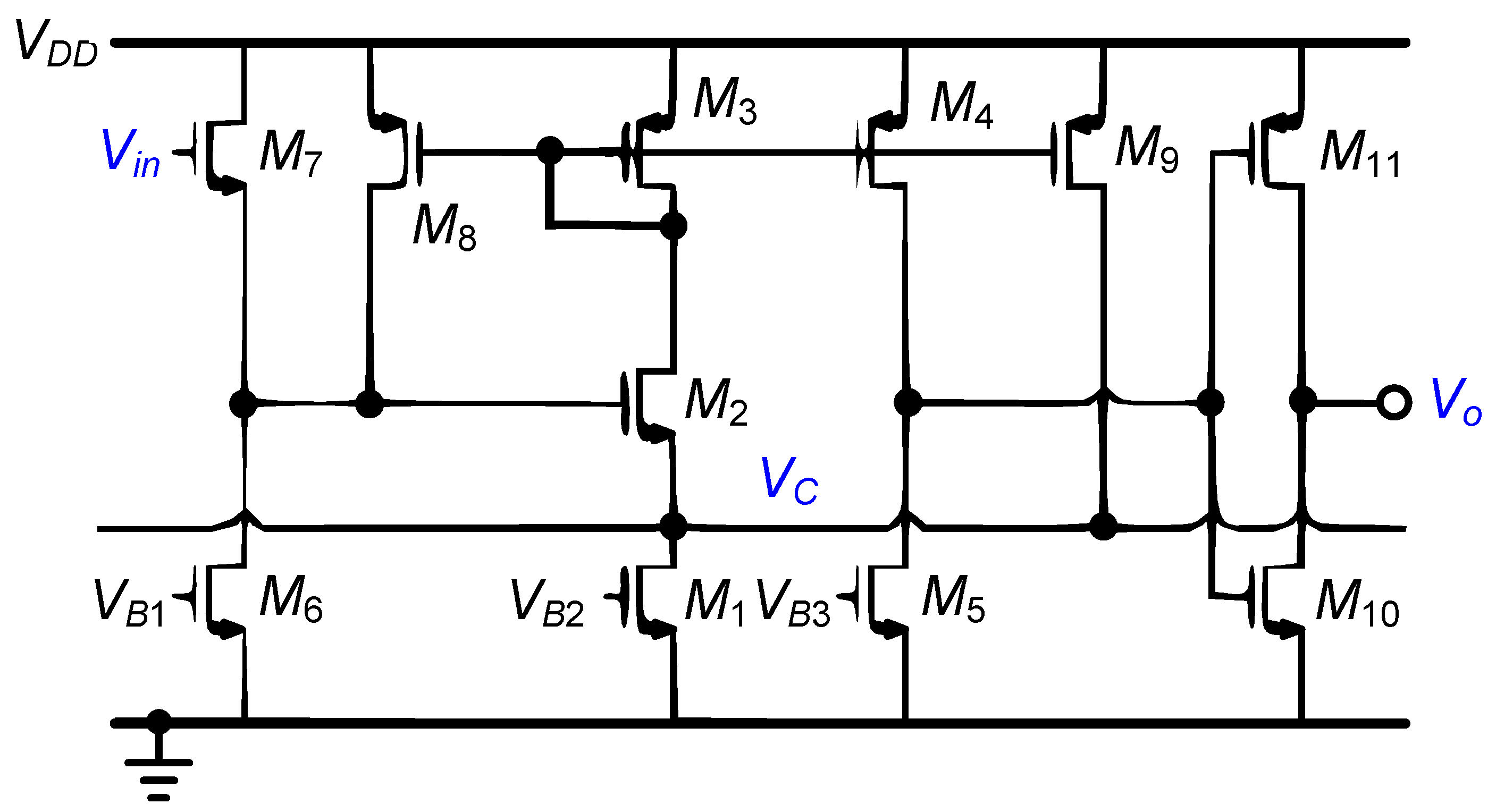
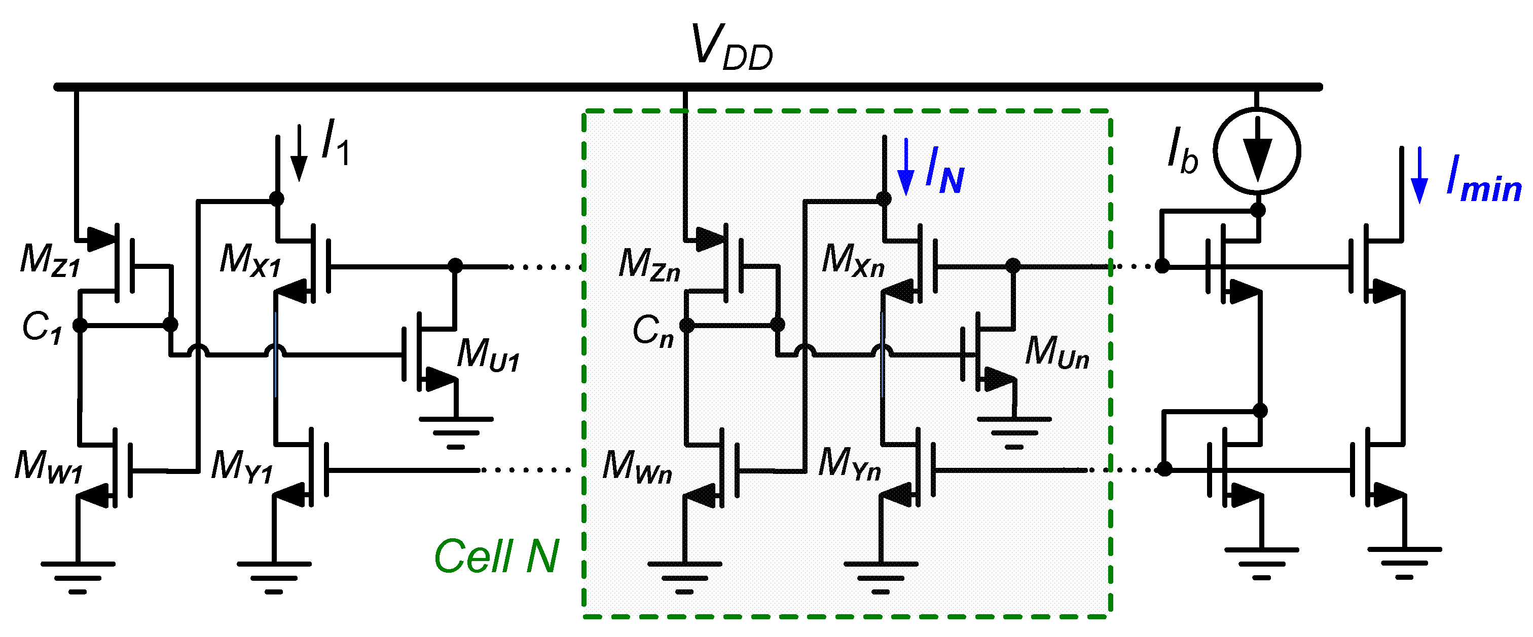
2.1. Current Conveyors

The current conveyor (CC) WTA circuit depicted in Figure 2 was originally proposed by Lazzaro et al. in [1]. Coined as Lazzaro’s circuit, the circuit is composed of N input cells in which the operation of all MOSFETs is in weak inversion. Every cell consists of a voltage follower (Mi2) and a common-source transistor (Mi1) in the form of a negative feedback loop. The voltage Vi at the input of Mi2 increases when the current Ii is greater than the rest. This enlarges the common voltage Vc and reduces the gate-source voltage (VGS) of all voltage followers except Mi2, switching off the corresponding devices as a result. The voltage Vc will eventually be proportional to the highest input, and the output current Io can be generated through Vc coupled to the gate of the output transistor (Mo). A problem of Lazzaro’s circuit is the presence of the interconnection parasitics, which slows down the operation. Another shortcoming comes from the reduced precision when increasing the number of identical cells for a lowered mismatch. Matching also trades with the device sizes and, consequently, the silicon area.
Several advanced implementations of WTA/LTA circuits are present in CMOS technology. A high-precision approach is introduced in [3] for improving the accuracy of Lazzaro’s circuit, aiming at processing more than 1024 inputs of a real-world scientific or industrial application. The circuit is capable of specifying the index of the winning signal as well as its value in the voltage domain. To describe its operation, it is worth noting that analyzing the inputs of this circuit is carried out by two layers. The voltages applied to a common voltage are converted to currents within the first layer, and the currents are used to generate a proportional voltage. The largest input significantly reduces other currents by raising the common voltage. The first layer is followed by the second layer, aiming at saturating the winning signal up to positive supply rail by enhancing the overall gain factor. In [9], each cell employs an auxiliary transistor cascaded with a sink current source, as illustrated in Figure 3, improving the resolution of Lazzaro’s circuit by enlarging the gain factor. By comparison, the voltage range is reduced in the presence of the transistor cascaded.
In ref. [13], the input currents are copied to NMOS and PMOS mirrors, as shown in Figure 4. The summation of the mirrored NMOS currents then flows into each cell to be compared with the inputs. The result of each comparison controls the output currents of the cells. This alters the total current flow into the current comparators, and the procedure continues until one current greater than the total one remains. The high-speed, high-precision WTA circuit reported in [14] incorporates an N-input current maximum selector in its input layer. The input stage produces N-current outputs, which are mirrored into a feedback circuit that produces the feedback current. The feedback current is used to correct the corner error of the maximum circuit. The output stage is formed by N high-speed current comparators that provide a binary output for each input. This way, only the output corresponding to the winning input will show a logical “1”. The solution in [20] contains inhibitory and excitatory feedback that prevent the selection of the potential winners. Each cell consists of 12 transistors connected to the common node Vc, according to the illustration in Figure 5. The input current is copied and compared with the average current of all cells. For the largest input, node Vx decreases such that its output exhibits a logical “1”. The inhibitory feedback decreases Vc of other cells, increasing Vx such that a logical “0” appears in their output. The excitatory feedback has an opposite impact on the winning signal. Node Vx of the winning cell is consequently reduced by increasing the input current. Since the input current is compared with the average of all inputs, the inhibitory and excitatory feedback will provide a hysteretic mechanism that prevents the selection of a potential winner unless it is stronger than the selection [20]. With a wide input current range, the above-described mechanism is well-suited for high-speed, high-precision applications.
The current-mode circuit developed in [21] is based on Lazzaro’s WTA circuit, seeking to increase the accuracy in low-voltage environments. As depicted in Figure 6, each input voltage follower in the original circuit is replaced by a flipped voltage follower or FVF. An FVF is essentially a voltage follower (MAi), which includes a negative shunt feedback (via MCi), enabling the sink of large currents by keeping constant the voltage of the current sensing device. All the FVF cells are coupled to a low-impedance common Vc. The implementation is essentially a maximum current selector since its output current Io follows the maximum between I1 and In. Its main advantage is the modest VGS+2Vov supply voltage requirement, in which Vov is the transistors’ overdrive voltage.
Proposed in [25], the current-mode LTA solution in Figure 7 includes MoA as a voltage-controlled current source, with node U common for all MiA devices. Within each cell, MiC converts the input current Ii into a proportional drain voltage. The source-to-gate voltages of MiB compete at node U, and the maximum voltage corresponding to the smallest input current is considered the winner [25]. The architecture is simple, low-power, and modular.
In ref. [27], a voltage-mode WTA is developed with excitatory and inhibitory feedbacks based on the original WTA core in [3]. Figure 8 shows the scheme of the WTA cells, including which M8 and M9 constitute the excitatory and inhibitory circuits, respectively. The additional feedback enhances the resolution without introducing any extra stage.
Another voltage-mode simple architecture for detecting the maximum and minimum inputs is reported in [32]. Its tiny size with a minimum number of transistors makes it ideal for high-frequency applications. The circuit combines the differential amplification with shunt feedback in the voltage buffer, in which the output voltage follows the winning input, although its address is not specified. The solution proposed in [34] utilizes a common-gate transistor to enhance its open-loop gain factor. High accuracy levels can thus be reached in low-voltage environments. Figure 9 exhibits the current-mode LTA circuit proposed in [38]. The role of the triode Mwi in each cell is to establish an effective feedback mechanism. The minimum input current generates the largest voltage at Ci, and the relevant Mui sinks current from Ib so as to copy the lowest input current to the output. High-speed operation can be reached with high accuracy levels at the expense of more power consumption and area. The minimum voltage supply is also increased because of cascade current mirrors.
Figure 10 presents another derivation of Lazzaro’s circuit with speed and accuracy advantages [37]. The output impedance at node Vc is decreased by the additional feedback loops through Mi3. The circuit shows superior performance with respect to the original Lazzaro’s circuit. However, power consumption and area are increased because of more branches.

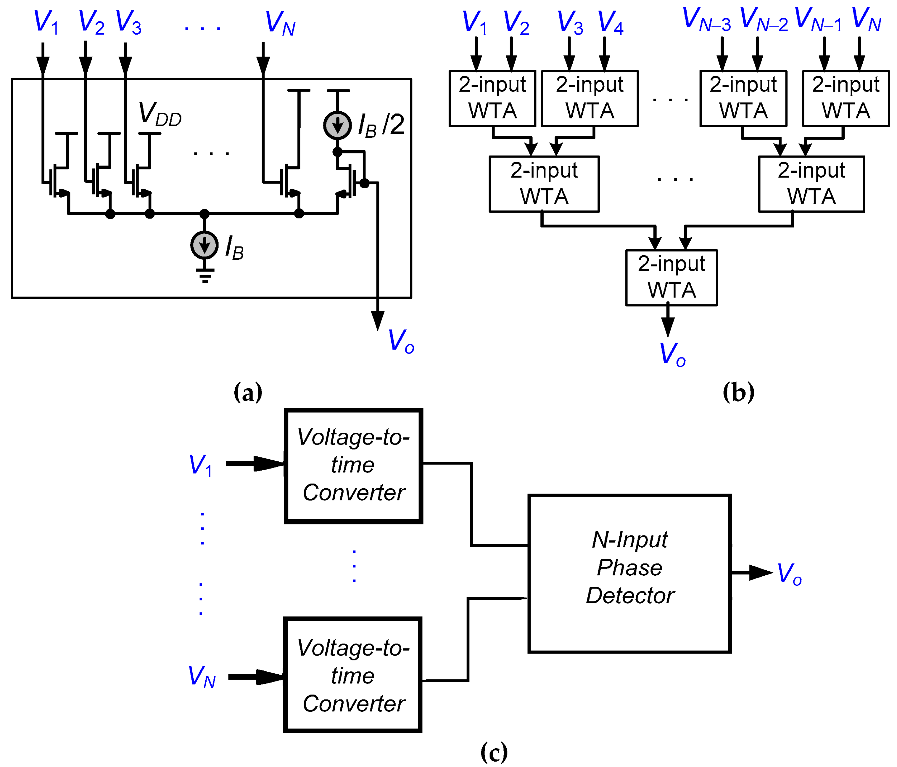
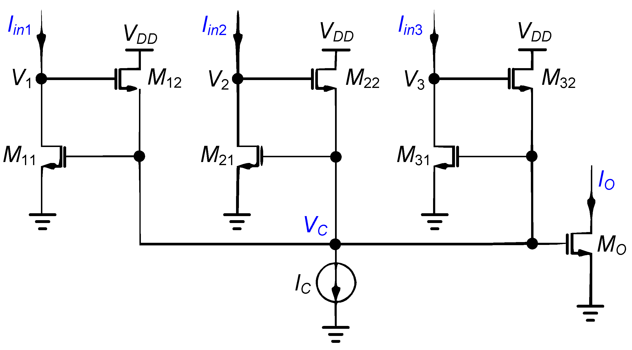
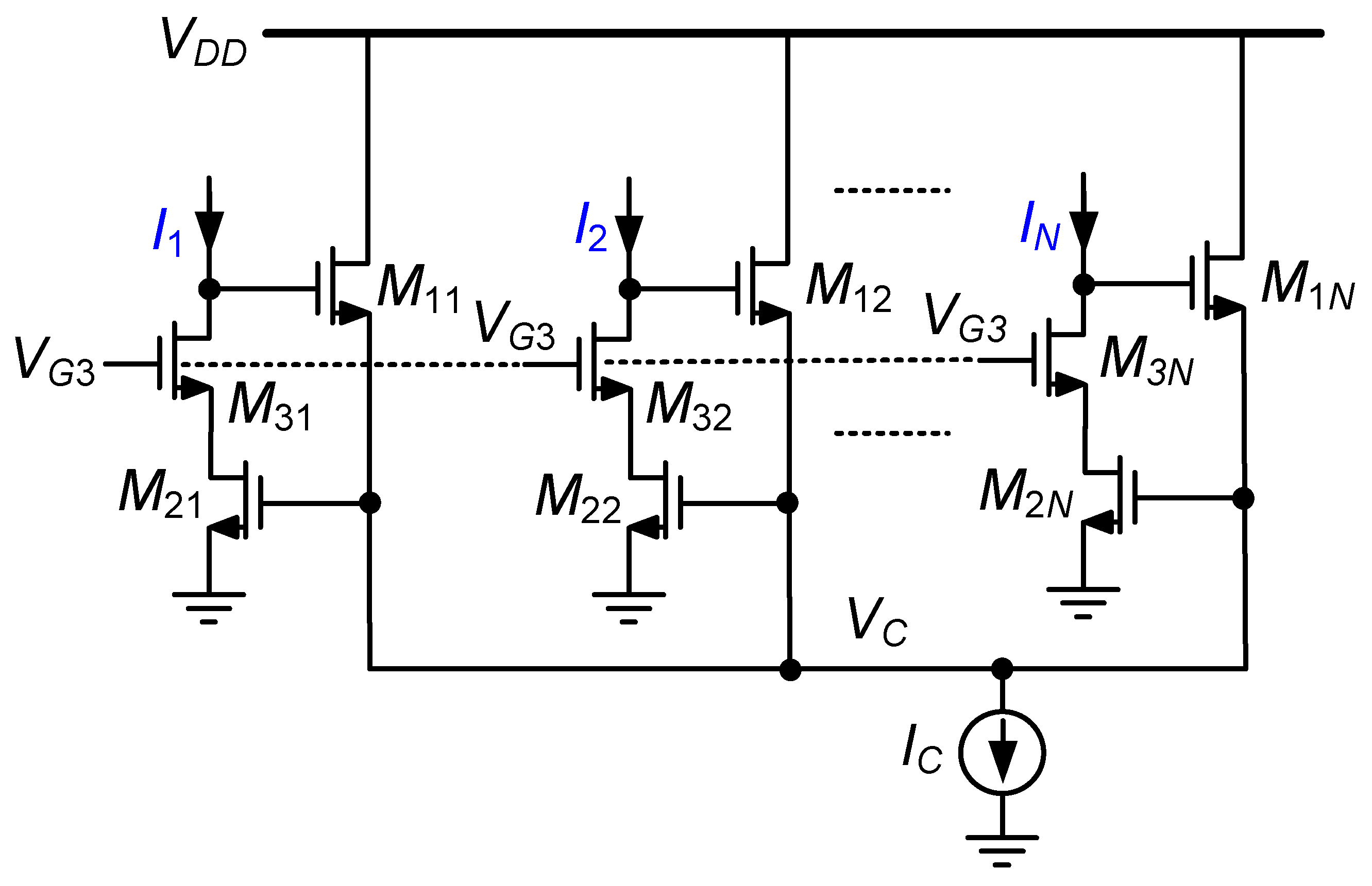
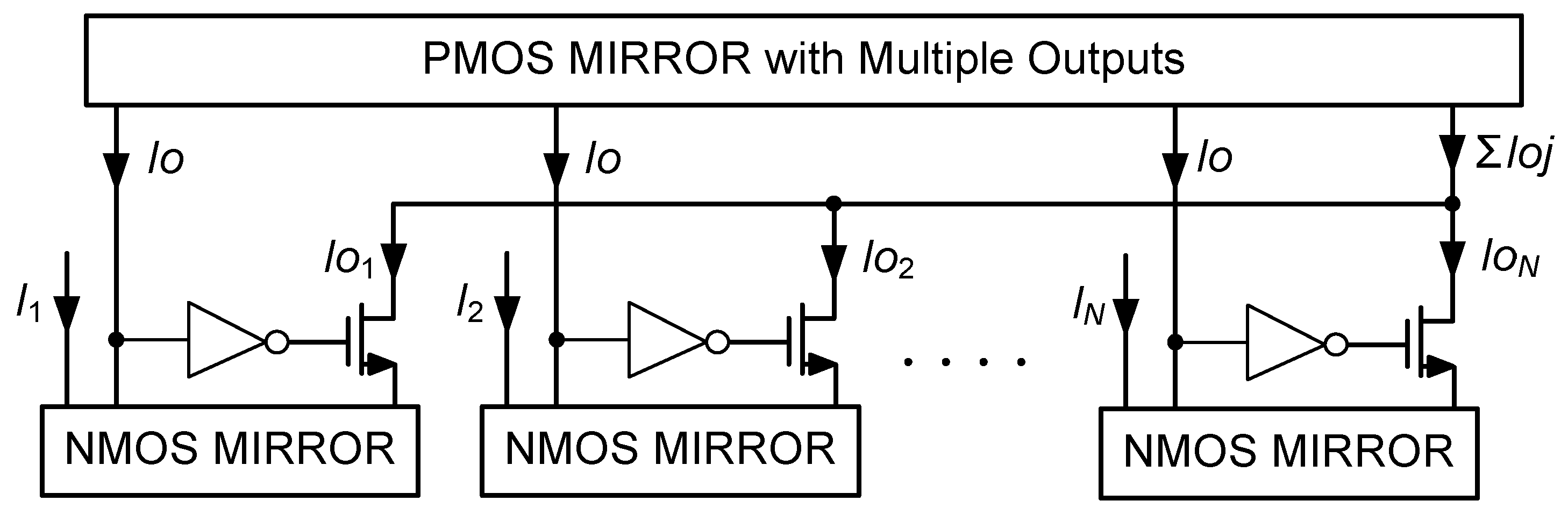
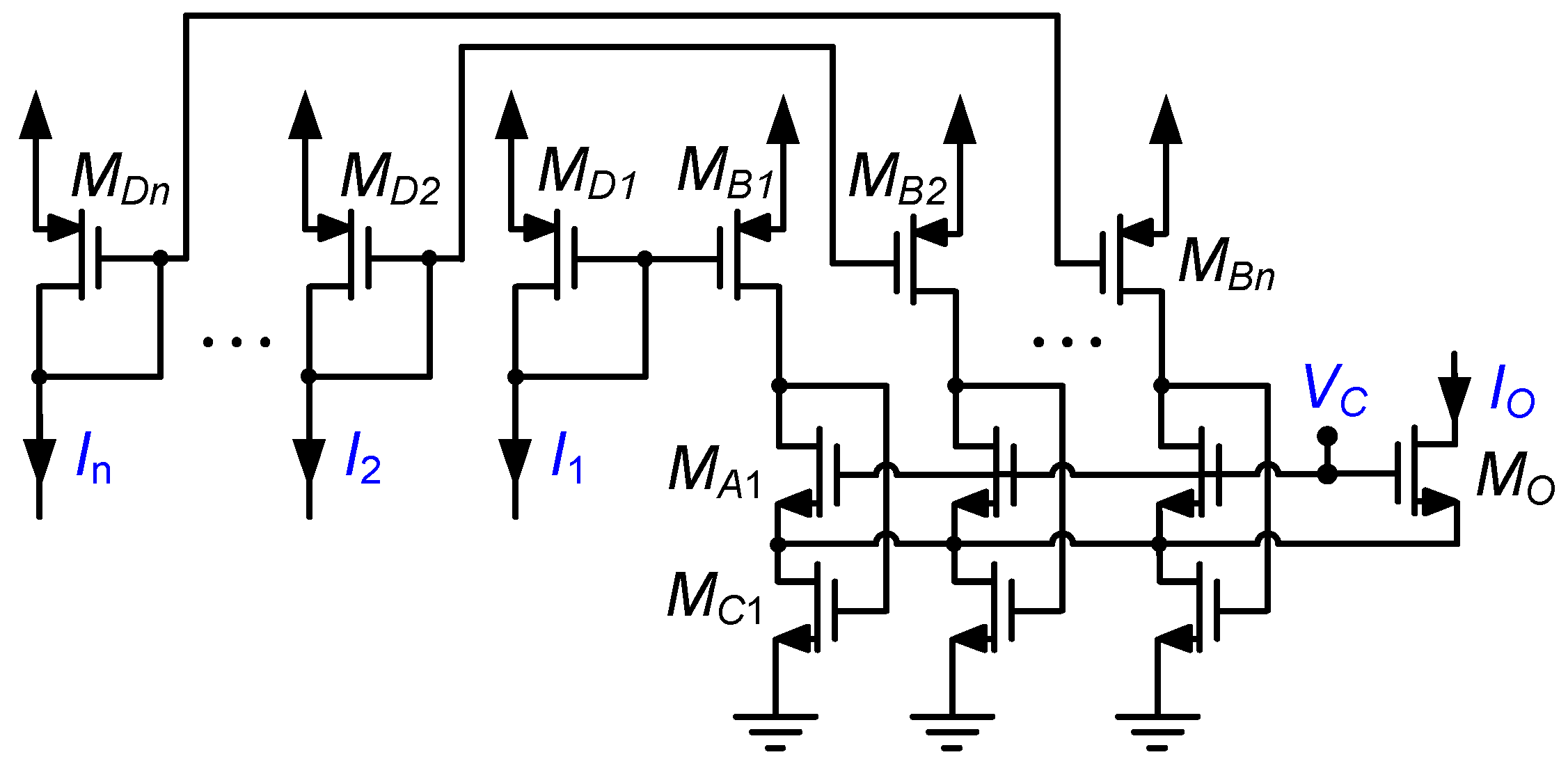
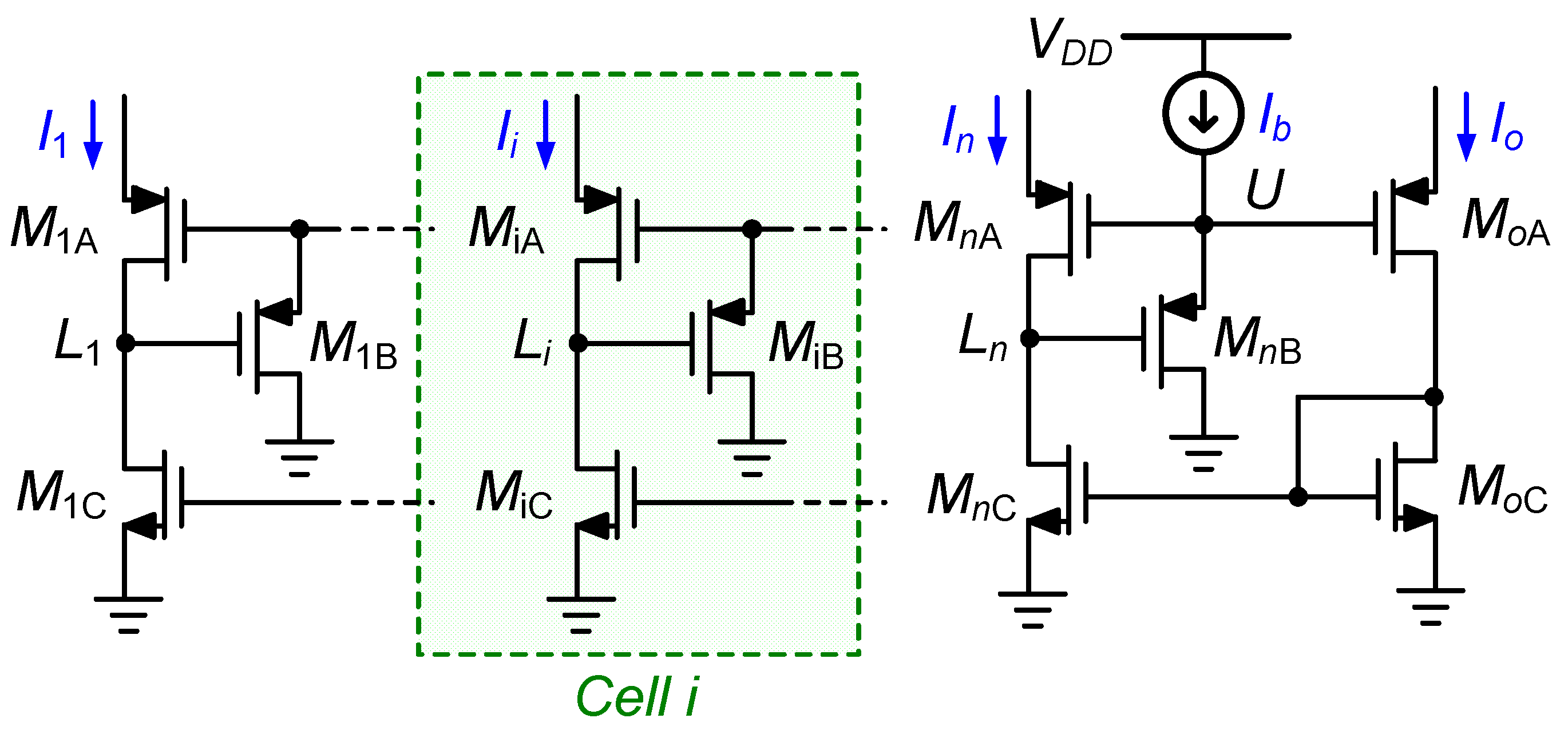
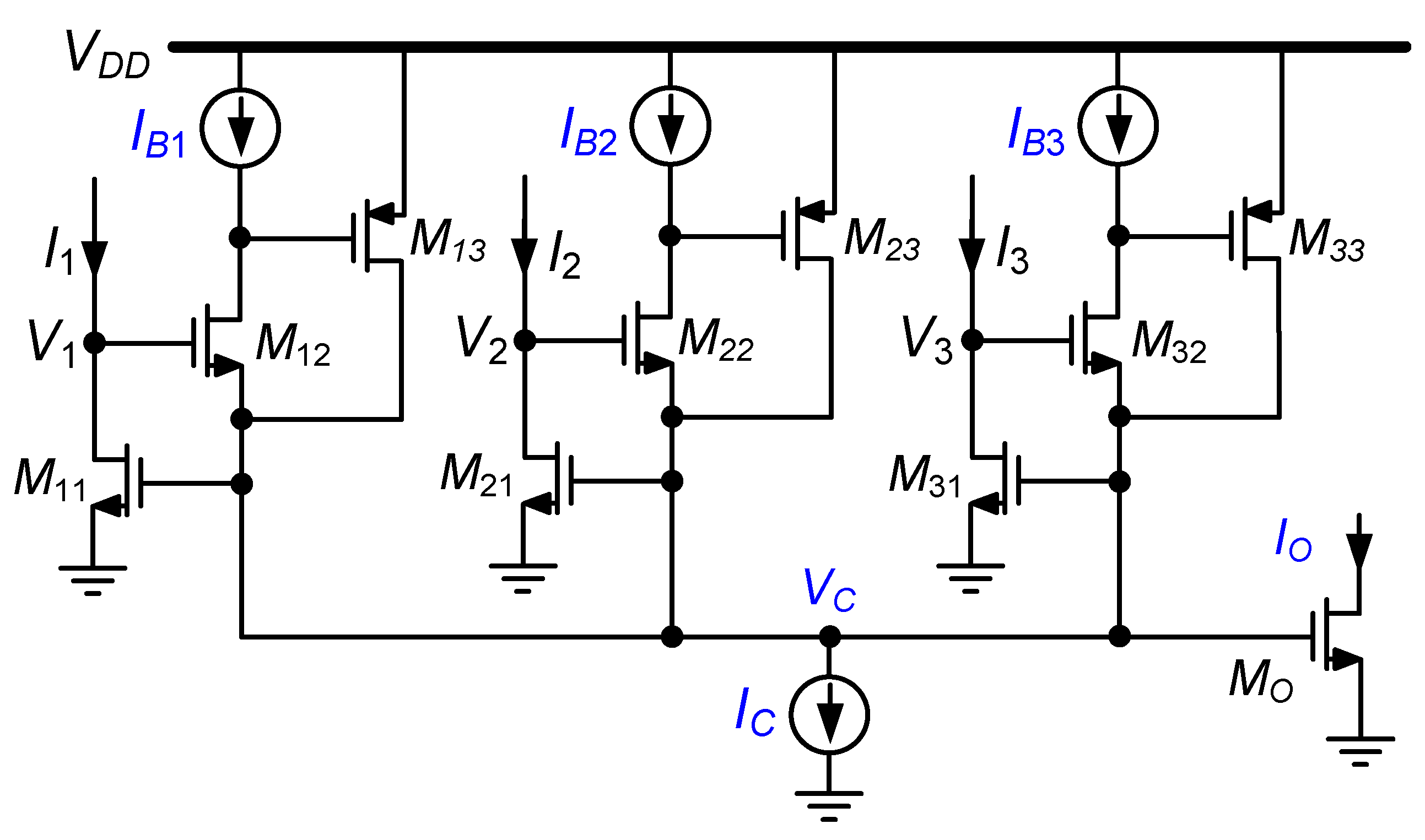
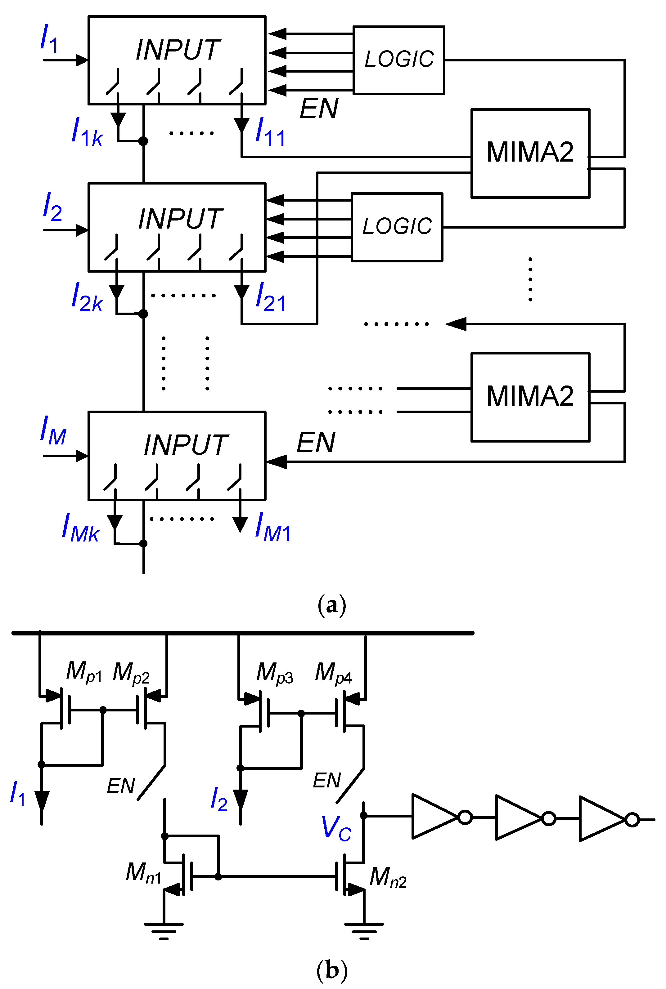
2.2. Binary Tree WTA Circuits

The input signals of the BT topologies are coupled in pairs, and one signal out of each pair is only considered a local winner. The winner takes part in the competition of the next layer until the global winner is specified. Increasing the number of inputs does not affect the accuracy of BT topologies. Nevertheless, the area, power, and delay are increased. During the 90′s decade, binary-tree WTAs were used widely in applications such as nonlinear filters, analog-to-digital converters, vector quantizers, and fuzzy circuits [2,4,6,10]. The voltage-mode binary-tree WTA in Figure 11 is presented In [17]. The initial comparison is fulfilled between two random inputs. The greater input voltage is directed to the output, and a digital output is preserved for its address. The output of the first stage is then applied to the second stage for comparison. This procedure continues iteratively until the largest input is determined with its address.
Another current-mode WTA presented in [23] can operate at low supply voltages down to 0.5 V. The circuit is composed of a transresistance comparator and a few current mirrors and is utilized for learning Kohonen’s network. Figure 12 illustrates another binary-tree WTA developed in [26]. It consists of the front-end current-to-time converters prior to the time comparators. The input currents are converted to time delays (a delayed pulse in which the delay is proportional to the input), and the time comparators compare the input delayed pulses. The larger inputs are then determined and directed to the next layer, enabling us to finally determine the largest input current. The main advantages of this circuit are its low-power and low-voltage operation. However, speed is a challenge for the described topology.
In ref. [29], a translinear loop is utilized to amplify the difference between the two inputs prior to comparison. A positive feedback loop is also used to improve the comparison accuracy. The operation of its transistors in the sub-threshold region not only reduces its consuming power but also enhances the precision as compared to the early solutions. However, similar to other BT circuits, speed is a challenge. Another current-mode binary-tree WTA circuit is presented in [28], where a modified current comparator and mirroring scheme are exploited to improve both latency and accuracy. As shown in Figure 13a, a block denoted by MIMA2 (Figure 13b) is used to compare the input currents in this solution. The main idea is to stimulate MIMA2 such that it sends information regarding the winning signal through the LOGIC block back to the INPUT block. In response, the input block passes another copy of the winning signal to the next layer. This architecture benefits from less propagation delay.
Other binary-tree WTA/LTA topologies have been introduced for spiking neural networks (SNN) or neuromorphic applications [42,44], which suffer from excessive delay and larger are as and will not be described here for the sake of brevity.

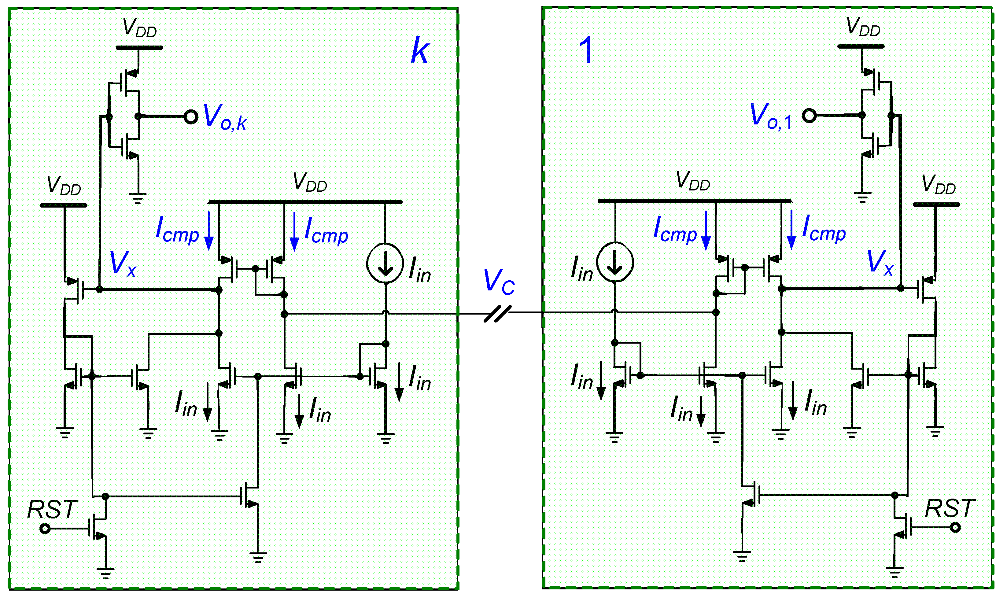
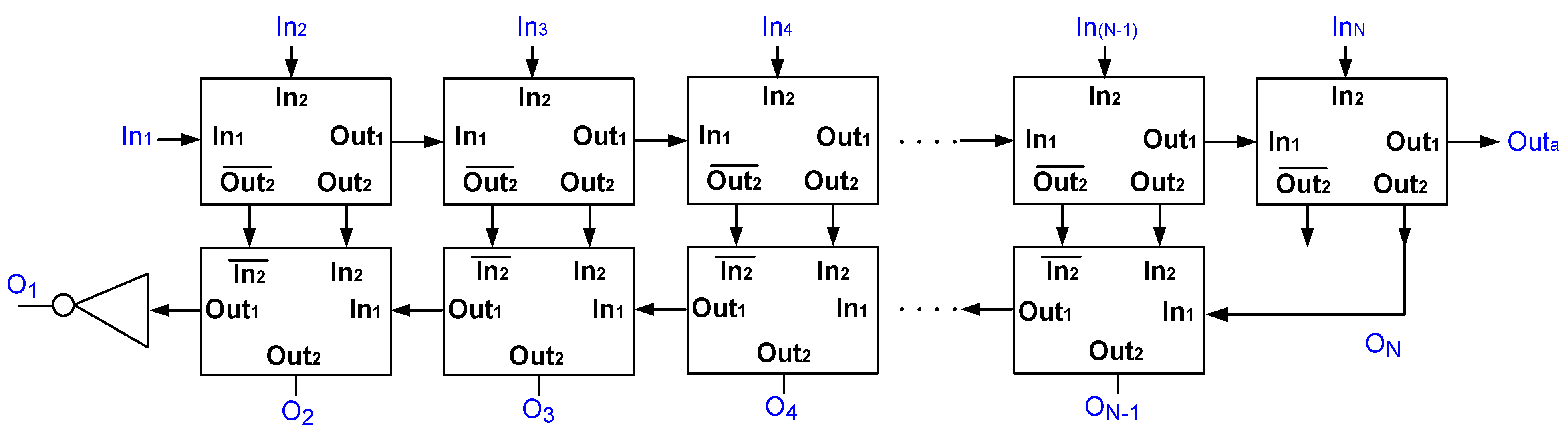
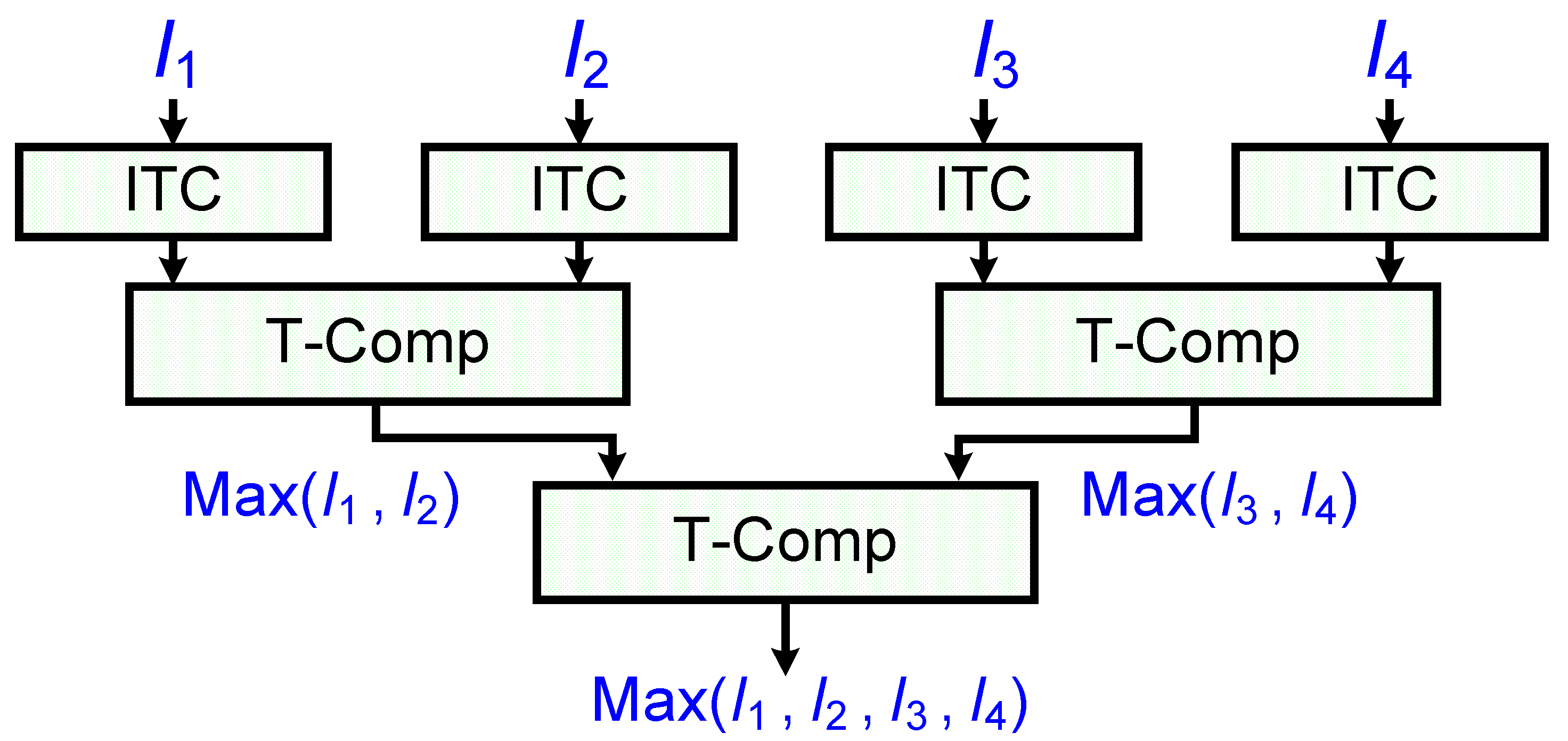
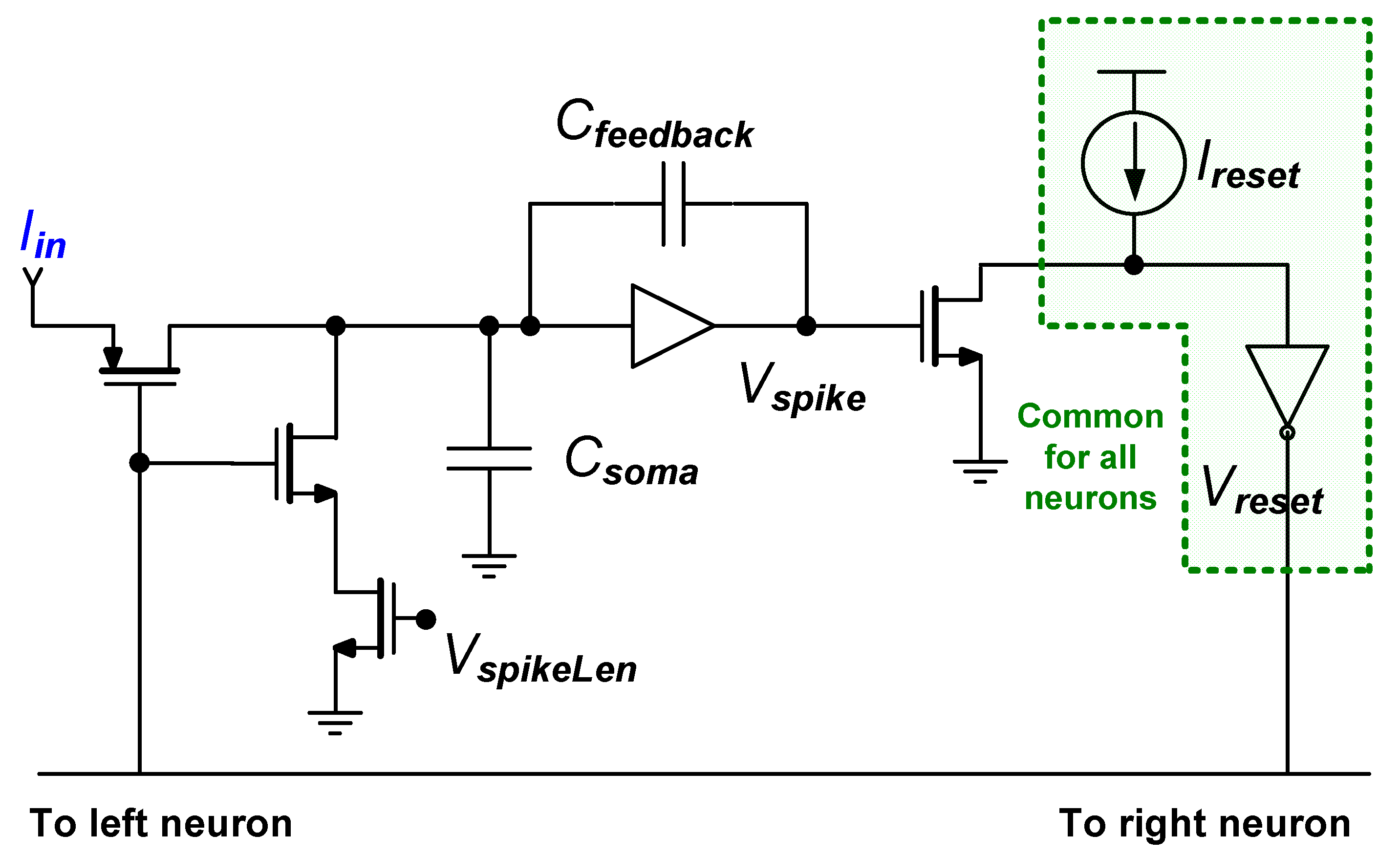
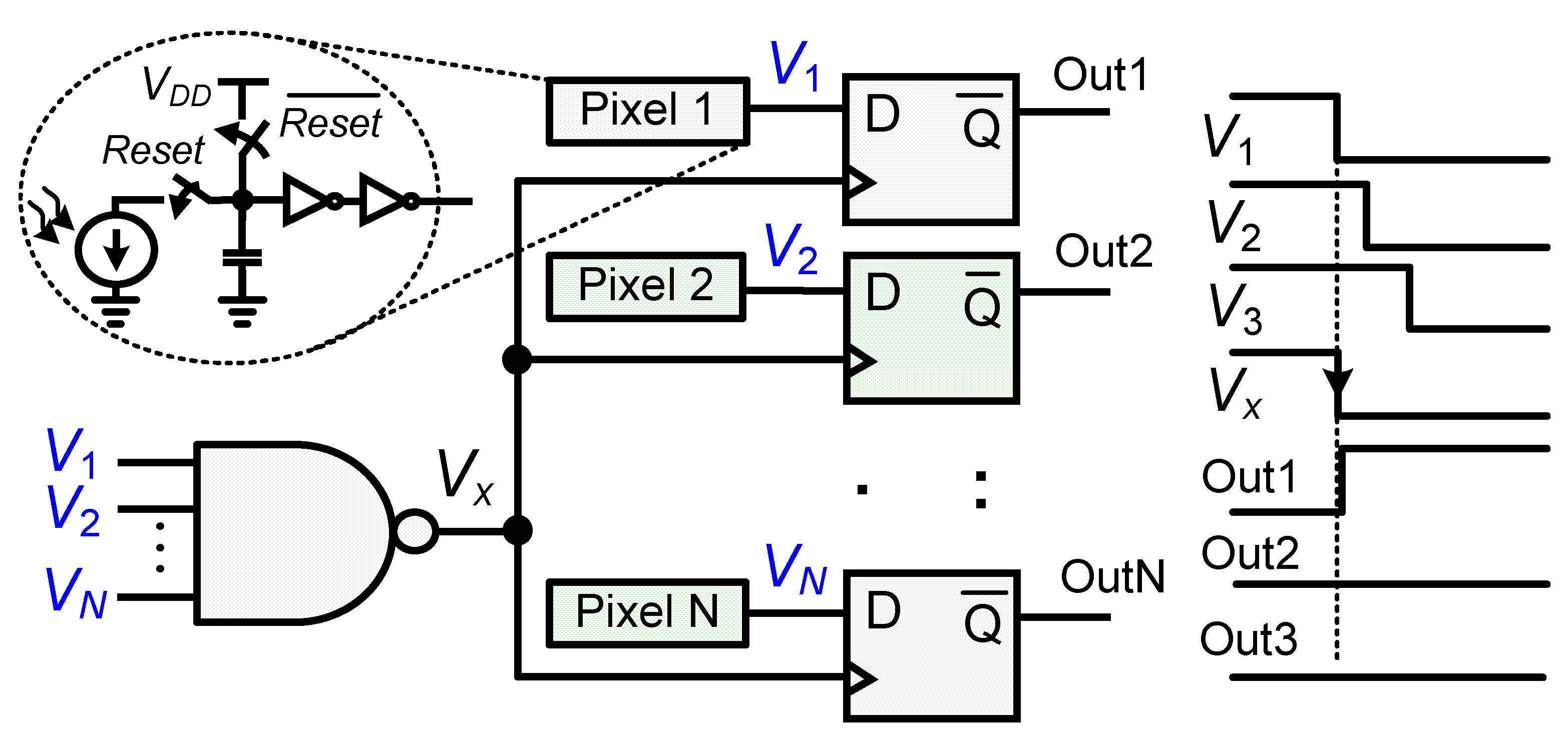
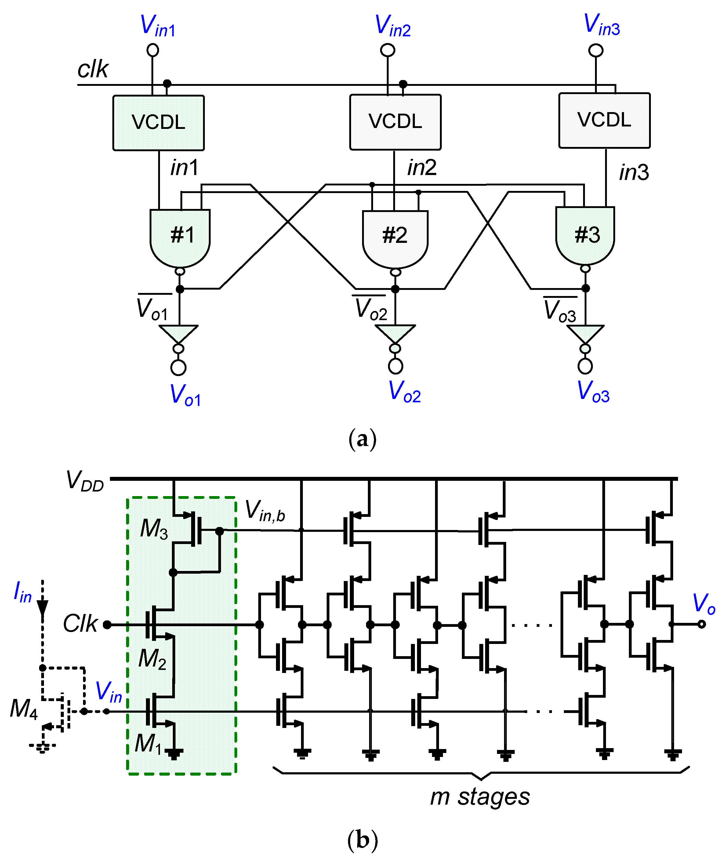
2.3. Time-Domain WTA/LTA Circuits

Time-domain solutions are becoming more popular due to their compatibility with low-voltage CMOS technology. A number of time-domain WTA configurations have been reported in the literature [12,33,48,49]. The recent time-domain configurations are becoming comparable with the class of CC and BT solutions in terms of speed, power, and resolution. The first time-domain WTA circuit to be discussed in this section is based on the self-resetting integrate-and-fire neurons [19]. Each neuron functions as a WTA cell, according to Figure 14. The internal capacitor (Csoma) is charged by the input current of the cell. The larger the current, the faster the capacitor charging will be. The first neuron, which reaches the threshold switching voltage of the inner inverter, pulls up the output and generates an output spike. The first spike thus resets other cells and causes zero outputs until the next sampling time. Large capacitors are needed for this circuit to reach higher resolutions, which affects its speed.
A similar approach was applied in [35] for imaging. The capacitor is precharged in every pixel of the image sensor, as shown in Figure 15. The pixel capacitor is then discharged by a current source that depends on the intensity of the incident light. Two inverters are used to detect the timing at which the capacitor voltage reaches the threshold voltage VDD/2. As such, the input signals of the D-type flip flops (DFFs) and NAND gates (V1, V2, ..., VN) would be the digital pulses with different delays. As soon as the output of the pixel of the winning current becomes Low, the output of the NAND gate pulls down, and all DFFs are clocked at the falling edge of Vx. The DFF output corresponding to the winner thus changes to High while the rest remain Low. Using an open-loop structure for comparing the input-dependence delay times lowers the resolution of this circuit. For instance, when two input currents are close, the phase detector will not be able to detect the first pulse. Non-unique winners may also occur when more than one output becomes High.
The combination reported in [43] is meant for the learning engine of the neural networks based on a parallel activity. In each cell, a linear delay element is used for converting the input voltage to a delayed pulse. A sensing amplifier is then utilized to detect the winning pulse corresponding to a larger input voltage. The time-domain WTA circuit illustrated in Figure 16a is presented in [47]. Here, the input signals control a reference clock pulse within the voltage-controlled delay lines (VCDL). The implementation of VCDL blocks is depicted in Figure 16b. The delays corresponding to the inputs are proportional to the number of VCDL stages (N). Hence, it is possible to customize the value of N based on the required resolution. Conceptually, the delays corresponding to the inputs are amplified by VCDLs, and the positive-feedback phase detector detects the first pulse and deactivates other outputs. Amplification of time through VCDLs also enhances the resolution. Other advantages of this circuit are high-speed, low-power, and low-voltage operations. Despite these advantages, it suffers from the limit of input common-mode voltage. Specifically, at least one input voltage must be greater than anNMOS threshold voltage, which is critical for low-voltage operation. The area is also increased for high-resolution applications.

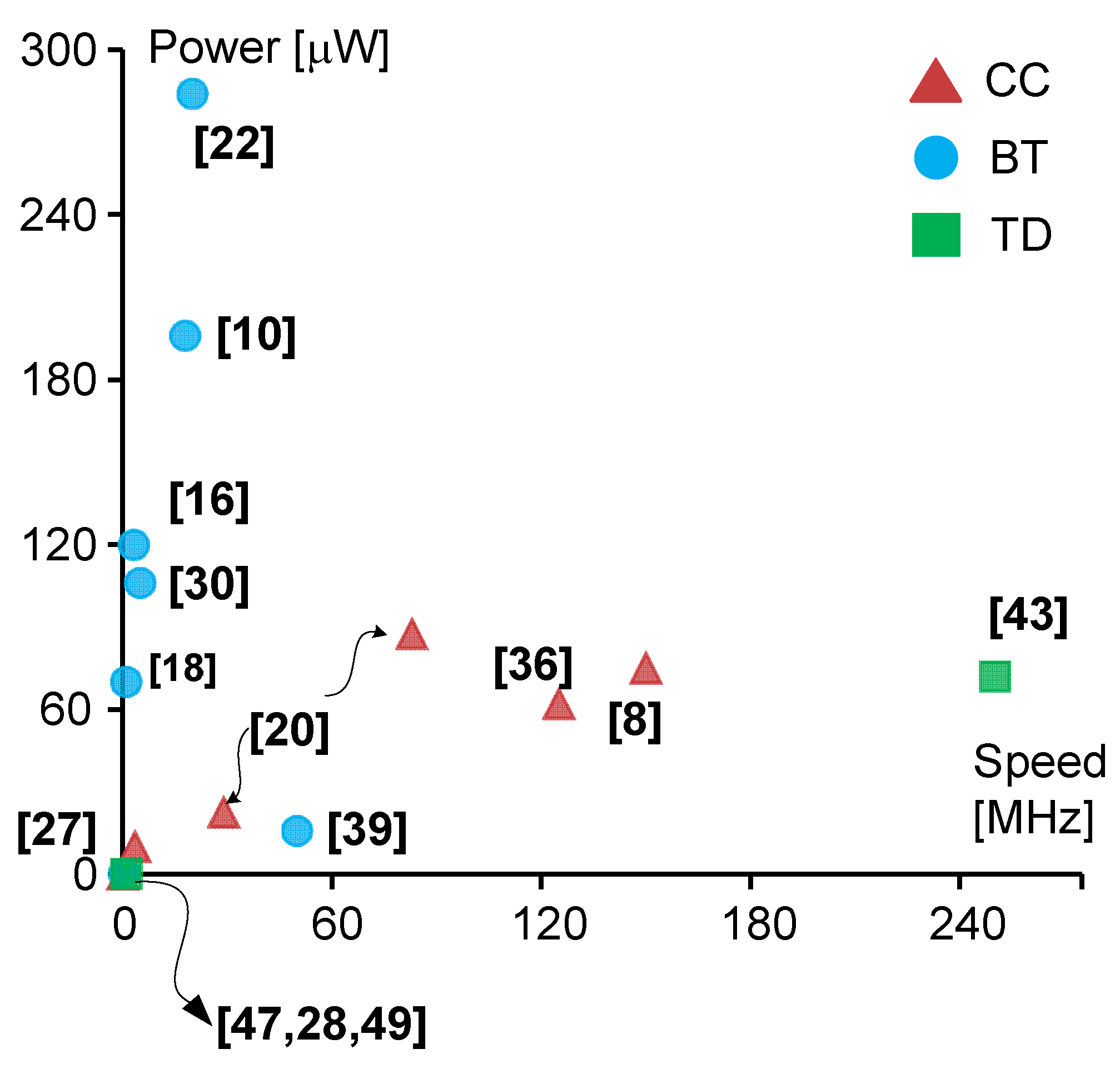
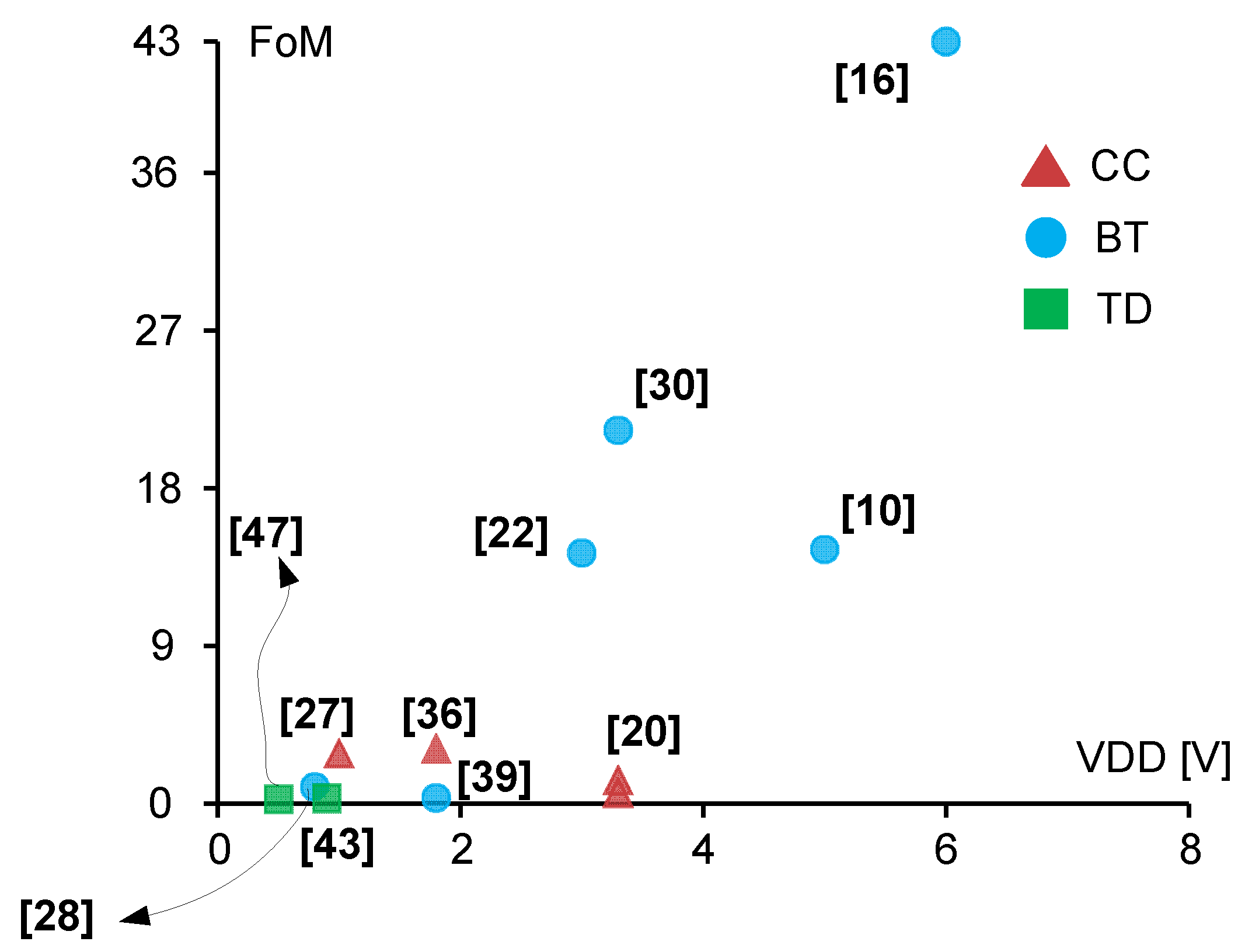
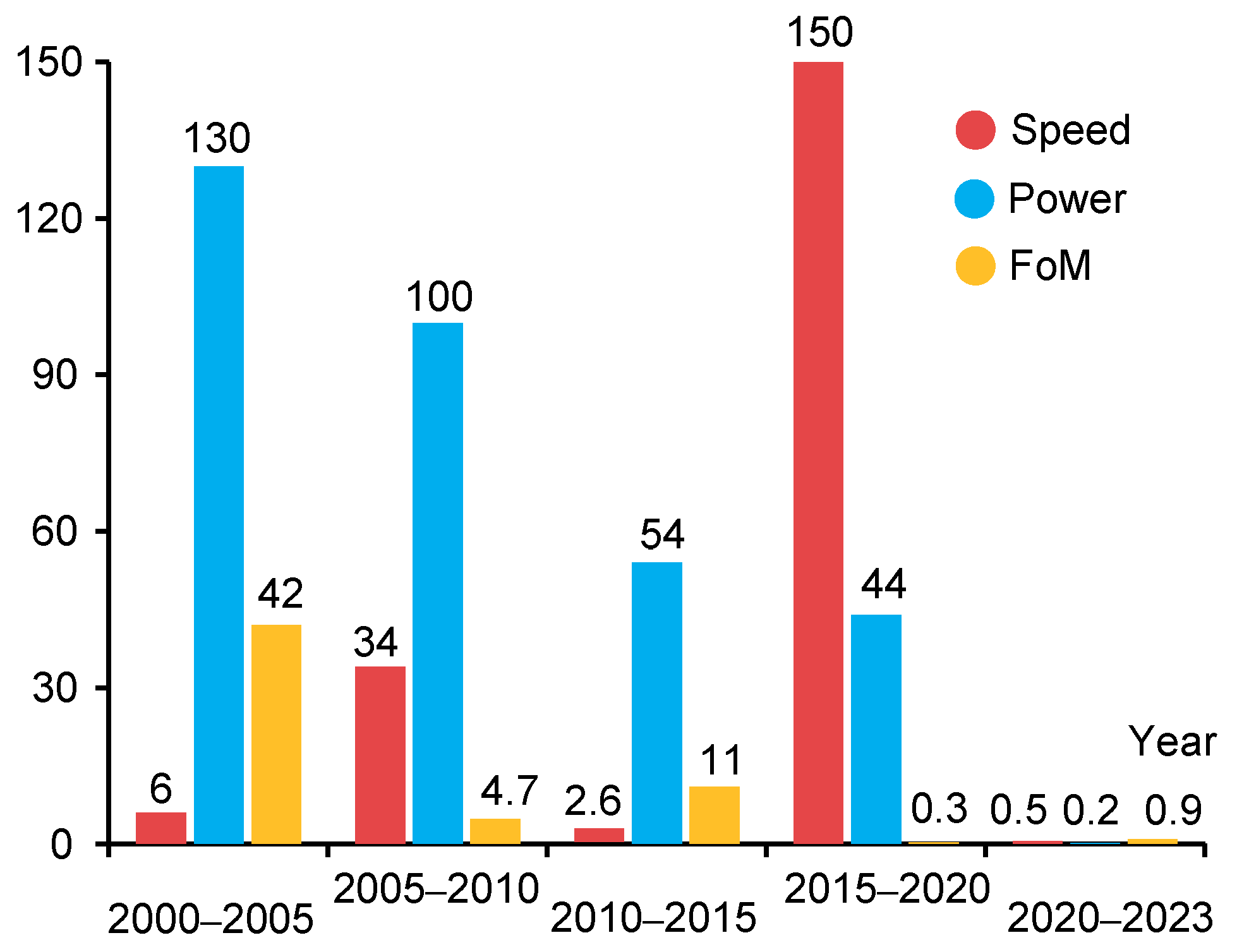
3. Comparison and Discussions

The performance of WTAs/LTAs can be compared from various perspectives. Resolution, power, area, speed, complexity, supply voltage range, compatibility with CMOS technology, and the number of inputs should be accounted for in a fair comparison. Most of the circuit improvements of WTAs/LTAs were reviewed in the previous section. At first, a general comparison will be made between the three WTA/LTA classes. It should be noted that the forthcoming results are based on the data reported in the original publications and not on a new design phase. Figure 17 compares the speed and power of the CC, BT, or TD configurations. CC topologies not only achieve higher speeds but also can lower power consumption. By comparison, BT architectures can reach better accuracy levels at the price of inferior speed and more power consumption caused by more internal layers. Very little data are available about the time-domain WTAs. Nonetheless, low power and medium speed can be expected from these architectures. From the accuracy point of view, BT topologies have a significant preference. The ability to process many inputs also increased the demand for the corresponding implementation in recent years. Overall, both CC and BT circuits found their particular applications, depending on the advantages such as speed, area, power or accuracy/precision, number of inputs, and reliability of one category over the other. The main advantage of TD design is its flexibility for different applications. Not only can these architectures be part of a low-power and low-voltage design, but their technology compatibility and digital nature make them ideal for medium-frequency and high-resolution applications.
The following Figure-of-Merit (FoM) is utilized to quantify the operation of different WTA/LTA solutions [8,21]:
F o M = P o w e r f × N
where N and f refer to the number of inputs and maximum operating frequency, respectively. The viewpoint of low-voltage operation, the circuits presented in [28,43,47,48] are more promising, while the implementation presented in [43] has a relatively higher operating frequency. On the other hand, the TD circuit reported in [47] exhibits a lower voltage operation and, thus, a superior FoM.
In terms of speed, the circuits in [20,43] show better metrics. The configuration in [43] is capable of operating with a large number of inputs. As a result, it exhibits better FoM, whereas the circuit in [20] is compact and more accurate. In terms of accuracy, excellent results have been reported in [20,28,33,38,47]. The binary-tree structure is superior since it only compares two inputs simultaneously. This advantage is more prominent when the number of inputs is increased at the cost of more power consumption and lower speed. Current conveyor and time-domain WTA circuits can obtain different accuracies depending on their implementation, but the power consumption of the time-domain structures is superior, besides no stability issues.
As it is evident, the precision of a binary tree WTA is independent of its number of inputs. Analytically, we can hence claim that the precision of the BT topologies surpasses other implementations, especially for an increased number of inputs. Nonetheless, the calculation of the precision is mostly ignored and not carried out in the literature. To sum up, this claim is analytically reasonable, although little data are available to prove it statistically. From the perspective of power consumption, [28,47,49] can reach the lowest power per cell, but [28,47] show better resolution and FoM. Regarding the area occupied, CC-based topologies occupy the least area as compared with BT circuits. Exceptionally, the TD WTA circuit reported in [47] shows a comparable area. Table 1 presents a comprehensive comparison between the main WTAs presented in the prior art. The highest performance metrics belong to [28,43,47]. Regardless of the architecture, both the technology node and supply voltage strongly affect the operation of WTA/LTA circuits. In our comparison table, there exist a number of old structures with outdated technologies (0.5–2.4µm). Presenting the early studies in this review was only to investigate the trend of WTA/LTA design. However, similar to any other fields, the primitive WTA/LTA configurations suffer from more complexity, poor efficiency, and high consumption of power and silicon footprint. Most of the early solutions cannot even be realized under the reduced supply voltage of nano-scale technologies. From a technology point of view, the main issues are speed, power, and supply voltage. Circuit design in new technologies benefits from high speed and less silicon area. However, there are some challenges, such as leakage current, more cost, and more complexity. To choose the appropriate technology, if high speed is not required, using older process nodes with supply voltage lower than nominal is a good choice. This can reduce both power consumption and manufacturing costs simultaneously. However, the area will increase. In those high-speed circuits in which the power consumption is not the issue, choosing the new technology nodes is thus suggested. However, it should be kept in mind that older architectures cannot be implemented at low supply voltage in the presence of more stacked transistors. Finally, since speed and precision are traded, it will be difficult to choose a technology for a high-precision design. However, despite the technology compatibility of the time-domain WTAs, this solution is more suited for precise implementation.
Figure 18 summarizes the FoM vs. supply voltage of those circuits reported in Table 1. From these results, it can be concluded that the operating voltage can be related to the technology scaling. Also, technology scaling does not improve the performance of CC architectures. This was expected since most of these circuits are analog. Another point from Figure 18 is that the performance of BT circuits is improved almost linearly with scaling. This is because of the digital nature of these structures.
Generally, there are three types of applications for the WTA/LTA circuits. The first type is that set of applications that call for high speed and high resolution with a smaller number of inputs. The second type is those implementations that need precision/accuracy despite the large number of inputs. The third application requires very compact and high-speed circuits with medium resolution and a large number of inputs. Figure 19 gives a full statistical view of the circuits presented in recent years. The average speed of the WTAs has been increasing in the past decades. In contrast, the consumption power and FoM show a significant reduction. This is mainly by virtue of technological improvement and more demand for low-power and high-frequency applications.

4. Conclusions

In this review, we presented an overview of the present WTA/LTA solutions to help improvise the proper solutions for future designs. At first, we briefly reviewed the research works published on different designs and their applications over the past decades. Classifications of the present WTA/LTA architectures were presented later. The main advantages and disadvantages of each CC, BT, and TD topologies were also described. Specifically, power consumption, speed, resolution, area, number of inputs, and low-voltage operation were studied and compared.

Author Contributions

Conceptualization, E.R.; writing—original draft preparation, E.R.; supervision, H.A.; writing—review and editing, H.A. All authors have read and agreed to the published version of the manuscript.

Funding

This research received no external funding.

Institutional Review Board Statement

Not applicable.

Informed Consent Statement

Not applicable.

Data Availability Statement

The data are available upon request from the corresponding author.

Conflicts of Interest

The authors declare no conflict of interest.

References

  1. Lazzaro, J.; Ryckebusch, S.; Mahowald, M.A.; Mead, C.A. Winner-Take-All Networks of O(N) Complexity; Defense Technical Information Center: Fort Belvoir, VA, USA, 1988. [Google Scholar]
  2. Sasaki, M.; Inoue, T.; Shirai, Y.; Ueno, F. Fuzzy multiple-input maximum and minimum circuits in current mode and their analyses using bounded-difference equations. IEEE Trans. Comput. 1990, 39, 768–774. [Google Scholar] [CrossRef]
  3. Choi, J.; Sheu, B.J. A high-precision VLSI winner-take-all circuit for self-organizing neural networks. IEEE J. Solid-State Circuits 1993, 28, 576–584. [Google Scholar] [CrossRef]
  4. Tuttle, G.T.; Fallahi, S.; Abidi, A.A. An 8 b CMOS vector A/D converter. In Proceedings of the 1993 IEEE International Solid-State Circuits Conference Digest of Technical Papers, San Francisco, CA, USA, 24–26 February 1993. [Google Scholar]
  5. Le Nguyen, B.; Hock Choong, C. A neural-network contention controller for packet switching networks. IEEE Trans. Neural Netw. 1995, 6, 1402–1410. [Google Scholar] [CrossRef] [PubMed]
  6. Smedley, S.; Taylor, J.; Wilby, M. A scalable high-speed current-mode winner-take-all network for VLSI neural applications. IEEE Trans. Circuits Syst. I Fundam. Theory Appl. 1995, 42, 289–291. [Google Scholar] [CrossRef]
  7. Gunay, Z.S.; Sanchez-Sinencio, E. CMOS winner-take-all circuits: A detailed comparison. In Proceedings of the 1997 IEEE International Symposium on Circuits and Systems (ISCAS), Hong Kong, China, 12 June 1997; pp. 41–44. [Google Scholar]
  8. Pouliquen, P.O.; Andreou, A.G.; Strohbehn, K. Winner-Takes-All Associative Memory: A Hamming Distance Vector Quantizer. In Neuromorphic Systems Engineering; The Springer International Series in Engineering and Computer Science; Springer: Boston, MA, USA, 1998; pp. 437–456. [Google Scholar] [CrossRef]
  9. Sekerkiran, B.; Cilingiroglu, U. Improving the resolution of Lazzaro winner-take-all circuit. In Proceedings of the International Conference on Neural Networks (ICNN’97), Houston, TX, USA, 12 June 1997. [Google Scholar]
  10. Demosthenous, A.; Smedley, S.; Taylor, J. A CMOS analog winner-take-all network for large-scale applications. IEEE Trans. Circuits Syst. I Fundam. Theory Appl. 1998, 45, 300–304. [Google Scholar] [CrossRef]
  11. Dobrescu, D.; Comanescu, R.; Dobrescu, L. Neuron MOS technique designed 8 channels Winner Takes it All integrated circuit. In Proceedings of the 1998 International Semiconductor Conference. CAS’98 Proceedings (Cat. No.98TH8351), Sinaia, Romania, 6–10 October 1998. [Google Scholar]
  12. Opris, I.E. Rail-to-rail multiple-input min/max circuit. IEEE Trans. Circuits Syst. II Analog Digit. Signal Process. 1998, 45, 137–140. [Google Scholar] [CrossRef]
  13. Serrano-Gotarredona, T.; Linares-Barranco, B. A high-precision current-mode WTA-MAX circuit with multichip capability. IEEE J. Solid-State Circuits 1998, 33, 280–286. [Google Scholar] [CrossRef]
  14. Vlassis, S.; Siskos, S. High speed and high resolution WTA circuit. In Proceedings of the ISCAS’99. 1999 IEEE International Symposium on Circuits and Systems VLSI (Cat. No.99CH36349), Orlando, FL, USA, 30 May–2 June 1999. [Google Scholar]
  15. Zhang, Y.; Pheng-Ann, H.; Ping-Fu, F. Winner-take-all discrete recurrent neural networks. IEEE Trans. Circuits Syst. II Analog Digit. Signal Process. 2000, 47, 1584–1589. [Google Scholar] [CrossRef]
  16. Wawryn, K.; Strzeszewski, B. Current mode AB class WTA circuit. In Proceedings of the ICECS 2001. 8th IEEE International Conference on Electronics, Circuits and Systems (Cat. No.01EX483), Malta, Malta, 2–5 September 2001. [Google Scholar]
  17. Aksin, D.Y. A high-precision high-resolution WTA-MAX circuit of O(N) complexity. IEEE Trans. Circuits Syst. II Analog Digit. Signal Process. 2002, 49, 48–53. [Google Scholar] [CrossRef]
  18. Chien-Cheng, Y.; Yun-Ching, T.; Bin-Da, L. Design of high performance CMOS current-mode winner-take-all circuit. In Proceedings of the 2003 5th International Conference on ASIC Proceedings (IEEE Cat No 03TH8690) ICASIC-03, Beijing, China, 21–24 October 2003. [Google Scholar]
  19. Abrahamsen, J.P.; Hafliger, P.; Lande, T.S. A time domain winner-take-all network of integrate-and-fire neurons. In Proceedings of the 2004 IEEE International Symposium on Circuits and Systems (IEEE Cat. No.04CH37512), Vancouver, BC, Canada, 23–26 May 2004. [Google Scholar]
  20. Fish, A.; Milrud, V.; Yadid-Pecht, O. High-speed and high-precision current winner-take-all circuit. IEEE Trans. Circuits Syst. II Express Briefs 2005, 52, 131–135. [Google Scholar] [CrossRef]
  21. Ramirez-Angulo, J.; Ducoudray-Acevedo, G.; Carvajal, R.G.; Lopez-Martin, A. Low-voltage high-performance voltage-mode and current-mode WTA circuits based on flipped voltage followers. IEEE Trans. Circuits Syst. II Express Briefs 2005, 52, 420–423. [Google Scholar] [CrossRef]
  22. Tomatsopoulos, B.; Demosthenous, A. Low power, low complexity CMOS multiple-input replicating current comparators and WTA/LTA circuits. In Proceedings of the 2005 European Conference on Circuit Theory and Design, Cork, Ireland, 2 September 2005. [Google Scholar]
  23. Dlugosz, R.; Talaśka, T.; Wojtyna, R. New binary-tree-based Winner-Takes-All circuit for learning on silicon Kohonen’s networks. In Proceedings of the International Conference On Signals And Electronic Systems (ICSES), Łódź, Poland, 17–20 September 2006; pp. 441–446. [Google Scholar]
  24. Talaska, T.; Dlugosz, R.; Wojtyna, R. Current Mode Analog Kohonen Neural Network. In Proceedings of the 2007 14th International Conference on Mixed Design of Integrated Circuits and Systems, Ciechocinek, Poland, 21–23 June 2007. [Google Scholar]
  25. Temel, T. High-performance current-mode multi-input loser-take-all minimum circuit. Electron. Lett. 2008, 44, 718. [Google Scholar] [CrossRef]
  26. Dlugosz, R.; Talaska, T. A low power current-mode binary-tree WTA/LTA circuit for Kohonen neural networks. In Proceedings of the 2009 MIXDES-16th International Conference Mixed Design of Integrated Circuits & Systems, Lodz, Poland, 25–27 June 2009; pp. 201–204. [Google Scholar]
  27. Rahman, M.; Baishnab, K.L.; Talukdar, F.A. A high speed and high resolution VLSI Winner-take-all circuit for neural networks and fuzzy systems. In Proceedings of the 2009 International Symposium on Signals, Circuits and Systems, Iasi, Romania, 9–10 July 2009. [Google Scholar]
  28. Dlugosz, R.; Talaśka, T. Low power current-mode binary-tree asynchronous Min/Max circuit. Microelectron. J. 2010, 41, 64–73. [Google Scholar] [CrossRef]
  29. Hsieh, H.-Y.; Tang, K.-T.; Tsai, Z.-H.; Chen, H. A low-power, high-resolution WTA utilizing translinear-loop pre-amplifier. In Proceedings of the The 2010 International Joint Conference on Neural Networks (IJCNN), Barcelona, Spain, 18–23 July 2010. [Google Scholar]
  30. Hung, Y.-C. CMOS Nonlinear Signal Processing Circuits. In Advances in Solid State Circuit Technologies; InTech: London, UK, 2010. [Google Scholar] [CrossRef]
  31. Molinar-Solis, J.E.; Garcia-Lozano, R.; Morales-Ramirez, A.; Ramirez-Angulo, J. Simple improvement stage for low voltage WTA and Rank Order circuits. In Proceedings of the 2011 IEEE International Symposium of Circuits and Systems (ISCAS), Rio de Janeiro, Brazil, 15–18 May 2011. [Google Scholar]
  32. Prommee, P.; Chattrakun, K. CMOS WTA maximum and minimum circuits with their applications to analog switch and rectifiers. Microelectron. J. 2011, 42, 52–62. [Google Scholar] [CrossRef]
  33. Soleimani, M.; Nazaraliloo, M. Voltage-mode loser/winner-take-all circuits. In Proceedings of the 2011 IEEE 54th International Midwest Symposium on Circuits and Systems (MWSCAS), Seoul, Republic of Korea, 7–10 August 2011. [Google Scholar]
  34. Molinar-Solis, J.E.; García-Lozano, R.; Morales-Ramirez, A.; Espinoza-Ortega, O.; Rocha-Perez, M.; Diaz-Sanchez, A.; Ramirez-Angulo, J.; Vazquez-Leal, H. Low Voltage Lazzaro’s WTA with enhanced loop gain. IEICE Electron. Express 2012, 9, 648–653. [Google Scholar] [CrossRef]
  35. Fernandez-Berni, J.; Carmona-Galan, R.; Rodriquez-Vazquez, A. An ultra-low-power voltage-mode asynchronous WTA-LTA circuit. In Proceedings of the 2013 IEEE International Symposium on Circuits and Systems (ISCAS2013), Beijing, China, 19–23 May 2013. [Google Scholar]
  36. Ramakrishnan, S.; Hasler, J. A compact programmable analog classifier using a VMM + WTA network. In Proceedings of the 2013 IEEE International Conference on Acoustics, Speech and Signal Processing, Vancouver, BC, Canada, 26–31 May 2013. [Google Scholar]
  37. Moro-Frias, D.; Ventura-Arizmendi, C.; Sanz-Pascual, M.-T.; de la Cruz-Blas, C.-A. Current-Mode Winner-Take-All Circuit with Improved Dynamic Response. Circuits Syst. Signal Process. 2014, 34, 625–639. [Google Scholar] [CrossRef]
  38. Naderi Saatlo, A.; Ozoguz, S. CMOS high-precision loser-take-all circuit. IEEJ Trans. Electr. Electron. Eng. 2014, 9, 695–696. [Google Scholar] [CrossRef]
  39. Dlugosz, R.; Rydlewski, A.; Talaśka, T. Novel, low power, nonlinear dilatation and erosion filters realized in the CMOS technology. FACTA Univ. Ser. Electron. Energetics 2015, 28, 237–249. [Google Scholar] [CrossRef]
  40. Pardo, F.; Boluda, J.A.; Vegara, F. Selective Change Driven Vision Sensor With Continuous-Time Logarithmic Photoreceptor and Winner-Take-All Circuit for Pixel Selection. IEEE J. Solid-State Circuits 2015, 50, 786–798. [Google Scholar] [CrossRef]
  41. Pedroni, V.A. Low-Offset Neural Winner-take-all Network. In Proceedings of the Anaisdo1. Congresso Brasileirode Redes Neurais, Itajuba, Brasil, 17 October 2016. [Google Scholar]
  42. Hanada, K.; Ueda, S.; Ito, H.; Hikawa, H. Winner-Take-All Neural Network with Distributed Winner Search Circuit. In Proceedings of the 2017 International Symposium on Nonlinear Theory and Its Applications, Cancun, Mexico, 4–7 December 2017; Volume 29. [Google Scholar]
  43. Wu, C.-H.; Chen, T.-S.; Lee, D.-Y.; Liu, T.-T.; Wu, A.-Y. Low-latency Voltage-Racing Winner-Take-All (VR-WTA) circuit for acceleration of learning engine. In Proceedings of the 2017 International Symposium on VLSI Design, Automation and Test (VLSI-DAT), Hsinchu, Taiwan, 24–27 April 2017. [Google Scholar]
  44. Doevenspeck, J.; Degraeve, R.; Cosemans, S.; Roussel, P.; Verhoef, B.-E.; Lauwereins, R.; Dehaene, W. Analytic variability study of inference accuracy in RRAM arrays with a binary tree winner-take-all circuit for neuromorphic applications. In Proceedings of the 2018 48th European Solid-State Device Research Conference (ESSDERC), Dresden, Germany, 3–6 September 2018. [Google Scholar]
  45. Ferré, P.; Mamalet, F.; Thorpe, S.J. Unsupervised Feature Learning with Winner-Takes-All Based STDP. Front. Comput. Neurosci. 2018, 12, 24. [Google Scholar] [CrossRef]
  46. Pardo, F.; Reig, C.; Boluda, J.A.; Vegara, F. A 4K-Input High-Speed Winner-Take-All (WTA) Circuit with Single-Winner Selection for Change-Driven Vision Sensors. Sensors 2019, 19, 437. [Google Scholar] [CrossRef] [PubMed]
  47. Rahiminejad, E.; Saberi, M.; Lotfi, R.; Taherzadeh-Sani, M.; Nabki, F. A Low-Voltage High-Precision Time-Domain Winner-Take-All Circuit. IEEE Trans. Circuits Syst. II Express Briefs 2020, 67, 4–8. [Google Scholar] [CrossRef]
  48. Akbari, M.; Chou, T.I.; Tang, K.T. An adjustable 0.3 V current winner-take-all circuit for analogue neural networks. Electron. Lett. 2021, 57, 685–687. [Google Scholar] [CrossRef]
  49. Singh, J.K.; Kapur, G. Design of an adaptive winner takes all circuit explaining features of binocular rivalry in visual brain. Integration 2023, 88, 11–19. [Google Scholar] [CrossRef]
Figure 1. The commonly used approaches used for integrating WTA/LTA circuits: (a) current conveyor, (b) binary tree, and (c) time domain.
Chips 02 00016 g001
Figure 2. Lazzaro’s circuit as described in [1].
Chips 02 00016 g002
Figure 3. The WTA circuit addressed in [9].
Chips 02 00016 g003
Figure 4. The WTA circuit presented in [13].
Chips 02 00016 g004
Figure 5. Cell 1 and k (out of n) of the WTA topology discussed in [20].
Chips 02 00016 g005
Figure 6. Current-mode FVF-based WTA circuit presented in [21].
Chips 02 00016 g006
Figure 7. The LTA circuit reported in [25].
Chips 02 00016 g007
Figure 8. The WTA cell presented in [27].
Chips 02 00016 g008
Figure 9. N-input loser-take-all circuit reported in [38].
Chips 02 00016 g009
Figure 10. The 3-input WTA circuit presented in [37].
Chips 02 00016 g010
Figure 11. A WTA maximum (MAX)network topology [17].
Chips 02 00016 g011
Figure 12. The WTA network addressed in [26].
Chips 02 00016 g012
Figure 13. (a) Binary-tree min/max and (b) two-input min/max (MIMA2) circuits as used in [28].
Chips 02 00016 g013
Figure 14. The neuro-WTA cell shown together with the current source and inverter common for all cells presented in [19].
Chips 02 00016 g014
Figure 15. General scheme of the WTA/LTA block used in [35].
Chips 02 00016 g015
Figure 16. Scheme of the time-domain WTA presented in [47]: (a) system-level implementation and (b) transistor-level implementation of VCDL block.
Chips 02 00016 g016
Figure 17. Power-Speed diagram of prior WTA/LTA circuits depending on the architecture [8,10,16,18,20,22,30,36,39,43].
Chips 02 00016 g017
Figure 18. FoM vs. VDD for those circuits reported in Table 1 [10,16,20,22,27,28,30,36,39,43,47].
Chips 02 00016 g018
Figure 19. Average speed, power, and FoM of WTA circuits vs. year.
Chips 02 00016 g019
Table 1. Performance comparison of different WTA/LTA circuits.
[20][27][38][33][12][48][49][10][16][22][18][28][30][39][43][47]
Technology
[µm]
0.350.350.18 0.350.352.000.180.0452.400.800.600.350.180.500.180.040.13
Supply
Voltage [V]
3.33.31.02.53.35.00.31.05.06.03.03.30.83.31.80.90.5
No.
Inputs
888352328888888163
Precision
[%]
96.499.959999.699.8---99.0---99.5-99.0-99.6
Operating Frequency [MHz]29833.510--0.040.0413.82.82010.3835502501
Power per
Input [µW]
22.587.510-22400-0.062200120284700.3610615.75720.25
Area per cell
[µm2]
569569--11032,50021715011,200----60,000--280
FoM
[µW/MHz]
0.771.052.85----1.5514.543.514.371.50.9321.300.310.290.25
ArchitectureCCCCCCCCCCCCCCCCBTBTBTBTBTBTBTBT-TDTD
Meas./Sim.Meas.Sim.Sim.Sim.MeasMeasMeasMeasMeasSim.Sim.MeasMeasSimSimMeas.
Disclaimer/Publisher’s Note: The statements, opinions and data contained in all publications are solely those of the individual author(s) and contributor(s) and not of MDPI and/or the editor(s). MDPI and/or the editor(s) disclaim responsibility for any injury to people or property resulting from any ideas, methods, instructions or products referred to in the content.

