Article

Using the LabVIEW Simulation Program to Design and Determine the Characteristics of Amplifiers

Department of Electrical Engineering and Industrial Informatics, University Polytechnica Timisoara, 300006 Timisoara, Romania
*
Author to whom correspondence should be addressed.
Chips 2024, 3(2), 69-97; https://doi.org/10.3390/chips3020004
Submission received: 31 January 2024 / Revised: 22 March 2024 / Accepted: 29 March 2024 / Published: 1 April 2024

Abstract

:
Because of the large number of parameters that interact in amplifier functions, determining dynamic regime parameters as well as the mode of function of amplifier stages is an extremely complex problem. This paper describes a LabVIEW application for studying the functioning of an amplifier in various connections. The user selects the generator’s parameters, the type of connection and its parameters, as well as the load circuit characteristics. The application can determine both the stage characteristics and the Bode characteristics. The amplifier’s stability zone, as well as its gain and phase, are determined based on these characteristics. An important advantage of this application is that the design of the amplifier stage can be created starting from some parameters that the amplifier can establish, from which the values of components can be determined. In order to validate the simulation results from the LabVIEW application, the specialized program Multisim was used, as well as experimental measurements using the Electronics Explorer Board. Both Multisim and Electronics Explorer Board can determine Bode characteristics. In both simulations and experimental amplifiers, the same schemes with the same transistor were used. The application can be used for educational purposes as well as to design an amplifier’s stage to achieve specific parameters.

1. Introduction

Although amplifiers are useful on their own, the design of an amplifier allows for the evaluation of various circuit design and analysis methods. When designing an amplifier, circuit design and PCB architecture should always consider amplifier stability. However, there are times when an amplifier is pushed to its absolute limit and fails to perform as expected, resulting in output signal distortion. Several publications in specialized journals investigate amplifier stability [1,2,3].
A variety of criteria, including Bode, are used to assess amplifier stability [1,4].
Because amplifier stability is a complex problem, many mathematical modelling methods have been developed to investigate it [2]. A computer tool that enables the mathematical examination of the physical stability of the bipolar transistor in the design of amplifiers is described in [2]. Users can set values for voltage gain, output impedance, input impedance, transistor current gain, and power supply current gain, and the software will return resistance values as a result. The study concluded that the power wasted in a bipolar transistor amplifier is inversely related to the magnitude of the input signal and directly proportional to the distance of half of the input signal from the operating point. It was determined that the operation point should be located higher than 0.05 and lower than 0.95, with 90% of the load line used for amplification.
In our study, we used LabVIEW myRIO 2014 software to simulate various amplifier types. This program is useful and appropriate for simulating analogue electronic circuits [5].
Other software programs for modelling electronic circuits are described in specialized literature. Multisim simulation software is one example [6]. Multisim was used to study an amplifier used as a second order filter in [6]. Multisim 13 software can be used to create a circuit with inputs and outputs. Multisim was used in [6] to simulate a Bode plotter component and generate a frequency signal graph. A Bode plotter simplifies the examination of circuits, signal magnitude, and phase shape, and it can compare variations between circuits.
In [7], amplifiers were analysed using another software package, this time one written in Java. The software presented in [7] is a learning tool that enhances understanding of multi-stage amplifiers. This makes it possible for it to serve as a virtual guide with a user-friendly graphical interface that facilitates learning.
Several publications have proposed the common emitter (CE) amplifier design as a method for obtaining suitable amplifier performance parameters. The authors of [3] presented an amplifier that would perform well for devices that operate at low frequencies. The PSPICE program was used to research the proposed amplifier in [3,8]. For the investigation of amplifiers, the PSPICE program is useful. This bipolar junction transistor SPICE model from [8] was created to help students better understand amplifier design and analysis methods.
Because there is a need in technology to amplify electrical signals, i.e., to obtain on a load circuit higher power signals that are identical in terms of time variation to those of low power available, amplifiers are used [9,10,11,12,13,14]. Electronic amplifiers are constructed using bipolar or field effect transistors, either as discrete circuits or as integrated circuits.
In practice, there is a wide range of amplifiers. Their classification can be performed using a variety of criteria [15].
According to the frequency range of the amplified signals, there are direct current amplifiers, where the lower limit of the frequency of the amplified signal is 0 Hz; low frequency amplifiers, where the frequency band is in the range n × 10 Hz ÷ n × 10 kHz; broadband amplifiers, where the frequency band can be in the range 0 Hz ÷ n × 10 MHz; and narrowband amplifiers, in which the ratio between the maximum and minimum frequency of the signal to be processed is that of the order units.
According to the amplitude of the signal applied to the input, there are small signal amplifiers, where the amplitude of the input signal is small enough for the static operating point of the transistor to remain in a linear region of the dynamic or transfer characteristic, and large signal amplifiers, where the amplitude of the input signal is large enough for the static operating point of the transistor to remain in a linear region of the dynamic or transfer characteristic at which the amplitude of the input signal exits the linear region of the dynamic or transfer characteristic.
In dynamic mode, there are three types of connections made by the terminal of the bipolar transistor that are common at the input and output: common emitter connection, common collector connection, and common base connection.
According to the operating regime of the transistor, materialized by the conduction duration during a period of the signal, the amplifiers can operate in class A, where there is collector current throughout the period of the input signal; class B, where the current collector exists only on one half-period of the input signal; class C, where the transistor conducts less than one half-period of the input signal; and class AB, which represents an intermediate category between classes A and B.
According to the type of coupling between stages, there are amplifiers with direct coupling, capacitive coupling, transformer coupling, optical coupling, and so on.
The following main characteristics are used to evaluate and compare amplifier quality [15,16]: amplification, linear distortions such as frequency distortions, phase distortions, and transient distortions, nonlinear distortions, and noises.
The main characteristics of an amplification stage can be determined using the transistor’s quadrupole parameters: current amplification, voltage amplification, input impedance or resistance, and output impedance or resistance. In this regard, the quadrupole parameters selected based on the frequency of the input signal can be used. For low frequencies, the parameters “h” (considered in this paper to have real values), “π” or “r” are particularly useful. For high frequencies, the parameters “y” or the natural equivalent circuit parameters “g” are used [15,16,17,18].
Because the functioning of amplification stages with bipolar transistors at low and medium frequencies was studied in this paper, the quadrupole “h” parameters, which are valid for any type of transistor connection, were taken into account.
Figure 1 depicts an equivalent circuit of an amplifier stage with a bipolar transistor using the quadrupole parameters “h” [15].
The transistor’s quadrupole equations are given by relation (1).
u 1 = h 11 · i 1 + h 12 · u 2 i 2 = h 21 · i 1 + h 22 · u 2
For typical values of quadrupole “h” parameters, the second therm of each equation is significantly smaller than the first [4,5]. Under these situations, computing errors that are generated by neglecting these therms are smaller than the computing errors caused by component tolerances. Based on this finding, the typical values of the quadrupole parameters h12 and h22 had no substantial influence on the values of an amplifier’s key features; hence, they were omitted in the application.
The effects of capacitor coupling between the signal generator and the amplifier, as well as between the amplifier and the load circuit, are independent and are included in the amplification expression in conventional amplification schemes. These effects consist of each capacitor introducing a low cut pulsation into the Bode diagram. The use of a bipolar transistor in the scheme of an amplification stage, on the other hand, generates a high cut pulsation due to the transistor’s parasitic capacitances [15].
The Bode diagrams’ gain-pulsation and phase-pulsation can be used to study the behaviour of an amplifier while accounting for these pulsations. The use of these diagrams also provides the benefit of determining the amplifier’s stability area [15,16].
The amplifier that reflected the gain-pulsation and phase-pulsation characteristics has a single amplification stage. Common emitter, common collector, and common base connections were all considered. In the case of each connection, the values of the elements in the diagram can be selected and used to calculate the parameters of the amplification stages [14,15,16]. The values of the signal generator and load circuit elements, as well as the coupling elements, will be determined.
The paper is structured as follows: The first section discusses the challenges involved in designing an educational LabVIEW myRIO 2014 software application for studying the operation of an amplifier in various connections. In addition, this section includes works linked to this research subject. Section 2 determines the amplification characteristics of the stages in various connections, such as the common emitter, collector, and base connection. Section 3: The presentation of LabVIEW-implemented applications as a description of the software that was created using the relations outlined in Section 2. Section 4: Results of simulation and experimentation via a comparison between the simulation results realised with our proposed software application, simulation results realised with Multisim, and experimental results. Section 5 provides research conclusions.
The goal of this work is to present a strategy for designing an amplifier’s stage to attain particular parameters and to investigate the resulting performance. This application can be used for both research and instructional purposes.

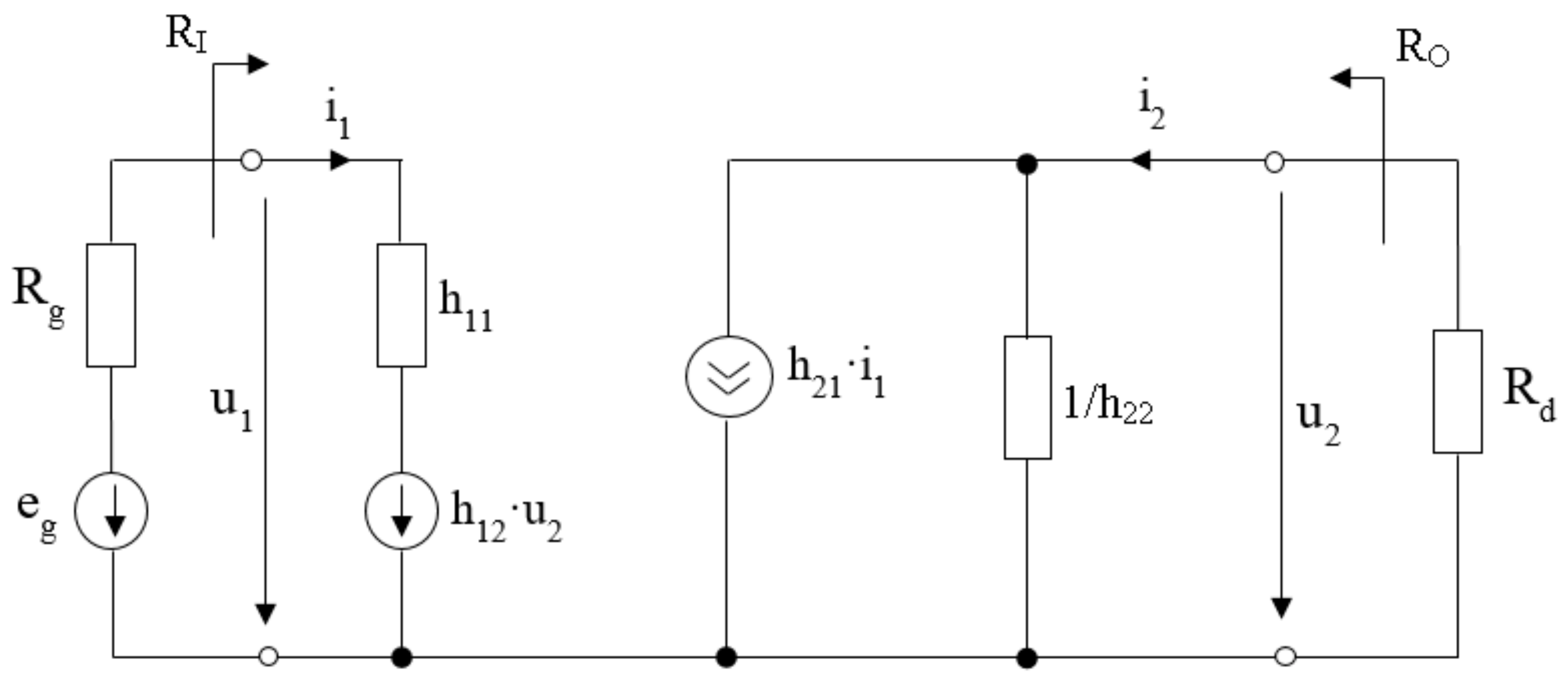
2. Determination of the Amplifying Parameters of the Stages in Various Connections

The stage amplifier parameters in common emitter, common collector and common base connections will be determined in this section.

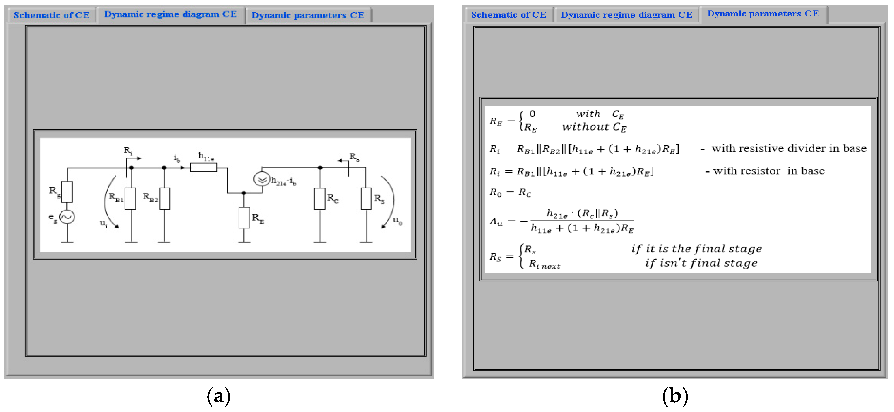
2.1. Common Emitter Connection

The main issue concerning common emitter connections will be presented in this paragraph [19,20,21,22,23]. Figure 2 shows the electronic scheme.
In this figure, capacitor C2, if connected in the scheme, is a by-pass capacitor of resistance RE. Because of the extremely low achievable impedance, the value of RE that is taken into consideration during the simulation process if capacitor C2 is utilized can be chosen from the application front panel. Alternatively, it can be left at 0. We assume that RE holds the value introduced from the application’s front panel if C2 is not used in the simulation. This fact leads one to believe that in simulations, RE has the value given by (2).
R E R E   o r   0 w i t h   C 2 R E w i t h o u t   C 2  
Two cases were studied in terms of equivalent resistance from the transistor’s base. In the first case, assume that both RB1 and RB2 are present in the scheme, implying that the transistor polarization is with a resistive divider in the base. In the second case, assume that only RB1 is present in the scheme, implying that the transistor is polarized with resistance in the base. Both scenarios are taken into account during the simulation process.
Figure 3 depicts the equivalent scheme in the dynamical regime for a common emitter connection.
For both cases presented above, the determination of the input resistance in dynamical regime, Ri, of the common emitter connection is based on relations (3) and (4).
R i = R B 1 R B 2 h 11 e + 1 + h 21 e R E   with   resistive   divider   in   base
R i = R B 1 h 11 e + 1 + h 21 e R E   with   resistance   in   base
Relation (5) made it possible to calculate the value of the output resistance, R0, in a dynamical regime.
R 0 = R C
Relation (6) can be used to calculate the value of voltage amplification, Au.
A u = h 21 e · R c R s h 11 e + 1 + h 21 e R E
In relation (6), the dynamical parameters of the used transistor are the input impedance, h11e, and amplification factor, h21e. The choice of load resistance Rs, as shown in relation (7), is dependent on whether the common emitter stage whose operation is being simulated is the final stage of a multiple stage amplifier or not.
R S R s                                               i f   i t   i s   t h e   f i n a l   s t a g e R I N                                                     i f   i s n t   f i n a l   s t a g e

2.2. Common Collector Connection

The main issue concerning common collector connections will be presented in this paragraph [15,16]. Figure 4 shows the electronic scheme.
In terms of equivalent resistance from the transistor’s base, the same two cases were studied as in the common emitter connection in terms of the presence of RB1 and RB2 resistance. Both scenarios are taken into account during the simulation process.
Figure 5 depicts the equivalent scheme in the dynamical regime for a common collector connection.
For both cases presented previously, the determination of the input resistance in dynamical regime, Ri, for a common collector connection is based on Relations (8) and (9).
R i = R B 1 R B 2 h 11 c + 1 + h 21 c · R E R S   with   resistive   divider   in   base
R i = R B 1 h 11 c + 1 + h 21 c R E   with   resistance   in   base
The determination of the output resistance in dynamical regime, R0, of the common collector connection is based on Relations (10) and (11) for both cases presented previously.
R 0 = R E h 11 c + R B 1 R B 2 R G / 1 + h 21 c   if   the   first   stage   is   with   resistive   divider   in   base
R 0 = R E h 11 c + R B 1 R G / 1 + h 21 c   if   the   first   stage   is   with   resistance   in   base
The choice of generator resistance RG, as shown in Relation (12), is determined by whether or not the common collector stage whose operation is being simulated is the first stage of a multiple stage amplifier.
R G R G                                         i f   i s   t h e   f i r s t   s t a g e R 0 ,   p r e v                                     i f   i s n t   f i r s t   s t a g e  
Relation (13) can be used to calculate the value of voltage amplification, Au.
A u = u 0 u i = ( R E R S ) ( 1 + h 21 c ) h 11 c + ( R E R S ) ( 1 + h 21 c )
The dynamical parameters of the used transistor in Relation (13) are the input impedance, h11c, and amplification factor, h21c. The choice of load resistance Rs, as shown in Relation (14), is determined by whether or not the common collector stage whose operation is being simulated is the final stage of a multiple stage amplifier.
R S R S                             i f   i s   t h e   f i n a l   s t a g e R I N                             i f   i s n t   f i n a l   s t a g e

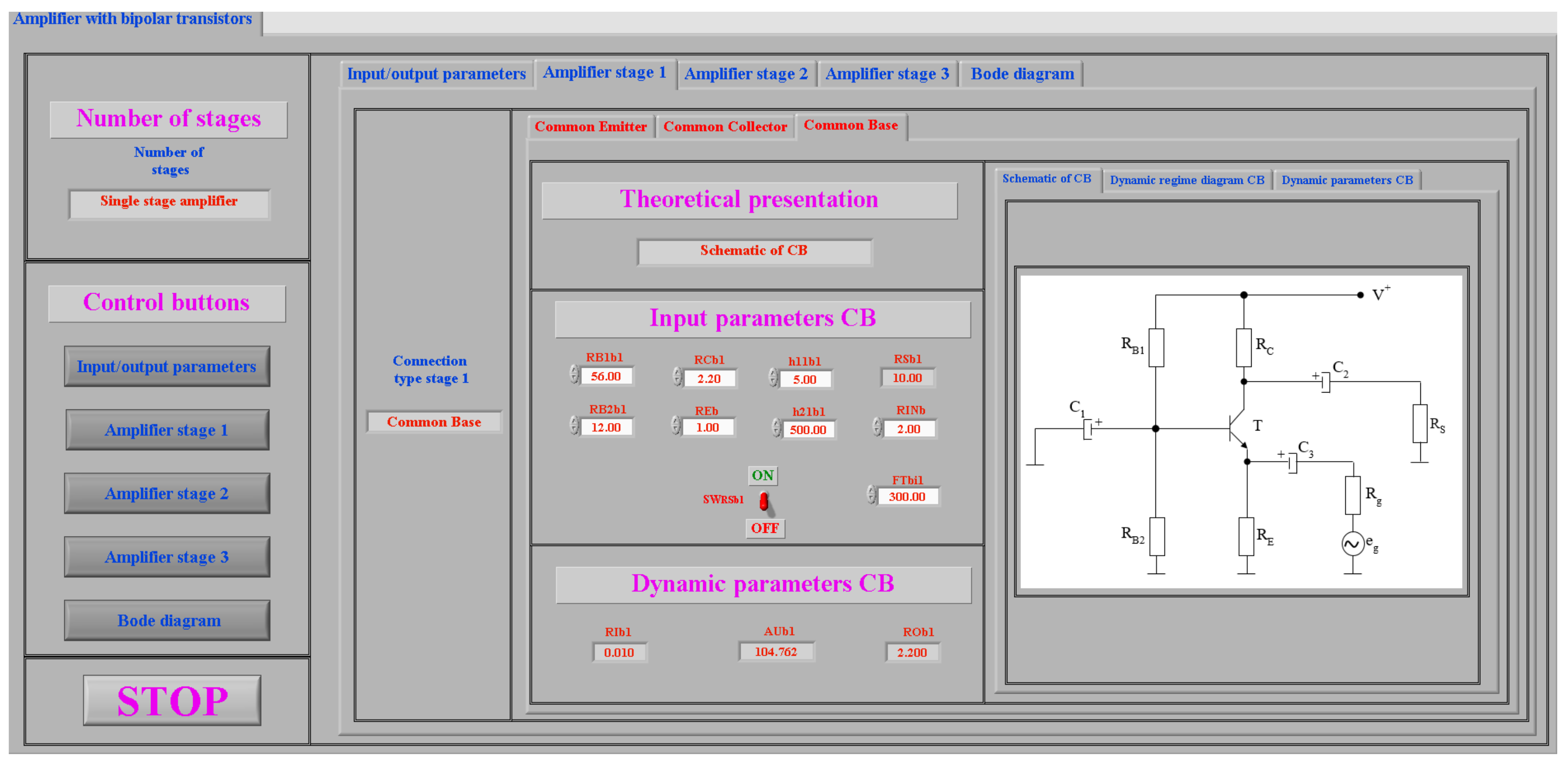
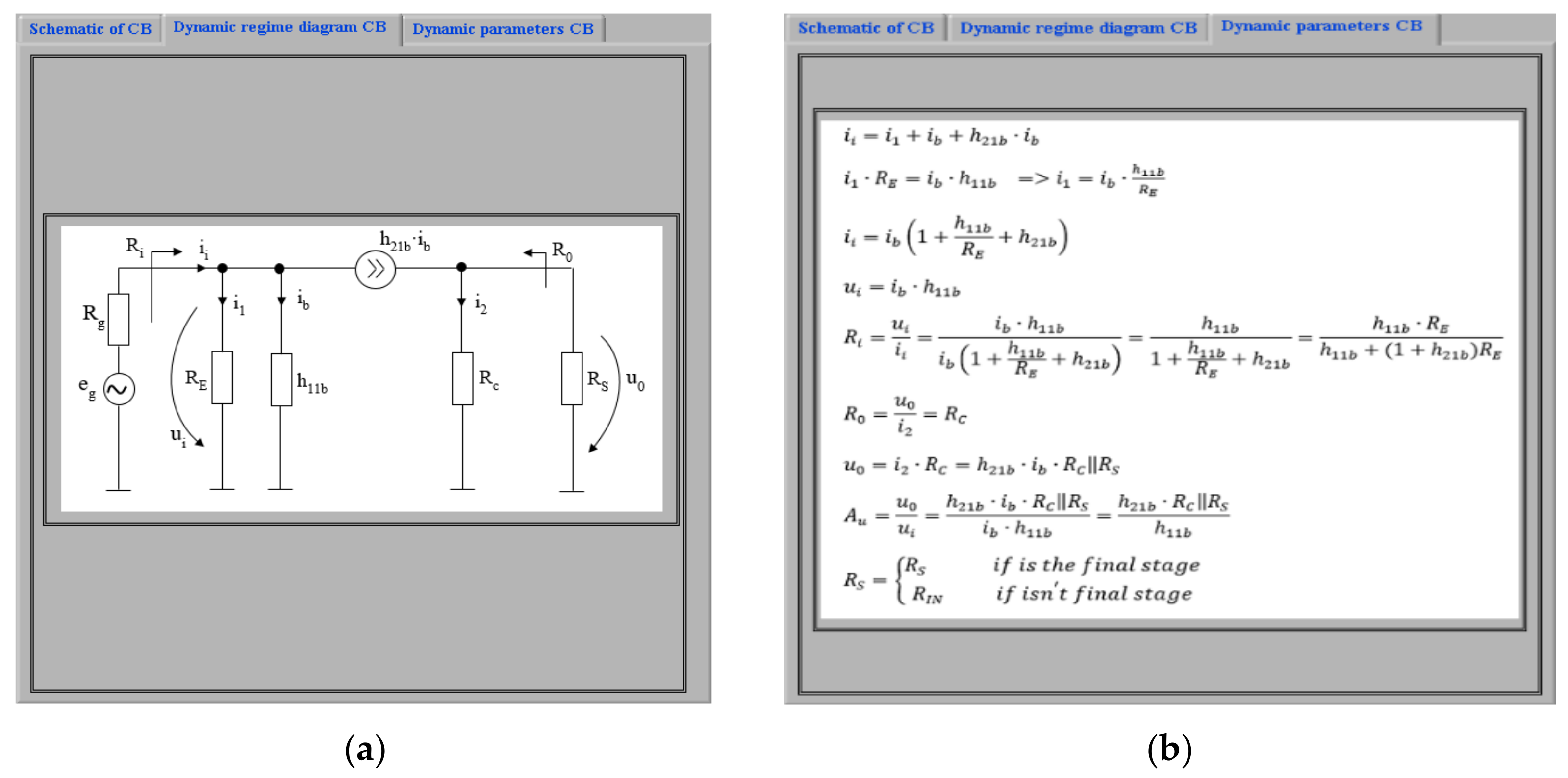
2.3. Common Base Connection

This paragraph will focus on the main issue of common base connections [15,21,22]. The electronic scheme is depicted in Figure 6.
Figure 7 depicts the dynamical equivalent scheme for a common base connection.
In Relation (15), the determination of the input resistance, Ri, in the dynamical regime in a common base connection is presented. The dynamical parameters of the used transistor in Relation (15) are the input impedance, h11b, and amplification factor, h21b.
R i = h 11 b · R E h 11 b + 1 + h 21 b R E
The value of the output resistance, R0, in dynamical regime in the common base connection can be computed from Relation (16).
R 0 = R C
Relation (17) can be used to calculate the value of voltage amplification, Au.
A u = h 21 b · R C R S h 11 b
The choice of load resistance Rs, as shown in Relation (18), is determined by whether or not the common base stage whose operation is being simulated is the final stage of a multiple stage amplifier.
R S = R S                             i f   i s   t h e   f i n a l   s t a g e R I N                         i f   i s n t   f i n a l   s t a g e

3. Presentation of LabVIEW-Implemented Applications

Figure 8 depicts the main application, which is a study of an amplifier using bipolar transistors [15]. The application is intended to use an amplifier with three stages, but this paper focuses on a situation with only one stage.
The number of stages can be selected in the left-upper part of Figure 8, which in this case contains only one stage. In the left section, there are also five control buttons that allow the selection of the amplifier’s input/output parameters, one of three amplifier stages, and finally a representation of the Bode diagram [24,25,26,27].

3.1. Input/Output Parameters

The “Input/output parameters” menu is depicted in Figure 8. This menu displays the equivalent scheme for the case where there is only one amplifier stage, as well as the relationships that allow voltage amplification to be calculated.
This menu allows you to select values for generator parameters, Rg and eg, load resistance, Rs, and coupling capacitors between the generator and the amplifier stage, CG, as well as the amplifier stage and the load, Cs.
In this figure, the parameters of the amplifier stage that is connected to the generator are also shown: input resistance, Ri1, output resistance, Ro1, and voltage amplification, Au1.

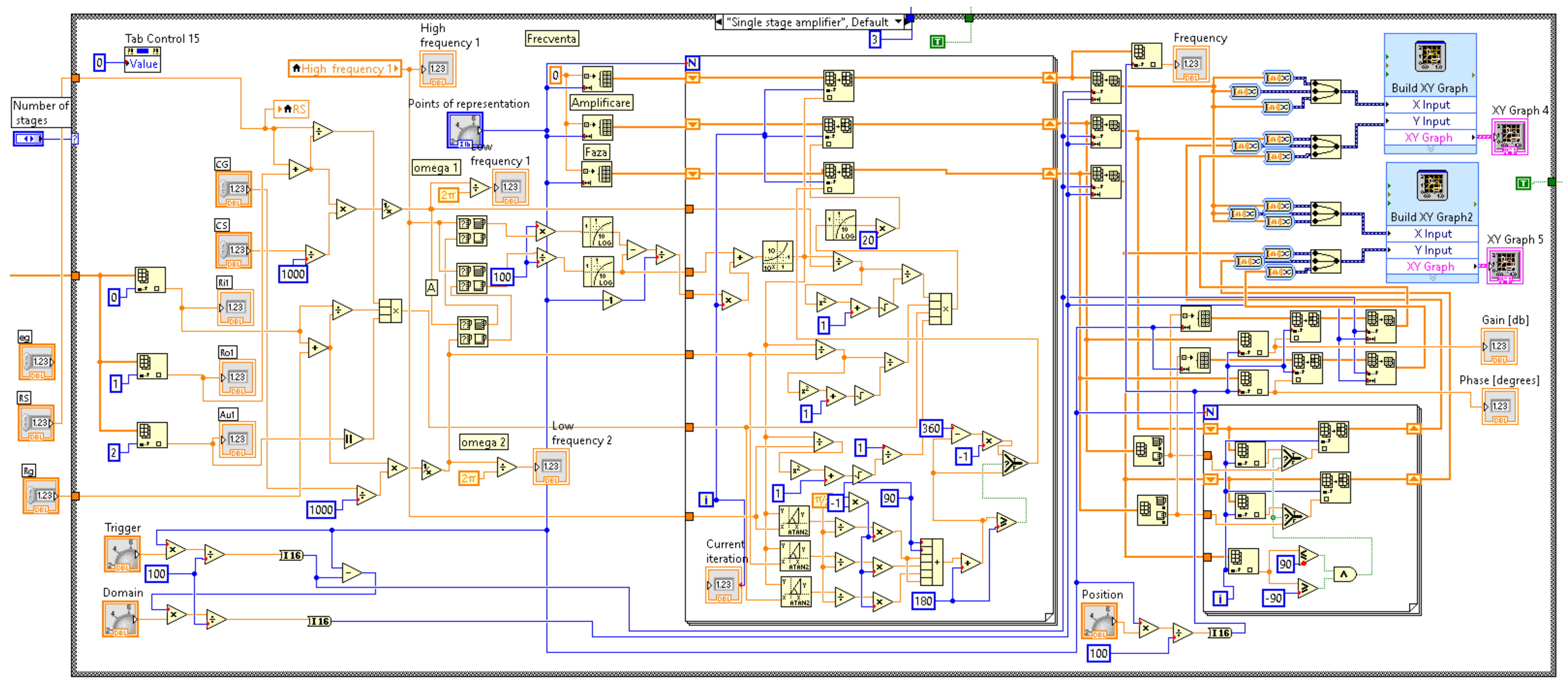
3.2. Implementation of the Presented Connections in LabVIEW

The implementation of all three connections will be presented in this section. For each connection, the front panel and the role of each element, as well as the programming panel, will be described [28,29,30].

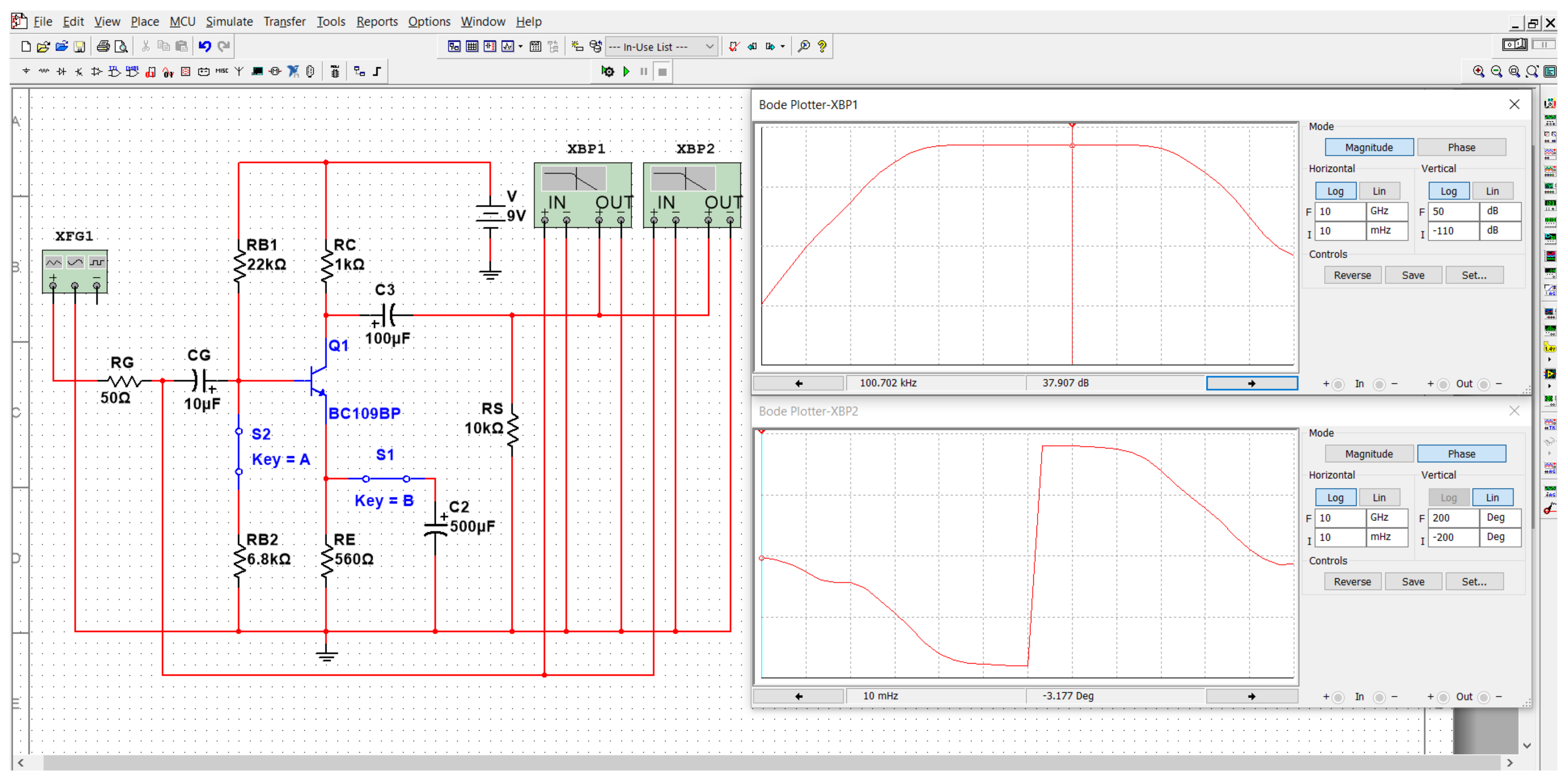
3.2.1. Implementation of an Amplifier Stage with a Common Emitter Connection

Figure 9 depicts the “Common emitter” menu [20,22]. This menu displays the amplifier stage’s scheme, as well as an option to view the dynamic regime diagram shown in Figure 10a, and the dynamic parameters for a common emitter connection shown in Figure 10b.
Users can select settings for common emitter stage input characteristics including base resistances RB1e1 and RB2e1, collector resistance RCe1, emitter resistance REe1, and dynamic regime parameters like input impedance, h11e1, and amplification factor h21e1. The high cutting frequency of the used transistor can be set from FTei1 using the data sheet transistor parameters.
The switch “SWRSe1” selects the value of RS from Relation (6) according to Relation (7), in the context of calculating stage voltage amplification.
The program allows the user to select the polarization mode of the transistor base with resistive divider or resistance in the base by using the switch “SWRB2e1”.
It is also possible to use the “SWCEe1” switch to connect/disconnect the resistor from the emitter and observe the effect on the amplifier parameters.
The dynamic parameters of the amplifier stage are computed based on the values of the input parameters: input resistance, RIe1, output resistance, ROe1, and voltage amplification, Aue1.
Figure 11a depicts the program’s implementation of parameters computed for a common emitter connection. This program employs the “EC1” subroutine, shown in Figure 11b, which is used to compute the output parameters.

3.2.2. Implementation of an Amplifier Stage with a Common Collector Connection

Figure 12 depicts the “Common collector” menu. This menu displays the amplifier stage’s scheme, as well as an option to view the dynamic regime diagram shown in Figure 13a, and the dynamic parameters for a common collector connection shown in Figure 13b.
Users can select settings for common collector stage input characteristics including base resistances RB1c1 and RB2c1, collector resistance RCc1, emitter resistance REc1, and dynamic regime parameters like input impedance, h11c1, and amplification factor h21c1. The high cutting frequency of the used transistor can be set from FTci1 using the data sheet transistor parameters.
The switch “SWRSc1” selects the value of RS from Relation (13) according to Relation (14), in the context of calculating stage voltage amplification.
The program allows the user to select the polarization mode of the transistor base with resistive divider or resistance in the base by using the switch “SWRB2c”.
To compute the value of Ro according to Relations (10) and (11), the value of RG can be selected as in (12) using the switch “SWRGc1”.
The dynamic parameters of the amplifier stage are computed based on the values of the input parameters: input resistance, RIc1, output resistance, ROc1, and voltage amplification, Auc1.
Figure 14a depicts the program’s implementation of parameters computed for a common collector connection. This program employs the “CC1” subroutine shown in Figure 14b, which is used to compute the output parameters.

3.2.3. Implementation of an Amplifier Stage with a Common Base Connection

Figure 15 depicts the “Common base” menu [19,22]. This menu displays the amplifier stage’s scheme, as well as an option to view the dynamic regime diagram shown in Figure 16a, and the dynamic parameters for a common base connection shown in Figure 16b.
Users can select settings for common emitter stage input characteristics including base resistances RB1b1 and RB2b1, collector resistance RCb1, emitter resistance REb1, and dynamic regime parameters like input impedance, h11b1, and amplification factor h21b1. The high cutting frequency of the used transistor can be set from FTbi1 using the data sheet transistor parameters.
The switch “SWRSb1” selects the value of RS from Relation (17) according to Relation (18), in the context of calculating stage voltage amplification.
The dynamic parameters of the amplifier stage are computed based on the values of the input parameters: input resistance, RIb1, output resistance, ROb1, and voltage amplification, Aub1.
Figure 17a depicts the program’s implementation of parameters computed for a common base connection. This program employs the “BC1” subroutine shown in Figure 17b, which is used to compute the output parameters.

3.3. Computing and Implementation of Bode Diagram

Figure 18 depicts the “Bode diagram” menu, which can be accessed via the control button “Bode diagram” [24,25,26,27]. The characteristics “Gain-Frequency” and “Phase-Frequency” are represented in a semi-logarithmic scale on the right side of this menu (linear scales for gain and phase and logarithmical scale for frequency). The gain and phase dependency for the frequency choice domain are represented by white lines. The red line represents the stability domain, where the phase is between −90° and 90°. A green line represents the position of a specified point on the graphs.
As seen from the gain-frequency characteristic, there are three characteristic points for a single stage of the amplifier. The first of them represents the high cutting frequency of the used transistor, which was set in the “Amplifier stage 1” menu in Figure 9. The next two characteristic points represent low cut frequencies, determined by CG, Ri1 and Rg for f1, and CS, Ro1 and RS for f2, calculated using Relations (19) and (20).
f 1 = 1 2 · π · C G · ( R i 1 + R g )
f 2 = 1 2 · π · C S · ( R o 1 + R S )
According to Relations (21) and (22), the frequency domain is chosen to range from a minimum frequency fmin to a maximum frequency fmax, providing the possibility of representing all three characteristic points.
f m i n = m i n f 1 ; f 2 10
f m a x = 10 · F T i 1
To obtain the graphs in Figure 18, the application computes the gain and phase values into a number of points that can be selected from the “Points of representation” knob, which is located in the [100;10,000] domain. The graphic resolution of the diagrams is defined by the number of points represented, N. Because the frequency has a logarithmic representation, the distance between two consecutive points is defined in Relation (23).
f = l o g f m a x l o g f m i n N 1
The starting point of the graphic representation can be set using the “Trigger” knob, which ranges from 0% to 100% of the full range of representation. The domain of representation can be selected from 0% to 100% of the total range of representation using the “Domain” knob.
The “Position” knob can be used to obtain information about a specific point. After selecting a specific point from the “Specific point” menu, information on frequency, gain, and phase can be obtained.
The program implementation of Bode diagrams for a single stage amplifier is shown in Figure 19.

4. Results of Simulation and Experimentation

This section contains simulation and experimentation results for an amplifier operating in the connections presented in Section 2: common emitter, common collector, and common base [31,32,33,34,35,36,37].
In order to validate the simulation results using the LabVIEW application, the specialized program Multisim was used, as well as experimental measurements using the Electronics Explorer Board. Bode characteristics can be determined using both Multisim and the Electronics Explorer Board. The same transistor was used in both simulations and experimental amplifiers.

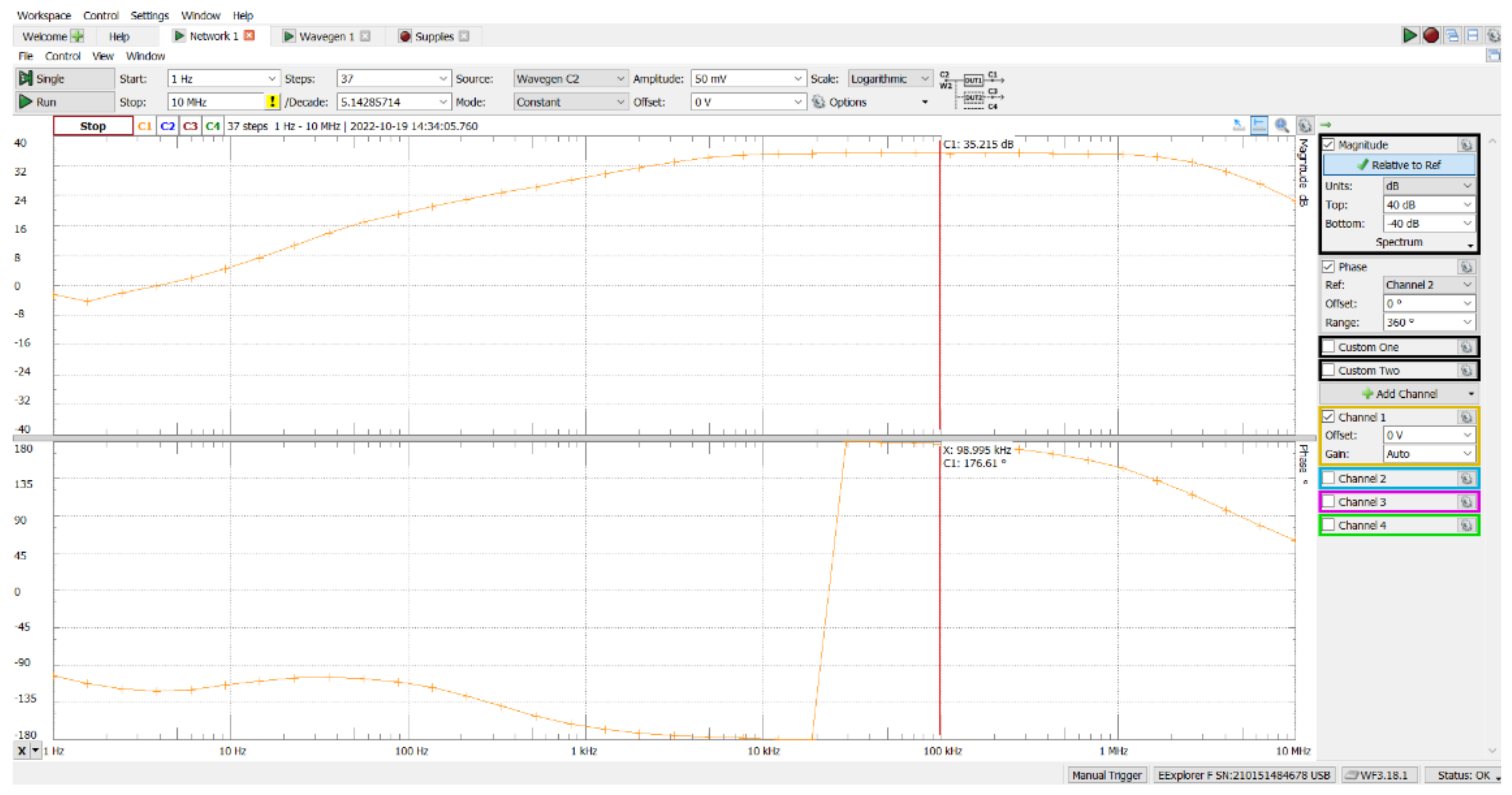
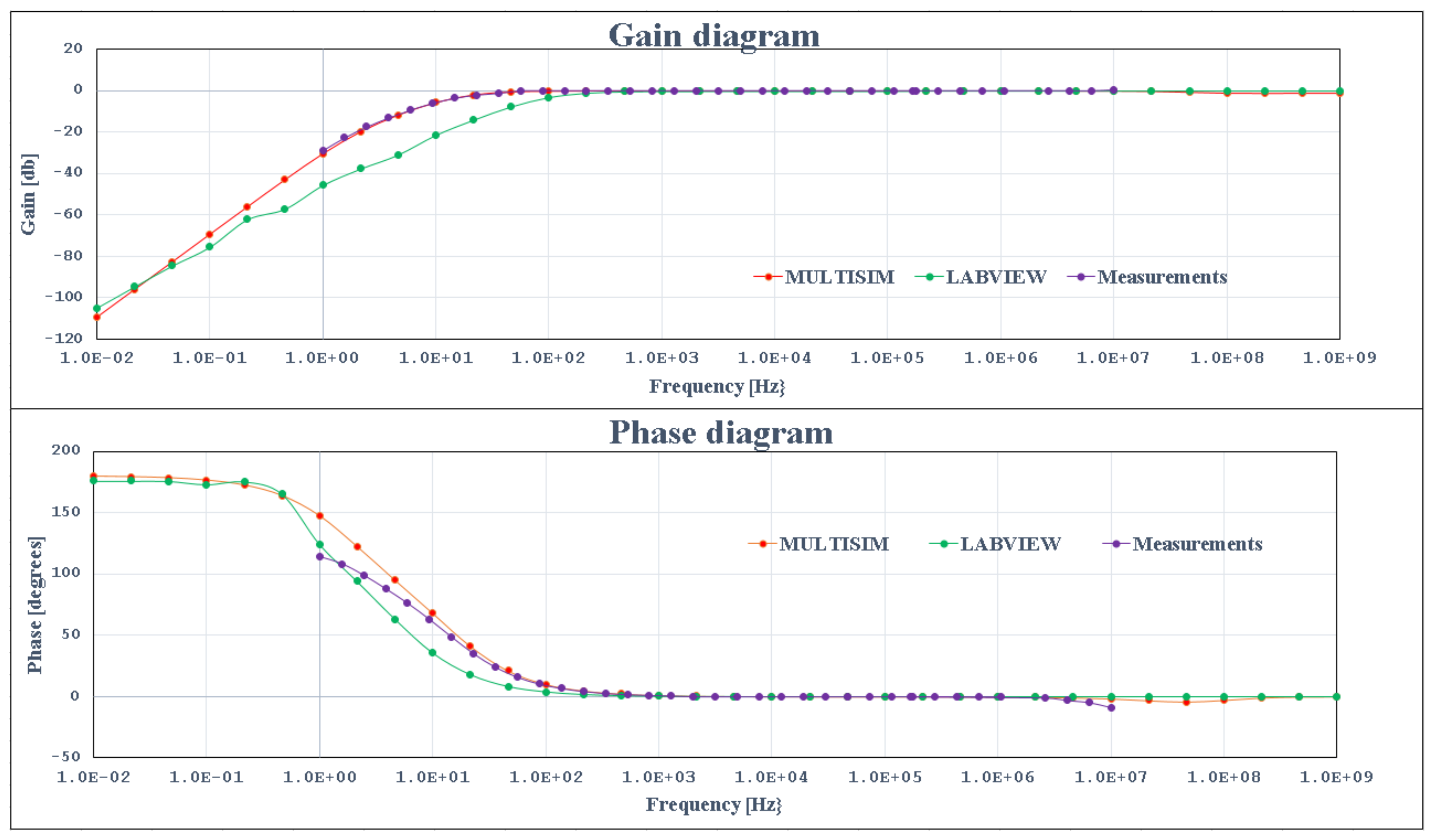
4.1. Simulation and Experimentation Results for Common Emitter Connection

The input parameter values for this connection were chosen in such a way that the Bode diagram presented two different low pulsations [15,16]. These values are: for generator parameters, Rg = 0.05 kΩ and eg = 10 mV; for load resistance, Rs = 10 kΩ; for coupling capacitors between generator and amplifier stage, CG = 10 µF; and for coupling capacitors between amplifier stage and load, Cs = 100 µF. As shown in Figure 9, Figure 12 and Figure 15, a BC 109 transistor with h11e = 5 k, h21e = 500, and fT = 300 MHz was used in both simulations and experimental measurements. These parameter values correspond to data from the Data Sheet.
The parameter values for the common emitter connection are presented in Figure 9.
As previously stated, the structure of an amplifier stage can be modified using the switches SWCEe1, SWRB2e1 and SWRSe1. Table 1 present the values of the output parameters RIe1, AUe1 and ROe1 for all situations in which SWCEe1, SWRB2e1 and SWRSe1 can be established.
Table 1 reveals some conclusions regarding the effect of the three switches on the values of the output parameters.
1. Connecting capacitor C2 from Figure 20 with the switch SWCEe1 in the ON state results in a significant increase in AUe1 and a decrease in RIe1.
2. Selecting the polarization mode of the transistor base with a resistive divider by connecting the switch SWRB2e1 in the ON state causes the input resistance RIe1 to decrease.
3. Switching SWRSe1 in the ON state is conducive to an increase in AUe1 of about 35%.
4. None of the three switches have any effect on the ROe1 value.
The effect of switch SWCEe1 can be seen in the Bode diagrams in Figure 20, Figure 21 and Figure 22 with SWCEe1 to ON, line 8 from Table 1. All of these figures were obtained through simulations with the presented application and allow for the low and high cut frequency to be determined. These frequencies were determined as the points where the gain was reduced by 3 decibels.
Figure 20. Bode diagram for line 8 from Table 1 with SWCEe1 to ON, for 10 kHz frequency.
Chips 03 00004 g020
Multisim, a specialized simulation program, was used to verify the LabVIEW simulation results. The simulation results obtained with Multisim are shown in Figure 23.
In order to validate the simulation results produced by LabVIEW and Multisim, experimental measurements were performed on a real circuit using an Electronic Explorer Board, which can also be used to determine the Bode characteristics. The Electronic Explorer Board has a frequency range of up to 10 MHz.
The measurement results obtained with the Electronic Explorer Board are presented in Figure 24.
A comparison between the simulations and the experimental results can be seen in Figure 25.
Analyzing the gain diagram reveals that the simulation and experimental results are very similar at medium and high frequencies. In terms of the phase diagram, both simulations and measurements achieve the same crossing from −180° to 180°, and the LabVIEW simulations and measured results are nearly identical at medium and high frequencies.
The effect of switch SWCEe1 can be seen in the Bode diagrams in Figure 26, Figure 27 and Figure 28 with SWCEe1 to OFF, line 4 from Table 1.
As in the previous situation when SWCEe1 was ON, a similar comparison between the simulations and experimental results can be made when SWCEe1 was OFF. The comparison results can be seen in Figure 29.
Analyzing the gain diagram reveals that the simulation results are very similar at medium and high frequencies. At medium frequencies both simulations and measurements are very close.
In terms of the phase diagram, both simulations and measurements achieve similar values when crossing from −180° to 180°, and the LabVIEW simulations and measurements are nearly identical at medium frequencies.

4.2. Simulation and Experimentation Results for Common Collector Connection

The input parameter values for this connection were chosen, like in the previous section, in such a way that the Bode diagram presented two different low pulsations [14,15,16]. These values are: for generator parameters, Rg = 0.05 kΩ and eg = 10 mV; for load resistance, Rs = 1 kΩ; for coupling capacitors between the generator and the amplifier stage, CG = 10 µF; and for coupling capacitors between amplifier stage and the load, Cs = 10 µF.
The parameter values for the common collector connection are presented in Figure 12.
As previously stated, the structure of an amplifier stage can be modified using the switches SWRGc1, SWRB2c1 and SWRSc1. Table 2 presents the values of the output parameters RIc1, AUc1 and ROc1 for all situations in which SWRGc1, SWRB2c1 and SWRSc1 can be established.
Table 2 reveals some conclusions regarding the effect of the three switches on the values of the output parameters.
1. Selecting the polarization mode of the transistor base with resistive divider by connecting switch SWRB2c1 in the ON state causes the input resistance RIc1 to decrease.
2. None of the three switches have any effect on the AUc1 value.
3. None of the three switches have any effect on the ROc1 value.
Figure 30 and Figure 31 show the Bode diagrams generated by simulations for the selected line from Table 2.
The simulation results for the common collector connection obtained with Multisim are shown in Figure 32.
Experimental measurements were performed on a real circuit using an Electronic Explorer Board, which can also be used to determine the Bode characteristics. The measurement results obtained with the Electronic Explorer Board are presented in Figure 33.
A comparison between the simulations and experimental results can be seen in Figure 34.
Analyzing the gain diagram reveals that the simulation and experimental results are similar at all frequencies.

4.3. Simulation and Experimentation Results for Common Base Connection

The input parameter values for this connection were chosen, like in the previous sections, in such a way that the Bode diagram presented two different low pulsations [14,15,16]. These values are: for generator parameters, Rg = 0.05 kΩ and eg = 10 mV; for load resistance, Rs = 10 kΩ; for coupling capacitors between the generator and the amplifier stage, CG = 1 µF; and for coupling capacitors between amplifier stage and the load, Cs = 100 µF.
The parameter values for the common base connection are presented in Figure 15.
As previously stated, the structure of an amplifier stage can be modified using the switch SWRSb1. Table 3 presents the values of the output parameters RIb1, AUb1 and ROb1 for the two situations in which SWRSb1 can be established.
Table 3 reveals some conclusions regarding the effect of the switch SWRSb1 on the values of the output parameters.
1. The state of the switch SWRSb1 has no effect on the input resistance RIb1 or the output resistance ROb1.
2. The ON state of switch SWRSb1 causes the AUb1 value to increase.
Figure 35, Figure 36 and Figure 37 show the Bode diagrams generated by simulations for the selected line from Table 3.
The simulation results obtained with Multisim are shown in Figure 38.
As with previous connections, to validate the simulation results produced by LabVIEW and Multisim, experimental measurements were performed on a real circuit using an Electronic Explorer Board.
The measurement results obtained with the Electronic Explorer Board are presented in Figure 39.
A comparison between the simulations and experimental results can be seen in Figure 40.
Analyzing the gain diagram reveals that the simulation and experimental results are similar at low and medium frequencies. At high frequencies the LabVIEW simulations and measurements are nearly identical.
In terms of the phase diagram, both simulations and measurements have the same behavior from 180° to −180°.

5. Conclusions

The investigation of the functionality of an amplifier with discrete components in various connections is a complex process due to the large number of circuit elements whose values influence the amplifier’s output parameters.
This paper describes a LabVIEW application that calculates the output parameters of a single-stage amplifier, such as input and output resistance, voltage amplification, and gain-frequency and phase-frequency Bode diagrams.
An amplifier stage can be studied in three different configurations: common emitter, common collector and common base. Different transistor polarisation possibilities can be selected for each connection. The application allows for the generation of various transistor polarization schemes by coupling some circuit elements with switches.
The amplifier’s stability zone, as well as the gain and phase of the amplifier for a given frequency value, can be determined using Bode diagrams.
A specified single-stage amplifier can be designed by changing both the configuration of the amplifier and the value of any circuit element.
Because the application allows the visualization of the electronic scheme of each connection, the mathematical relations for determining the output parameters, and the dynamical scheme, it can be used for educational purposes.
In order to validate simulation results from the LabVIEW application, the specialized program Multisim was used, as well as experimental measurements using the Electronics Explorer Board. Both Multisim and the Electronics Explorer Board can determine Bode characteristics. In both simulation and experimental amplifiers, the same schemes with the same transistor were used.
This paper demonstrated that the LabVIEW application can produce similar simulation results to Multisim or measured results using the Electronics Explorer Board. The application described in this article is an innovative type of tool that may be used as a learning tool because it performs circuit analysis in simulation software and experimental comparisons.
Figure 25, Figure 29 and Figure 34 show that the Multisim, LabVIEW, and measurement characteristics are not identical, which is due to the use of a simplified version of the quadrupole model used in simulations.
In the future, the authors intend to develop this application for two and three stages as a first step, followed by a study of different global reaction configurations as a second step.

Author Contributions

Conceptualization, C.C. and C.P.; methodology, M.P.; software C.P. and C.C.; validation, I.B. and S.M.; writing—original draft preparation, M.P. and S.M.; writing—review and editing, C.C., C.P. and M.P. All authors have read and agreed to the published version of the manuscript.

Funding

This research received no external funding.

Data Availability Statement

The raw data supporting the conclusions of this article will be made available by the authors on request.

Conflicts of Interest

The authors declare no conflict of interest.

Nomenclature

u1input quadrupole voltage
u2output quadrupole voltage
i1input quadrupole current
i2output quadrupole current
h11, h12, h21, h22quadrupole ”h” parameters
h11e, h12e, h21e, h22equadrupole ”h” parameters in common emitter connection
h11c, h12c, h21c, h22cquadrupole ”h” parameters in common collector connection
h11b, h12b, h21b, h22bquadrupole “h” parameters in common base connection
RI, ROinput and output resistance
RIe1, ROe1input and output resistance in common emitter connection
RIc1, ROc1input and output resistance in common collector connection
RIb1, ROb1input and output resistance in common base connection
Rggenerator resistance
Rddynamic resistance
eggenerator voltage
C1, C3coupling capacitors
C2decupling capacitors
RB1, RB2resistors connected on base
RB1e1, RB2e1resistors connected on base in common emitter connection
RB1c1, RB2c1resistors connected on base in common collector connection
RB1b1, RB2b1resistors connected on base in common base connection
RCresistors connected on collector
RCe1resistors connected on collector in common emitter connection
RCc1resistors connected on collector in common collector connection
RCb1resistors connected on collector in common base connection
REresistors connected on emitter
REe1resistors connected on emitter in common emitter connection
REc1resistors connected on emitter in common collector connection
REb1resistors connected on emitter in common base connection
Rsload resistor
Auvoltage amplification
Aue1voltage amplification in common emitter connection
Auc1voltage amplification in common collector connection
Aub1voltage amplification in common base connection
Ri,next, RINinput resistance of the next stage
Ro,prevoutput resistance of the previous stage
CGcoupling capacitors between the generator and the amplifier stage
Cscoupling capacitors between the amplifier stage and the load
Ri1input resistance
Ro1output resistance
SWRSe1, SWRB2e1, SWCEe1used switches in common emitter connection
SWRSc1, SWRB2c, SWRGc1used switches in common collector connection
SWRSb1used switch in common base connection
FTei1high cutting frequency transistor in common emitter connection
FTci1high cutting frequency transistor in common collector connection
FTbi1high cutting frequency transistor in common base connection
ω1, ω2low cut pulsations of the stage
ωmin, ωmaxminimum and maximum pulsation domain
Δωgraphic resolution of the pulsation axis
Nnumber of points represented

References

  1. Thomas, L. Floyd. In Electronic Devices, 5th ed.; Prentice Hall, Inc.: Hoboken, NJ, USA, 1999. [Google Scholar]
  2. Prasad, R. Analog and Digital Electronic Circuits; Springer: Berlin/Heidelberg, Germany, 2021. [Google Scholar]
  3. Singh, S.; Agrawal, S. Analog and Digital Electronics; Dreamtech Press: Wiley, India, 2021. [Google Scholar]
  4. Ciugudean, M. Devices and Electronical Circuits; Politechnics Publishing House: Timisoara, Romania, 1999. [Google Scholar]
  5. Pasca, S.; Tomescu, N.; Sztojanov, I. Analogical and Digital Electronics; Albastra Publishing House: Timisoara, Romania, 2011. [Google Scholar]
  6. Tian, T.; Na, A.; Zhao, X.M.; Zeng, L.N.; Tao, Y. System Design of AC Open-Loop Gain Measurement of Amplifier. Appl. Mech. Mater. 2013, 333, 475–476. [Google Scholar] [CrossRef]
  7. Radhakrishnan, R.K.; Sukumarapillai, K.; Hashemian, R. A nullor approach to the design of analog circuits for a desirable performance. Microelectron. J. 2018, 78, 54–62. [Google Scholar] [CrossRef]
  8. Jeschke, S.; Al-Zoubi, A.Y.; Pfeiffer, O.; Natho, N.; Nsour, J. Classroom-laboratory interaction in an electronic engineering course. In Proceedings of the International Conference on Innovations in Information Technology, Al Ain, United Arab Emirates, 16–18 December 2008; pp. 337–341. [Google Scholar]
  9. Qin, G.X.; Wang, G.G.; Mc Caughan, L.; Ma, Z.Q. Superiority of common-base to common-emitter heterojunction bipolar transistors. Appl. Phys. Lett. 2010, 97, 133506. [Google Scholar] [CrossRef]
  10. Rode, D.L. Output resistance of the common-emitter amplifier. IEEE Trans. Electron Devices 2005, 52, 2004–2008. [Google Scholar] [CrossRef]
  11. Okamoto, K.; Fujita, J.; Ishikawa, M.; Hattori, T. Original amplifier using only emitter and base of a Si bipolar transistor. In Proceedings of the 2014 IEEE International Meeting for Future of Electron Devices Kansai (IMFEDK), Kyoto, Japan, 19–20 June 2014; pp. 1–2. [Google Scholar]
  12. Jiang, N.Y.; Wang, G.G.; Ma, Z.Q. Analytical explanation of different RF characteristics exhibited with common-emitter and common-base bipolar transistors. In Proceedings of the 2004 Bipolar/BICMOS Circuits and Technology Meeting, Montreal, QC, Canada, 12–14 September 2004; pp. 112–115. [Google Scholar]
  13. Narasimhamurthy, K.C.; Bindhu, T.S.; Natraj, S.; Bharath, G.C.; Vismithata, S.A.; Shiva, A. Exploration of Common Emitter Amplifier in Remote Lab. Cyber-Phys. Syst. Digit. Twins 2020, 80, 623–633. [Google Scholar]
  14. Wakui, S. Relationship between parameter estimation method based on Bode diagram and co-quad diagram. Int. J. Jpn. Soc. Precis. Eng. 1997, 31, 227–231. [Google Scholar]
  15. Hahn, J.; Edison, T.; Edgar, T.F. A note on stability analysis using Bode plots. Chem. Eng. Educ. 2001, 35, 208–211. [Google Scholar]
  16. Fan, L.; Miao, Z. Admittance-Based Stability Analysis: Bode Plots, Nyquist Diagrams or Eigenvalue Analysis? IEEE Trans. Power Syst. 2020, 35, 3312–3315. [Google Scholar] [CrossRef]
  17. Li, L. Design of Electronic Circuit Virtual Measurement System based on LabVIEW. Agro Food Ind. Hi-Tech 2017, 28, 2036–2040. [Google Scholar]
  18. Huang, Z.; Wang, X. Development of virtual instrument motor experiment teaching system based on LabVIEW. J. Chem. Pharm. Res. 2014, 6, 1361–1368. [Google Scholar]
  19. Xu, K.; Tao, Y. Circuit Analysis Courseware Design Based on LabVIEW. In Proceedings of the International Conference on Education Technology, Management and Humanities Science (ETMHS 2015), Shaanxi, China, 21–22 March 2015; Volume 27, pp. 991–995. [Google Scholar]
  20. Peng, J.S. Integrated Simulation and Implementation Based on Multisim and LabVIEW. In Proceedings of the International Conference of China Communication (ICCC2010), Guangxi, China, 13–14 October 2010; pp. 295–297. [Google Scholar]
  21. Hui, I.S. Design of virtual circuit experiment based on the LabVIEW. In Proceedings of the International Power, Electronics and Materials Engineering Conference (IPEMEC 2015), Dalian, China, 16–17 May 2015; Volume 17, pp. 1118–1121. [Google Scholar]
  22. Li, Y.M.; Cai, B. Electronic Circuit Virtual Laboratory Based on LabVIEW and Multisim. In Proceedings of the 7th International Conference on Intelligent Computation Technology and Automation (ICICTA), Changsha, China, 25–26 October 2014; pp. 222–225. [Google Scholar]
  23. Dominguez, M.A.; Fernandez, J.A.; Carrillo, J.M.; de la Vega, P.T.M. Remote Interactive Experiments Using LabVIEW for Electronic Test Bench. In Proceedings of the Inted2011: 5th International Technology, Education and Development Conference, Valencia, Spain, 7–9 March 2011; pp. 749–754. [Google Scholar]
  24. Weihao, W.; Xiaoli, Q. Design of Electronic Virtual Experiment System Based on LabVIEW. IOP Conf. Ser. Mater. Sci. Eng. 2019, 490, 042024. [Google Scholar]
  25. Wang, W.T.; Zhao, J.C.; Gu, Z.F.; Liu, Z. Application of LabVIEW in teaching of circuit analysis. Exp. Sci. Technol. 2014, 12, 49–51. [Google Scholar]
  26. Piao, C.R. Design of the virtual instrument. J. Nav. Univ. Eng. 2006, 6, 82–85. [Google Scholar]
  27. Calatrava, A.A.; Marcos, R.M.; Damian, J.S.Q. A Pilot Experience with Software Programming Environments as a Service for Teaching Activities. Appl. Sci. 2021, 11, 341. [Google Scholar] [CrossRef]
  28. Richelli, A. Low-Voltage Integrated Circuits Design and Application. Electronics 2021, 10, 89. [Google Scholar] [CrossRef]
  29. Hasan, S.; Abbas, Z.K.; Parvez, M.A. Equivalent Circuit Modeling of a Dual-Gate Graphene FET. Electronics 2021, 10, 63. [Google Scholar] [CrossRef]
  30. Chung, D.; Woon, C.; Inyeob, J.; Joonhyeon, J. Design of Cut Off-Frequency Fixing Filters by Error Compensation of MAXFLAT FIR Filters. Electronics 2021, 10, 553. [Google Scholar] [CrossRef]
  31. Urdaneta, P.; María, C.; Amaia, M.Z.; Ibon, O.R. Recommendation Systems for Education: Systematic Review. Electronics 2021, 10, 1611. [Google Scholar] [CrossRef]
  32. Gürkan, S.; Karapınar, M.; Sorgunlu, H.; Öztürk, O.; Doğan, S. Development of a photovoltaic panel emulator and LabVIEW-based application platform. Comput. Appl. Eng. Educ. 2020, 28, 1291–1310. [Google Scholar] [CrossRef]
  33. Allawi, F.M.A. Educational interactive LabVIEW simulations of field hydraulic conductivity tests below water table. Comput. Appl. Eng. Educ. 2021, 29, 1480–1488. [Google Scholar] [CrossRef]
  34. Allawi, F.M.A. Educational interactive hydraulic and geometric design of a spillway using LabView and geometrical modeling. Comput. Appl. Eng. Educ. 2019, 27, 145–153. [Google Scholar] [CrossRef]
  35. Allawi, F.M.A. Educational interactive vector simulation of water table control designs using LabView. Comput. Appl. Eng. Educ. 2020, 28, 853–866. [Google Scholar] [CrossRef]
  36. Szávuly, M.I.; Tóos, Á.; Barabás, R.; Szilágyi, B. From modeling to virtual laboratory development of a continuous binary distillation column for engineering education using MATLAB and LabVIEW. Comput. Appl. Eng. Educ. 2019, 27, 1019–1029. [Google Scholar] [CrossRef]
  37. RiveraOrtega, U. A simple LabVIEW-MATLAB implementation to observe the wavelength tunability of a laser diode with a diffraction grating. Comput. Appl. Eng. Educ. 2016, 24, 365–370. [Google Scholar] [CrossRef]
Figure 1. An equivalent circuit of an amplifier stage using the quadrupole “h” parameters.
Chips 03 00004 g001
Figure 2. Electronic scheme for common emitter connection.
Chips 03 00004 g002
Figure 3. The equivalent scheme in dynamical regime for a common emitter connection.
Chips 03 00004 g003
Figure 4. Electronic scheme for a common collector connection.
Chips 03 00004 g004
Figure 5. The equivalent scheme in dynamical regime for a common collector connection.
Chips 03 00004 g005
Figure 6. Electronic scheme for common base connection.
Chips 03 00004 g006
Figure 7. The equivalent scheme in dynamical regime for a common base connection.
Chips 03 00004 g007
Figure 8. Front panel for input/output parameters.
Chips 03 00004 g008
Figure 9. Front panel for common emitter stage parameters.
Chips 03 00004 g009
Figure 10. (a) Dynamic regime diagram CE, (b) Dynamic parameters CE.
Chips 03 00004 g010
Figure 11. (a) Program implementation of computed parameters, (b) Subroutine EC1.
Chips 03 00004 g011
Figure 12. Front panel for common collector stage parameters.
Chips 03 00004 g012
Figure 13. (a) Dynamic regime diagram CC, (b) Dynamic parameters CC.
Chips 03 00004 g013
Figure 14. (a) Program implementation of computed parameters, (b) Subroutine CC1.
Chips 03 00004 g014
Figure 15. Front panel for common base stage parameters.
Chips 03 00004 g015
Figure 16. (a) Dynamic regime diagram CB, (b) Dynamic parameters CB.
Chips 03 00004 g016
Figure 17. (a) Program implementation of computed parameters, (b) Subroutine BC1.
Chips 03 00004 g017
Figure 18. Bode diagram menu.
Chips 03 00004 g018
Figure 19. Program implementation of Bode diagram menu.
Chips 03 00004 g019
Figure 21. Bode diagram for line 8 from Table 1 with SWCEe1 to ON, for low cut frequency of 38.66 Hz.
Chips 03 00004 g021
Figure 22. Bode diagram for line 8 from Table 1 with SWCEe1 to ON, for high cut frequency of 3.29 MHz.
Chips 03 00004 g022
Figure 23. Simulation results for common emitter connection with SWCEe1 to ON, using Multisim.
Chips 03 00004 g023
Figure 24. Measurement results for common emitter connection with SWCEe1 to ON, using Electronic Explorer Board.
Chips 03 00004 g024
Figure 25. Simulations and experimental results for common emitter connection with SWCEe1 to ON.
Chips 03 00004 g025
Figure 26. Bode diagram for line 4 from Table 1 with SWCEe1 to OFF, for 10 kHz frequency.
Chips 03 00004 g026
Figure 27. Bode diagram for line 4 from Table 1 with SWCEe1 to OFF, for low cut frequency of 19.5 Hz.
Chips 03 00004 g027
Figure 28. Bode diagram for line 4 from Table 1 with SWCEe1 to OFF, for high cut frequency of 188.7 MHz.
Chips 03 00004 g028
Figure 29. Simulations and experimental results for common emitter connection with SWCEe1 to OFF.
Chips 03 00004 g029
Figure 30. Bode diagram for line 5 from Table 2, for 10 kHz frequency.
Chips 03 00004 g030
Figure 31. Bode diagram for line 5 from Table 2, for low cut pulsations of 98.85 Hz.
Chips 03 00004 g031
Figure 32. Simulation results for common collector connection, using Multisim.
Chips 03 00004 g032
Figure 33. Measurement results for common collector connection, using Electronic Explorer Board.
Chips 03 00004 g033
Figure 34. Simulations and experimental results for common collector connection.
Chips 03 00004 g034
Figure 35. Bode diagram for line 1 from Table 3, for 10 kHz frequency.
Chips 03 00004 g035
Figure 36. Bode diagram for line 1 from Table 3, for low cut pulsations of 447.9 Hz.
Chips 03 00004 g036
Figure 37. Bode diagram for line 1 from Table 3, for high cut pulsations of 2.86 MHz.
Chips 03 00004 g037
Figure 38. Simulation results for common base connection, using Multisim.
Chips 03 00004 g038
Figure 39. Measurement results for common base connection, using Electronic Explorer Board.
Chips 03 00004 g039
Figure 40. Simulations and experimental results for common base connection.
Chips 03 00004 g040
Table 1. The values of the output parameters.
SWRB2e1SWRSe1RIe1 [kΩ]AUe1ROe1 [kΩ]
OFFOFFOFF20.426−1.1671.000
OFFOFFON20.426−1.5921.000
OFFONOFF5.102−1.1671.000
OFFONON5.102−1.5921.000
ONOFFOFF4.074−66.6671.000
ONOFFON4.074−90.9091.000
ONONOFF2.548−66.6671.000
ONONON2.548−90.9091.000
Table 2. The values of the output parameters.
SWRGc1SWRB2c1SWRSc1RIc1 [kΩ]AUc1ROc1 [kΩ]
OFFOFFOFF17.0920.9850.013
OFFOFFON16.8150.9800.013
OFFONOFF8.7670.9850.013
OFFONON8.6940.9800.013
ONOFFOFF17.0920.9850.013
ONOFFON16.8150.9800.013
ONONOFF8.7670.9850.013
ONONON8.6940.9800.013
Table 3. The values of the output parameters.
SWRSb1RIb1 [kΩ]AUb1ROb1 [kΩ]
OFF0.013104.7622.200
ON0.013180.3282.200
Disclaimer/Publisher’s Note: The statements, opinions and data contained in all publications are solely those of the individual author(s) and contributor(s) and not of MDPI and/or the editor(s). MDPI and/or the editor(s) disclaim responsibility for any injury to people or property resulting from any ideas, methods, instructions or products referred to in the content.

