
Silicon Radiation Detector Technologies: From Planar to 3D

1
Department of Industrial Engineering, University of Trento, Via Sommarive 9, 38123 Trento, Italy
2
Trento Institute for Fundamental Physics and Applications (TIFPA-INFN), Via Sommarive 14, 38123 Trento, Italy
*
Author to whom correspondence should be addressed.
Chips 2023, 2(2), 83-101; https://doi.org/10.3390/chips2020006
Submission received: 25 February 2023
/
Revised: 7 April 2023
/
Accepted: 10 April 2023
/
Published: 13 April 2023
(This article belongs to the Special Issue Smart IC Design and Sensing Technologies)
Abstract
:Silicon radiation detectors, a special type of microelectronic sensor which plays a crucial role in many applications, are reviewed in this paper, focusing on fabrication aspects. After addressing the basic concepts and the main requirements, the evolution of detector technologies is discussed, which has been mainly driven by the ever-increasing demands for frontier scientific experiments.
1. Introduction
Radiation detectors are nowadays pervasive in several applications, from industry to medicine, from cultural heritage to environmental monitoring, homeland security and safety (e.g., in nuclear power plants), to cite but a few, as well as in many fields of fundamental and applied research, including high energy physics (HEP), photon science and astronomy.
Starting from the earliest devices, the detection of radiation has been based on different physical mechanisms, such as thermal transduction, gas ionization, scintillation, etc. [1]. As with most other sensor technologies, semiconductors also play a special role in radiation detection for two main reasons: (i) they can directly convert radiation into an electrical signal, ready to be processed by an electronic circuit, and (ii) they are fabricated by exploiting integrated circuit technologies, leading to several advantages, such as small size, low cost as well as improved performance and reliability [2]. Its physical properties (e.g., atomic number, density, ionization energy, bandgap, etc.) make silicon particularly suited for the detection of soft X-rays and charged particles, whereas it is not efficient for hard X-rays/γ-rays and for neutrons (for the detection of which silicon should be coupled with suitable converting materials) [1]. However, silicon is the most widely used semiconductor for detector applications, thanks to the unparalleled advantages of its fabrication technology.
Although silicon detectors are relatively simple devices, they require custom fabrication technologies to optimize their electrical and functional characteristics. Only recently, following the significant progress in CMOS image sensors, pixel detectors made with CMOS technologies (the so-called Monolithic Active Pixels) have proved to yield satisfactory performance [3]. In the future, there will likely be a greater utilization of CMOS pixels, particularly in X-ray imaging and charged particle tracking. However, custom-made detectors are still expected to remain the primary choice for most applications. The market for silicon detectors is considered a specialized one within the field of microelectronics, with only one major industrial manufacturer, Hamamatsu Photonics K.K. of Japan, operating in this area. The majority of the processing facilities are owned by small to medium-sized enterprises (SMEs) and research centers, primarily located in Europe.
In this paper, we will review silicon radiation detector technologies. Section 2 will recall the devices’ basic principles and the main requirements. Section 3 will be devoted to technological aspects, from starting materials to processing issues relevant to planar detectors (including detectors with integrated electronics and emerging detectors with intrinsic amplification) and 3D detectors.
2. Basic Principles and Requirements
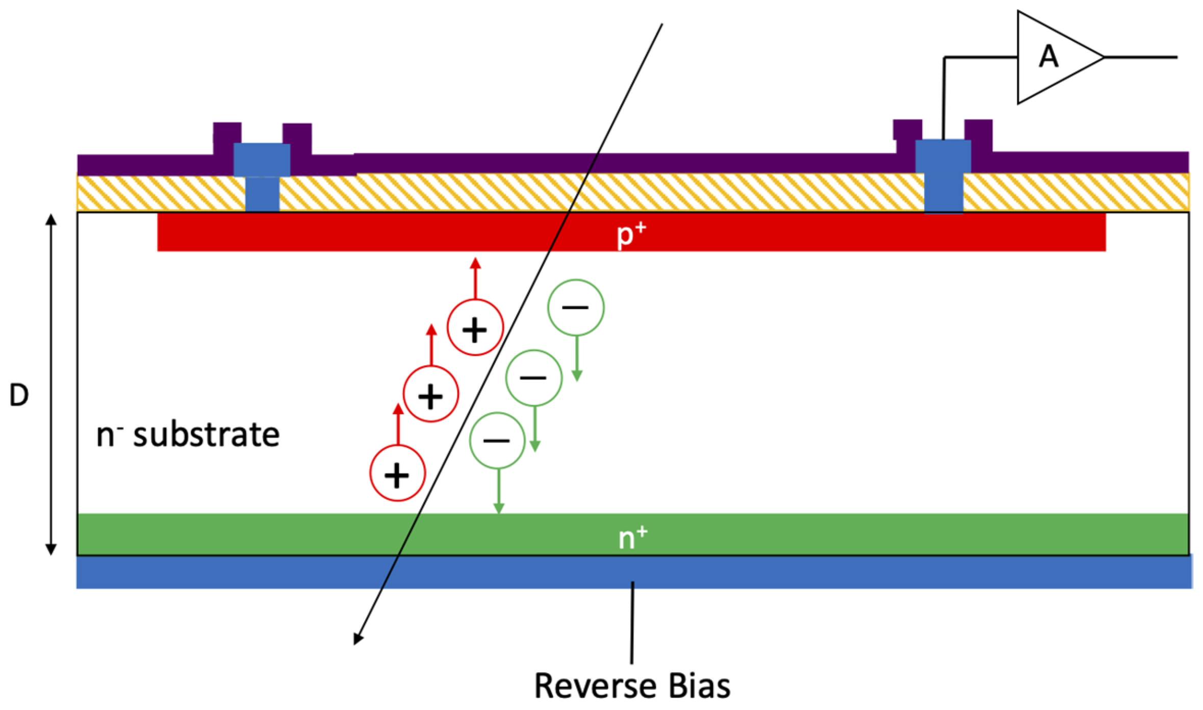
The most important types of silicon detectors are based on reverse biased p-n junctions [2]. The operation principle is sketched in Figure 1. When traversing through a silicon detector, an impinging radiation creates electron–hole pairs along its path. In the presence of an electric field, these charge carriers are separated and start drifting toward the electrodes, thus inducing a current signal [4], which is fed to an external amplifier.
Silicon detectors are typically operated in full depletion conditions in order to obtain optimal efficiency, high signal-to-noise ratio and short time response. With reference to the basic theory of an abrupt p+-n junction, the depletion width () can be expressed as in Equation (1):
where is the permittivity of silicon, the built-in voltage, the applied reverse bias voltage, the elementary charge and the substrate doping concentration. Thus, the full depletion voltage can be calculated as in Equation (2):
where is substrate thickness and assuming to be negligible. Depending on the applications, can vary from just a few μm (e.g., for dosimetry) up to ~1 mm (e.g., for X-ray imaging), with the most typical values being of a few hundreds of micrometers. In order to limit the value of full depletion voltage, so as to avoid junction breakdown and reduce power dissipation, the substrate doping concentration should be very low (~1012/cm3).
Despite their simple structure, silicon detectors have some special requirements:
- Very low leakage currents. Besides affecting power dissipation, the leakage current plays a critical role in the detector noise, so it should be minimized. A value < 1 nA/cm2 is normally assumed as a target. The leakage current is mainly caused by thermal generation in the depleted bulk, so the carrier lifetimes should be high enough, calling for high-purity material and ultra-clean processing, as well as for an optimized layout, often including guard rings [5].
- Large breakdown voltage. In certain cases, detectors require extremely high voltage to operate effectively. This may be due to factors such as thick substrates, the necessity to achieve high electric fields for velocity saturation, or radiation damage. Specifications often require the breakdown voltage to exceed several hundreds of volts. The use of guard rings is also useful in this respect [6].
- Radiation hardness. This is especially the case of detectors used in HEP experiments at particle colliders, where the fluences can be as large as ~1016 1-MeV equivalent neutrons per square cm (neq/cm2). Displacement damage to the silicon lattice is here the main issue, with three main consequences [7]: (i) increase in leakage current (linear with fluence); (ii) change in the effective space-charge concentration, leading to an increase in depletion voltage at large fluences; (iii) charge carrier trapping, which represents the factor ultimately limiting the detector performance at fluences beyond~1015 neq/cm2. In addition, ionization damage effects [8] are caused by charged particles but also by high-energy photons (X- and γ-rays), with total ionizing doses that can largely exceed 1 Grad in applications at particle colliders and at Free Electron Laser facilities [9]. The consequences are the build-up of positive charge in the oxides and of interface states, which affect the isolation between n+ regions, the parasitic capacitance between adjacent regions (with impact on noise), the electric fields at the surface (with impact on breakdown voltage) and surface generation/recombination (with impact on leakage current and charge collection in case radiation is absorbed near the surface).
- In silicon detectors, the minimum feature sizes are not too small (~micrometers). Proximity lithography is mainly used, sometimes with double-side alignment. The overall device dimensions can be very large (up to tens of square centimeters) and the specifications often require the total number of defects to be very small, so that yield is certainly a major concern in detector fabrication.
3. Fabrication Technologies
3.1. Starting Material
Most radiation detectors are fabricated on “detector-grade” (high-resistivity, high-purity) silicon wafers, which are usually obtained by the floating zone (FZ) refinement of hyper-pure silicon rods [10]. In this technique, induction heating by a RF coil allows for a free suspension of the silicon melt without any contact with foreign material, so that contaminations are almost absent. Ingots are available with a diameter of up to 8 inches (200 mm), limited by the instability of the melted zone at larger diameters. High-resistivity values ranging from ~1 kΩ cm to ~30 kΩ cm can be obtained, corresponding to dopant concentrations in the range of 1011–1012 cm−3, with non-uniformities lower than 30%. The concentration of normally undesired impurities, such as oxygen and carbon, is typically lower than 1016 cm−3, whereas minority carrier lifetime values are typically several milliseconds [11].
Historically speaking, most detectors were fabricated on n-type silicon substrates until the early 2000s, whereas recently p-type material has become more popular. Besides the availability of the raw material, this was motivated mainly by some advantages in those applications involving significant effects from bulk radiation damage, as will be explained in Section 3.2.1.
Besides FZ wafers, other types of silicon substrates are sometimes used:
- Neutron-transmutation-doped (NTD) substrates [11] are obtained from the irradiation of high-purity p-type silicon with fast neutrons, yielding n-type material with high-resistivity up to 5 kΩ cm. NTD wafers feature the lowest non-uniformities in the doping concentration, down to 5%, which is important for some types of detectors (e.g., drift detectors).
- Czochralski (CZ), Magnetic Czochralski (MCZ) and epitaxial wafers have also been recently used for the fabrication of silicon detectors in HEP applications. In fact, these types of substrates have a high concentration of oxygen, in the range of 1017–1018 cm−3, which was found to be beneficial in terms of radiation hardness of the detectors, since it lowers the increase in the effective space charge concentration at high radiation fluences, thus reducing the depletion voltage [12].
3.2. Planar Technology
3.2.1. Common Detector Types
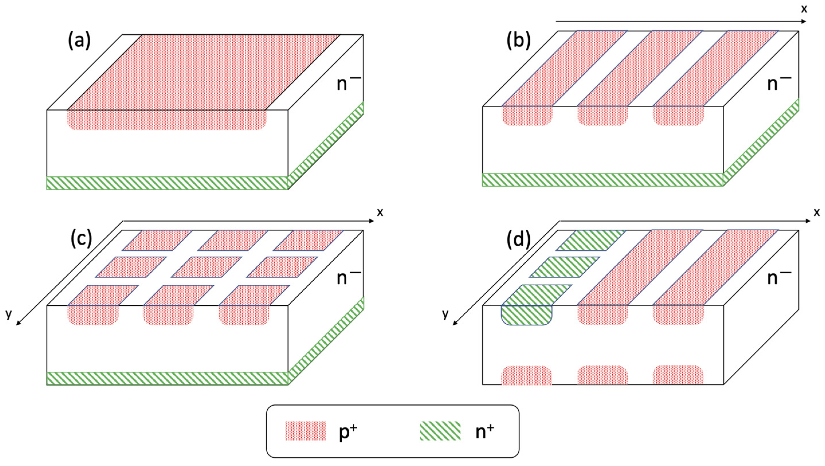
Silicon detectors are mainly used for spectroscopy and imaging/tracking applications. The most common types of planar detectors are sketched in Figure 2; they include pad detectors, microstrip detectors, pixel detectors and drift detectors [2].
Pad detectors (Figure 2a) are simple p-n junction diodes, with typical sizes ranging from a few hundred micrometers to centimeters. Since the substrate is high-resistivity (i.e., almost intrinsic), these detectors are often referred to as P-I-N diodes. They are nearly ideal detectors for α-particles and other light ions, providing very good energy resolution and stability, reduced drift, excellent timing performances, thin entrance window and simplicity of operation [1].
Position sensitivity is obtained by segmenting at least one of the electrodes, e.g., in the form of either parallel microstrips (Figure 2b) or of pixels (Figure 2c) [13]. Microstrips have a width of a few tens of micrometers (and a comparably large gap) and a length up to a few centimeters [14]. In principle, each microstrip should be connected to an electronic readout channel at its end. The X position of the passage of an ionizing particle is given by the location of the strip(s) showing a signal: in case of binary readout (i.e., assuming the center of a hit strip as the measured coordinate), the resolution is , where p is the pitch, and it typically ranges from ~20 to 100s of micrometers. Better values, down to ~1 μm, could be achieved for small-pitch microstrips in case of analogue readout with interpolation algorithms based on charge measurement at adjacent strips [15]. For X-Y position measurements, microstrip detectors can be mounted back-to-back with orthogonal orientation. In more advanced designs, the wafer back-side (ohmic side) is also segmented in microstrips [16], at the expense of a significant complication in the technology, as discussed later in this paper. With respect to the strips on the junction side, those on the ohmic side can be either orthogonal or just rotated by a small angle, in the so-called stereo configuration. Microstrip detectors can be made with a very large active area (tens of cm2, see, e.g., Figure 3), while preserving a very good position resolution, so that they are often used for tracking in high-energy physics and nuclear physics [17,18].
Pixel detectors are two-dimensional arrays of PIN diodes (Figure 2c), where the size of each diode is typically from 10s to 100s of micrometers. Depending on the specific configuration, pixel detectors can be fabricated with either a single-sided process (p-on-n, n-on-p) or a double-sided one (mainly n-on-n, whereas p-on-p is seldom used). P-on-n pixels were the first to be introduced and are the simplest to fabricate, since they require a single-sided technology without need for surface isolation layers between p+ pixels on the segmented side. As an example, they were used in the ALICE experiment at the LHC, where radiation damage issues are limited [19]. However, p-on-n pixels are not favored for applications in high radiation environments, because n-type substrates undergo type-inversion of the effective doping concentration after fluences of the order of ~1013 (neq/cm2) [20]. After type-inversion, the electric field distribution is less convenient, with the main junction moving to the n+ backside, where the weighting field is very small, eventually leading to a degradation in the charge collection efficiency after large fluences [21]. Therefore, other pixel options have later been developed which feature n-side signal readout (n-on-n and n-on-p). These devices exploit the higher mobility (hence longer drift length) of electrons with respect to holes, which results in faster signals and higher radiation tolerance, as well as allows for operation with partially depleted substrates [22]. N-on-n pixels, developed in the late 90s, were chosen for the ATLAS and CMS pixels at the LHC [23,24]. The n+ pixels on the frontside are kept at virtual ground by the readout amplifier, whereas the p+ back side must also be patterned to introduce a sufficiently wide gap (including floating guard rings) between the main junction where the reverse bias voltage is applied and the cut edge of the sensor, which must be at ground level. Thus, a double-sided technology is required, with an impact on costs. N-on-p sensors represent a convenient and less expensive alternative, since they can be fabricated with a simpler, single-sided technology (only the pixel side is patterned), while yielding the same performance after large radiation fluences, also avoiding type inversion.
The major drawback of pixel detectors is the need to connect each pixel to a read-out electronic channel, which requires complicated and expensive vertical interconnect techniques, such as bump bonding and flip-chipping [25]. Pixel detectors are mainly used as vertex detectors in high energy physics experiments, but they are also very interesting for imaging applications [26].
Silicon drift detectors (SDDs) were first proposed by E. Gatti and P. Rehak in 1984 [27,28]. They are made on high-resistivity n-type silicon wafers with rectifying p+-n junctions implanted on both wafer sides (see Figure 2d) and all reverse biased to obtain full depletion. An electrostatic potential parallel to the surface is then superimposed to the depleting vertical potential by means of resistive voltage dividers. When radiation is absorbed in the detector, creating e-h pairs, holes are swept away by the p+ electrodes close to the point of interaction, whereas electrons drift along the bottom of the potential valley toward a small collecting anode located aside, inducing a signal when they arrive close to it. Linear SDDs are mainly used for charged particle tracking and have two-dimensional position resolution: since the drift velocity is known, one coordinate of the interaction point (X in Figure 2) can be reconstructed from the measurement of the drift time of the electrons using either an external trigger or a “self-trigger” as obtained by reading the signal from the p+ strips, whereas the resolution on the second dimension (Y in Figure 2) is obtained by segmenting the anode in several adjacent pixel anodes [29]. On the contrary, SDDs used for X-ray spectroscopy have an individual anode at the center of an enclosed (typically circular) geometry. In this configuration, a uniform p+-n junction is used rather than circular rings on the detector side opposite to the anode, where a thin entrance window (especially important for soft X-rays) is often required [30,31]. The main advantage of SDDs is that the anode capacitance is much lower than that of standard junction detectors of the same overall area, thus allowing for very low noise and much better energy resolution at lower shaping times (thus enabling higher operation rates) [32]. One disadvantage of silicon drift detectors is the rather complicated bias electronic circuitry necessary to distribute the longitudinal potential among all the p+ electrodes. This problem has been addressed in several ways, e.g., by using a single-spiral electrode instead of concentric rings [33] or by using an integrated voltage divider [34,35].
3.2.2. Technological Aspects
In spite of earlier attempts, the history of silicon radiation detectors can be dated to start at the beginning of the 1980s, when Joseph Kemmer pioneered the planar process, derived from microelectronics [36,37,38]. The key feature of Kemmer’s process is a very low thermal budget:
- -
- Only one thermal oxidation step is initially performed at high temperature (~1000 °C) to passivate the silicon surface, creating an effective protection against contamination and mechanical damage and reducing the interface states that are responsible for surface leakage currents. Further oxide layers are then obtained by chemical vapor deposition (CVD), which can be performed at lower temperatures; as an example, the decomposition of the vapor produced from a liquid source, tetraethylorthosilicate (TEOS), is used in a low-pressure (LP) CVD system at about 800 °C (). If a silicon dioxide film is required over aluminum metallization (e.g., for final passivation), the deposition has to be performed at a temperature below the silicon–aluminum eutectic point (577 °C). For this purpose, low-temperature oxides (LTOs) can be deposited from the reaction between silane and oxygen at temperatures between 300 and 500 °C in an LPCVD system (). As an alternative, oxide layers can also be deposited by plasma-enhanced CVD (PECVD) at a typical temperature of 300 °C (. CVD reactions at relatively low temperatures (from ~600 to ~800 °C) are also used for the deposition of poly-Si and silicon nitride;
- -
- the doping of junctions and ohmic contacts is preferably performed by ion implantation, so as to keep the temperature low. The annealing step is also performed at a low temperature (600–700 °C), which is enough for the implant damage recovery, although it does not allow for a full electrical activation of the dopant atoms.
Kemmer’s process yields low leakage currents, thanks to the improvement of charge carrier lifetimes and of the surface generation velocity. Hence, it is still a reference for standard detectors. However, it could constrain the fabrication of more complex structures (e.g., multiple junctions with deeper doping profiles), which require using a higher thermal budget. In these cases, extrinsic-gettering techniques are often used to counteract the detrimental effect on carrier lifetimes [39,40].
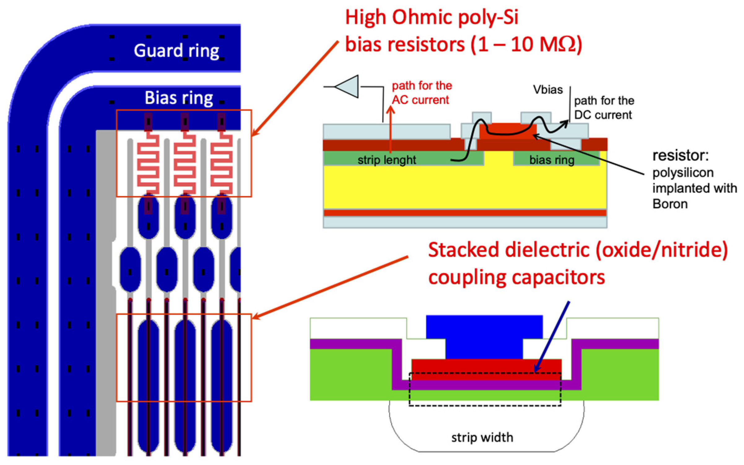
Additional components are sometimes necessary in detector technologies, especially for AC-coupled microstrip detectors. In fact, microstrips can be directly connected to the readout electronics (DC-coupled): the strip bias is provided by the front-end amplifier’s virtual ground. The amplifier should also sink the strip leakage current. However, in HEP experiments, the leakage current after irradiation can become very large, so it would be difficult for the amplifier to sink it without causing saturation effects. In this case, it is preferable to use AC-coupling through integrated capacitors realized on top of the strips (see Figure 4) [41]. In order to minimize the risk of shorts due to pin holes, capacitors are normally applied using a stacked dielectric layer (e.g., oxide + nitride) [42]. AC-coupling also requires a different biasing method, since the strips are not directly connected to the front-end amplifiers. For this purpose, the strips are typically connected through poly-Si resistors to a bias ring kept at ground level (see Figure 4) [43]. The target resistance of the poly-Si bias resistor is typically in the range of MΩs, i.e., large enough to reduce noise, but not too high to avoid significant voltage drop when leakage increases. Alternative bias techniques are based on punch-through or integrated transistors (the so-called FOXFET) [2].
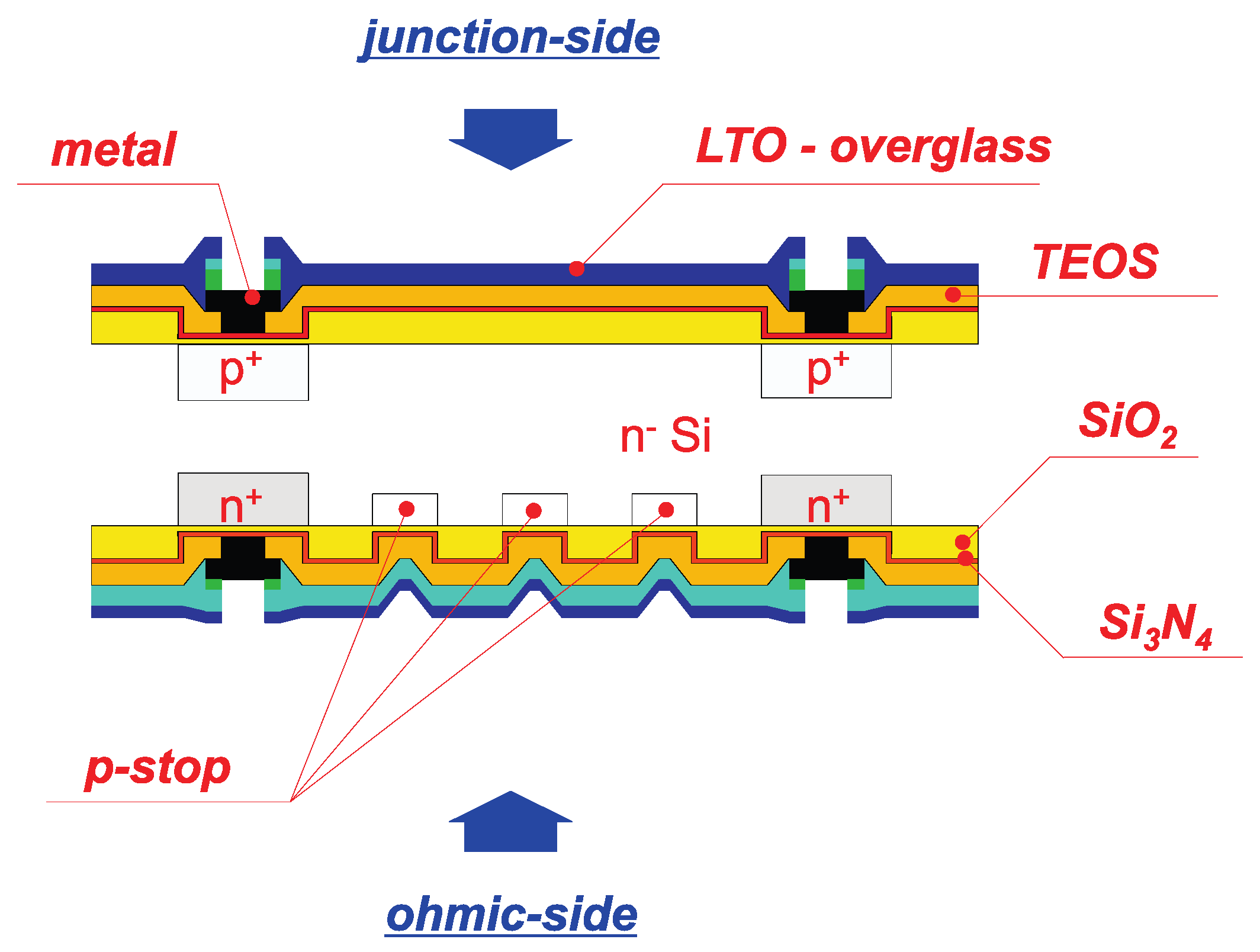
Needless to say, double-sided detectors involve a higher complexity as compared to single-sided ones, since both sides of the wafers must be patterned and processed [44]. One evident need is double-side alignment of different layers, calling for special lithography equipment. However, it should also be stressed that when one side of a wafer is treated, the other one should be protected from accidental damage (e.g., scratches) caused by the contact to the processing tools, which are typically not made for double-sided structures. Therefore, the number of process steps becomes more than double as compared to a single-sided process.
As an example, the schematic cross-section of a double-sided microstrip detector is reported in Figure 5, highlighting the different regions/materials involved. On the backside (n-side), it can be seen that p-stop regions are also included [45]. P-stops are patterned p-type implants ensuring surface isolation between adjacent n+ regions, which may otherwise be shorted by an electron accumulation layer at the Si/SiO2 interface caused by the positive oxide charge. Alternative solutions for surface isolation are p-spray, i.e., a blank low-dose p-type implant [46], or a combination of p-stop and p-spray [47].
3.2.3. Integrated Transistors
Starting from the late 1980s, several attempts were made to monolithically integrate part of the read-out electronics on the detector substrate, thus reducing the amount of material in the active detection area, relaxing the bonding constraints and most of all minimizing the parasitic capacitances associated with the detector–preamplifier interconnection, so as to achieve better noise performance. This is particularly important for detectors having very low capacitance (e.g., drift detectors).
The need to preserve the detector characteristics, especially low leakage current, represents a major technological constraint. Two different strategies have been pursued to face this problem. The first relies on minimizing high-temperature steps, leading to carrier-lifetime degradation through defect activation. The second exploits extrinsic-gettering techniques to preserve long carrier lifetimes by counteracting the detrimental effect of contaminants. While the first approach results in ad hoc processes, the second one allows for more standard fabrication procedures to be adopted, as demonstrated by the realization of CMOS-compatible detector technologies [48].
An n-channel JFET was proposed by V. Radeka et al. in 1989 [49], fully compatible with the detector fabrication process. In fact, it required three additional ion-implantations steps for the realization of the n+ source/drain regions, of the n-channel and of a p-type region underneath the n-channel acting as a barrier layer for the channel electrons. Only one annealing step was performed at low temperature for the activation of the implanted dopants and for damage recovery; however, in order for the n-channel and p-type layer doping profiles to be located at a proper depth into the n-type high-resistivity substrate, high-energy ion implantations had to be used, which are not available in most processing facilities. Using such a device, a charge sensitive amplifier was successfully implemented on high-resistivity silicon [50]. A p-channel version of this JFET was also fabricated to be embedded in the anode of a silicon drift detector [51].
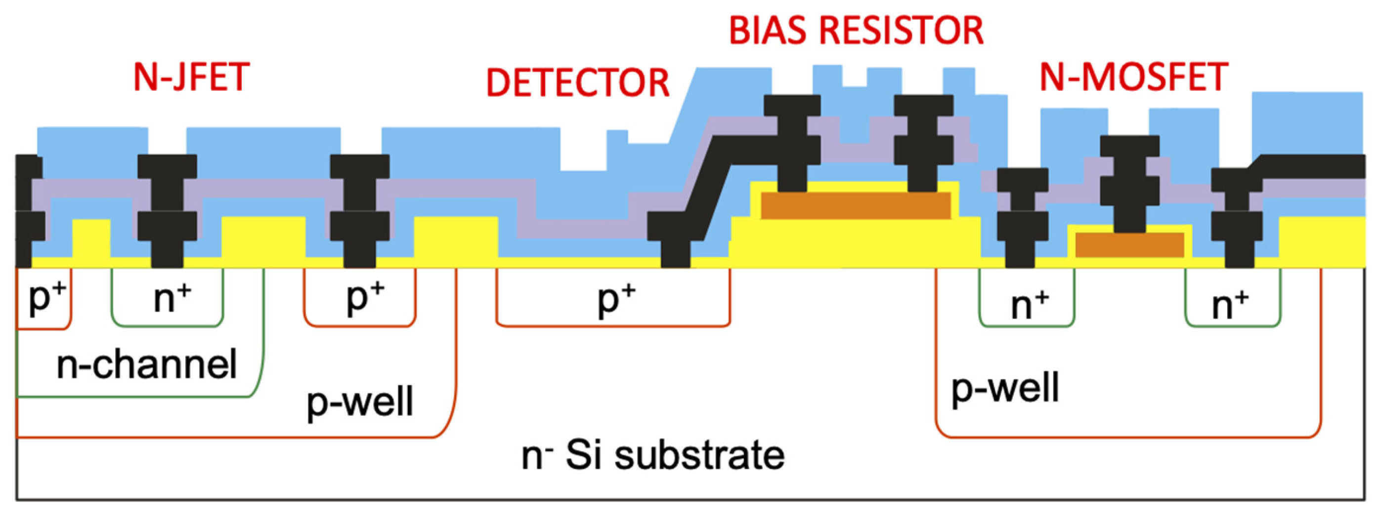
A special technology (JSD) has also been developed at FBK relying on back-side poly-Si gettering to keep the leakage current very low and allowing for the fabrication of different transistor types (n-JFETs, n-MOSFETs) and passive components (capacitors and resistors) [52,53]. As an example, Figure 6 shows the schematic cross-section of devices available within JSD technology, where the transistors are effectively shielded from the high-resistivity substrate by using a p-well, thus resulting in good saturating behavior and low-noise figures. Integrated JFET/MOSFET charge-sensitive amplifiers were made with JSD technology [54]. A simplified version of this process, featuring a different profile for the p-well, has been used for the fabrication of high-gain bipolar transistors [55], which eventually found a suitable application for the detection of Radon gas [56].
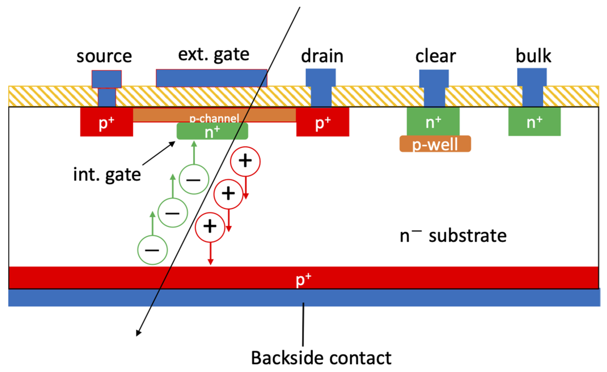
Among detector-compatible transistors, the most important device is certainly the DePFET, which was first conceptually proposed by J. Kemmer and G. Lutz in 1987 [57]. A sketch of the device is shown in Figure 7. Similar to drift detectors, DePFETs also exploit sideward depletion, so that a potential valley for electrons can be obtained inside the active volume and, depending on the applied voltages, actually located underneath the transistor channel at the so-called internal gate. By doing so, the electrons collected at the internal gate can modulate the current in the transistor, making the DePFET a radiation detector and a front-end transistor at the same time, with outstanding noise performance [58]. Since the electrons are stored in the internal gate (until removed using a clear mechanism), the read-out of DePFET signals are non-destructive, and multiple readings can further average noise, leading to outstanding values even below 1 electron r.m.s. [59]. The DSSC (DePFET Sensor with Signal Compression) is an evolution of the DePFET featuring multiple implants to create an “overflow” region for the internal gate; this device is aimed at X-ray Free Electron Laser applications, where a very large dynamic range is requested [60]. Nowadays, DePFET represents an appealing solution for many applications in particle physics and X-ray imaging. A comprehensive overview can be found in [61].
3.2.4. Avalanche-Based Detectors
A recent development in silicon radiation detectors, and one of the topics of most interest presently, are low-gain avalanche detectors (LGADs) [62]. LGADs are detectors with intrinsic amplification, based on impact ionization effects, similar to avalanche photodiodes (APDs) but revisited for the detection of ionizing radiation, and mainly for high-energy-charged particles in HEP experiments. In future experiments at hadron colliders, the pile up will be so high so as to make the particle tracks undistinguishable unless the time information is added to the hit position. LGADs are made on thin substrates (a few tens of micrometers), and can deliver very fast signals, boosted by the internal gain, so they can obtain very good timing resolution, of the order of 20 ps [63]. Compared to standard APDs, LGADs are designed to yield a lower gain of at most a few tens, which is enough to compensate for signal loss due to charge trapping and to the use of thin substrates, while limiting the excess noise factor [64]. A comprehensive treatment of LGADs can be found in [65].
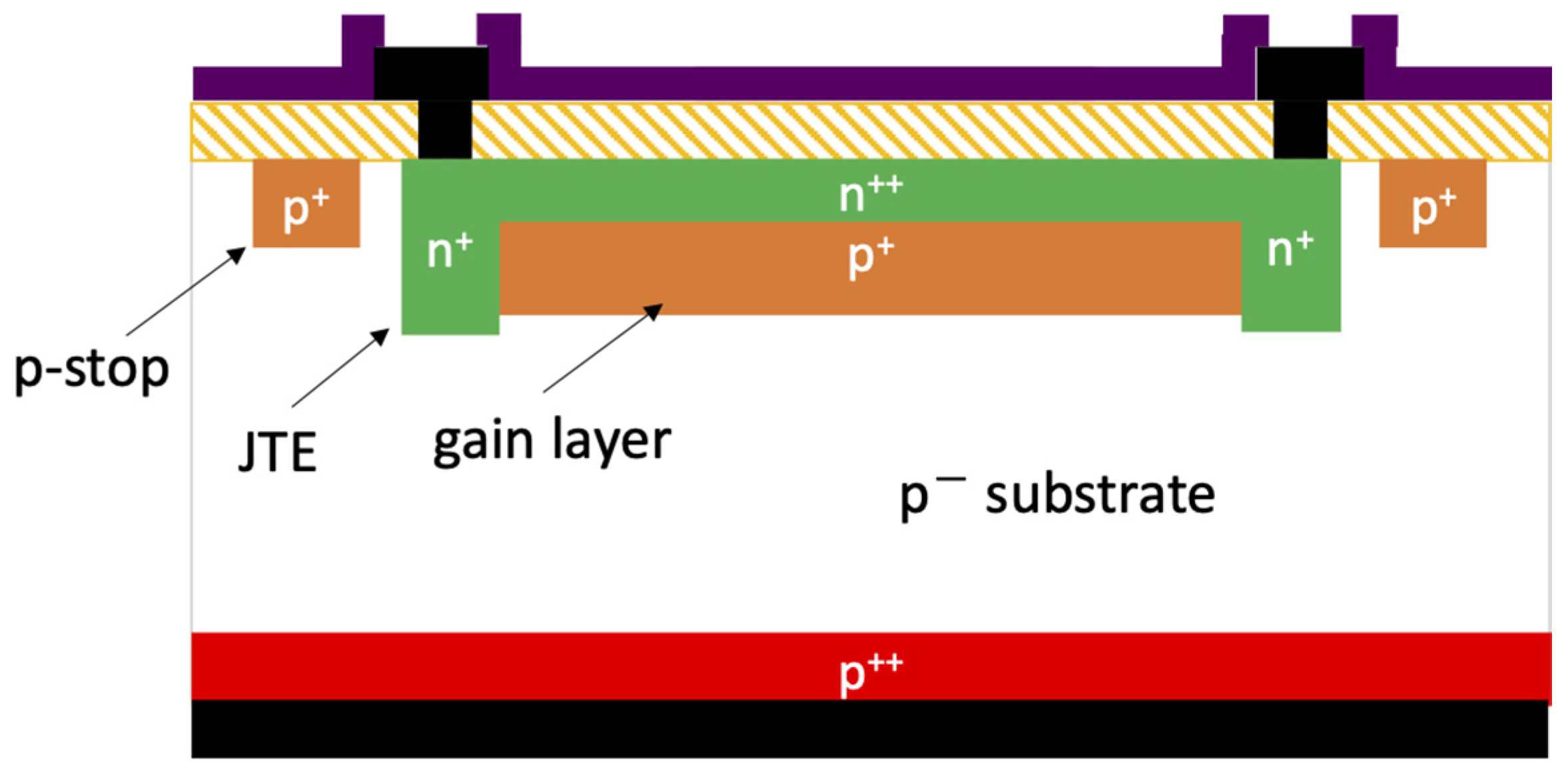
LGADs were first developed at CNM [66] and are currently available from several processing facilities. A schematic cross-section of the device is shown in Figure 8. A high-resistivity p-type substrate is used, with signal readout from the n++ regions. Compared to standard detectors, an additional p+ layer, referred to as gain layer, is implanted beneath the n++ region to control the avalanche multiplication mechanism. The dose of the gain layer and its doping profile should be optimized to yield the best trade-off between the gain and the breakdown voltage.
As shown in Figure 8, the device also features a junction termination consisting of a deep n+ region equipped with a metal field plate, the so-called JTE (typical of power devices), aimed at preventing from early breakdown at the edge, as well as a p-stop region, aimed at isolating adjacent n+ regions at the surface. The latter structures introduce a no-gain region, and in the case of arrays of LGADs, they can limit the geometrical efficiency (i.e., the fill factor) [67]. This is not a major issue in LGAD arrays for the timing layers of ATLAS and CMS detectors, which have a rather large pitch of 1.3 mm [68], but it could become significant in future experiments calling for higher spatial resolution. Several solutions have been proposed to address this problem and are currently being developed. Among them are double-sided LGADs [69], commonly referred to as inverse LGADs (iLGADs) [70], which feature a large, uniform multiplication region on the side opposite to the pixelated one. An unsegmented gain layer is also present in AC-LGADs [71,72], where segmented metal pads are capacitively coupled to the detector substrate through a thin dielectric layer. In order to reduce the non-negligible cross-talk observed in AC-LGAD, a design variant has been proposed, the so-called DC-coupled resistive silicon detectors, where readout n+ implants are embedded into the uniform n-resistive layer [73]. Another interesting approach aimed at minimizing the no-gain region while retaining the original LGAD structure is the trench-isolated LGAD [74], where the JTE and the p-stop are replaced by narrow trenches, thus reducing the interpixel dead area to just a few micrometers.
Another relevant problem with LGADs is their limited radiation hardness, due to the vanishing of the gain after large irradiation fluences, of the order of ~1015 neq/cm2 [75], an effect which has been ascribed to the radiation induced de-activation of Boron in the gain layer (aka “acceptor removal”). Among possible solutions to attenuate this problem are the gain layer profile engineering and the co-implantation of carbon ions [76,77].
Besides HEP applications, LGADs are gaining an increasing importance in photon science for soft X-ray imaging. New X-ray free electron lasers (FELs) worldwide provide unique scientific imaging opportunities in the soft X-ray energy range from 250 eV to 1.5 keV. Low-energy X-rays produce signals with amplitude lower than the noise floor of the readout chip, calling for internal amplification in the sensor, which can be achieved with LGADs [78]. Besides a high fill factor, the LGAD technology for this application requires a thin entrance window to allow for low-energy X-rays to reach the active volume of the silicon sensor [79].
3.3. 3D Technology
In the mid-1990s, Sherwood Parker and his collaborators introduced 3D detectors [80]. These detectors are distinct from planar detectors because they incorporate vertical electrodes (typically cylindrical) of both doping types, which are oriented perpendicular to the wafer surface and extend deep into the substrate. This design allows for a significantly smaller interelectrode distance than the detector’s active thickness, resulting in several advantages over planar detectors:
- (i)
- The full depletion voltage is much lower: before irradiation, a 3D detector can be efficiently operated at a bias of just a few Volts, and even after irradiation up to very large fluences of the order of ~1016 neq/cm2, the required bias voltage is still limited to ~150 V. Since the leakage current after irradiation can become very large, the related reduction in the power dissipation is very important;
- (ii)
- The time response is much faster: the total signal duration is typically below 1 ns, with rise times below 100 ps, leading to outstanding results in the timing resolution (a few tens of ps);
- (iii)
- Charge-trapping effects, which represent the most important limitation to the signal efficiency after large irradiation fluences, can be strongly attenuated, making 3D detectors the most radiation-hard silicon detectors;
- (iv)
- The extension of the dead region at the detector periphery, which in planar detectors is typically a few hundreds of micrometers, can be minimized to just a few μm by using deep trench terminations, the so-called “active edges”;
- (v)
- Three-dimensional structures with high aspect-ratio cavities filled by proper converter materials (e.g., 6LiF or 10B) can be used for thermal neutron detection and imaging with high efficiency, up to ~50%, owing to the increased surface area of the silicon sensors where the neutron converter material is deposited [81,82,83,84];
- (vi)
- Very small detection volumes can be accurately defined in 3D structures, as requested for microdosimetry in synchrotron and particle therapy and space radiation protection [85].
Besides the technological complexity, with related cost and yield issues, 3D detectors have some functional disadvantages: (i) the signal response is spatially non-uniform, due to the electrodes themselves (dead regions) and to other low-field regions in between electrodes of the same doping type; (ii) the capacitance is much larger than in planar detectors (a factor from 2 to 5, depending on the thickness), due to the depth of the electrodes and the small spacing between them. Although in principle several types of detectors (e.g., pixel, strip, pad, etc.) can be arranged by different connections of the electrodes at the surface, the problem of large capacitance limits the practical use of 3D detectors to pixel detectors only. A comprehensive treatment of 3D detectors can be found in [86] and up-to-date information in [87].
Three-dimensional detector technology is based on a combination of microelectronics and MEMS technologies, where deep reactive ion etching (DRIE) by the Bosch process [88] is the key step: using advanced DRIE equipment, it is possible to realize vertical electrodes with a high aspect ratio (electrode depth to diameter) of more than 25:1. Currently, there are two possible approaches: single-sided 3D and double-sided 3D.
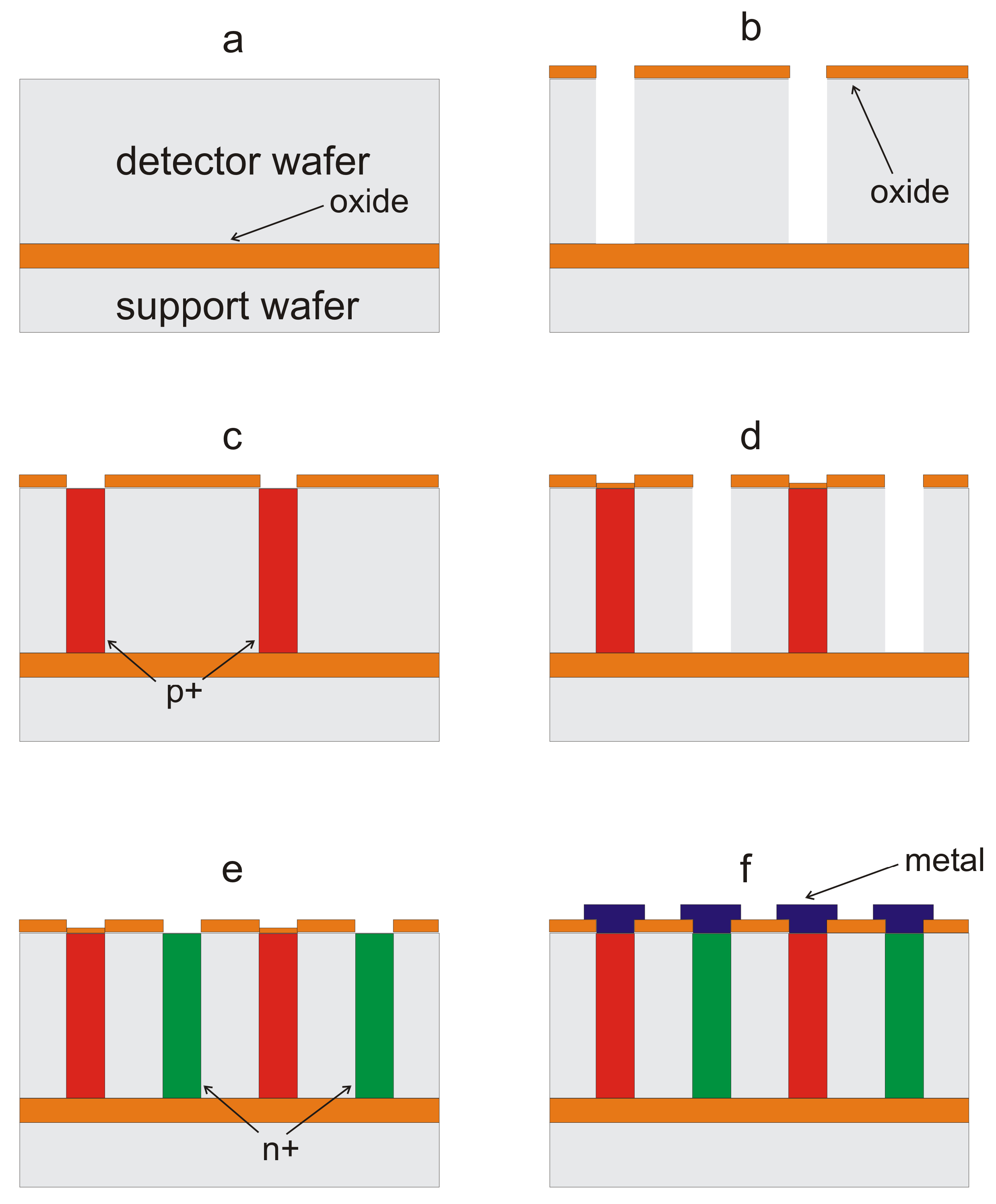
The first 3D detectors were made in Stanford [89] using a single-sided 3D process (see Figure 9). A high-resistivity sensor wafer is oxide bonded to a support wafer for mechanical stability [90]. A p-spray layer is present at both surfaces of the sensor wafer to ensure isolation between the n+ (readout) columns. The column etching is performed from the front side of the sensor wafer for both types of electrodes, starting from the p+ (ohmic) ones. The columns are etched all through the sensor wafer, stopping when the bonding oxide is reached. Columns are completely filled with doped poly-Si. Metal is finally deposited and patterned.
Additional steps, not shown in Figure 9, are required for active edges [91]: one of the two DRIE steps can be used to etch one set of columns and border trenches at the same time, provided the trench width is narrower than the column diameter, so that the etch rates are comparable. Trenches should also be filled with poly-Si and doped like columnar electrodes. An additional DRIE step is finally required to etch all the material surrounding the detector, while leaving a few micrometers of poly-Si to protect the sensor edge from mechanical damage and contamination from impurities (see Figure 10).
It should be mentioned that active edges have later been successfully implemented in planar sensors in the so-called “planar active-edge” (or edgeless) configuration. In these detectors, the readout electrodes are arranged by standard planar design, but the active area is terminated by deep trenches etched by DRIE and doped to act as (normally ohmic) electrodes [92]. The approach for the realization of trenches at most processing facilities is the same as previously described for 3D detectors, apart from the Technical Research Centre of Finland (VTT), which has developed an original process on 6-inch wafers where four-quadrant edge implantation is used for trench doping [93]. For many applications of planar sensors with active edge, the support wafer should be removed after completing the sensor fabrication. This post-processing step has been shown to be challenging and should be properly combined with the interconnect technology between sensor and readout electronics. It is worth mentioning that a support wafer-free processing method has been recently demonstrated [94].
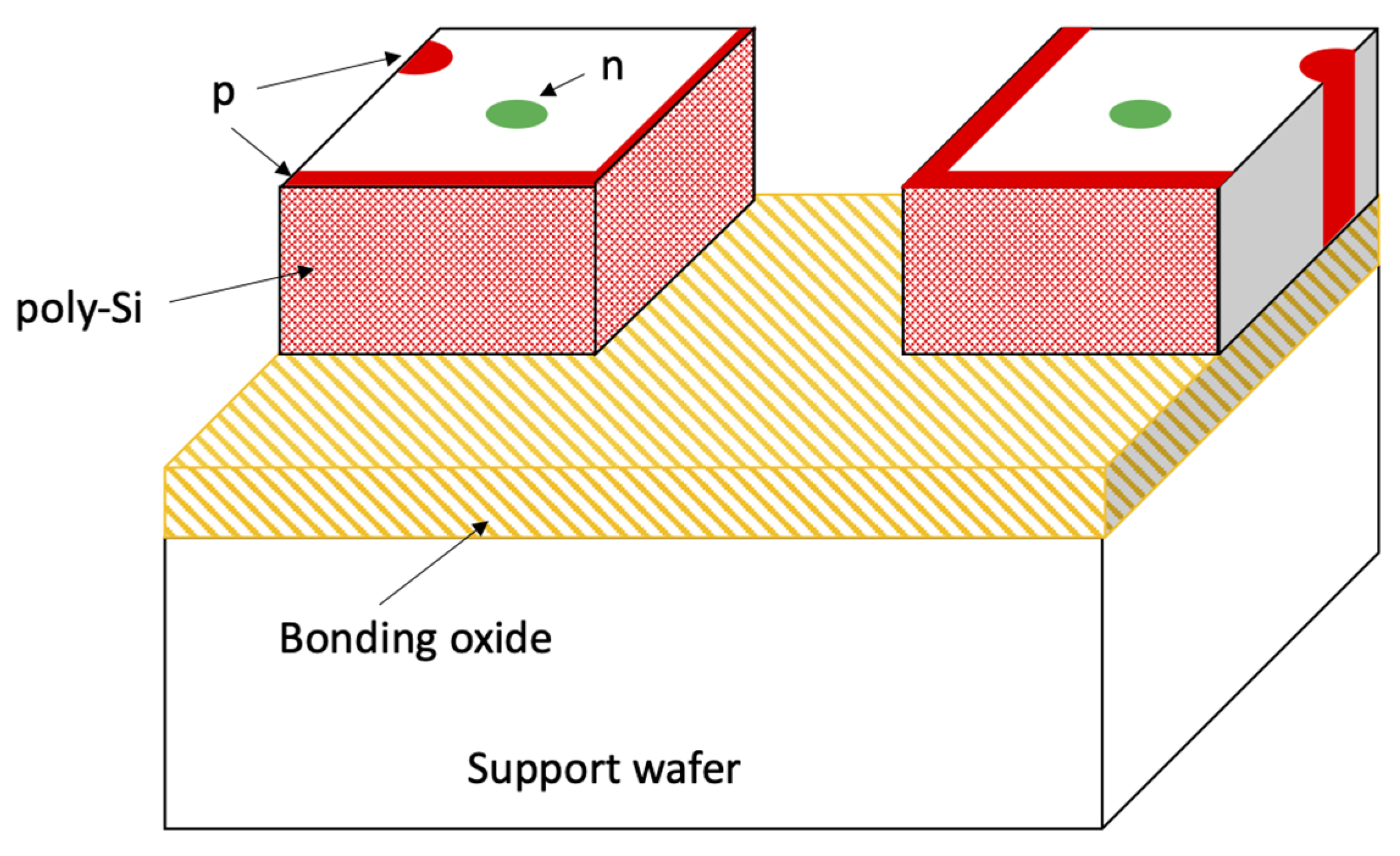
The double-sided 3D process (see Figure 11) was independently proposed by CNM (Barcelona, Spain) [95] and FBK (Trento, Italy) [96] in two slightly different flavors. The n+ (readout) column etching is performed from one side, and the p+ (ohmic) column etching from the other one, stopping at a short distance from the opposite surface. A full passing-through version of the process was also developed by FBK [97]. The absence of a support wafer and related need for oxide bonding and final removal largely simplifies the process. In addition, as compared to the original 3D detectors from Stanford, sensors made at CNM and FBK had narrower columns, which did not require to be completely filled with poly-Si while preserving a smooth surface topography. As a result, double-sided technologies are simpler, leading to shorter processing time, an advantage that motivated their adoption for the ATLAS Insertable B-Layer (IBL), the first application of 3D technology in an HEP experiment [98]. Due to the absence of a support wafer, an evident disadvantage of double-sided 3D detectors is that active edges are not readily available. However, 3D technology still provides an interesting alternative, the so-called “slim edges”, which consist in a multiple fence of p+ columns around the active area, confining the spread of the depletion region from the outermost pixels to few tens of μm, so that the dead area at the edge can be limited to ~100 μm [99].
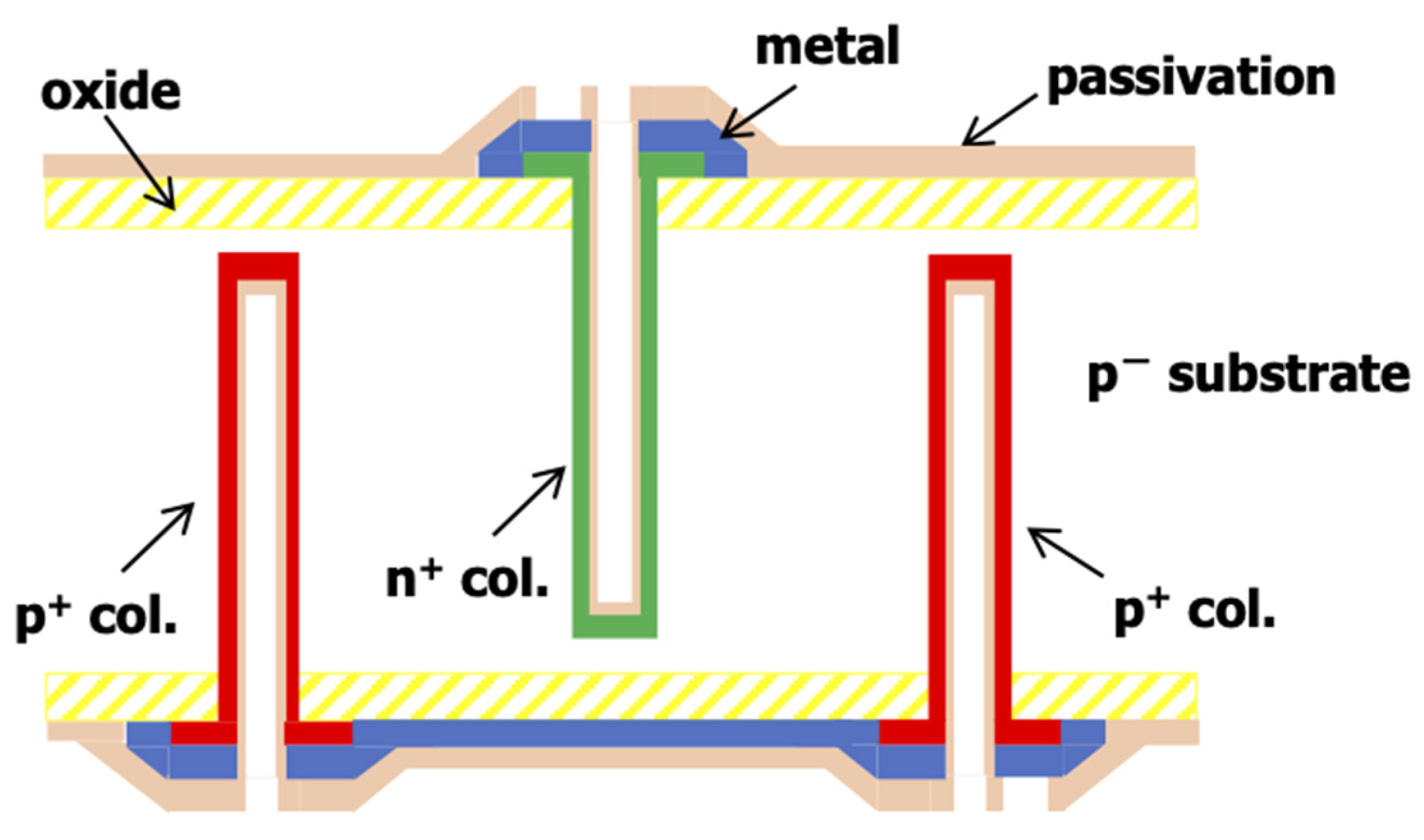
Following the IBL installation, a new generation of 3D pixels has been developed aimed at the innermost layers of the ATLAS [100] and CMS [101] detector upgrades at the high-luminosity LHC. These new pixel detectors have a much smaller size (50 × 50 and 25 × 100 μm2) and smaller active thickness (150 μm) than the previous ones. In particular, the smaller thickness prevents the use of double-sided technologies due to mechanical fragility issues. Hence, the single-sided process was resumed, with a significant modification, proposed by FBK and later adopted by other interested foundries, consisting in the use of Si-Si direct wafer-bonded (DWB) substrates, consisting of a high-resistivity sensor wafer bonded to a low-resistivity support wafer without an oxide layer in between them [102]. A schematic cross-section of a 3D detector made in this technology is shown in Figure 12. The etching of the n+ (readout) columns stops at a short distance (~20 μm) from the highly doped support wafer to prevent early breakdown. On the contrary, the p+ (bias) columns are etched through the high-resistivity sensor wafer and penetrate the support wafer, thus making good ohmic contact. By doing so, the bias can be applied from the backside after thinning the support wafer and depositing a metal layer. The last steps are preferably performed as a post-processing combined with the bump bonding interconnect process.
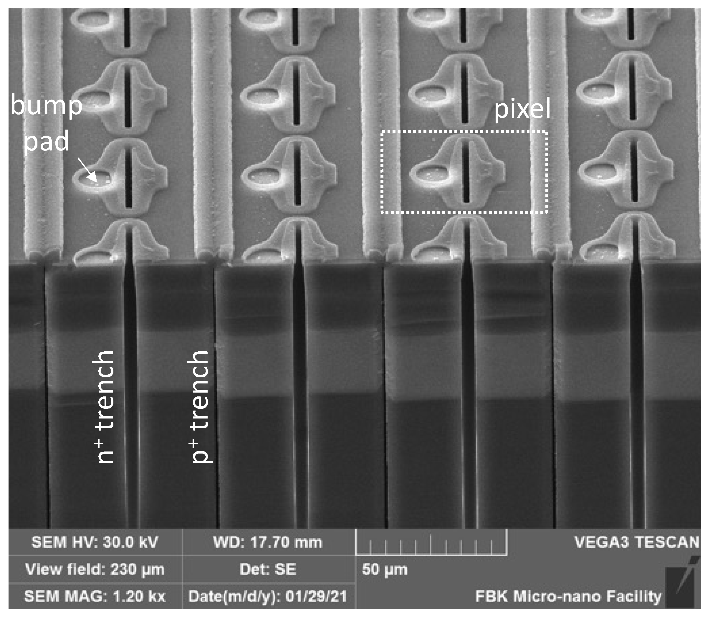
Another recent development in 3D detectors is the use of trenched electrodes, aimed at improving the timing resolution, owing to a better uniformity in the electric field and weighting field distributions, as originally proposed by S. Parker in [103]. Within the INFN TIMESPOT project, 3D-trenched pixel detectors have been realized for the first time [104], and considerable results in terms of timing resolution, close to 10 ps, have already been reported [105,106]. These detectors are made using a single-sided technology like that used for small-pitch 3D pixels [107]. As an example, Figure 13 shows a scanning electron microscope picture of a 3D-trench pixel detector made at FBK. A common feature characterizing the most recent versions of 3D detectors, both based on columns and on trenches, is the small pixel size, resulting in rather dense layouts and calling for better resolution in the lithography process. To this purpose, FBK has started using stepper lithography in place of a standard mask aligner, which allows for high alignment accuracy and a good definition of the sensor geometries also in the most critical layouts [108].
4. Conclusions
We have summarized the main developments in silicon radiation detectors through their ~40 year-long history, reviewing the most important types of devices with emphasis on fabrication issues. Detector technology has reached a level of maturity, but it still possesses unique characteristics that make it better suited for implementation in specialized processing facilities focused on research and development. One of the main drivers in the progress of silicon detectors has always been the field of high energy physics with its ever-increasing demand for performance and reliability. At present, topics of significant interest are ultra-fast detectors, aimed at future experiments at high-luminosity, high-energy particle colliders, for which outstanding timing resolution, in the order of 10s of ps, will be necessary, along with the already excellent position resolution. There is growing interest in detectors that offer exceptional timing resolution, such as those utilizing intrinsic amplification through the avalanche effect (LGADs) or those with three-dimensional electrodes (3D detectors). The emergence of CMOS monolithic pixels (not covered in this paper) is expected to gradually replace some conventional detectors in HEP experiments and X-ray imaging applications, but specialized detectors will continue to be indispensable.
Author Contributions
The manuscript was written and reviewed by G.-F.D.B. and J.Y. All authors have read and agreed to the published version of the manuscript.
Funding
This research was partially funded by the Italian National Institute for Nuclear Physics (INFN), CSN1 (Project FASE_ATLAS) and CSN5 (Project TIMESPOT).
Institutional Review Board Statement
Not applicable.
Informed Consent Statement
Not applicable.
Data Availability Statement
Not applicable.
Acknowledgments
Conflicts of Interest
The authors declare no conflict of interest.
References
- Knoll, G.F. Radiation Detection and Measurement, 4th ed.; Wiley: New York, NY, USA, 2010. [Google Scholar]
- Lutz, G. Semiconductor Radiation Detectors–Device Physics, 2nd ed.; Springer: Berlin/Heidelberg, Germany, 2007. [Google Scholar]
- Marco-Hernández, R. Overview of CMOS sensors for future tracking detectors. Instruments 2020, 4, 36. [Google Scholar] [CrossRef]
- Ramo, S. Currents induced by electron motion. Proc. IRE 1939, 27, 584–585. [Google Scholar] [CrossRef]
- Goulding, F.S.; Hansen, W.L. Leakage current in semiconductor junction radiation detectors and its influence on energy-resolution characteristics. Nuclear Instrum. Methods 1961, 12, 249–262. [Google Scholar] [CrossRef] [Green Version]
- Da Rold, M.; Bacchetta, N.; Bisello, D.; Paccagnella, A.; Dalla Betta, G.F.; Verzellesi, G.; Verdini, P.G. Study of breakdown effects in silicon multiguard structures. IEEE Trans. Nucl. Sci. 1999, 46, 1215–1223. [Google Scholar] [CrossRef]
- Moll, M. Displacement Damage in Silicon Detectors for High Energy Physics. IEEE Trans. Nucl. Sci. 2018, 65, 1561–1582. [Google Scholar] [CrossRef]
- Ma, T.P.; Dressendorfer, P.V. Ionizing Radiation Effects in MOS Devices and Circuits, 1st ed.; Wiley: New York, NY, USA, 1989. [Google Scholar]
- Zhang, J.; Fretwurst, E.; Klanner, R.; Pintilie, I.; Schwandt, J.; Turcato, M. Investigation of X-ray induced radiation damage at the Si-SiO2 interface of silicon sensors for the European XFEL. J. Instrum. 2012, 7, C12012. [Google Scholar] [CrossRef] [Green Version]
- Von Ammon, W.; Herzer, H. The production and availability of high resistivity silicon for detector applications. Nuclear Instrum. Methods 1984, 226, 94–102. [Google Scholar] [CrossRef]
- Dreier, P. High resistivity silicon for detector applications. Nuclear Instrum. Methods 1990, 288, 272–277. [Google Scholar] [CrossRef]
- Lindström, G.; Moll, M.; Fretwurst, E. The RD48 Collaboration. Radiation hardness of silicon detectors–A challenge from high energy physics. Nuclear Instrum. Methods A 2001, 426, 1–15. [Google Scholar] [CrossRef]
- Seidel, S. Silicon strip and pixel detectors for particle physics experiments. Phys. Rep. 2019, 828, 1–34. [Google Scholar] [CrossRef]
- Landi, G.; Landi, G.E. Silicon micro-strip detectors. Encyclopedia 2021, 1, 1076–1083. [Google Scholar] [CrossRef]
- Straver, J.; Toker, O.; Weilhammer, P.; Colledani, C.; Dulinski, W.; Turchetta, R.; Bosisio, L. One micron spatial resolution with silicon strip detectors. Nuclear Instrum. Methods A 1994, 348, 485–490. [Google Scholar] [CrossRef] [Green Version]
- Batignani, G.; Bosi, F.; Bosisio, L.; Conti, A.; Focardi, E.; Forti, F.; Giorgi, M.; Parrini, G.; Scarlini, E.; Tempesta, P.; et al. Double-sided readout silicon strip detectors for the ALEPH minivertex. Nuclear Instrum. Methods A 1989, 277, 147–153. [Google Scholar] [CrossRef]
- Unno, Y.; Abo, Y.; Affolder, A.; Allport, P.; Bloch, I.; Blue, A.; Fadeyev, V.; Fernandez-Tejero, J.; Gregor, I.; Haber, C.; et al. ATLAS17LS–A large-format prototype silicon strip sensor for long-strip barrel section of ATLAS ITk strip detector. Nuclear Instrum. Methods 2021, 989, 164928. [Google Scholar] [CrossRef]
- Bergauer, T.; Dragicevic, M.; König, A.; Hacker, J.; Bartl, U. First thin AC-coupled silicon strip sensors on 8-inch wafers. Nuclear Instrum. Methods 2016, 830, 473–479. [Google Scholar] [CrossRef]
- Riedler, P.; Anelli, G.; Antinori, F.; Badalà, A.; Bruno, G.; Burns, M.; Cali, I.; Campbell, M.; Caselle, M.; Ceresa, S.; et al. Production and Integration of the ALICE Silicon Pixel Detector. Nuclear Instrum. Methods 2007, 572, 128–131. [Google Scholar] [CrossRef]
- Pitzl, D.; Cartiglia, N.; Hubbard, B.; Hutchinson, D.; Leslie, J.; O’Shaughnessy, K.; Rowe, W.; Sadrozinski, H.-W.; Seiden, A.; Spencer, E.; et al. Type inversion in silicon detectors. Nuclear Instrum. Methods 1992, 311, 98–104. [Google Scholar] [CrossRef]
- Affolder, A.; Allport, P.; Casse, G. Charge Collection Efficiency measurements of heavily irradiated segmented n-in-p and p-in-n silicon detectors for use at the Super-LHC. IEEE Trans. Nucl. Sci. 2009, 56, 765–770. [Google Scholar] [CrossRef]
- Affolder, A.; Allport, P.; Casse, G. Charge collection efficiencies of planar silicon detectors after reactor neutron and proton doses up to 1.6 × 10¹⁶ neq cm−2. Nuclear Instrum. Methods 2010, 612, 470–473. [Google Scholar] [CrossRef]
- Hügging, F.; Gößling, C.; Klaiber-Lodewigs, J.; Wüstenfeld, J.; Wunstorf, R. Prototype performance and design of the ATLAS pixel sensors. Nucl. Instrum. Methods 2001, 465, 77–82. [Google Scholar] [CrossRef]
- Allkofer, Y.; Amsler, C.; Bortoletto, D.; Chiochia, V.; Cremaldi, L.; Cucciarelli, S.; Dorokhov, A.; Hörmann, C.; Horisberger, R.; Kim, D.; et al. Design and performance of the silicon sensors for the CMS barrel pixel detector. Nucl. Instrum. Methods 2008, 584, 25–41. [Google Scholar] [CrossRef] [Green Version]
- Rossi, L.; Fischer, P.; Rohe, T.; Wermes, N. Pixel Detectors–From Fundamentals to Applications, 1st ed.; Springer: Berlin-Heidelberg, Germany, 2006. [Google Scholar]
- Battaglia, M.; Da Viá, C.; Bortoletto, D.; Brenner, R.; Campbell, M.; Collins, P.; Dalla Betta, G.-F.; Demarteau, M.; Denes, P.; Graafsma, H.; et al. R&D paths of pixel detectors for vertex tracking and radiation imaging. Nucl. Instrum. Methods 2013, 716, 29–45. [Google Scholar]
- Gatti, E.; Rehak, P. Semiconductor drift chamber-an application of a novel charge transport scheme. Nucl. Instrum. Methods 1984, 225, 608–614. [Google Scholar] [CrossRef] [Green Version]
- Gatti, E.; Rehak, P.; Walton, J. Silicon drift chambers-first results and optimum processing of the signal. Nucl. Instrum. Methods 1984, 226, 129–141. [Google Scholar] [CrossRef]
- Rehak, P.; Gatti, E.; Longoni, A.; Kemmer, J.; Holl, P.; Klanner, R.; Lutz, G.; Wylie, A. Semiconductor drift chambers for position and energy measurements. Nucl. Instrum. Methods 1985, 235, 224–234. [Google Scholar] [CrossRef]
- Hartmann, R.; Strüder, L.; Kemmer, J.; Lechner, P.; Fries, O.; Lorenz, E.; Mirzoyan, R. Ultrathin entrance windows for silicon drift detectors. Nucl. Instrum. Methods 1997, 387, 250–254. [Google Scholar] [CrossRef]
- Segal, J.; Kenney, C.; Kowalski, J.M.; Blaj, G.; Rozario, L.; Hasi, J.; Dragone, A.; Caragiulo, P.; Rota, L. Thin-entrance window process for soft X-ray sensors. Front. Phys. 2021, 9, 618390. [Google Scholar] [CrossRef]
- Bertuccio, G.; Ahangarianabhari, M.; Graziani, C.; Macera, D.; Shi, Y.; Gandola, M.; Rachevski, A.; Rashevskaya, I.; Vacchi, A.; Zampa, G.; et al. X-ray Silicon Drift Detector–CMOS front-end system with high energy resolution at room temperature. IEEE Trans. Nucl. Sci. 2016, 63, 400–406. [Google Scholar] [CrossRef]
- Rehak, P.; Gatti, E.; Longoni, A.; Sampietro, M.; Holl, P.; Lutz, G.; Kemmer, J.; Prechtel, U.; Ziemann, T. Spiral silicon drift detectors. IEEE Trans. Nucl. Sci. 1989, 36, 203–209. [Google Scholar] [CrossRef] [Green Version]
- Rashevsky, A.; Bonvicini, V.; Vacchi, A.; Zampa, N.; Burger, P.; Beole, S.; Idzik, M.; Petta, C.; Randazzo, N. Silicon drift detector with a continuous implanted resistor as divider-drift electrode. Nucl. Instrum. Methods 1998, 409, 210–215. [Google Scholar] [CrossRef]
- Jiang, S.; Jia, R.; Tao, K.; Wu, Y.; Liu, S. High-resistance voltage dividers fabricated by thin polysilicon films in silicon drift detectors. J. Mater. Sci. Mater. Electron. 2019, 30, 6617–6627. [Google Scholar] [CrossRef]
- Kemmer, J. Fabrication of low noise silicon radiation detectors by the planar process. Nucl. Instrum. Methods 1980, 169, 499–502. [Google Scholar] [CrossRef]
- Kemmer, J.; Burger, P.; Henck, R.; Heijne, E. Performance and applications of passivated ion-implanted silicon detectors. IEEE Trans. Nucl. Sci. 1982, 29, 733–737. [Google Scholar] [CrossRef]
- Kemmer, J. Improvement of detector fabrication by the planar process. Nucl. Instrum. Methods 1984, 226, 89–93. [Google Scholar] [CrossRef]
- Holland, S. An IC compatible detector process. IEEE Trans. Nucl. Sci. 1989, 36, 283–289. [Google Scholar] [CrossRef] [Green Version]
- Dalla Betta, G.; Pignatel, G.; Verzellesi, G.; Boscardin, M. Si-PIN X-ray detector technology. Nucl. Instrum. Methods A 1997, 395, 344–348. [Google Scholar] [CrossRef]
- Caccia, M.; Evensen, L.; Hansen, T.E.; Horisberger, R.; Hubbeling, L.; Peisert, A.; Zalewska, A. A Si strip detector with integrated coupling capacitors. Nucl. Instrum. Methods 1987, 260, 124–131. [Google Scholar] [CrossRef] [Green Version]
- Dalla Betta, G.-F.; Boscardin, M.; Bosisio, L. A comparative evaluation of integrated capacitors for AC-coupled microstrip detectors. Nucl. Instrum. Methods A 1998, 411, 369–375. [Google Scholar] [CrossRef]
- Hietanen, I.; Lindgren, J.; Orava, R.; Tuuva, T.; Voutilainen, M.; Brenner, R.; Andersson, M.; Leinonen, K.; Ronkainen, H. Ion-implanted capacitively coupled silicon strip detectors with integrated polysilicon bias resistors processed on a 100 mm wafer. Nucl. Instrum. Methods A 1991, 310, 671–676. [Google Scholar] [CrossRef]
- Dalla Betta, G.-F.; Boscardin, M.; Bosisio, L.; Rachevskaia, I.; Zen, M.; Zorzi, N. Development of a fabrication technology for double-sided AC-coupled silicon microstrip detectors. Nucl. Instrum. Methods 2001, 460, 306–315. [Google Scholar] [CrossRef]
- Iwata, Y.; Ohsugi, T.; Fujita, K.; Kitabayashi, H.; Yamamoto, K.; Yamamura, K.; Unno, Y.; Kondo, T.; Terada, S.; Kohriki, T.; et al. Optimal p-stop pattern for the n-side strip isolation of silicon microstrip detectors. IEEE Trans. Nucl. Sci. 1998, 45, 303–309. [Google Scholar] [CrossRef]
- Richter, R. Strip detector design for ATLAS and HERA-B using two-dimensional device simulation. Nucl. Instrum. Methods 1996, 377, 412–421. [Google Scholar] [CrossRef]
- Piemonte, C. Device simulations of isolation techniques for silicon microstrip detectors made on p-type substrates. IEEE Trans. Nucl. Sci. 2006, 53, 1694–1705. [Google Scholar] [CrossRef]
- Holland, S. Properties of CMOS devices and circuits fabricated on high-resistivity, detector-grade silicon. IEEE Trans. Nucl. Sci. 1992, 39, 809–813. [Google Scholar] [CrossRef] [Green Version]
- Radeka, V.; Rahek, P.; Rescia, S.; Gatti, E.; Longoni, A.; Sampietro, M.; Bertuccio, G.; Holl, P.; Struder, L.; Kemmer, J. Implanted silicon JFET on completely depleted high-resistivity devices. IEEE Electron. Device Lett. 1989, 10, 91–94. [Google Scholar] [CrossRef]
- Rehak, P.; Rescia, S.; Radeka, V.; Gatti, E.; Longoni, A.; Sampietro, M.; Bertuccio, G.; Holl, P.; Strüder, L.; Kemmer, J.; et al. Feedback charge amplifier integrated on detector wafer. Nucl. Instrum. Methods A 1990, 288, 168–175. [Google Scholar] [CrossRef]
- Sampietro, M.; Fasoli, L.; Rehak, P.; Struder, L. Novel p-JFET embedded in silicon radiation detectors avoids preamplifier feedback resistor. IEEE Electron. Device Lett. 1995, 16, 208–210. [Google Scholar] [CrossRef]
- Dalla Betta, G.-F.; Boscardin, M.; Gregori, P.; Zorzi, N.; Pignatel, G.; Batignani, G.; Giorgi, M.; Bosisio, L.; Ratti, L.; Speziali, V.; et al. A fabrication process for silicon microstrip detectors with integrated front-end electronics. IEEE Trans. Nucl. Sci. 2002, 49, 1022–1026. [Google Scholar] [CrossRef]
- Dalla Betta, G.-F.; Batignani, G.; Boscardin, M.; Bosisio, L.; Gregori, P.; Pancheri, L.; Piemonte, C.; Ratti, L.; Verzellesi, G.; Zorzi, N. Monolithic integration of detectors and transistors on high-resistivity silicon. Nucl. Instrum. Methods A 2007, 579, 658–663. [Google Scholar] [CrossRef]
- Dalla Betta, G.-F.; Boscardin, M.; Fenotti, F.; Pancheri, L.; Piemonte, C.; Ratti, L.; Zorzi, N. Low noise Junction Field Effect Transistors in a silicon radiation detector technology. IEEE Trans. Nucl. Sci. 2006, 53, 3004–3012. [Google Scholar] [CrossRef]
- Bosisio, L.; Batignani, G.; Bettarini, S.; Boscardin, M.; Dalla Betta, G.-F.; Giacomini, G.; Piemonte, C.; Verzellesi, G.; Zorzi, N. Performance evaluation of radiation sensors with internal signal amplification based on the BJT effect. Nucl. Instrum. Methods 2006, 568, 217–223. [Google Scholar] [CrossRef]
- Rovati, L.; Bettarini, S.; Bonaiuti, M.; Bosisio, L.; Dalla Betta, G.-F.; Tyzhnevyi, V.; Verzellesi, G.; Zorzi, N. Alpha-particle detection based on the BJT detector and simple, IC-based readout electronics. J. Instrum. 2009, 4, P11010. [Google Scholar] [CrossRef]
- Kemmer, J.; Lutz, G. New detector concepts. Nucl. Instrum. Methods 1987, 253, 365–377. [Google Scholar] [CrossRef]
- Lutz, G. DEPFET development at the MPI semiconductor laboratory. Nuclear Instrum. Methods 2005, 549, 103–111. [Google Scholar] [CrossRef]
- Wolfel, S.; Herrmann, S.; Lechner, P.; Lutz, G.; Porro, M.; Richter, R.H.; Treis, J. A novel way of single optical photon detection: Beating the 1/f noise limit with ultra-high resolution DEPFET-RNDR devices. IEEE Trans. Nucl. Sci. 2007, 54, 1311–1318. [Google Scholar] [CrossRef]
- Lutz, G.; Lechner, P.; Porro, M.; Strüder, L.; De Vita, G. DEPFET sensor with intrinsic signal compression developed for use at the XFEL free electron laser radiation source. Nucl. Instrum. Methods 2010, 624, 528–532. [Google Scholar] [CrossRef]
- Andricek, L.; Bähr, A.; Lechner, P.; Ninkovic, J.; Richter, R.; Schopper, F.; Treis, J. DePFET–Recent developments and future prospects. Front. Phys. 2022, 10, 896212. [Google Scholar] [CrossRef]
- Giacomini, G. LGAD-Based Silicon Sensors for 4D Detectors. Sensors 2023, 23, 2132. [Google Scholar] [CrossRef]
- Cartiglia, N.; Staiano, A.; Sola, V.; Arcidiacono, R.; Cirio, R.; Cenna, F.; Ferrero, M.; Monaco, V.; Mulargia, R.; Obertino, M.; et al. Beam test results of a 16 ps timing system based on ultra-fast silicon detectors. Nucl. Instrum. Methods 2017, 850, 83–88. [Google Scholar] [CrossRef]
- McIntyre, R.J. Multiplication noise in uniform avalanche diodes. IEEE Trans. Electron. Dev. 1966, 13, 164–168. [Google Scholar] [CrossRef]
- Ferrero, M.; Arcidiacono, R.; Mandurrino, M.; Sola, V.; Cartiglia, N. An Introduction to Ultra-Fast Silicon Detectors, 1st ed.; CRC Press: Boca Raton, FL, USA, 2021. [Google Scholar]
- Pellegrini, G.; Fernández-Martínez, P.; Baselga, M.; Fleta, C.; Flores, D.; Greco, V.; Hidalgo, S.; Mandić, I.; Kramberger, G.; Quirion, D.; et al. Technology developments and first measurements of Low Gain Avalanche Detectors (LGAD) for high energy physics applications. Nucl. Instrum. Methods A 2014, 765, 12–16. [Google Scholar] [CrossRef]
- Giacomini, G. Fabrication of Silicon Sensors Based on Low-Gain Avalanche Diodes. Front. Phys. 2021, 9, 618621. [Google Scholar] [CrossRef]
- Cartiglia, N.; Arcidiacono, R.; Ferrero, M.; Mandurrino, M.; Sadrozinski, H.-F.; Sola, V.; Staiano, A.; Seiden, A. Timing layers: 4- and 5-dimensions tracking. Nucl. Instrum. Methods 2019, 924, 350–354. [Google Scholar] [CrossRef]
- Dall Betta, G.-F.; Pancheri, L.; Boscardin, M.; Paternoster, G.; Piemonte, C.; Cartiglia, N.; Cenna, F.; Bruzzi, M. Design and TCAD simulation of double-sided pixelated low gain avalanche detectors. Nucl. Instrum. Methods 2015, 796, 154–157. [Google Scholar] [CrossRef]
- Currás, E.; Carulla, M.; Vignali, M.C.; Duarte-Campderros, J.; Fernández, M.; Flores, D.; García, A.; Gómez, G.; González, J.; Hidalgo, S.; et al. Inverse Low Gain Avalanche Detectors. iLGADs) for precise tracking and timing applications. Nucl. Instrum. Methods A 2020, 958, 162545. [Google Scholar] [CrossRef] [Green Version]
- Giacomini, G.; Chen, W.; D’Amen, G.; Tricoli, A. Fabrication and performance of AC-coupled LGADs. J. Instrum. 2019, 14, P09004. [Google Scholar] [CrossRef] [Green Version]
- Mandurrino, M.; Arcidiacono, R.; Boscardin, M.; Cartiglia, N.; Dalla Betta, G.F.; Ferrero, M.; Ficorella, F.; Pancheri, L.; Paternoster, G.; Siviero, F.; et al. Tornago, M. Demonstration of 200-, 100-, and 50-mm pitch Resistive AC-coupled Silicon Detectors. RSD) with 100% fill-factor for 4D particle tracking. IEEE Electron. Device Lett. 2019, 40, 1780–1783. [Google Scholar] [CrossRef] [Green Version]
- Menzio, L.; Arcidiacono, R.; Borghi, G.; Boscardin, M.; Cartiglia, N.; Vignali, M.C.; Costa, M.; Dall Betta, G.-F.; Ferrero, M.; Ficorella, F.; et al. DC-coupled resistive silicon detectors for 4D tracking. Nucl. Instrum. Methods A 2022, 1041, 167374. [Google Scholar] [CrossRef]
- Paternoster, G.; Borghi, G.; Boscardin, M.; Cartiglia, N.; Ferrero, M.; Ficorella, F.; Siviero, F.; Gola, A.; Bellutti, P. Trench-Isolated low gain avalanche diodes. TI-LGADs. IEEE Electron. Device Lett. 2020, 41, 884–887. [Google Scholar] [CrossRef]
- Kramberger, G.; Baselga, M.; Cindro, V.; Fernández-Martínez, P.; Flores, D.; Galloway, Z.; Gorišek, A.; Greco, V.; Hidalgo, S.; Fadeyev, V.; et al. Radiation effects in Low Gain Avalanche Detectors after hadron irradiations. J. Instrum. 2015, 10, P07006. [Google Scholar] [CrossRef]
- Ferrero, M.; Arcidiacono, R.; Barozzi, M.; Boscardin, M.; Cartiglia, N.; Dalla Betta, G.; Galloway, Z.; Mandurrino, M.; Mazza, S.; Paternoster, G.; et al. Radiation resistant LGAD design. Nucl. Instrum. Methods 2019, 919, 16–26. [Google Scholar] [CrossRef]
- Li, M.; Fan, Y.; Jia, X.; Cui, H.; Liang, Z.; Zhao, M.; Yang, T.; Wu, K.; Li, S.; Yu, C.; et al. Effects of shallow carbon and deep N++ layer on the radiation hardness of IHEP-IME LGAD sensors. IEEE Trans. Nucl. Sci. 2022, 69, 1098–1103. [Google Scholar] [CrossRef]
- Andrä, M.; Zhang, J.; Bergamaschi, A.; Barten, R.; Borca, C.; Borghi, G.; Boscardin, M.; Busca, P.; Brückner, M.; Cartiglia, N.; et al. Development of low-energy X-ray detectors using LGAD sensors. J. Synchrotron. Rad. 2019, 26, 1226–1237. [Google Scholar] [CrossRef] [PubMed]
- Zhang, J.; Barten, R.; Baruffaldi, F.; Bergamaschi, A.; Borghi, G.; Boscardin, M.; Thattil, D. Development of LGAD sensors with a thin entrance window for soft X-ray detection. J. Instrum. 2022, 17, C11011. [Google Scholar] [CrossRef]
- Parker, S.I.; Kenney, C.J.; Segal, J. 3D-A proposed new architecture for solid-state radiation detectors. Nucl. Instrum. Methods A 1997, 395, 328–343. [Google Scholar] [CrossRef]
- Bellinger, S.L.; Fronk, R.G.; McNeil, W.J.; Sobering, T.J.; McGregor, D.S. Improved high efficiency stacked microstructured neutron detectors backfilled with nanoparticle 6LiF. IEEE Trans. Nucl. Sci. 2012, 59, 167–173. [Google Scholar] [CrossRef]
- Kok, A.; Kohout, Z.; Hansen, T.E.; Petersson, S.; Pospisil, S.; Rokne, J.; Vykydal, Z. Silicon sensors with pyramidal structures for neutron imaging. J. Instrum. 2014, 9, C04011. [Google Scholar] [CrossRef]
- Mendicino, R.; Dalla Betta, G.F. Three-Dimensional detectors for neutron imaging. Nucl. Instrum. Methods A 2018, 878, 129–140. [Google Scholar] [CrossRef]
- Povoli, M.; Kok, A.; Koybasi, O.; Getz, M.; O’Neill, G.; Roehrich, D.; Jansa, I.L. 3D silicon detectors for neutron imaging applications. J. Instrum. 2023, 18, C01056. [Google Scholar] [CrossRef]
- Tran, L.T.; Prokopovich, D.A.; Petasecca, M.; Lerch, M.L.F.; Kok, A.; Summanwar, A.; Hansen, T.-E.; Da Via, C.; Reinhard, M.I.; Rosenfeld, A.B. 3D radiation detectors: Charge collection characterisation and applicability of technology for microdosimetry. IEEE Trans. Nucl. Sci. 2014, 61, 1537–1543. [Google Scholar] [CrossRef] [Green Version]
- Da Vià, C.; Dalla Betta, G.F.; Parker, S. Radiation Sensors with Three-Dimensional Electrodes, 1st ed.; CRC Press: Boca Raton, FL, USA, 2019. [Google Scholar]
- Dalla Betta, G.-F.; Povoli, M. Progress in 3D silicon radiation detectors. Front. Phys. 2022, 10, 927690. [Google Scholar] [CrossRef]
- Laermer, F.; Franssila, S.; Sainiemi, L.; Kolari, K. Deep reactive Ion etching. In Handbook of Silicon Based MEMS Materials and Technologies, 2nd ed.; Tilli, M., Motooka, T., Airaksinen, V.-M., Franssila, S., Kröckel, M.P., Lindroos, V., Eds.; Elsevier Inc.: San Diego, CA, USA, 2015. [Google Scholar] [CrossRef]
- Kenney, C.; Parker, S.; Segal, J.; Storment, C. Silicon Detectors with 3-D Electrode Arrays: Fabrication and Initial Test Results. IEEE Trans. Nucl. Sci. 1999, 46, 1224–1236. [Google Scholar] [CrossRef] [Green Version]
- Christiansen, S.H.; Singh, R.; Gosele, U. Wafer direct bonding: From advanced substrate engineering to future applications in micro/nanoelectronics. IEEE 2006, 94, 2060–2106. [Google Scholar] [CrossRef]
- Kenney, C.; Parker, S.; Walckiers, E. Results from 3-D silicon sensors with wall electrodes: Near-cell-edge sensitivity measurements as a preview of active-edge sensors. IEEE Trans. Nucl. Sci. 2001, 48, 2405–2410. [Google Scholar] [CrossRef] [Green Version]
- Kenney, C.; Segal, J.; Westbrook, E.; Parker, S.; Hasi, J.; Da Via, C.; Watts, S.; Morse, J. Active-edge planar radiation sensors. Nucl. Instrum. Methods A 2006, 565, 272–277. [Google Scholar] [CrossRef] [PubMed] [Green Version]
- Wu, X.; Kalliopuska, J.; Eränen, S.; Virolainen, T. Recent advances in processing and characterization of edgeless detectors. J. Instrum. 2012, 7, C02001. [Google Scholar] [CrossRef]
- Koybasi, O.; Zhang, J.; Kok, A.; Summanwar, A.; Povoli, M.; Breivik, L.; Schmitt, B. Edgeless sensors fabricated without support wafer. Nucl. Instrum. Meth. 2020, 953, 163176. [Google Scholar] [CrossRef]
- Pellegrini, G.; Lozano, M.; Ullán, M.; Bates, R.; Fleta, C.; Pennicard, D. First double-sided 3-D detectors fabricated at CNM-IMB. Nucl. Instrum. Methods A 2008, 592, 38–43. [Google Scholar] [CrossRef]
- Zoboli, A.; Boscardin, M.; Bosisio, L.; Dalla Betta, G.-F.; Piemonte, C.; Ronchin, S.; Zorzi, N. Double-Sided, Double-Type-Column 3-D Detectors: Design, Fabrication, and Technology Evaluation. IEEE Trans. Nucl. Sci. 2008, 55, 2775–2784. [Google Scholar] [CrossRef]
- Giacomini, G.; Bagolini, A.; Boscardin, M.; Dall Betta, G.-F.; Mattedi, F.; Povoli, M.; Vianello, E.; Zorzi, N. Development of double-sided full-passing-column 3D Sensors at FBK. IEEE Trans. Nucl. Sci. 2013, 60, 2357–2366. [Google Scholar] [CrossRef]
- Da Via, C.; Boscardin, M.; Dall Betta, G.-F.; Darbo, G.; Fleta, C.; Gemme, C.; Grenier, P.; Grinstein, S.; Hansen, T.-E.; Hasi, J.; et al. 3D silicon sensors: Design, large area production and quality assurance for the ATLAS IBL pixel detector upgrade. Nucl. Instrum. Methods A 2012, 694, 321–330. [Google Scholar] [CrossRef]
- Povoli, M.; Bagolini, A.; Boscardin, M.; Dalla Betta, G.-F.; Giacomini, G.; Vianello, E.; Zorzi, N. Slim edges in double-sided silicon 3D detectors. J. Instrum. 2012, 7, C01015. [Google Scholar] [CrossRef]
- Terzo, S.; Boscardin, M.; Carlotto, J.; Dalla Betta, G.F.; Darbo, G.; Dorholt, O.; Vannoli, L. Novel 3D pixel sensors for the upgrade of the ATLAS Inner Tracker. Front. Phys. 2021, 9, 624668. [Google Scholar] [CrossRef]
- Meschini, M.; Cassese, A.; Ceccarelli, R.; Viliani, L.; Dinardo, M.; Gennai, S.; Zuolo, D.; Messineo, A.; Parolia, S.; Ebrahimi, A.; et al. Radiation resistant innovative 3D pixel sensors for the CMS upgrade at the High Luminosity LHC. Nucl. Instrum. Methods 2020, 978, 164429. [Google Scholar] [CrossRef]
- Dalla Betta, G.-F.; Boscardin, M.; Darbo, G.; Mendicino, R.; Meschini, M.; Messineo, A.; Ronchin, S.; Sultan, D.M.S.; Zorzi, N. Development of a new generation of 3D pixel sensors for HL-LHC. Nucl. Instrum. Methods A 2016, 824, 386–387. [Google Scholar] [CrossRef] [Green Version]
- Parker, S.; Kok, A.; Kenney, C.; Jarron, P.; Hasi, J.; Despeisse, M.; Da Via, C.; Anelli, G. Increased speed: 3D silicon sensors; fast current amplifiers. IEEE Trans. Nucl. Sci. 2011, 58, 404–417. [Google Scholar] [CrossRef] [Green Version]
- Mendicino, R.; Forcolin, G.T.; Boscardin, M.; Ficorella, F.; Lai, A.; Loi, A.; Ronchin, S.; Vecchi, S.; Dalla Betta, G.-F. 3D Trenched-Electrode Sensors for Charged Particle Tracking and Timing. Nucl. Instrum. Methods A 2019, 927, 24–30. [Google Scholar] [CrossRef]
- Borgato, F.; Brundu, D.; Cardini, A.; Cossu, G.M.; Dalla Betta, G.F.; Garau, M.; La Delfa, L.; Lai, A.; Lampis, A.; Loi, A.; et al. Charged-particle timing with 10 ps accuracy using TimeSPOT 3D trench-type silicon pixels. Front. Phys. 2023, 11, 1117575. [Google Scholar] [CrossRef]
- Lampis, A.; Borgato, F.; Brundu, D.; Cardini, A.; Cossu, G.M.; Dalla Betta, G.F.; Vecchi, S. 10 ps timing with highly irradiated 3D trench silicon pixel sensors. J. Instrum. 2023, 18, C01051. [Google Scholar] [CrossRef]
- Forcolin, G.; Boscardin, M.; Ficorella, F.; Lai, A.; Loi, A.; Mendicino, R.; Ronchin, S.; Dall Betta, G.-F. 3D trenched-electrode pixel sensors: Design, technology and initial results. Nucl. Instrum. Methods 2020, 981, 164437. [Google Scholar] [CrossRef]
- Boscardin, M.; Ferrari, S.; Ficorella, F.; Lai, A.; Mendicino, R.; Meschini, M.; Ronchin, S.; Samy, A.A.; Dall Betta, G.-F. Advances in 3D Sensor Technology using Stepper Lithography. Front. Phys. 2021, 9, 625275. [Google Scholar] [CrossRef]
Figure 1.
Operation principle of a silicon radiation detector.

Figure 2.
Sketch of different types of planar detectors (not to scale): (a) pad; (b) strip; (c) pixel; (d) drift.
Figure 2.
Sketch of different types of planar detectors (not to scale): (a) pad; (b) strip; (c) pixel; (d) drift.

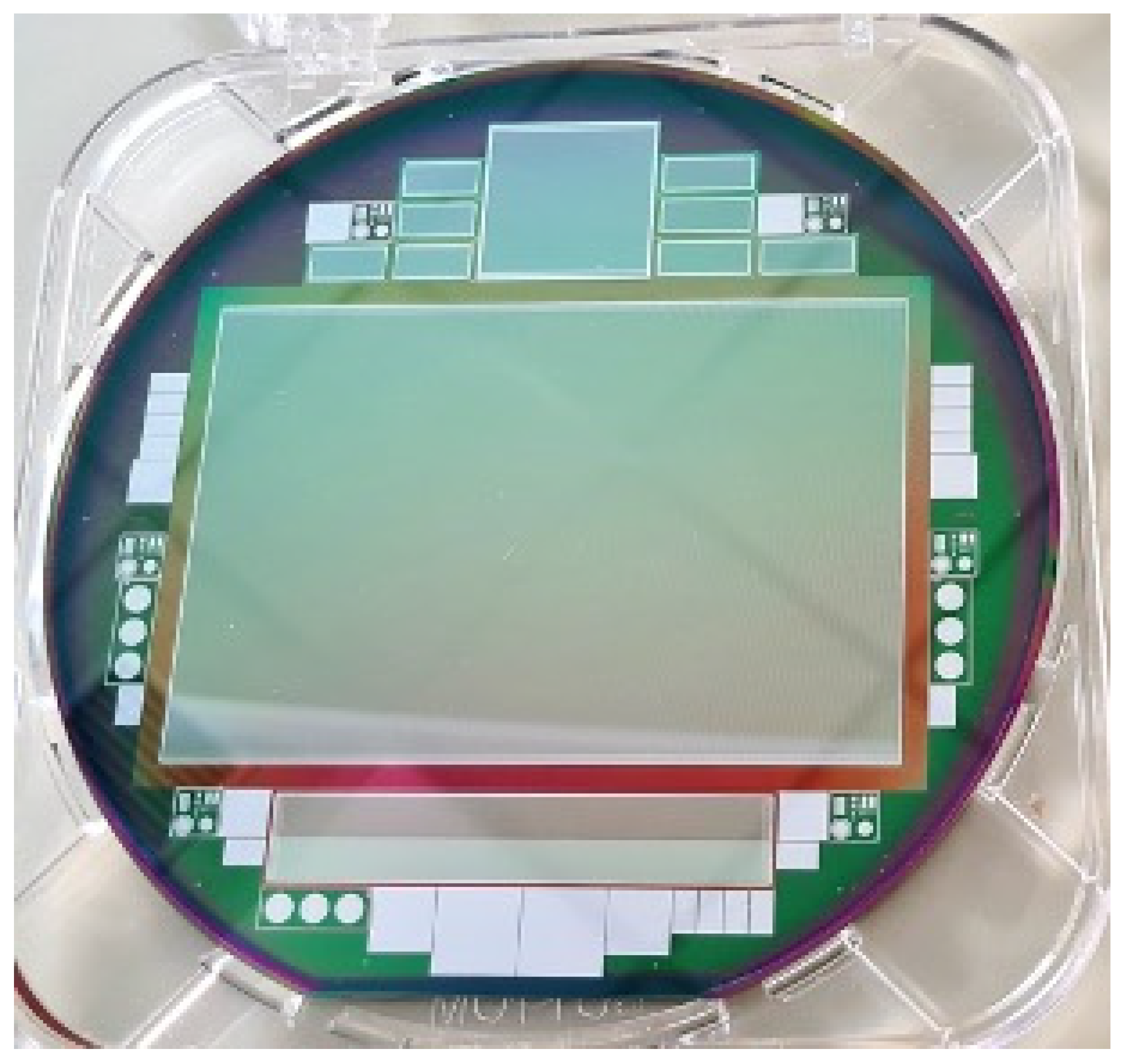
Figure 3.
Photograph of a 6-inch wafer processed at FBK (Trento, Italy) for double-sided strip detectors of LIMADOU HEPD-01 (courtesy of FBK). The main sensor at the center of the wafer has an overall size of ~10.6 × 7.1 cm2.
Figure 3.
Photograph of a 6-inch wafer processed at FBK (Trento, Italy) for double-sided strip detectors of LIMADOU HEPD-01 (courtesy of FBK). The main sensor at the center of the wafer has an overall size of ~10.6 × 7.1 cm2.

Figure 4.
Integrated passive components in microstrip detectors: poly-Si bias resistors and coupling capacitors.
Figure 4.
Integrated passive components in microstrip detectors: poly-Si bias resistors and coupling capacitors.

Figure 5.
Schematic cross-section of a double-sided microstrip detector (not to scale).

Figure 6.
Schematic cross-section of devices available in JSD technology from FBK (not to scale).

Figure 7.
Sketch of a DePFET.

Figure 8.
Schematic cross-section of a low-gain avalanche detector.

Figure 9.
Sketch of single-sided 3D detector process (not to scale): (a) wafer bonding; (b) p+ electrode definition and etching; (c) p+ electrode poly-Si filling and doping; (d) n+ electrode definition and etching; (e) n+ electrode poly-Si filling and doping; (f) contact opening, metal deposition and patterning.

Figure 10.
Sketch of 3D detector with active edge (not to scale).

Figure 11.
Schematic cross-section of a double-sided 3D detector (not to scale).

Figure 12.
Schematic cross-section of a single-sided 3D detector on Si-Si DWB substrates (not to scale).
Figure 12.
Schematic cross-section of a single-sided 3D detector on Si-Si DWB substrates (not to scale).

Figure 13.
Scanning electron microscope picture of the cross-section of a 3D-trench pixel detector made at FBK.
Figure 13.
Scanning electron microscope picture of the cross-section of a 3D-trench pixel detector made at FBK.

Disclaimer/Publisher’s Note: The statements, opinions and data contained in all publications are solely those of the individual author(s) and contributor(s) and not of MDPI and/or the editor(s). MDPI and/or the editor(s) disclaim responsibility for any injury to people or property resulting from any ideas, methods, instructions or products referred to in the content. |
© 2023 by the authors. Licensee MDPI, Basel, Switzerland. This article is an open access article distributed under the terms and conditions of the Creative Commons Attribution (CC BY) license (https://creativecommons.org/licenses/by/4.0/).
Share and Cite
MDPI and ACS Style
Dalla Betta, G.-F.; Ye, J. Silicon Radiation Detector Technologies: From Planar to 3D. Chips 2023, 2, 83-101. https://doi.org/10.3390/chips2020006
AMA Style
Dalla Betta G-F, Ye J. Silicon Radiation Detector Technologies: From Planar to 3D. Chips. 2023; 2(2):83-101. https://doi.org/10.3390/chips2020006
Chicago/Turabian StyleDalla Betta, Gian-Franco, and Jixing Ye. 2023. "Silicon Radiation Detector Technologies: From Planar to 3D" Chips 2, no. 2: 83-101. https://doi.org/10.3390/chips2020006