Low-Cost Indirect Measurements for Power-Efficient In-Field Optimization of Configurable Analog Front-Ends with Self-X Properties: A Hardware Implementation


Abstract
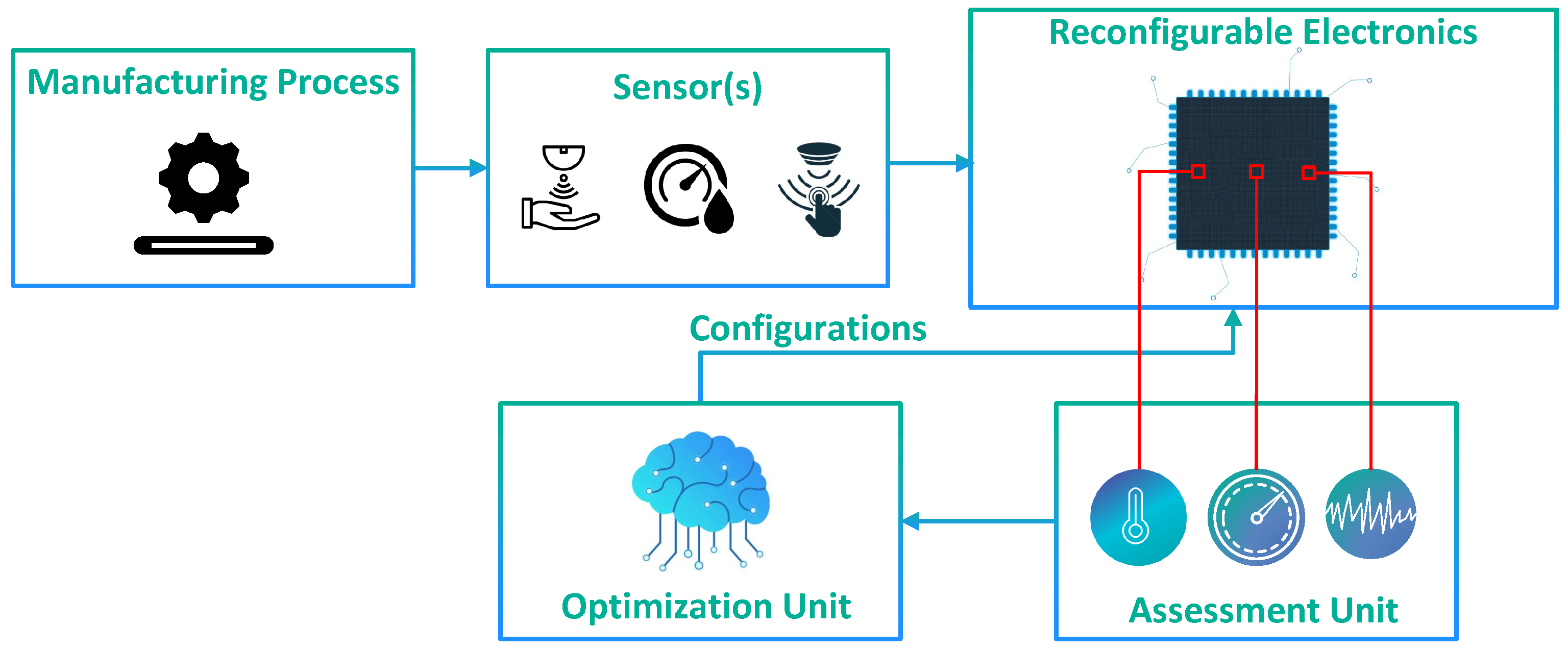
:1. Introduction
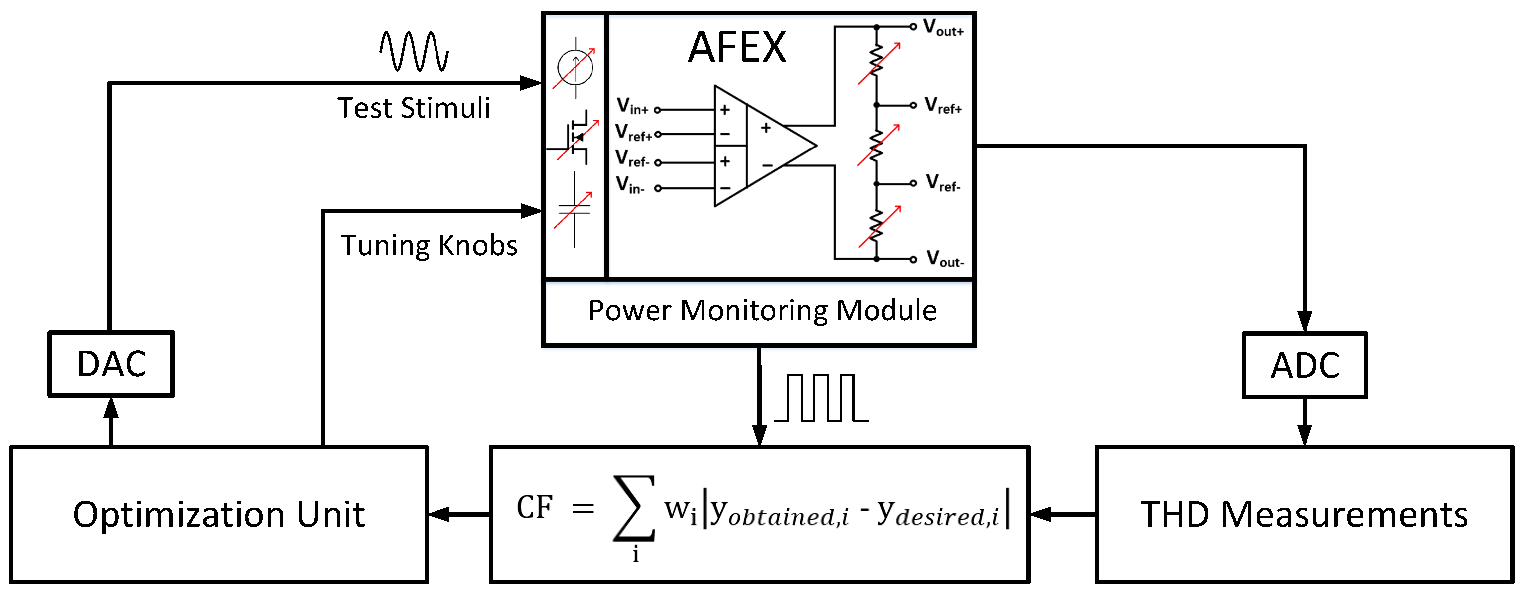
2. Proposed Methodology
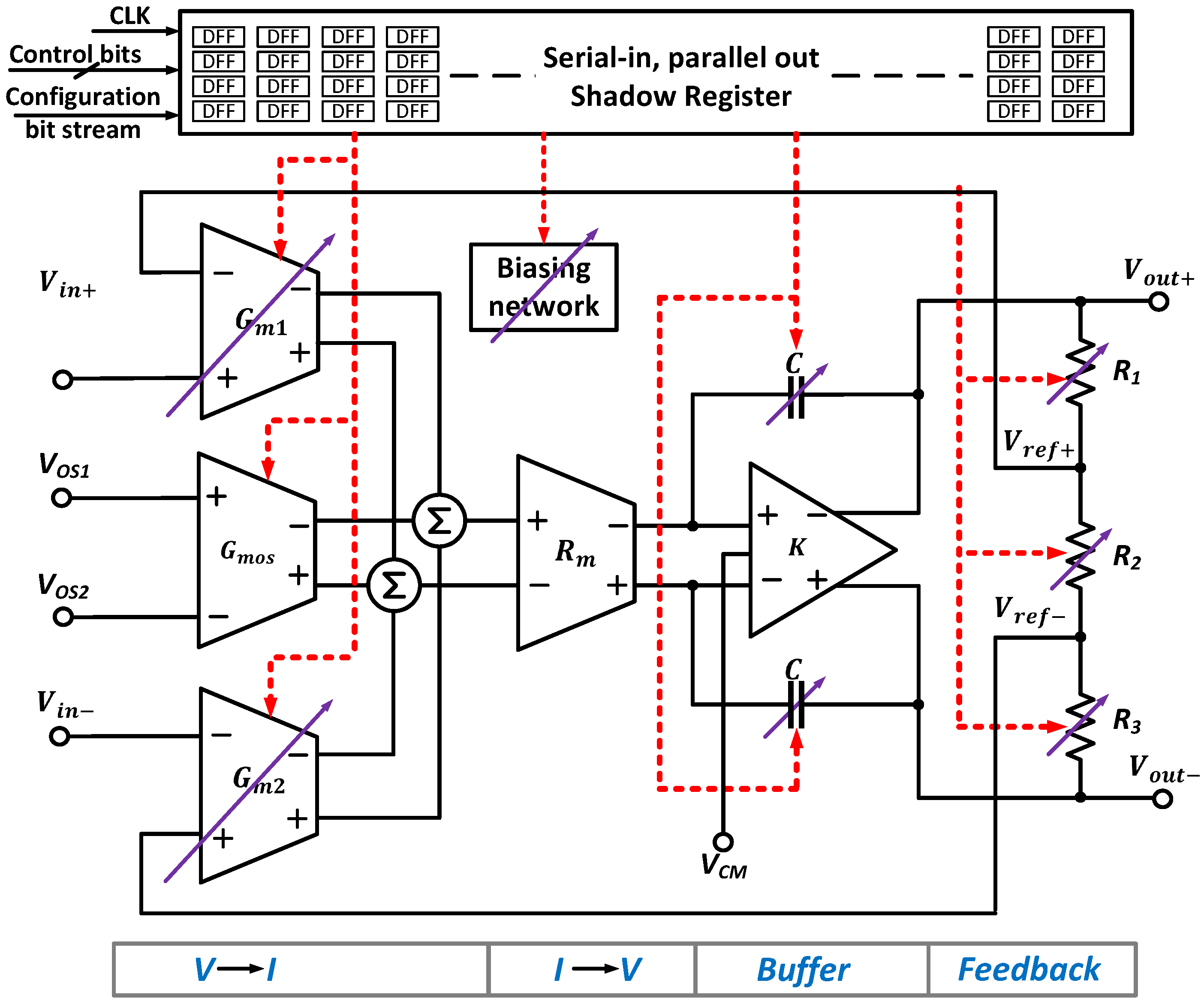
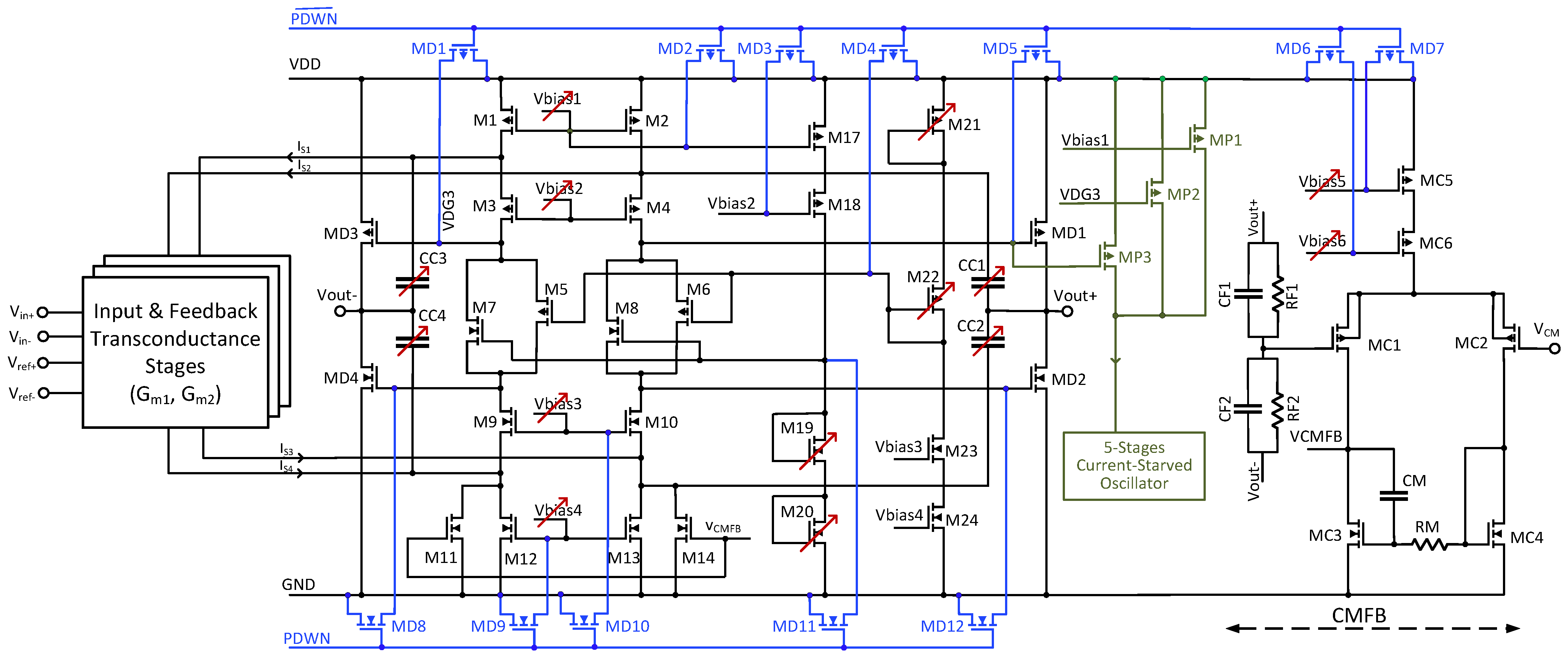
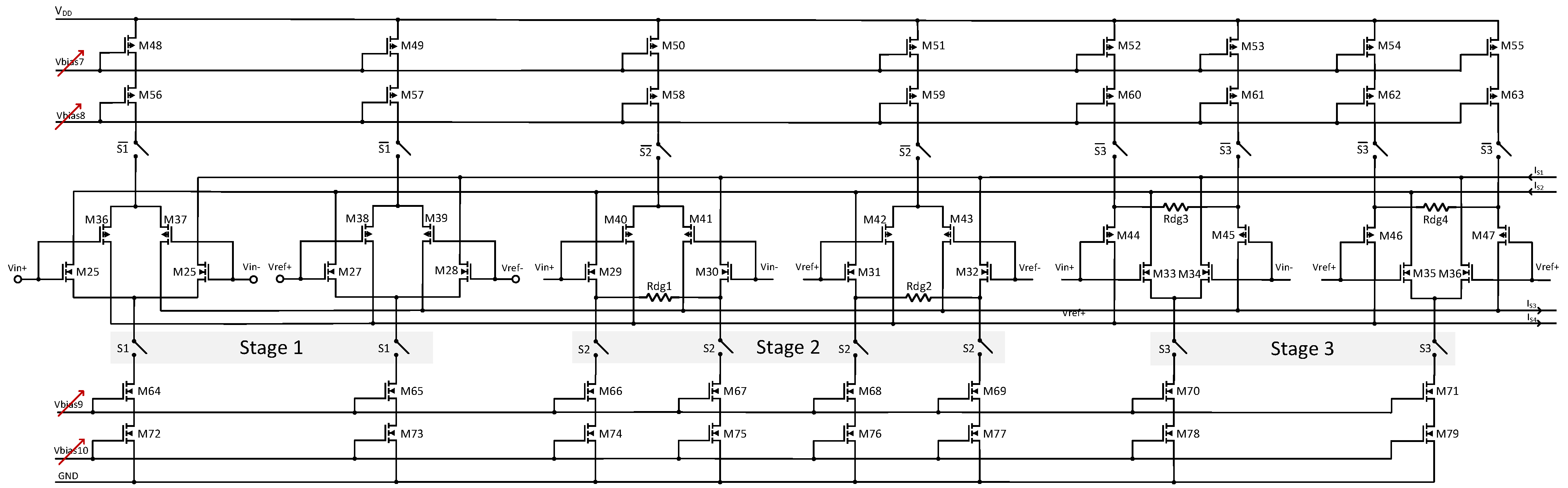
2.1. Indirect Current-Feedback Instrumentation Amplifier (CFIA)
2.2. Power Monitoring Module (PMM)
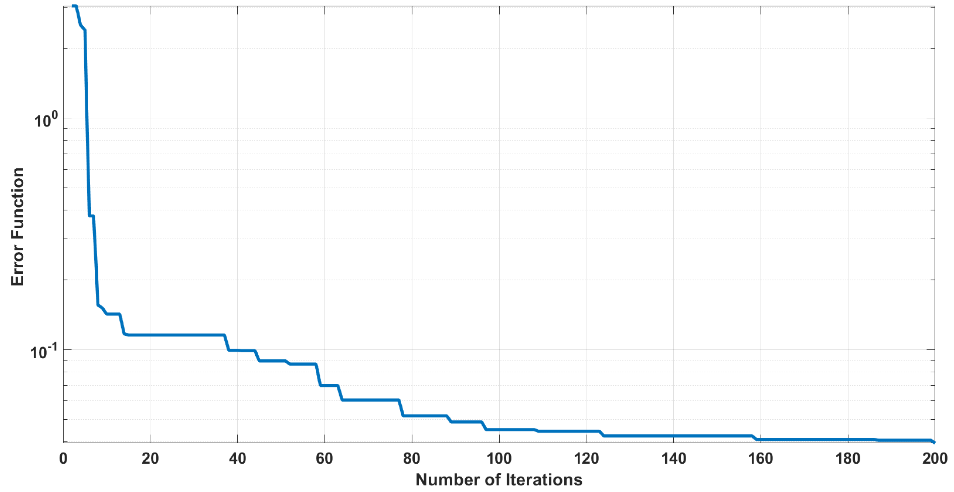
2.3. Experience Replay Particle Swarm Optimization (ERPSO)
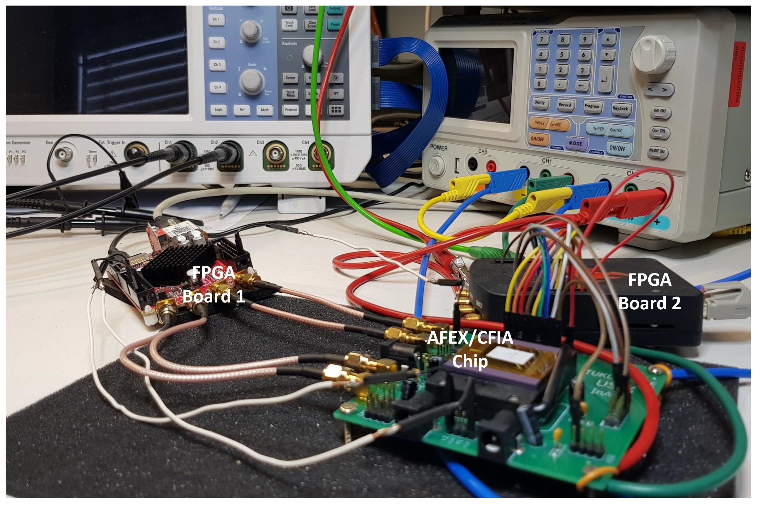
3. Experimental Setup
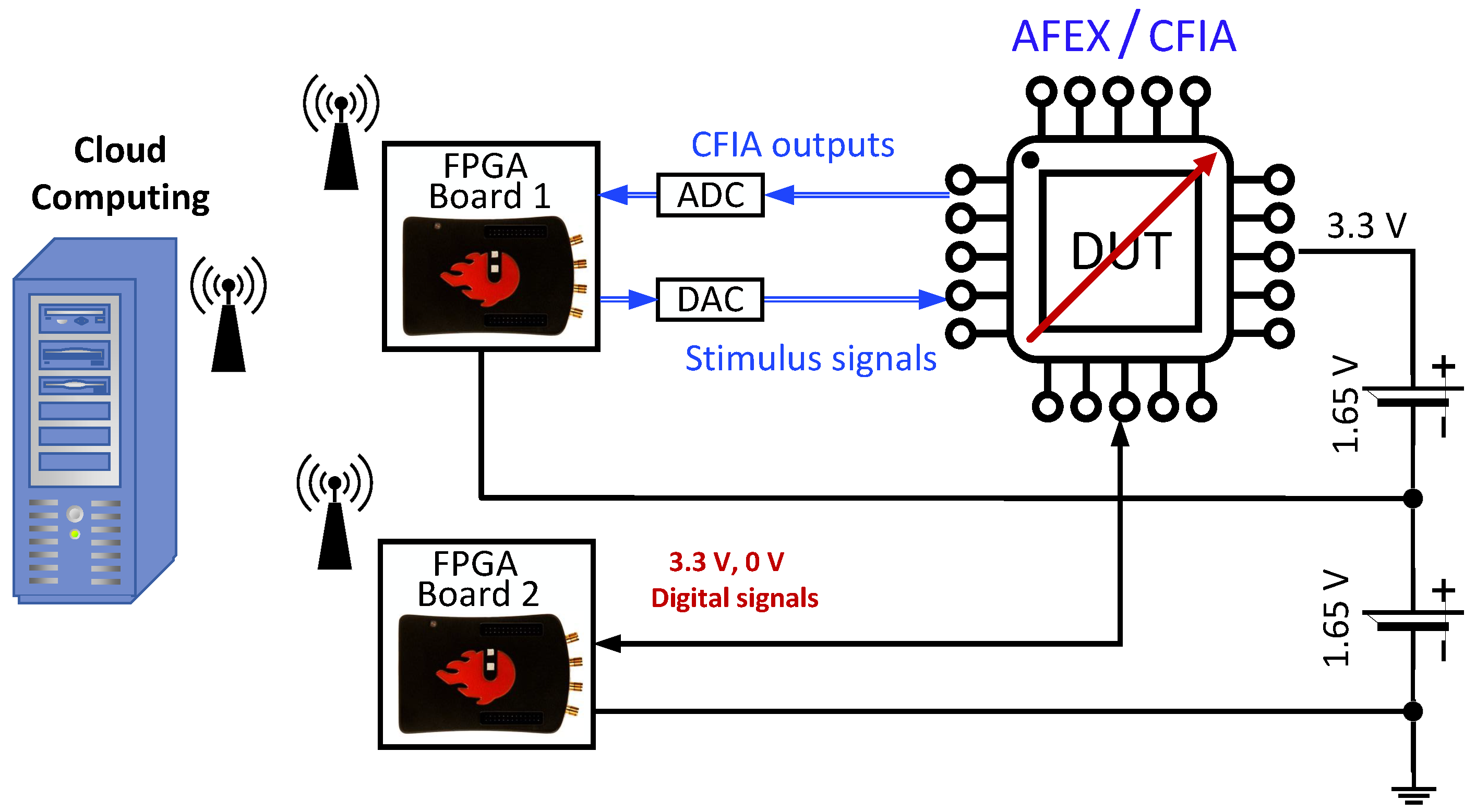
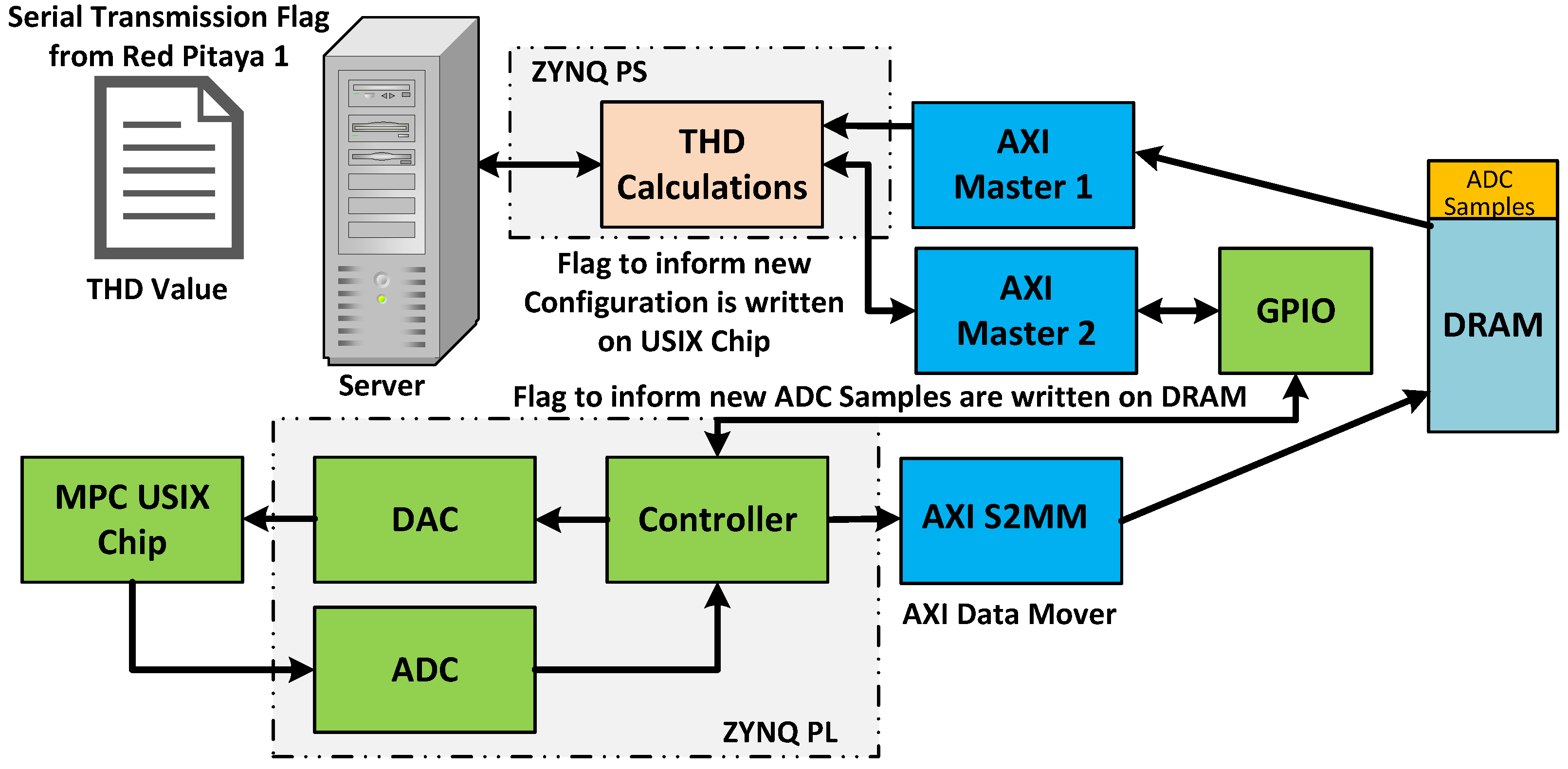
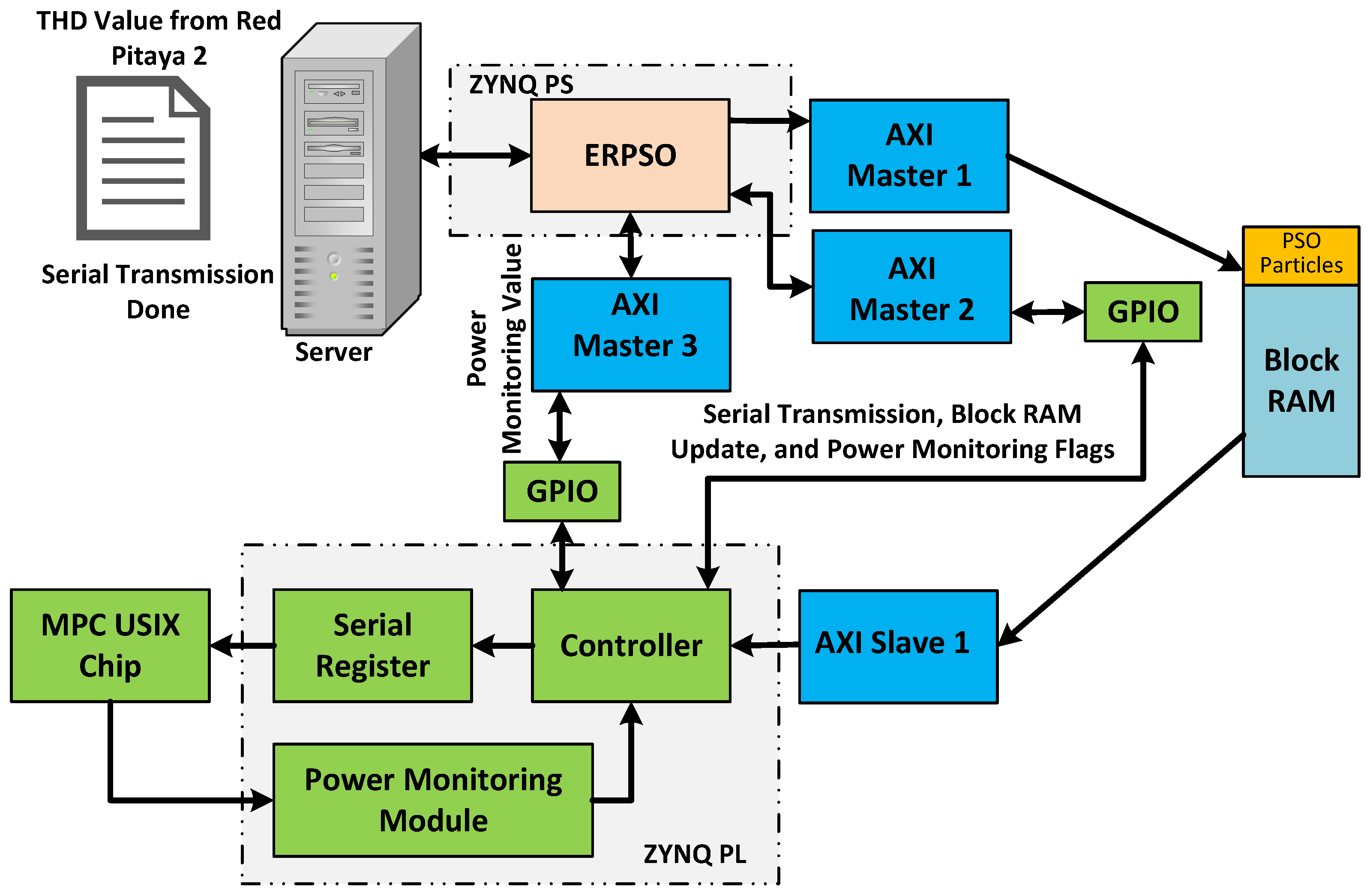
3.1. Intrinsic Implementation and Architecture of the Self-X System
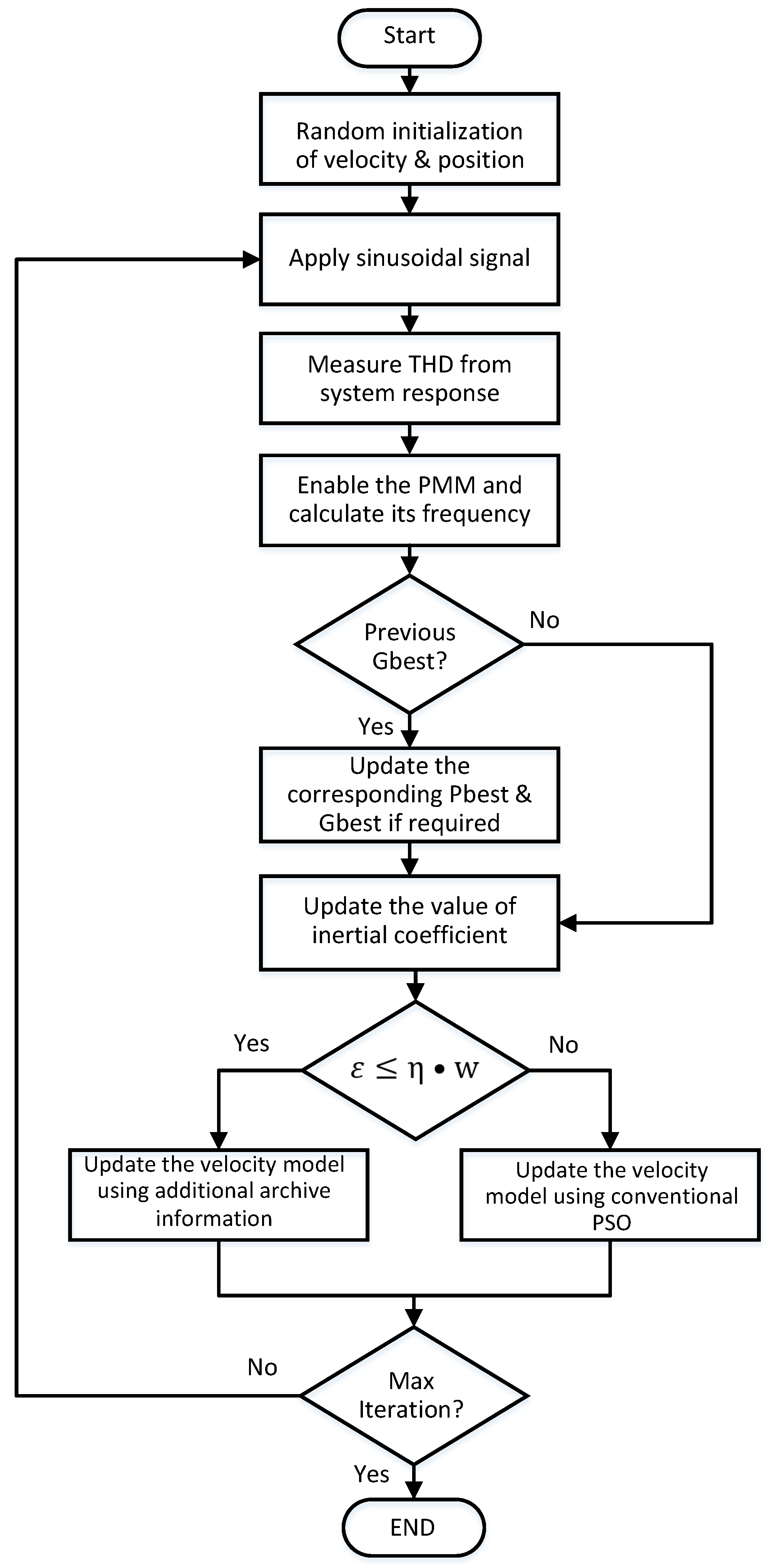
3.2. Workflow of the Optimization Process
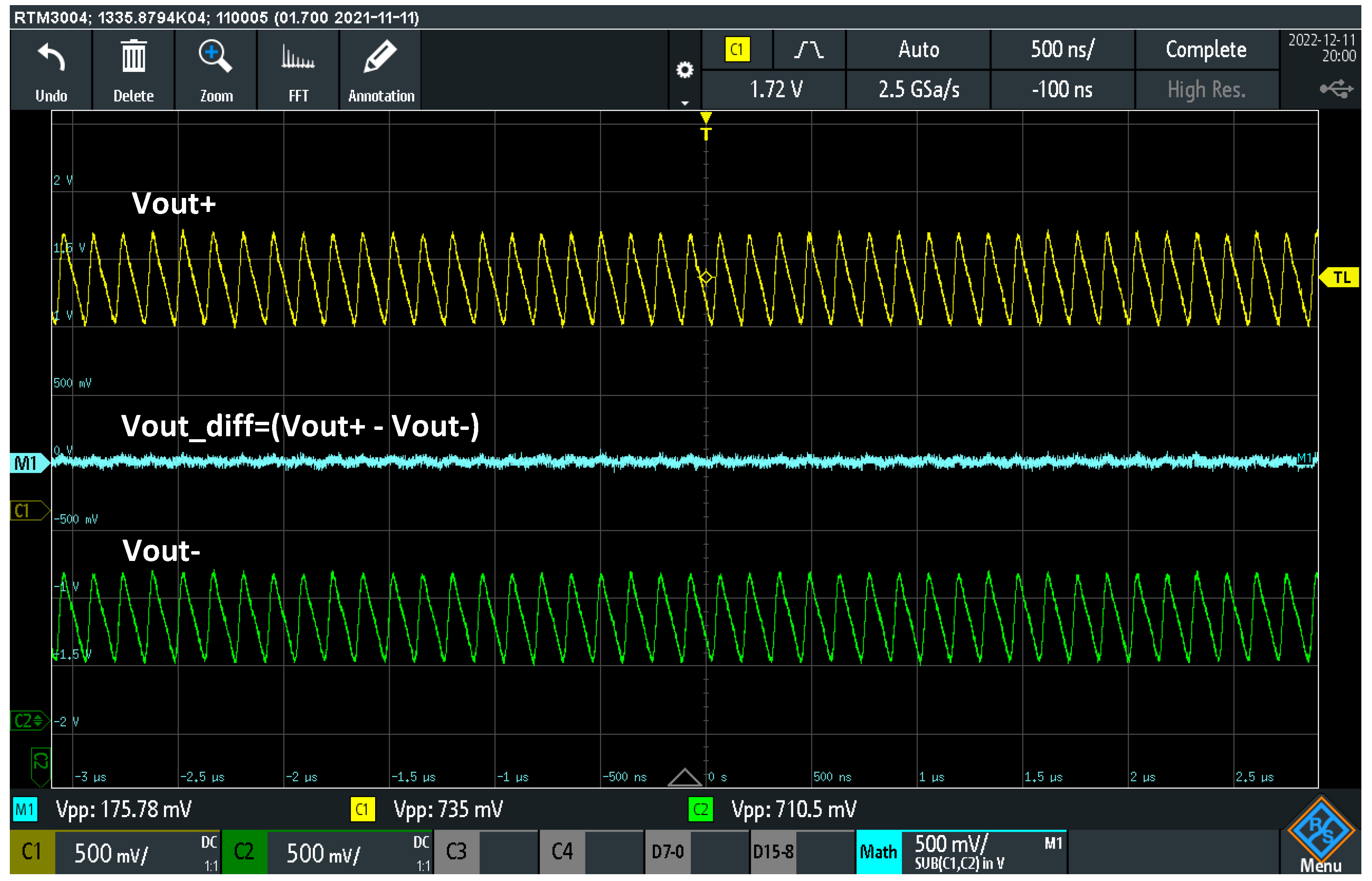
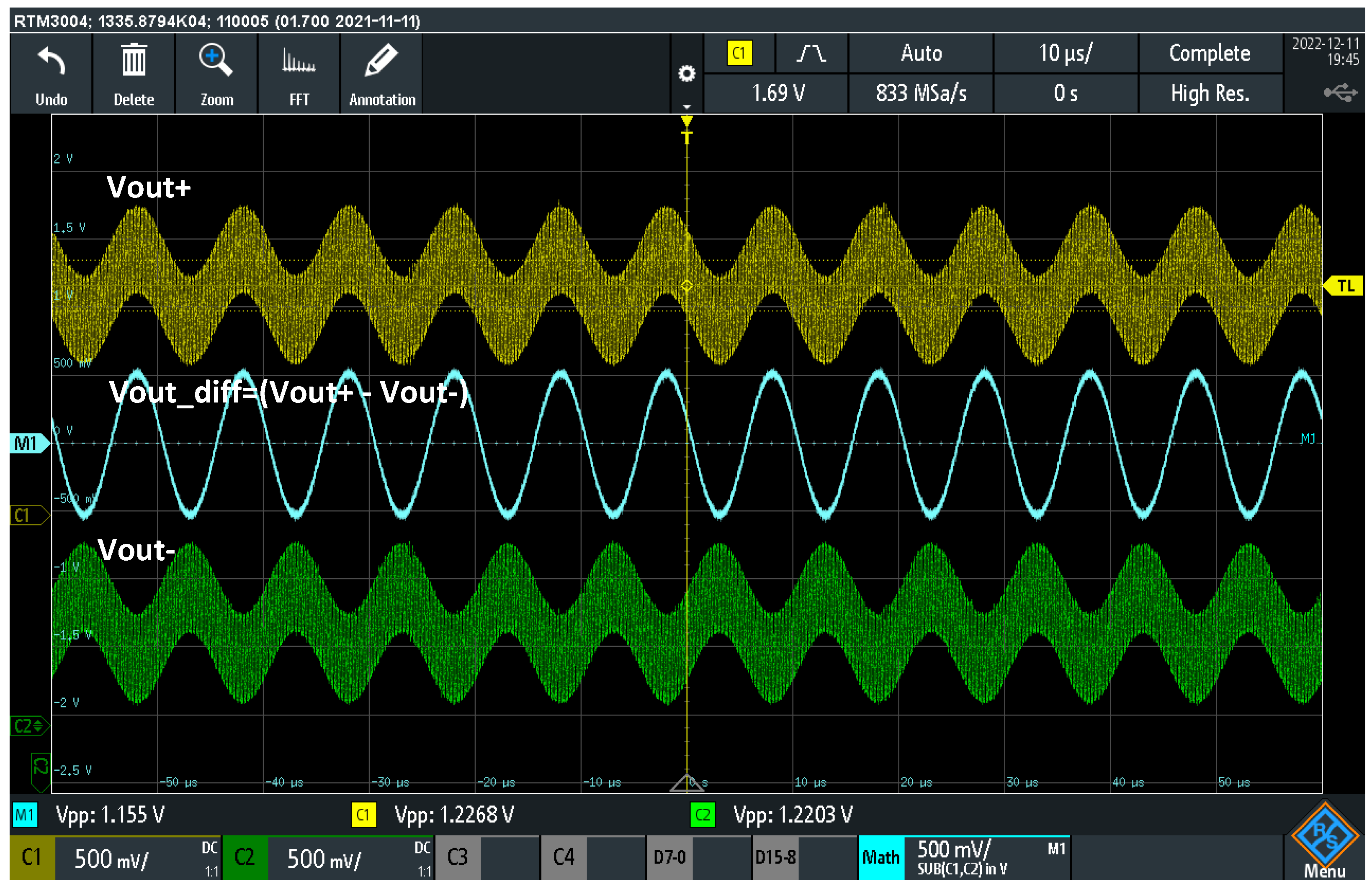
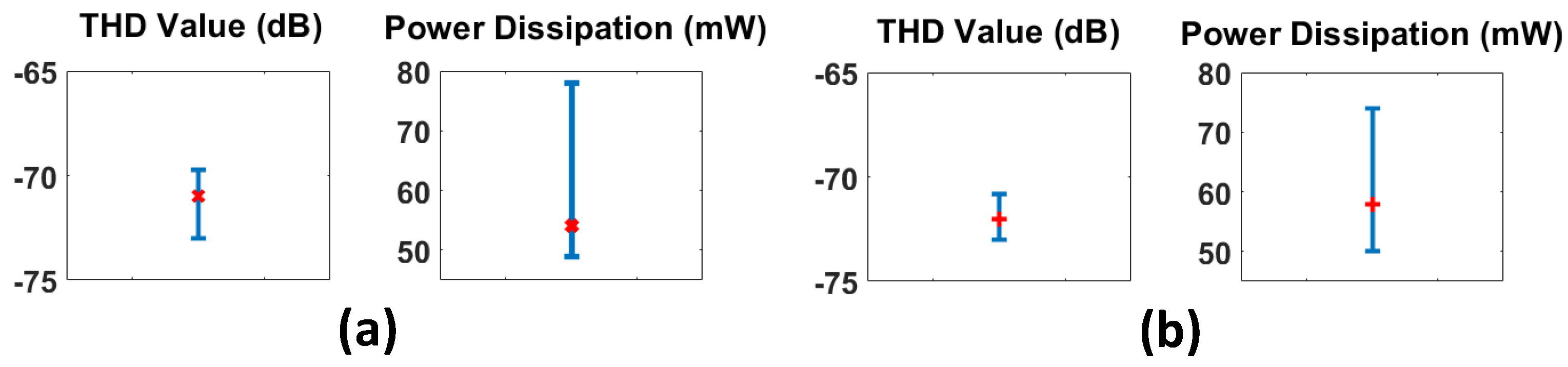
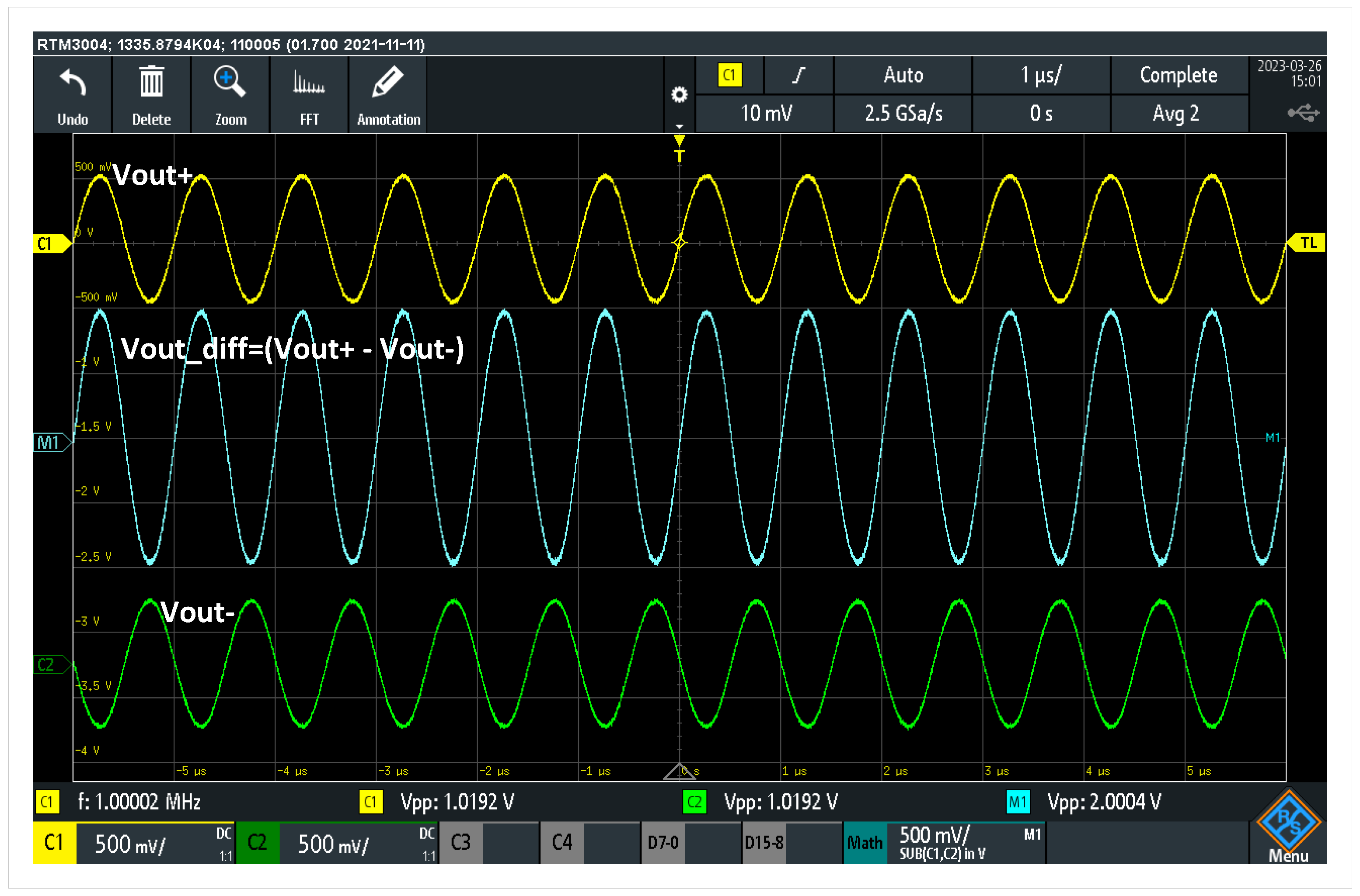
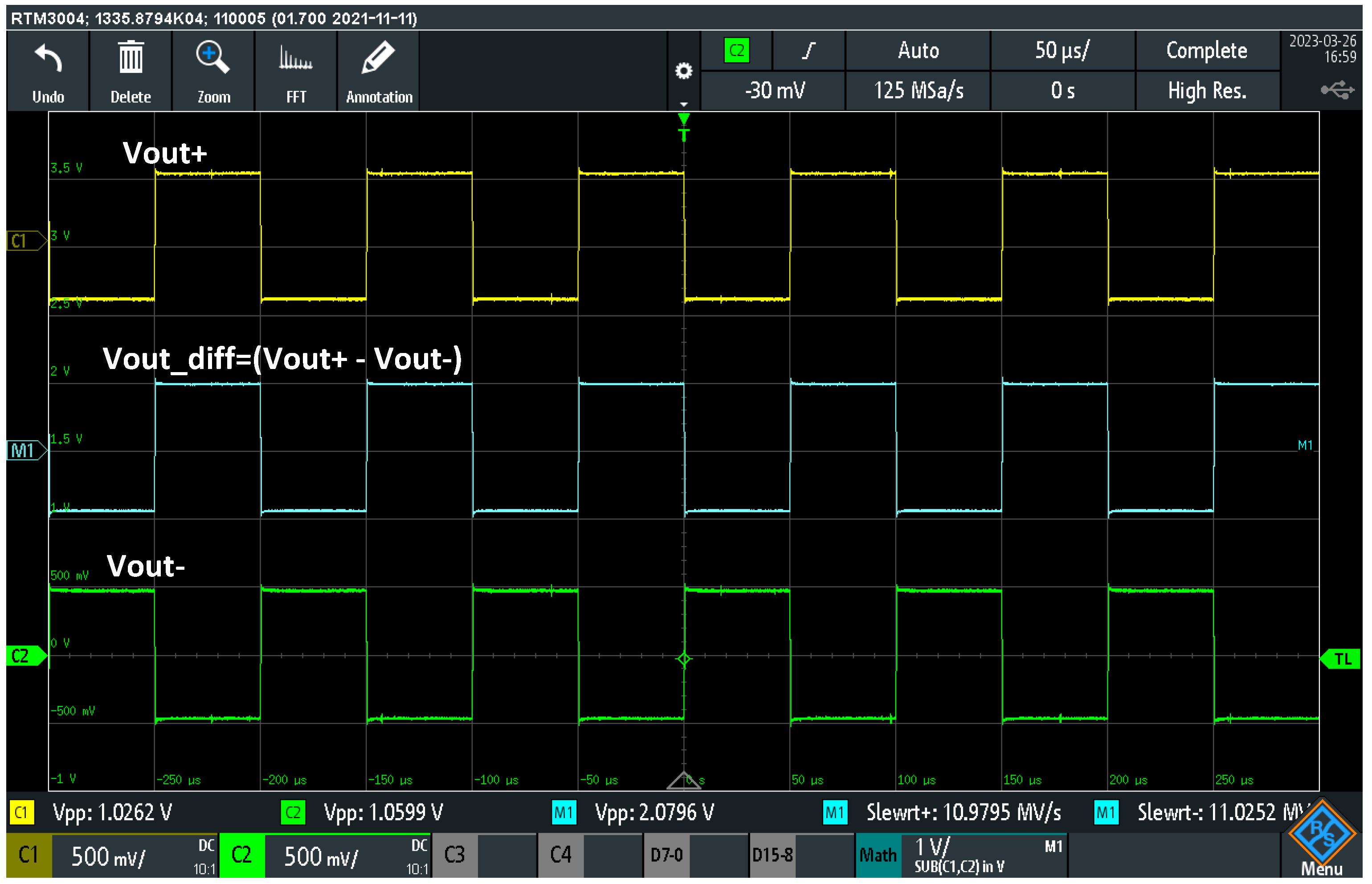
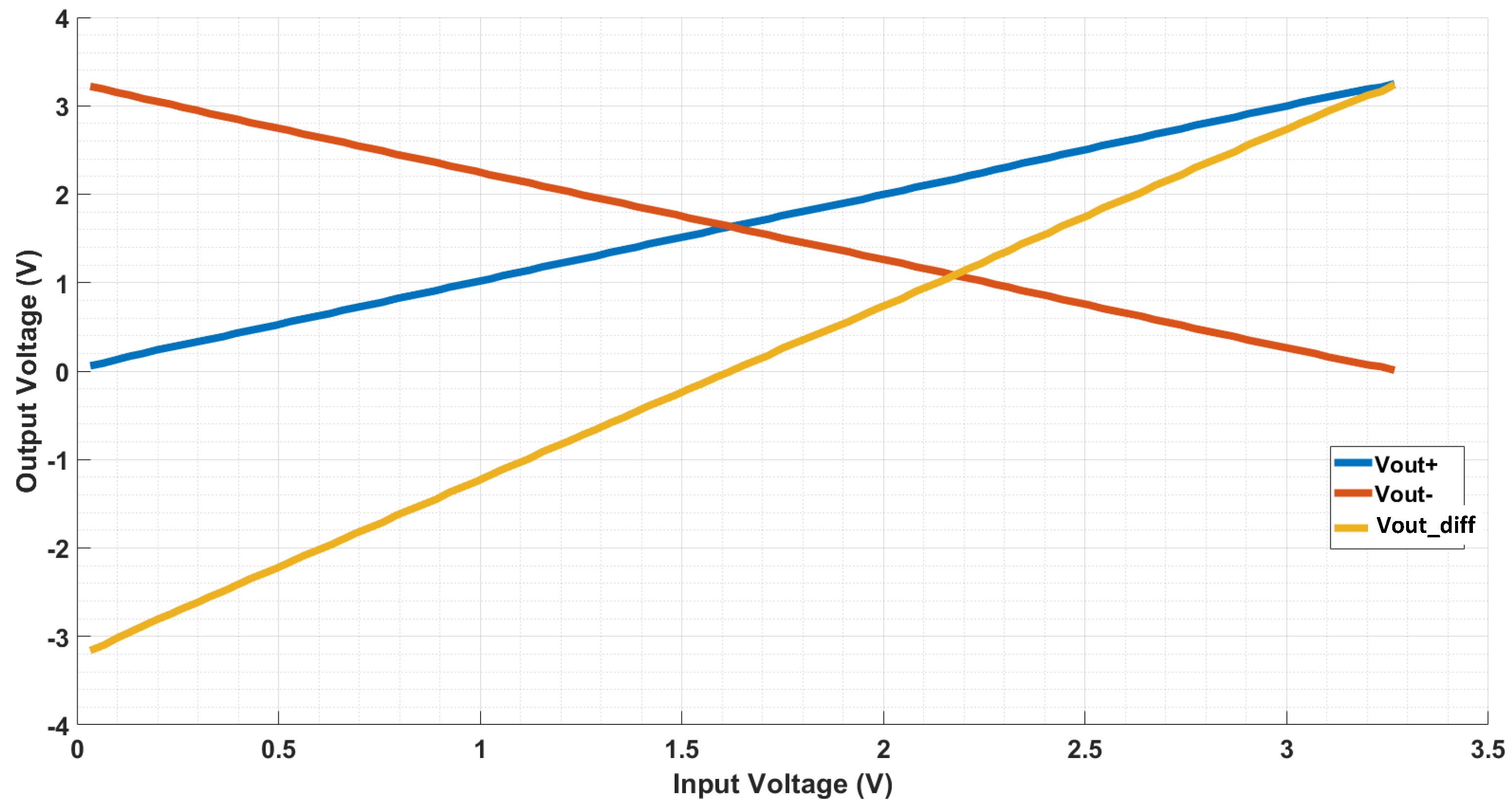
4. Measurement Results
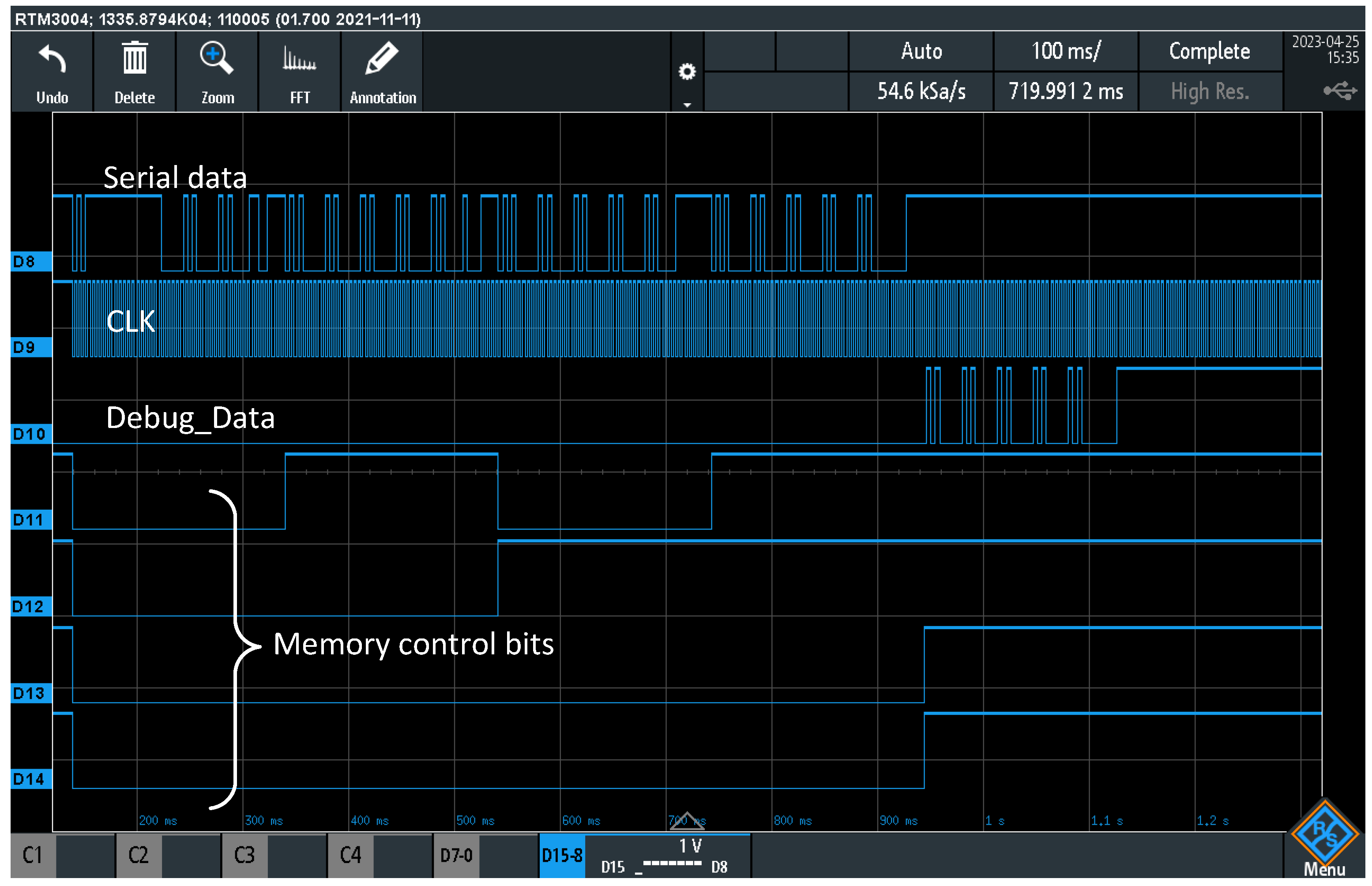
4.1. Shadow Register Verification
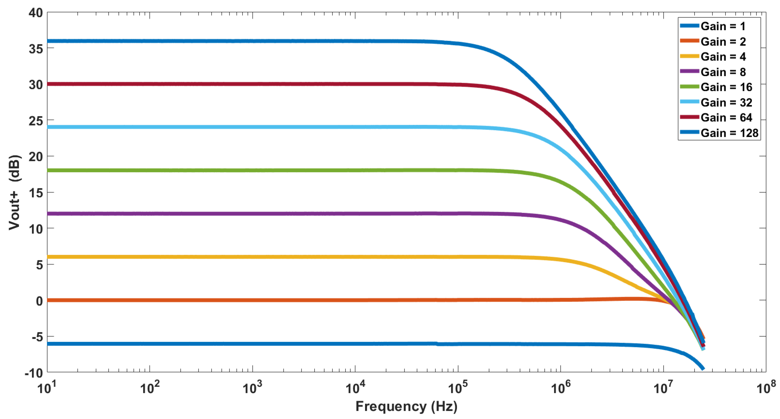
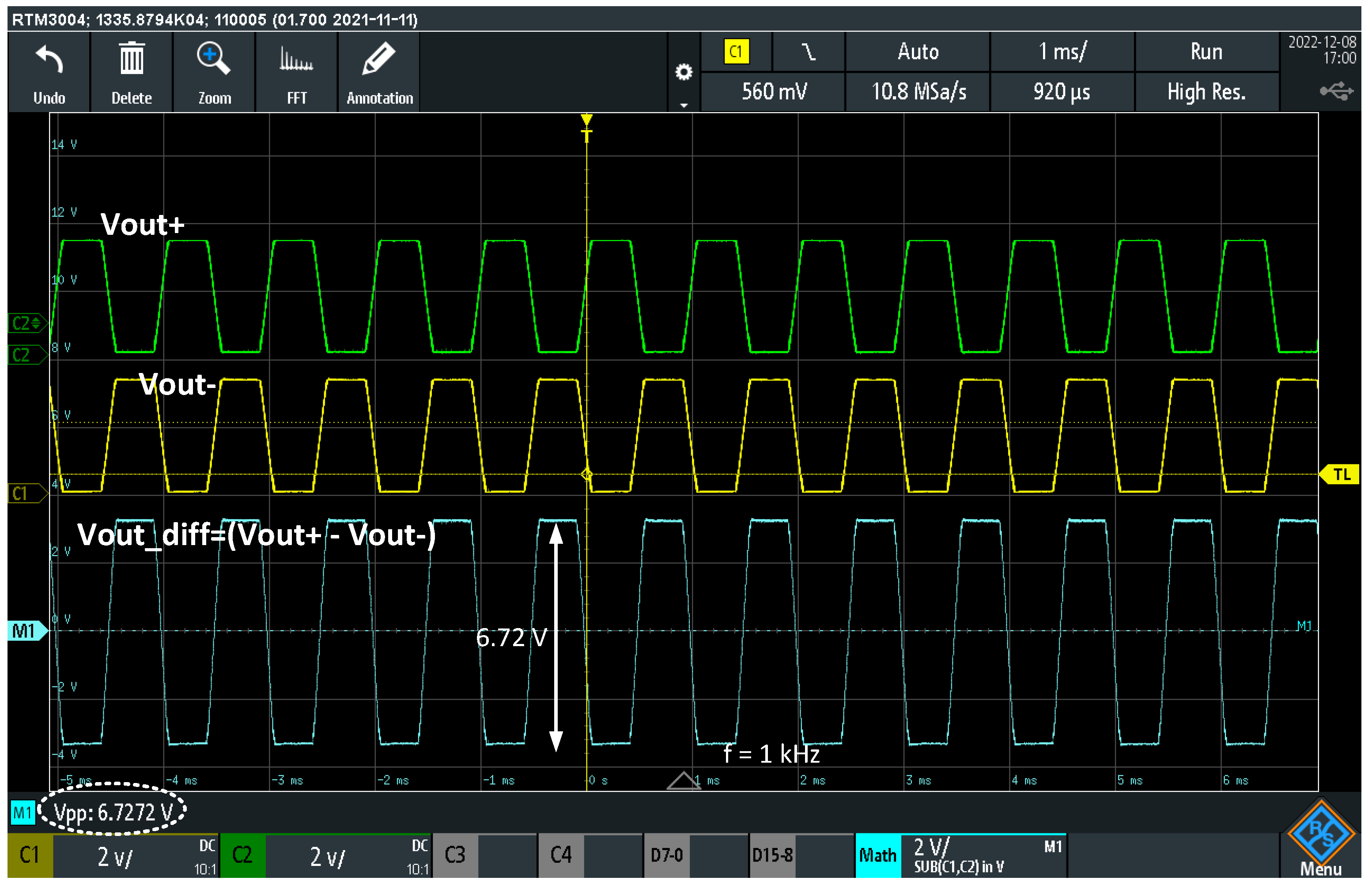
4.2. CFIA Testing Using the Default Configuration
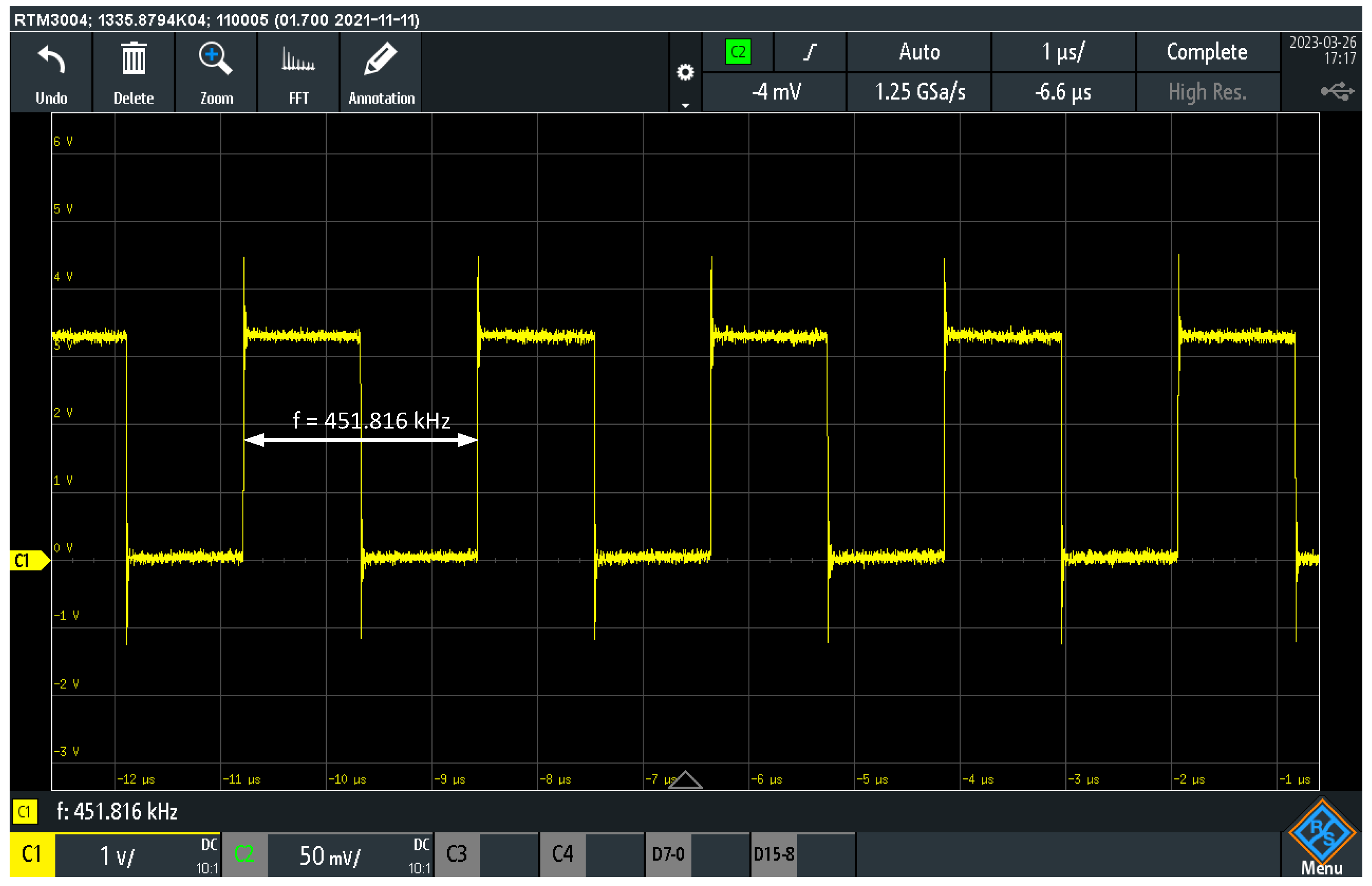
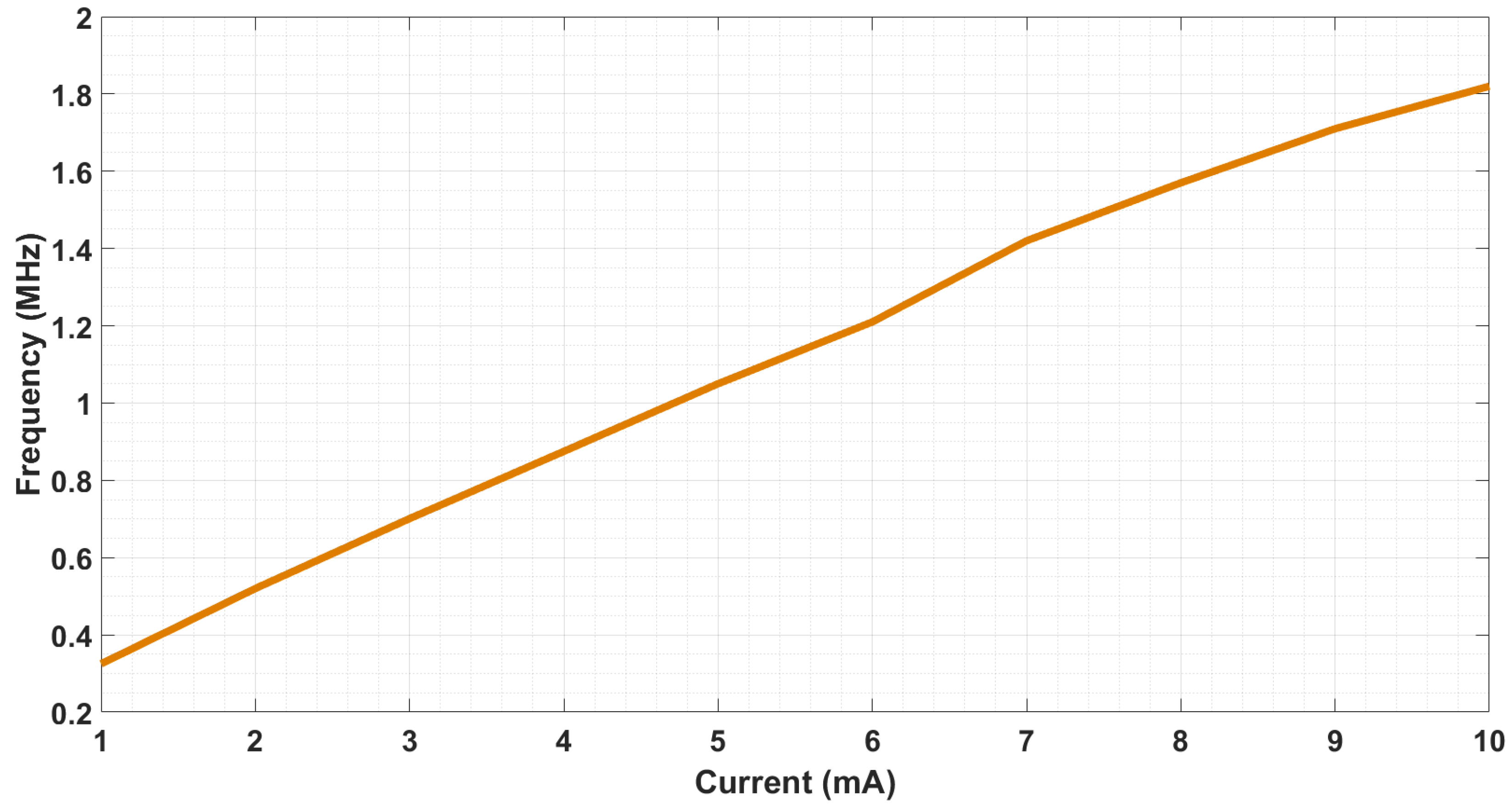
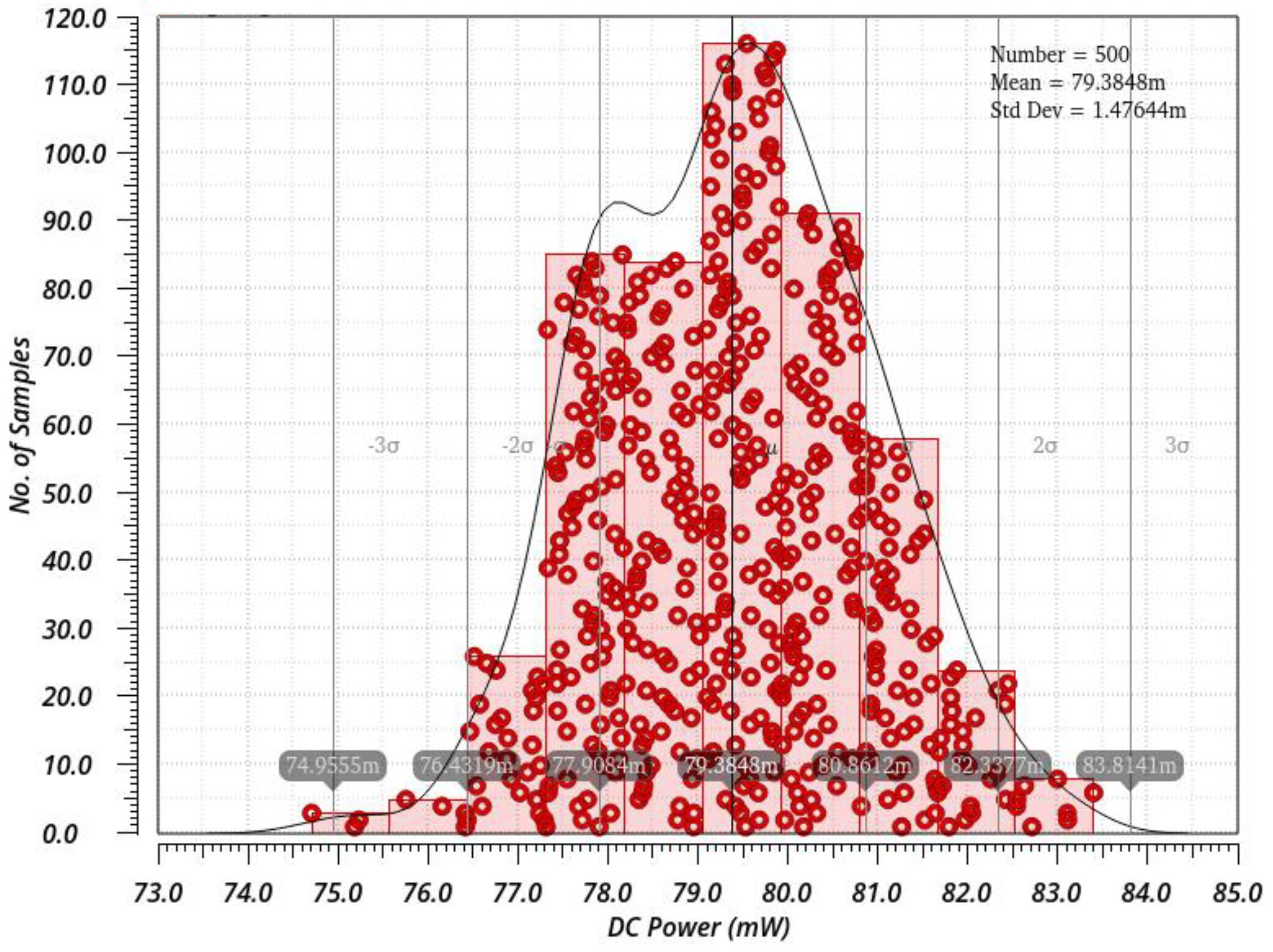
4.3. PMM Characterization
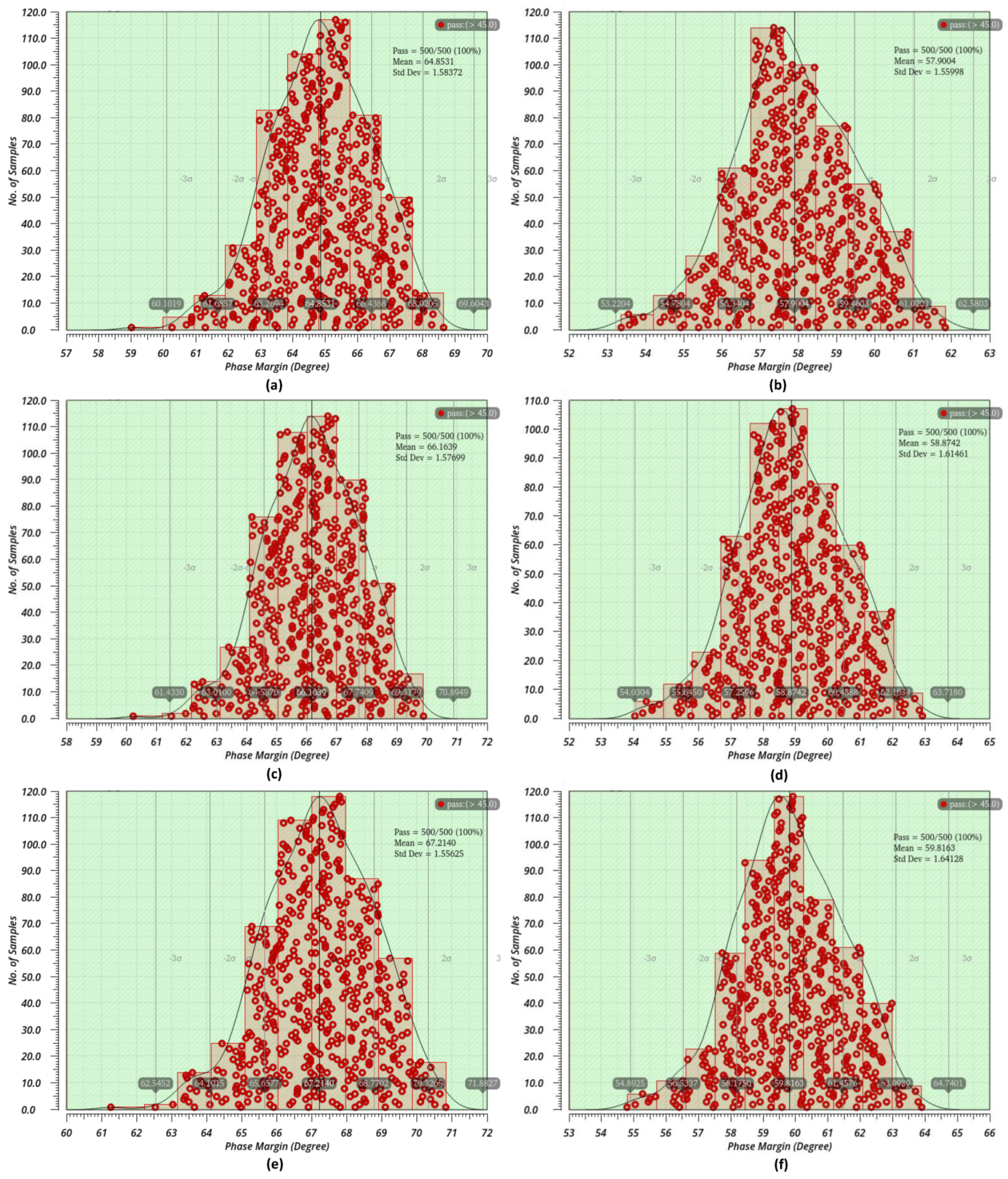
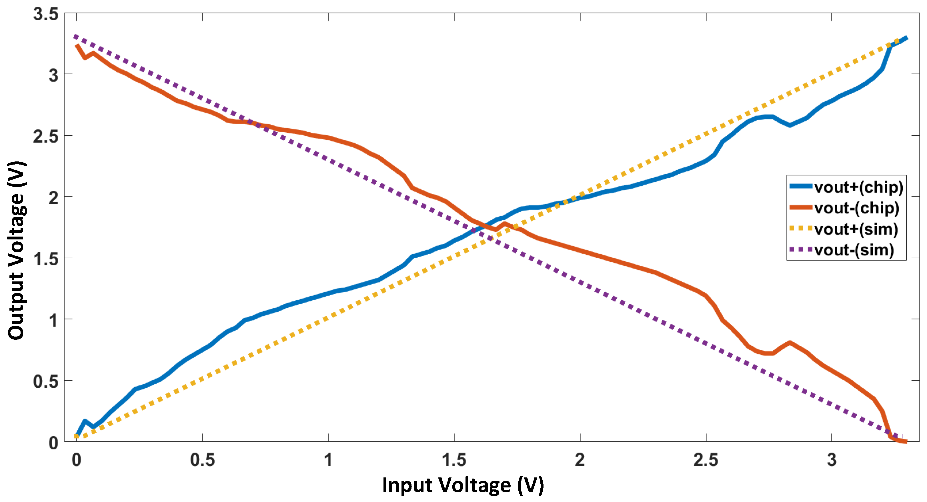
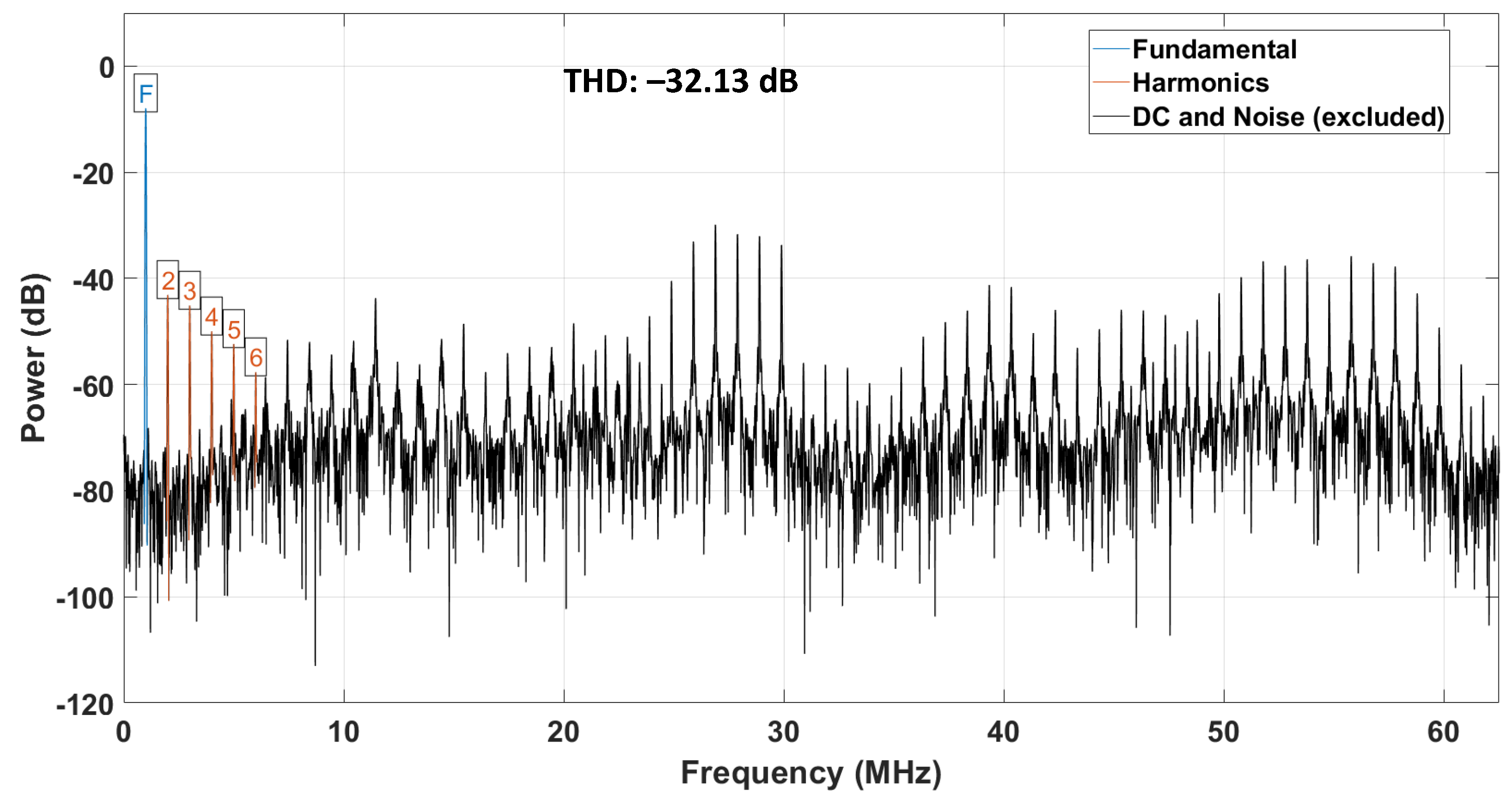
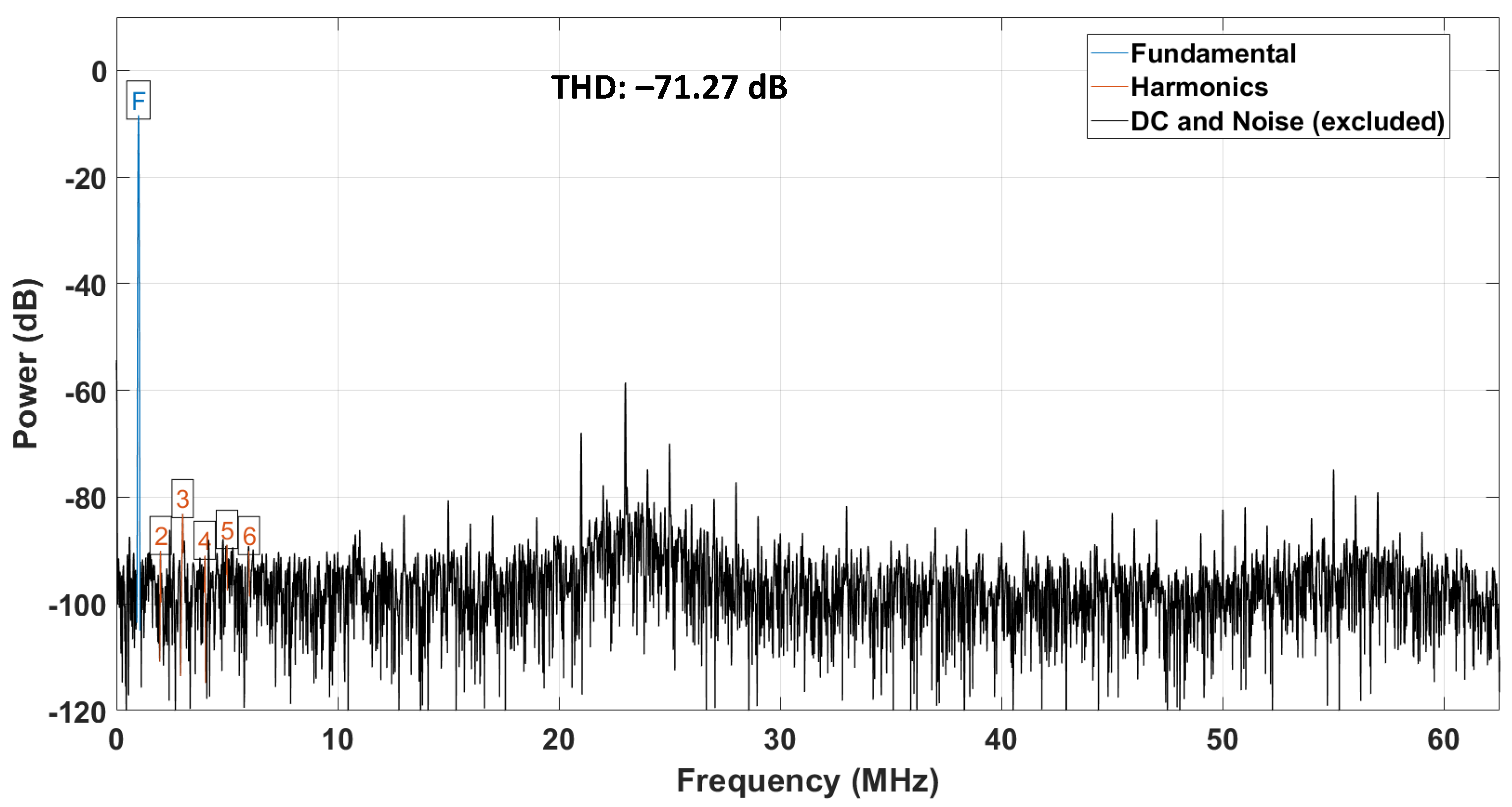
4.4. CFIA Performance Optimization Using the Proposed Methodology
5. Conclusions
Author Contributions
Funding
Institutional Review Board Statement
Informed Consent Statement
Data Availability Statement
Acknowledgments
Conflicts of Interest
Abbreviations
| CMOS | Complementary metal oxide semiconductor |
| AFE | Analog-front-ends |
| AFEX | Analog-front-ends with self-X properties |
| EHW | Evolvable hardware |
| PSO | Particle swarm optimization |
| ATE | Automatic test equipment |
| CFIA | Current-feedback in-amp |
| SIPO | Serial-in, parallel-out register |
| PMM | Power monitoring module |
| MHOAs | Meta-heuristic optimization algorithms |
| ERPSO | Experience replay particle swarm optimization |
| USIX | Universal sensor interface with self-X properties |
| ADC | Analog to digital converter |
| PM | Phase margin |
| GBW | Gain-bandwidth product |
| SR | Slew rate |
| THD | Total harmonic distortion |
| FFT | Fast Fourier Transform |
| FPGA | Field programmable gate array |
| SPI | Serial peripheral interface |
| DAC | Digital to analog converter |
References
- Diez-Olivan, A.; Del Ser, J.; Galar, D.; Sierra, B. Data fusion and machine learning for industrial prognosis: Trends and perspectives towards Industry 4.0. Inf. Fusion 2019, 50, 92–111. [Google Scholar] [CrossRef]
- Ahmed, I.; Jeon, G.; Piccialli, F. From artificial intelligence to explainable artificial intelligence in industry 4.0: A survey on what, how, and where. IEEE Trans. Ind. Inform. 2022, 18, 5031–5042. [Google Scholar] [CrossRef]
- Arrieta, A.B.; Díaz-Rodríguez, N.; Del Ser, J.; Bennetot, A.; Tabik, S.; Barbado, A.; García, S.; Gil-López, S.; Molina, D.; Benjamins, R.; et al. Explainable Artificial Intelligence (XAI): Concepts, taxonomies, opportunities and challenges toward responsible AI. Inf. Fusion 2020, 58, 82–115. [Google Scholar] [CrossRef]
- Kagermann, H.; Helbig, J.; Hellinger, A.; Wahlster, W. Recommendations for Implementing the Strategic Initiative INDUSTRIE 4.0: Securing the Future of German Manufacturing Industry; final report of the Industrie 4.0 Working Group; Forschungsunion, National Academy of Science and Engineering (acatech): Berlin, Germany, 2013. [Google Scholar]
- Wójcicki, K.; Biegańska, M.; Paliwoda, B.; Górna, J. Internet of Things in Industry: Research Profiling, Application, Challenges and Opportunities—A Review. Energies 2022, 15, 1806. [Google Scholar] [CrossRef]
- Trends, S. Trends in Future-Oriented Sensor Technologies; AMA Association for Sensor Technology: Berlin, Germany, 2014. [Google Scholar]
- Jamwal, A.; Agrawal, R.; Sharma, M.; Giallanza, A. Industry 4.0 technologies for manufacturing sustainability: A systematic review and future research directions. Appl. Sci. 2021, 11, 5725. [Google Scholar] [CrossRef]
- Lee, S.; Shi, C.; Wang, J.; Sanabria, A.; Osman, H.; Hu, J.; Sánchez-Sinencio, E. A built-in self-test and in situ analog circuit optimization platform. IEEE Trans. Circuits Syst. I Regul. Pap. 2018, 65, 3445–3458. [Google Scholar] [CrossRef]
- Lin, Y.B.; Lin, Y.W.; Lin, J.Y.; Hung, H.N. SensorTalk: An IoT device failure detection and calibration mechanism for smart farming. Sensors 2019, 19, 4788. [Google Scholar] [CrossRef]
- König, A. Integrated sensor electronics with self-x capabilities for advanced sensory systems as a baseline for industry 4.0. In Proceedings of the Sensors and Measuring Systems 19th ITG/GMA-Symposium, Nuremberg, Germany, 26–27 June 2018; pp. 1–4. [Google Scholar]
- White Paper on Industry 4.0, Join the Smart Revolution. Available online: https://www.displaytechnology.co.uk/assets/files/industry_4.0_white_paper.pdf (accessed on 19 April 2023).
- Chu, P.P. FPGA Prototyping by Verilog Examples: Xilinx Spartan-3 Version; John Wiley & Sons: Hoboken, NJ, USA, 2011. [Google Scholar]
- Kuhn, K.J.; Giles, M.D.; Becher, D.; Kolar, P.; Kornfeld, A.; Kotlyar, R.; Ma, S.T.; Maheshwari, A.; Mudanai, S. Process technology variation. IEEE Trans. Electron. Devices 2011, 58, 2197–2208. [Google Scholar] [CrossRef]
- Lewyn, L.L.; Ytterdal, T.; Wulff, C.; Martin, K. Analog circuit design in nanoscale CMOS technologies. Proc. IEEE 2009, 97, 1687–1714. [Google Scholar] [CrossRef]
- Hiblot, G.; Liu, Y.; Van der Plas, G. Impact of packaging stress on thinned 6T SRAM die. Int. J. Electron. Lett. 2020, 8, 38–45. [Google Scholar] [CrossRef]
- Semenov, O.; Vassighi, A.; Sachdev, M. Impact of self-heating effect on long-term reliability and performance degradation in CMOS circuits. IEEE Trans. Device Mater. Reliab. 2006, 6, 17–27. [Google Scholar] [CrossRef]
- Sapatnekar, S.S. What happens when circuits grow old: Aging issues in CMOS design. In Proceedings of the 2013 International Symposium on VLSI Technology, Systems and Application (VLSI-TSA). IEEE, Hsinchu, Taiwan, 22–24 April 2013; pp. 1–2. [Google Scholar]
- Yellepeddi, M.; Kelkar, A.; Waldrip, J. Analog Circuit Design Strategies for Reliability Tolerance: Planning for Reliability Effects While Designing Circuits in Modern CMOS Technologies. IEEE Solid-State Circuits Mag. 2020, 12, 79–85. [Google Scholar] [CrossRef]
- Schaldenbrand, A. Analog Reliability Analysis for Mission-Critical Applications; White Paper; Cadence Design Systems, Inc.: San Jose, CA, USA, 2019. [Google Scholar]
- Li, X.; Taylor, B.; Chien, Y.; Pileggi, L.T. Adaptive post-silicon tuning for analog circuits: Concept, analysis and optimization. In Proceedings of the 2007 IEEE/ACM International Conference on Computer-Aided Design, IEEE, San Jose, CA, USA, 4–8 November 2007; pp. 450–457. [Google Scholar]
- Du, D.; Odame, K.M. A bandwidth-adaptive preamplifier. IEEE J. Solid-State Circuits 2013, 48, 2142–2153. [Google Scholar]
- Huang, Y.J.; Tzeng, T.H.; Lin, T.W.; Huang, C.W.; Yen, P.W.; Kuo, P.H.; Lin, C.T.; Lu, S.S. A self-powered CMOS reconfigurable multi-sensor SoC for biomedical applications. IEEE J. Solid-State Circuits 2014, 49, 851–866. [Google Scholar] [CrossRef]
- Thompson, A. An evolved circuit, intrinsic in silicon, entwined with physics. In Proceedings of the Evolvable Systems: From Biology to Hardware: First International Conference, ICES96 Tsukuba, Japan, 7–8 October 1996; Proceedings 1. pp. 390–405. [Google Scholar]
- Abd, H.; König, A. Design of a CMOS memristor emulator-based, self-adaptive spiking analog-to-digital data conversion as the lowest level of a self-x hierarchy. J. Sensors Sens. Syst. 2022, 11, 233–262. [Google Scholar] [CrossRef]
- Tawdross, P.; Konig, A. Investigation of particle swarm optimization for dynamic reconfiguration of field-programmable analog circuits. In Proceedings of the Fifth International Conference on Hybrid Intelligent Systems (HIS’05), Rio de Janeiro, Brazil, 6–9 November 2005; p. 6. [Google Scholar]
- Shang, Q.; Chen, L.; Wang, D.; Tong, R.; Peng, P. Evolvable hardware design of digital circuits based on adaptive genetic algorithm. In Proceedings of the International Conference on Applications and Techniques in Cyber Intelligence ATCI 2019: Applications and Techniques in Cyber Intelligence 7, Huainan, China, 22–24 June 2019; pp. 791–800. [Google Scholar]
- Ramesham, R.; Kumar, N.; Mao, J.; Keymeulen, D.; Zebulum, R.S.; Stoica, A. Data converters performance at extreme temperatures. In Proceedings of the 2006 IEEE Aerospace Conference. IEEE, Big Sky, MT, USA, 4–11 March 2006; p. 12. [Google Scholar]
- Andraud, M.; Stratigopoulos, H.G.; Simeu, E. One-shot non-intrusive calibration against process variations for analog/rf circuits. IEEE Trans. Circuits Syst. I Regul. Pap. 2016, 63, 2022–2035. [Google Scholar] [CrossRef]
- In-Chip Monitoring and Sensing. Available online: https://www.synopsys.com/solutions/silicon-lifecycle-management/in-chip-monitoring-and-sensing.html (accessed on 19 May 2022).
- Kashyap, R. Silicon lifecycle management (SLM) with in-chip monitoring. In Proceedings of the 2021 IEEE International Reliability Physics Symposium (IRPS), Monterey, CA, USA, 21–25 March 2021; pp. 1–4. [Google Scholar] [CrossRef]
- Silicon Lifecycle Management: Actionable Silicon Insights Through Intelligent Measurement and Analysis. Available online: https://www.synopsys.com/solutions/silicon-lifecycle-management.html (accessed on 19 May 2022).
- Synopsys Expansion of Silicon Lifecycle Management Platform. Available online: https://www.eetasia.com/synopsys-acquires-moortec-to-expand-silicon-lifecycle-management-platform/ (accessed on 19 May 2022).
- Variyam, P.N.; Cherubal, S.; Chatterjee, A. Prediction of analog performance parameters using fast transient testing. IEEE Trans. Comput.-Aided Des. Integr. Circuits Syst. 2002, 21, 349–361. [Google Scholar] [CrossRef]
- Stratigopoulos, H.G.; Mir, S. Adaptive alternate analog test. IEEE Des. Test Comput. 2012, 29, 71–79. [Google Scholar] [CrossRef]
- Andraud, M.; Verhelst, M. From on-chip self-healing to self-adaptivity in analog/RF ICs: Challenges and opportunities. In Proceedings of the 2018 IEEE 24th International Symposium on On-Line Testing And Robust System Design (IOLTS), Platja d’Aro, Spain, 2–4 July 2018; pp. 131–134. [Google Scholar]
- Alraho, S.; Zaman, Q.; Abd, H.; König, A. Integrated Sensor Electronic Front-Ends with Self-X Capabilities. Chips 2022, 1, 83–120. [Google Scholar] [CrossRef]
- Zaman, Q.; Alraho, S.; König, A. Efficient transient testing procedure using a novel experience replay particle swarm optimizer for THD-based robust design and optimization of self-X sensory electronics in industry 4.0. J. Sensors Sens. Syst. 2021, 10, 193–206. [Google Scholar] [CrossRef]
- Red Pitaya Doumentation. Available online: https://redpitaya.com/documentation/ (accessed on 23 April 2022).
- Stoica, A. Toward evolvable hardware chips: Experiments with a programmable transistor array. In Proceedings of the Seventh International Conference on Microelectronics for Neural, Fuzzy and Bio-Inspired Systems, Granada, Spain, 9 April 1999; pp. 156–162. [Google Scholar] [CrossRef]
- Tawdross, P.M.M. Bio-Inspired Circuit Sizing and Trimming Methods for Dynamically Reconfigurable Sensor Electronics in Industrial Embedded Systems. Doctoral Thesis, Technische Universität Kaiserslautern, Kaiserslautern, Germany, 2007. [Google Scholar]
- Wu, R.; Huijsing, J.H.; Makinwa, K.A. Precision Instrumentation Amplifiers and Read-Out Integrated Circuits; Springer Science & Business Media: Berlin/Heidelberg, Germany, 2012. [Google Scholar]
- Han, K.; Kim, H.; Kim, J.; You, D.; Heo, H.; Kwon, Y.; Lee, J.; Ko, H. A 24.88 nV/Hz Wheatstone Bridge Readout Integrated Circuit with Chopper-Stabilized Multipath Operational Amplifier. Appl. Sci. 2020, 10, 399. [Google Scholar] [CrossRef]
- Fan, Q.; Makinwa, K.A.; Huijsing, J.H. Capacitively Coupled Chopper Instrumentation Amplifiers for Low-Voltage Applications. In Capacitively-Coupled Chopper Amplifiers; Springer: Berlin/Heidelberg, Germany, 2017; pp. 93–121. [Google Scholar]
- Corbacho, I.; Carrillo, J.M.; Ausín, J.L.; Domínguez, M.Á.; Pérez-Aloe, R.; Duque-Carrillo, J.F. A Fully-Differential CMOS Instrumentation Amplifier for Bioimpedance-Based IoT Medical Devices. J. Low Power Electron. Appl. 2022, 13, 3. [Google Scholar] [CrossRef]
- Brunner, E.; Gilbert, B. The active feedback amplifier. a versatile analog building block. In Proceedings of the NORTHCON’94, Seattle, WA, USA, 13 October 1994; pp. 131–136. [Google Scholar]
- Sackinger, E.; Guggenbuhl, W. A versatile building block: The CMOS differential difference amplifier. IEEE J. Solid-State Circuits 1987, 22, 287–294. [Google Scholar] [CrossRef]
- Matthus, C.D.; Buhr, S.; Kreißig, M.; Ellinger, F. High Gain and High Bandwidth Fully Differential Difference Amplifier as Current Sense Amplifier. IEEE Trans. Instrum. Meas. 2020, 70, 1–11. [Google Scholar] [CrossRef]
- Pertijs, M.A.; Kindt, W.J. A 140 dB-CMRR current-feedback instrumentation amplifier employing ping-pong auto-zeroing and chopping. IEEE J. Solid-State Circuits 2010, 45, 2044–2056. [Google Scholar] [CrossRef]
- Choi, G.; Heo, H.; You, D.; Kim, H.; Nam, K.; Yoo, M.; Lee, S.; Ko, H. A Low-Power, Low-Noise, Resistive-Bridge Microsensor Readout Circuit with Chopper-Stabilized Recycling Folded Cascode Instrumentation Amplifier. Appl. Sci. 2021, 11, 7982. [Google Scholar] [CrossRef]
- Ng, K.A.; Chan, P.K. A CMOS analog front-end IC for portable EEG/ECG monitoring applications. IEEE Trans. Circuits Syst. I Regul. Pap. 2005, 52, 2335–2347. [Google Scholar] [CrossRef]
- Zuo, S.; Heidari, H.; Farina, D.; Nazarpour, K. Miniaturized magnetic sensors for implantable magnetomyography. Adv. Mater. Technol. 2020, 5, 2000185. [Google Scholar] [CrossRef]
- Alraho, S.; König, A. Wide input range, fully-differential indirect current feedback instrumentation amplifier for self-x sensory systems/Symmetrischer Instrumentierungsverstärker mit indirekter Stromgegenkopplung und hoher Eingangsignalspanne für integrierte Sensorsysteme mit Self-x-Eigenschaften. Tm-Tech. Mess. 2019, 86, 62–66. [Google Scholar]
- Alzaher, H.; Ismail, M. A CMOS fully balanced differential difference amplifier and its applications. IEEE Trans. Circuits Syst. II Analog Digit. Signal Process. 2001, 48, 614–620. [Google Scholar] [CrossRef]
- Valencia-Ponce, M.A.; Tlelo-Cuautle, E.; de la Fraga, L.G. On the sizing of CMOS operational amplifiers by applying many-objective optimization algorithms. Electronics 2021, 10, 3148. [Google Scholar] [CrossRef]
- Circuit Sizing and Optimization Tools. Available online: https://www.muneda.com/circuit-sizing-and-optimization-tools/ (accessed on 23 April 2023).
- Kammara, A.C.; Palanichamy, L.; König, A. Multi-objective optimization and visualization for analog design automation. Complex Intell. Syst. 2016, 2, 251–267. [Google Scholar] [CrossRef]
- Alraho, S.; Zaman, Q.; König, A. Reconfigurable Wide Input Range, Fully-Differential Indirect Current-Feedback Instrumentation Amplifier with Digital Offset Calibration for Self-X Measurement Systems. Tm-Tech. Mess. 2020, 87, s85–s90. [Google Scholar] [CrossRef]
- Neag, M.; Kovács, I.; Oneț, R.; Câmpanu, I. Design options for high-speed OA-based fully differential buffers able to drive large loads. Microelectron. J. 2021, 114, 105115. [Google Scholar] [CrossRef]
- Hogervorst, R.; Tero, J.P.; Eschauzier, R.G.; Huijsing, J.H. A compact power-efficient 3 V CMOS rail-to-rail input/output operational amplifier for VLSI cell libraries. IEEE J. Solid-State Circuits 1994, 29, 1505–1513. [Google Scholar] [CrossRef]
- Sanabria-Borbón, A.C.; Sánchez-Sinencio, E. Synthesis of High-Order Continuously Tunable Low-Pass Active-R Filters. IEEE Trans. Circuits Syst. I: Regul. Pap. 2021, 68, 1841–1854. [Google Scholar] [CrossRef]
- Instruments, Texas. Simplifying Current Sensing: How to Design with Current Sense Amplifiers. 2019. Available online: https://www.allaboutcircuits.com/industry-white-papers/simplifying-current-sensing-how-to-design-with-current-sense-amplifiers/ (accessed on 23 April 2023).
- Cimino, M.; Lapuyade, H.; Deval, Y.; Taris, T.; Begueret, J.B. Design of a 0.9 V 2.45 GHz Self-Testable and Reliability-Enhanced CMOS LNA. IEEE J. Solid-State Circuits 2008, 43, 1187–1194. [Google Scholar] [CrossRef]
- Zaman, Q.; Alraho, S.; Koenig, A. Low-Cost Efficient Indirect Power Monitoring Method for Optimization of Reconfigurable Analog Readout Circuits with Self-X Capabilities. In Proceedings of the Sensors and Measuring Systems, 21th ITG/GMA-Symposium, Nuremberg, Germany, 10–11 May 2022; pp. 1–5. [Google Scholar]
- Shekhar, C.; Qureshi, S. Design and analysis of current starved vco targeting scl 180 nm cmos process. In Proceedings of the 2018 IEEE International Symposium on Smart Electronic Systems (iSES)(Formerly iNiS), Hyderabad, India, 17–19 December 2018; pp. 86–89. [Google Scholar]
- Lin, L.J. Self-improving reactive agents based on reinforcement learning, planning and teaching. Mach. Learn. 1992, 8, 293–321. [Google Scholar] [CrossRef]
- Schaul, T.; Quan, J.; Antonoglou, I.; Silver, D. Prioritized experience replay. arXiv 2015, arXiv:1511.05952. [Google Scholar]
- Sutton, R.S.; Barto, A.G. Reinforcement Learning: An Introduction; MIT Press: Cambridge, MA, USA, 2018. [Google Scholar]
- Paul, A.; Ramirez-Angulo, J.; Vázquez-Leal, H.; Huerta-Chua, J.; Diaz-Sanchez, A. Fully Differential Miller Op-Amp with Enhanced Large-and Small-Signal Figures of Merit. J. Low Power Electron. Appl. 2022, 12, 9. [Google Scholar] [CrossRef]


| Config Nr. | Clock Frequency | Decimal Equivalent | CFIA Current |
|---|---|---|---|
| 1 | 325 kHz | 24,561 | 1 mA |
| 2 | 520 kHz | 15,372 | 2 mA |
| 3 | 701 kHz | 11,401 | 3 mA |
| 4 | 875 kHz | 9162 | 4 mA |
| 5 | 1.05 MHz | 7233 | 5 mA |
| 6 | 1.21 MHz | 6618 | 6 mA |
| 7 | 1.42 MHz | 5627 | 7 mA |
| 8 | 1.57 MHz | 4725 | 8 mA |
| 9 | 1.71 MHz | 4566 | 9 mA |
| 10 | 1.82 MHz | 4404 | 10 mA |
| 11 | 4.45 MHz | 1626 | 24 mA |
| 12 | 4.53 MHz | 1595 | 25 mA |
| 13 | 4.86 MHz | 1489 | 27 mA |
| CFIA Design Parameter | Schematic Level | Post-Layout Level | Chip Level | Chip Level |
|---|---|---|---|---|
| before Optimization | ||||
| Differential DC gain | N/A | > | ||
| Gain–bandwidth product ( | N/A | > | ||
| Phase margin () | < | > | ||
| Slew rate | ± | ± | N/A | ± |
| PMM output frequency () | ||||
| Static power dissipation | ||||
| Input Dynamic Range | rail-to-rail | rail-to-rail | N/A | rail-to-rail |
| Output Dynamic Range | rail-to-rail | rail-to-rail | N/A | rail-to-rail |
| CFIA Design Parameter | Intrinsic Evaluation | Extrinsic Evaluation |
|---|---|---|
| Differential DC gain | > | |
| Gain–bandwidth product ( | > | |
| Phase margin () | > | |
| Slew rate | ± | ± |
| PMM output frequency () | ||
| Static power dissipation | ||
| Input Dynamic Range | rail-to-rail | rail-to-rail |
| Output Dynamic Range | rail-to-rail | rail-to-rail |
Disclaimer/Publisher’s Note: The statements, opinions and data contained in all publications are solely those of the individual author(s) and contributor(s) and not of MDPI and/or the editor(s). MDPI and/or the editor(s) disclaim responsibility for any injury to people or property resulting from any ideas, methods, instructions or products referred to in the content. |
© 2023 by the authors. Licensee MDPI, Basel, Switzerland. This article is an open access article distributed under the terms and conditions of the Creative Commons Attribution (CC BY) license (https://creativecommons.org/licenses/by/4.0/).
Share and Cite
Zaman, Q.; Alraho, S.; König, A. Low-Cost Indirect Measurements for Power-Efficient In-Field Optimization of Configurable Analog Front-Ends with Self-X Properties: A Hardware Implementation. Chips 2023, 2, 102-129. https://doi.org/10.3390/chips2020007
Zaman Q, Alraho S, König A. Low-Cost Indirect Measurements for Power-Efficient In-Field Optimization of Configurable Analog Front-Ends with Self-X Properties: A Hardware Implementation. Chips. 2023; 2(2):102-129. https://doi.org/10.3390/chips2020007
Chicago/Turabian StyleZaman, Qummar, Senan Alraho, and Andreas König. 2023. "Low-Cost Indirect Measurements for Power-Efficient In-Field Optimization of Configurable Analog Front-Ends with Self-X Properties: A Hardware Implementation" Chips 2, no. 2: 102-129. https://doi.org/10.3390/chips2020007