Advanced Design Techniques and EDA Methodologies for Analog, RF and MM-Wave Circuit Design
Share This Topical Collection
Editors
 Dr. Fábio Passos
Dr. Fábio Passos
E-Mail
Website
Collection Editor
Instituto de Telecomunicações, Instituto Superior Técnico, Av. Rovisco Pais, 1049-001 Lisboa, Portugal
Interests: analog/RF/mm-Wave IC design; modeling; EDA
 Dr. Nuno Lourenço
Dr. Nuno Lourenço
E-Mail
Website
Collection Editor
Instituto de Telecomunicações, Instituto Superior Técnico, Av. Rovisco Pais, 1049-001 Lisboa, Portugal
Interests: analog/RF/mm-Wave IC design; machine learning; deep learning; EDA
 Prof. Dr. Ricardo Martins
Prof. Dr. Ricardo Martins
E-Mail
Website
Collection Editor
Instituto de Telecomunicações, Instituto Superior Técnico, Av. Rovisco Pais, 1049-001 Lisboa, Portugal
Interests: analog/RF/mm-Wave IC design automation; integrated circuits layout; machine learning; deep learning
Topical Collection Information
Dear Colleagues,
The design of analog/RF/mm-Wave circuits in nanometric technologies for IoT/5G/eHealth applications is becoming extraordinarily difficult due to the high complexity of such circuits/systems and the demanding performances of their applications. Therefore, traditional design methodologies based on iterative, primarily manual processes struggle to meet such requirements. Current EDA tools for analog/RF/mm-Wave still lack end-to-end automation and are becoming outdated because they primarily support such traditional iterative methodologies. Moreover, the short time-to-market demand in IoT/5G/eHealth/ADAS applications brings forward a design gap, highlighting the lack of productivity in deploying such applications. Therefore, circuit designers and EDA tool developers must work together to develop advanced design techniques and methodologies that increase designer efficiency in deploying such applications. This Topical Collection focuses on advanced design techniques and EDA methodologies for device/circuit/system-level modeling, sizing, and layout in deep nanometer technology nodes that aid the designer in creating circuits with higher performance in less time. Today’s design challenges for battery-powered ultralow power and highly efficient circuits include the increasing requirements that can only be effectively addressed using new and creative topologies, and reports of new circuit designs that operate under creative paradigms will be covered in this SI. Advanced nodes bring additional design rules and topological requirements, parasitic structures, or layout-dependent effects from the physical layout description, especially at RF and mm-Wave operation frequencies. Thus, efficient automatic sizing and layout generation techniques to pursue better design flows will also be included. Finally, machine/deep learning will be heavily covered, given that it has recently started to show its capabilities in the whole analog/RF/mm-wave IC design automation research field by providing ways to bypass some of the drawbacks of traditional approaches and, thereby, shows potential for revolutionizing this industry.
Dr. Fábio Passos
Dr. Nuno Lourenço
Prof. Dr. Ricardo Martins
Collection Editors
Manuscript Submission Information
Manuscripts should be submitted online at www.mdpi.com by registering and logging in to this website. Once you are registered, click here to go to the submission form. Manuscripts can be submitted until the deadline. All submissions that pass pre-check are peer-reviewed. Accepted papers will be published continuously in the journal (as soon as accepted) and will be listed together on the collection website. Research articles, review articles as well as short communications are invited. For planned papers, a title and short abstract (about 100 words) can be sent to the Editorial Office for announcement on this website.
Submitted manuscripts should not have been published previously, nor be under consideration for publication elsewhere (except conference proceedings papers). All manuscripts are thoroughly refereed through a single-blind peer-review process. A guide for authors and other relevant information for submission of manuscripts is available on the Instructions for Authors page. Electronics is an international peer-reviewed open access semimonthly journal published by MDPI.
Please visit the Instructions for Authors page before submitting a manuscript.
The Article Processing Charge (APC) for publication in this open access journal is 2400 CHF (Swiss Francs).
Submitted papers should be well formatted and use good English. Authors may use MDPI's
English editing service prior to publication or during author revisions.
Keywords
- advanced design
- methodologies
- electronic design automation
- circuit synthesis
- analog RF mm-Wave
- IoT
- 5G
- eHealth
- ADAS
Published Papers (16 papers)
Open AccessArticle
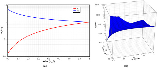
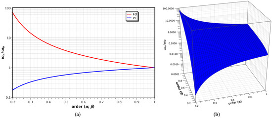
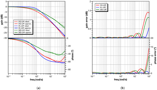
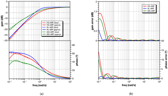
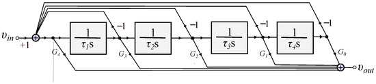
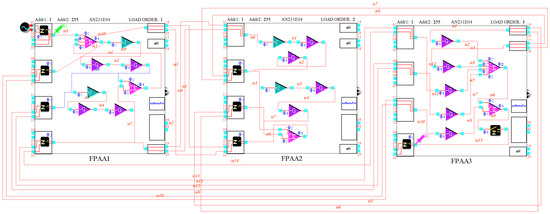
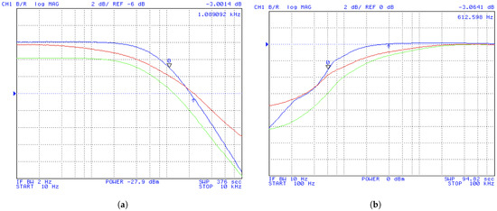
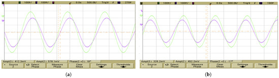
Field Programmable Analog Array Based Non-Integer Filter Designs
by
Alexandros Pagidas, Costas Psychalinos and Ahmed S. Elwakil
Cited by 1 | Viewed by 819
Abstract
The approximation of the frequency behavior of fractional-order, power-law, and double-order filters can be performed by the same rational integer-order transfer function. This can be achieved through the utilization of a curve fitting based approximation. Moreover, their implementation can be performed by the
[...] Read more.
The approximation of the frequency behavior of fractional-order, power-law, and double-order filters can be performed by the same rational integer-order transfer function. This can be achieved through the utilization of a curve fitting based approximation. Moreover, their implementation can be performed by the same core, by only changing the corresponding time constants and scaling factors. The aforementioned findings are experimentally verified using a Field Programmable Analog Array device.
Full article
►▼
Show Figures
Open AccessArticle
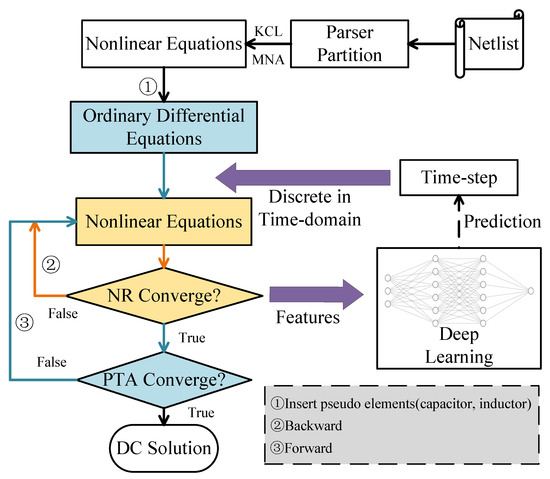
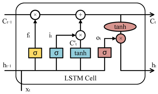
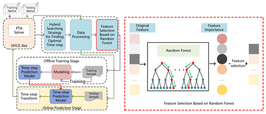
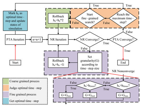
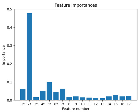
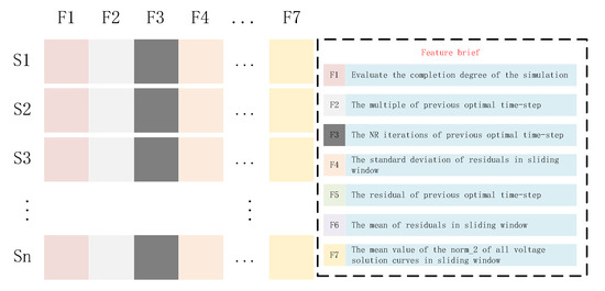
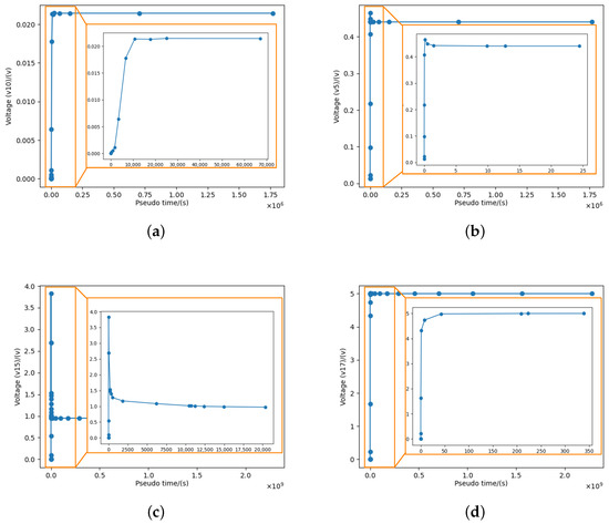
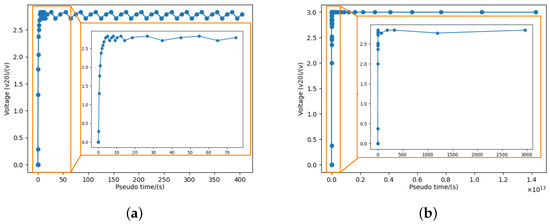
Accelerating DC Circuit Simulation through Feature Selection and LSTM-Based Time-Step Control
by
Zhou Jin, Ziyi Yang, Haojie Pei, Xiaru Zha, Yinuo Bai, Dan Niu, Zhenya Zhou and Xiao Wu
Viewed by 1154
Abstract
Circuit simulation has become increasingly significant in circuit design with the development of very large scale integration, and direct current (DC) analysis, which serves as the basis of circuit behavior analysis, is the foundation for nonlinear electronic circuit simulation. Among the several continuation
[...] Read more.
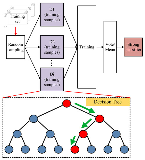
Circuit simulation has become increasingly significant in circuit design with the development of very large scale integration, and direct current (DC) analysis, which serves as the basis of circuit behavior analysis, is the foundation for nonlinear electronic circuit simulation. Among the several continuation algorithms for DC analysis, pseudo-transient analysis (PTA) methods have gained great success. However, PTA tends to be computationally intensive without a proper time-step control method. In order to improve this problem, we propose a novel time-step control method enhanced by advanced deep learning in this paper. Specifically, a coarse and fine-grained hybrid sampling strategy is introduced to find the optimal time step, which resolves the problem that the optimal time step has no precise definition in PTA theory. After that, a long short-term memory (LSTM) network, with the ability to process temporal information, can be employed to learn the optimal time-step control method based on feature selection and a two-stage data preprocessing strategy, which accelerates DC analysis. Furthermore, random forest (RF) is also used to evaluate feature importance, which can achieve feature selection with reduced dimensions, thereby speeding up the network’s training speed and improving the accuracy of prediction. Experimental results demonstrate a significant speedup: up to 61.32 times.
Full article
►▼
Show Figures
Open AccessFeature PaperArticle
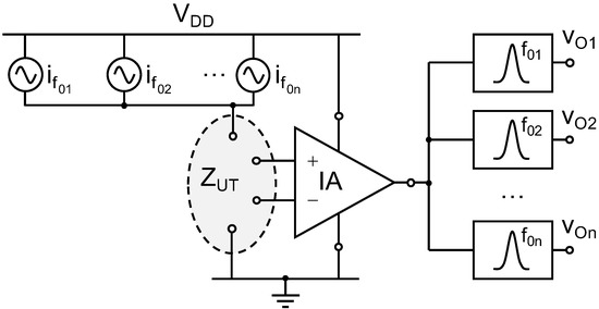
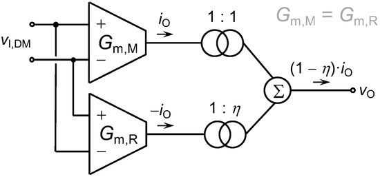
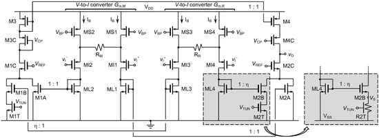
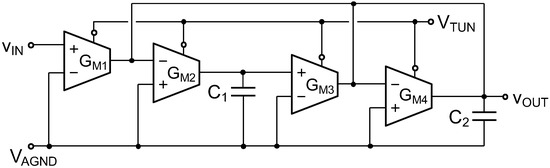
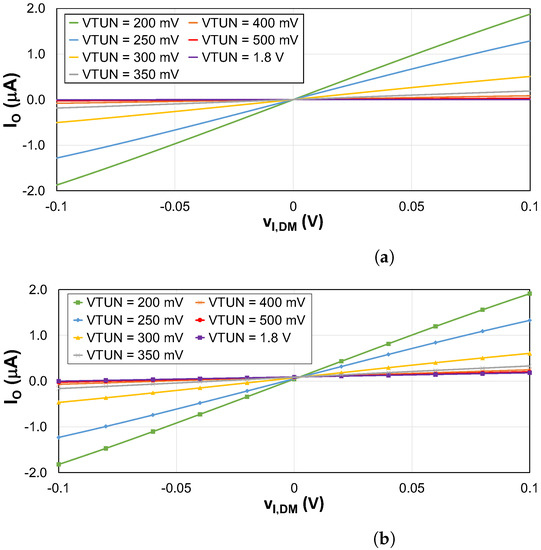
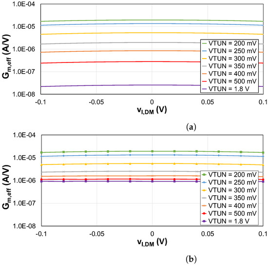
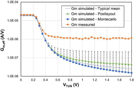
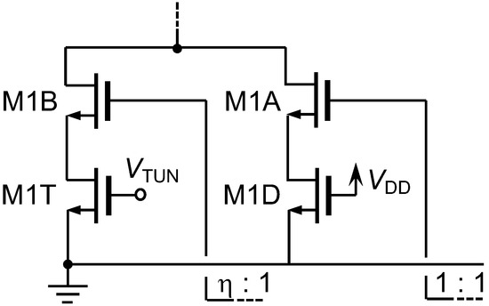
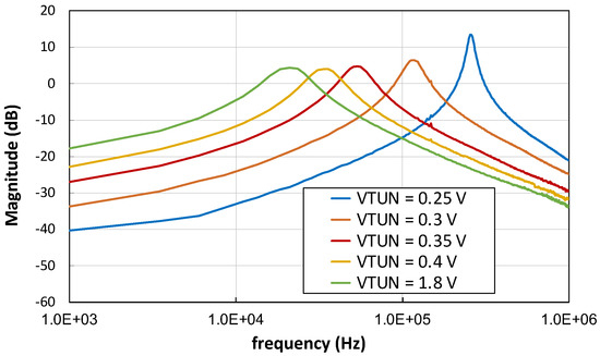
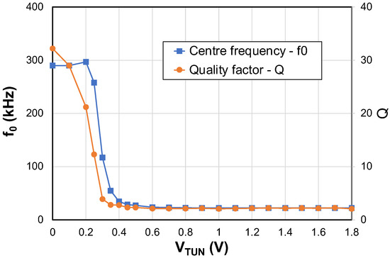
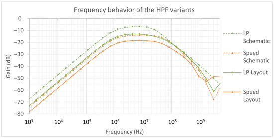
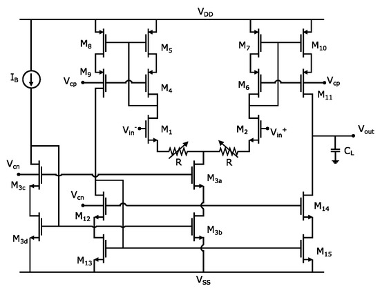
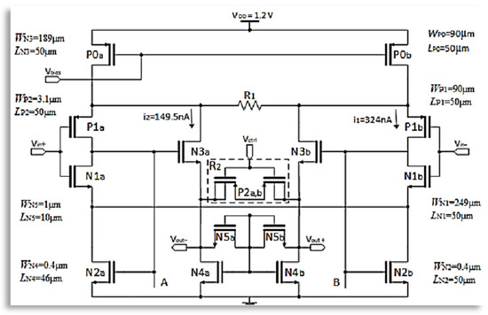
CMOS Widely Tunable Second-Order Gm-C Bandpass Filter for Multi-Sine Bioimpedance Analysis
by
Israel Corbacho, Juan M. Carrillo, José L. Ausín, Miguel Á. Domínguez, Raquel Pérez-Aloe and J. Francisco Duque-Carrillo
Cited by 7 | Viewed by 1150
Abstract
A CMOS widely tunable second-order
-
C bandpass filter (BPF), intended to be used in multi-sine bioimpedance applications, is presented. The filter incorporates a tunable transconductor in which the responses of two linearized voltage-to-current converters are subtracted. As a result, the
[...] Read more.
A CMOS widely tunable second-order
-
C bandpass filter (BPF), intended to be used in multi-sine bioimpedance applications, is presented. The filter incorporates a tunable transconductor in which the responses of two linearized voltage-to-current converters are subtracted. As a result, the effective transconductance can be continuously adjusted over nearly three decades, which allows a corresponding programmability of the center frequency of the BPF. The circuit was designed and fabricated in 180 nm CMOS technology to operate with a 1.8 V supply, and the experimental characterization was carried out over eight samples of the silicon prototype. The simulated transconductance of the cell can be tuned from 5.3 nA/V up to 19.60
A/V. The measured range of the experimental transconductance varied, however, between 1.42
A/V and 20.57
A/V. Similarly, the center frequency of the BPF, which in the simulations ranged from 500 Hz to 342 kHz, can be programmed in the silicon prototypes from 22.4 kHz to 290 kHz. Monte Carlo and corner simulations were carried out to ascertain the origin of this deviation. Besides, the extensive simulation and experimental characterization of the standalone transconductor and the complete BPF are provided.
Full article
►▼
Show Figures
Open AccessArticle
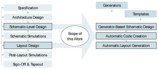
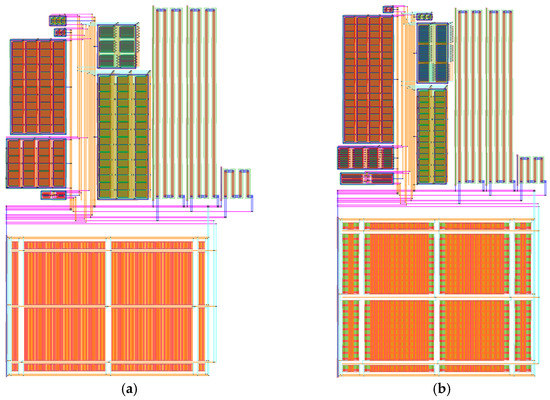
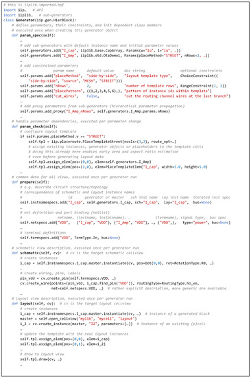
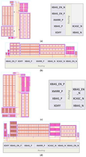
Generating the Generator: A User-Driven and Template-Based Approach towards Analog Layout Automation
by
Benjamin Prautsch, Uwe Eichler and Uwe Hatnik
Viewed by 2407
Abstract
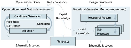
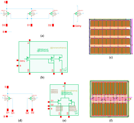
Various analog design automation attempts have addressed the shortcomings of the still largely manual and, thus, inefficient and risky analog design approach. These methods can roughly be divided into synthesis and procedural generation. An important key aspect has, however, rarely been considered: usability.
[...] Read more.
Various analog design automation attempts have addressed the shortcomings of the still largely manual and, thus, inefficient and risky analog design approach. These methods can roughly be divided into synthesis and procedural generation. An important key aspect has, however, rarely been considered: usability. While synthesis requires sophisticated constraints, procedural generators require expert programmers. Both prevent users from adopting the respective method. Thus, we propose a new approach to automatically create procedural generators in a user-driven way. First, analog generators, which also create symbols and layouts, are utilized during schematic entry to encapsulate common analog building blocks. Second, automatic code creation builds a hierarchical generator for all views with the schematic as input. Third, the approach links the building block generators with the layout through an object-oriented template library that is accessible through generator parameters, allowing the user to control the arrangement. No programming is required to reach this state. We believe that our approach will significantly ease the transition of analog designers to procedural generation. At the same time, the templates allow for a “bridge” to open frameworks and synthesis approaches so that the methodologies can be both better spread and combined. This way, comprehensive frameworks of both synthesis-based and procedural-based analog automation methods can be built in a user-driven way, and designers are enabled to gain early layout insight and ease IP reusability.
Full article
►▼
Show Figures
Open AccessArticle
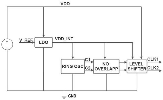
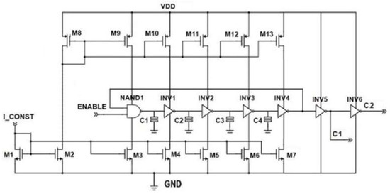
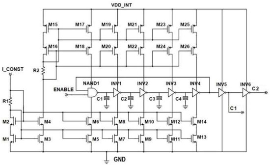
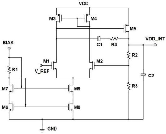
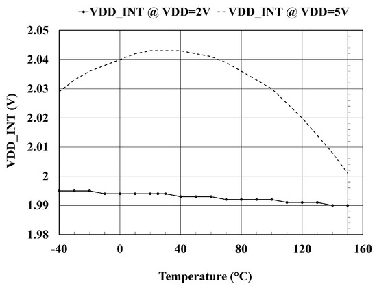
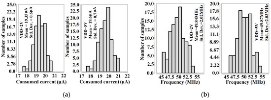
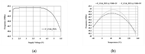
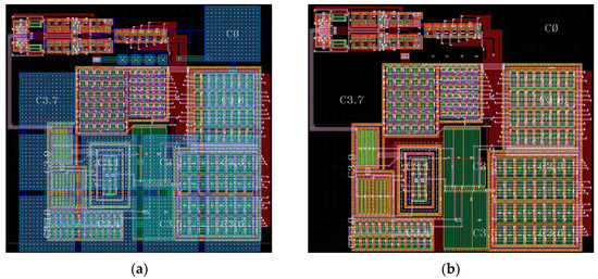
Temperature and Power Supply Compensated CMOS Clock Circuit Based on Ring Oscillator
by
Cristian Stancu, Andrei Neacsu, Ovidiu Profirescu, Dragos Dobrescu and Lidia Dobrescu
Cited by 2 | Viewed by 1835
Abstract
Improved performance operational amplifier demand has continuously increased. IC designers use the charge pump technique as an advanced solution to implement the amplifier’s rail−to−rail input stage, but the need for a large load capacitor is a serious downside. To reduce this passive component
[...] Read more.
Improved performance operational amplifier demand has continuously increased. IC designers use the charge pump technique as an advanced solution to implement the amplifier’s rail−to−rail input stage, but the need for a large load capacitor is a serious downside. To reduce this passive component value, high−frequency clock circuits with a 50% duty cycle should be implemented. This paper focuses on designing such a circuit that is further compensated with temperature and power supply, maintaining these performances even when process variations occur, starting from a ring oscillator as the architecture core. A pre−layout 50 MHz center frequency at 25 °C with a 1.6 temperature percentage error was achieved. Post−layout simulations to account for parasitic effects were also performed, with a 48.9 MHz center frequency reached. Distinct methods that control the frequency variation were discussed and established. Performance comparison of the designed PLL with previously reported clock circuits in the CMOS process was concluded, with superior results such as power consumption, die area, and temperature range accomplished.
Full article
►▼
Show Figures
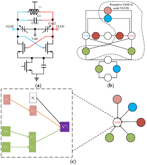
Open AccessArticle
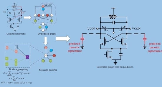
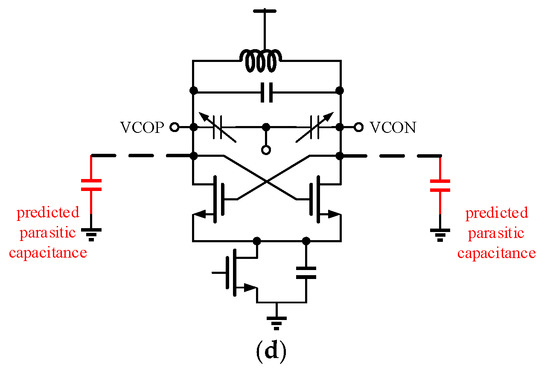
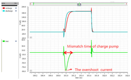
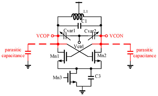
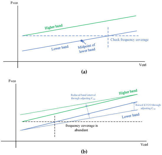
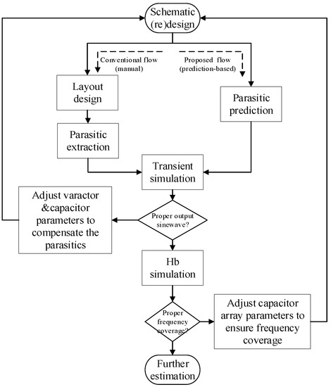
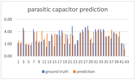
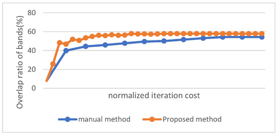
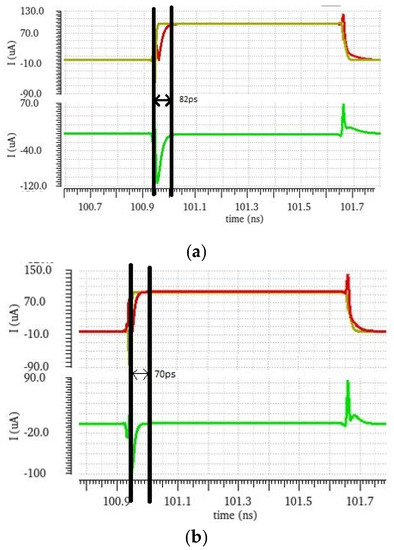
Pre-Layout Parasitic-Aware Design Optimizing for RF Circuits Using Graph Neural Network
by
Chenfeng Li, Dezhong Hu and Xiaoyan Zhang
Viewed by 2001
Abstract
The performance of analog and RF circuits is widely affected by the interconnection parasitic in the circuit. With the progress of technology, interconnection parasitics plays a larger role in performance deterioration. To solve this problem, designers must repeat layout design and validation process.
[...] Read more.
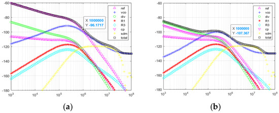
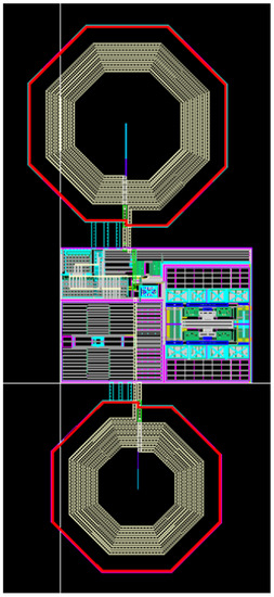
The performance of analog and RF circuits is widely affected by the interconnection parasitic in the circuit. With the progress of technology, interconnection parasitics plays a larger role in performance deterioration. To solve this problem, designers must repeat layout design and validation process. In order to achieve an upgrade in the design efficiency, in this paper, a Graph Neural Network (GNN)-based pre-layout parasitic parameter prediction method is proposed and applied to the design optimization of a 28 nm PLL. With the new method adopted, the frequency band overlap rate of the VCO is improved by 2.3 percents for an equal design effort. Similarly, the optimized CP is superior to the traditional method with a 15 ps mismatch time. These improvements are achieved under the premise of greatly saving the optimization iteration and verification costs.
Full article
►▼
Show Figures
Open AccessArticle
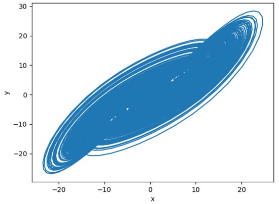
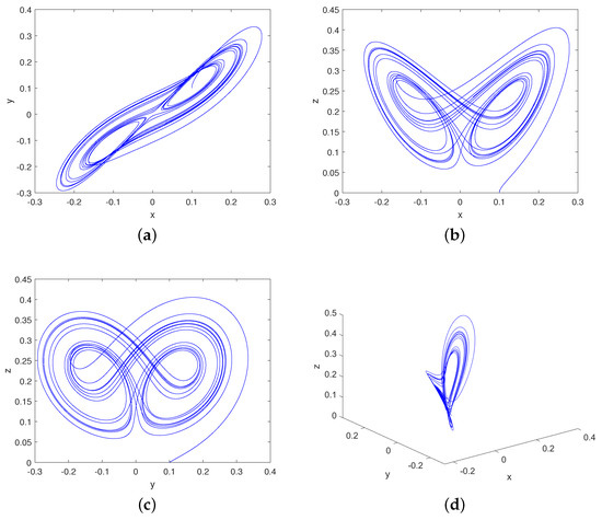
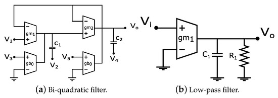
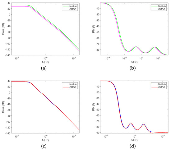
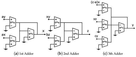
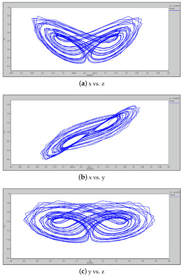
Integrated Circuit Design of Fractional-Order Chaotic Systems Optimized by Metaheuristics
by
Martin Alejandro Valencia-Ponce, Astrid Maritza González-Zapata, Luis Gerardo de la Fraga, Carlos Sanchez-Lopez and Esteban Tlelo-Cuautle
Cited by 7 | Viewed by 1701
Abstract
Nowadays, a huge amount of research is done on introducing and implementing new fractional-order chaotic systems. In the majority of cases, the implementation is done using embedded hardware, and very seldom does it use integrated circuit (IC) technology. This is due to the
[...] Read more.
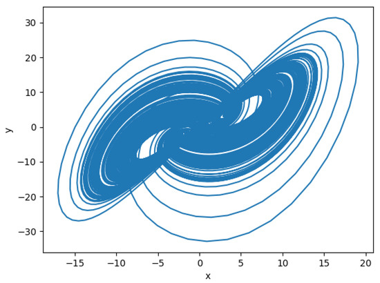
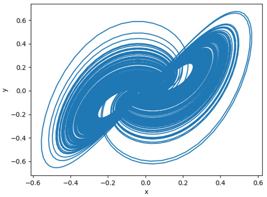
Nowadays, a huge amount of research is done on introducing and implementing new fractional-order chaotic systems. In the majority of cases, the implementation is done using embedded hardware, and very seldom does it use integrated circuit (IC) technology. This is due to the lack of design automation tools ranging from the system level down to layout design. At the system level, the challenge is guaranteeing chaotic behavior by varying all parameters while optimizing dynamical characteristics, such as the Lyapunov spectrum and the Kaplan–Yorke dimension. Using embedded hardware, the implementation is straightforward, but one must perform a scaling process for IC design, in which the biases may be lower than 1 volt but the amplitudes of the state variables of the chaotic systems can have values higher than one. In this manner, this paper describes three levels of abstraction to design fractional-order chaotic systems: The first one shows the optimization of a case study, the mathematical model of the fractional-order Lorenz system to find the fractional-orders of the derivatives, and the coefficients that generate better chaotic behavior. The second level is the block description of a solution of the mathematical model, in which the fractional-order derivatives are approximated in the Laplace domain by several approximation methods. The third level shows the IC design using complementary metal–oxide–semiconductor (CMOS) technology. The transfer functions approximating the fractional-order derivatives are synthesized by active filters that are designed using operational transconductance amplifiers (OTAs). The OTAs are also used to design adders and subtractors, and the multiplication of variables is done by designing a CMOS four-quadrant multiplier. The paper shows that the simulation results scaling the mathematical model to have amplitudes lower than ±1 are in good agreement with the results using CMOS IC technology of 180 nm.
Full article
►▼
Show Figures
Open AccessArticle
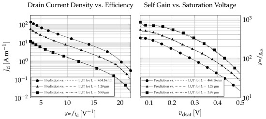
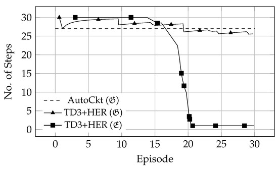
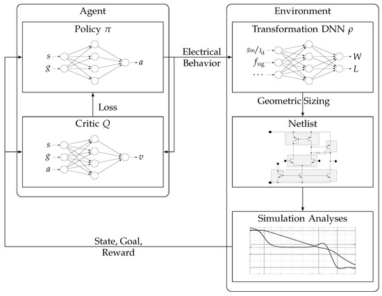
Procedural- and Reinforcement-Learning-Based Automation Methods for Analog Integrated Circuit Sizing in the Electrical Design Space
by
Yannick Uhlmann, Michael Brunner, Lennart Bramlage, Jürgen Scheible and Cristóbal Curio
Cited by 5 | Viewed by 2374
Abstract
Analog integrated circuit sizing is notoriously difficult to automate due to its complexity and scale; thus, it continues to heavily rely on human expert knowledge. This work presents a machine learning-based design automation methodology comprising pre-defined building blocks such as current mirrors or
[...] Read more.
Analog integrated circuit sizing is notoriously difficult to automate due to its complexity and scale; thus, it continues to heavily rely on human expert knowledge. This work presents a machine learning-based design automation methodology comprising pre-defined building blocks such as current mirrors or differential pairs and pre-computed look-up tables for electrical characteristics of primitive devices. Modeling the behavior of primitive devices around the operating point with neural networks combines the speed of equation-based methods with the accuracy of simulation-based approaches and, thereby, brings quality of life improvements for analog circuit designers using the
method. Extending this procedural automation method for human design experts, we present a fully autonomous sizing approach. Related work shows that the convergence properties of conventional optimization approaches improve significantly when acting in the electrical domain instead of the geometrical domain. We, therefore, formulate the circuit sizing task as a sequential decision-making problem in the alternative electrical design space. Our automation approach is based entirely on reinforcement learning, whereby abstract agents learn efficient design space navigation through interaction and without expert guidance. These agents’ learning behavior and performance are evaluated on circuits of varying complexity and different technologies, showing both the feasibility and portability of the work presented here.
Full article
►▼
Show Figures
Open AccessArticle
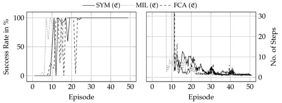
Differentiable Constraints’ Encoding for Gradient-Based Analog Integrated Circuit Placement Optimization
by
António Gusmão, Pedro Alves, Nuno Horta, Nuno Lourenço and Ricardo Martins
Viewed by 1256
Abstract
Analog IC design is characterized by non-systematic re-design iterations, often requiring partial or complete layout re-design. The layout task usually starts with device placement, where the several performance figures and constraints to be met escalate its complexity immensely, and, due to the inherent
[...] Read more.
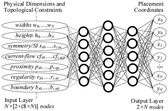
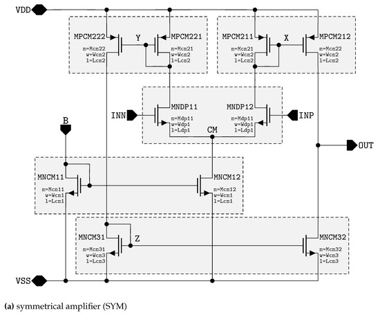
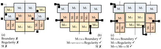
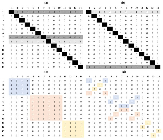
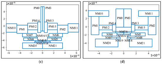
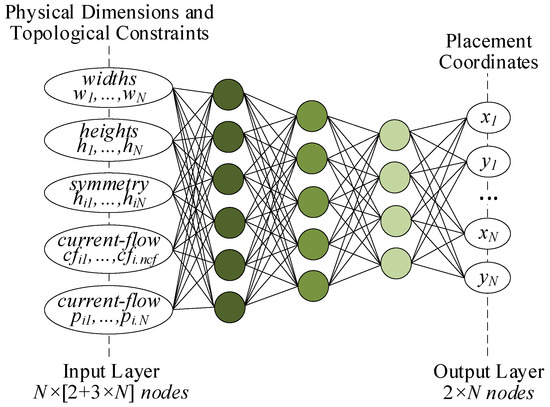
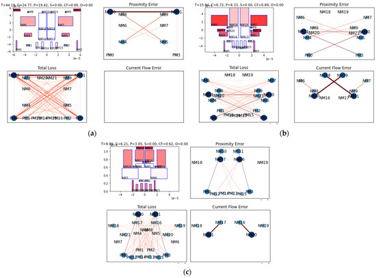
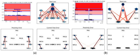
Analog IC design is characterized by non-systematic re-design iterations, often requiring partial or complete layout re-design. The layout task usually starts with device placement, where the several performance figures and constraints to be met escalate its complexity immensely, and, due to the inherent tradeoffs, an “optimal” floorplan solution does not usually exist. Deep learning models are now establishing for the automation of the placement task of analog integrated circuit layout design, promising to bypass the limitations of existing approaches based on: time-consuming optimization processes with several constraints; or placement retargeting from legacy designs/templates, which rely heavily on legacy layout data. However, as the complexity of analog design cases tackled by these methodologies increases, a broader set of topological constraints must be supported to cover the different layout styles and circuit classes. Here, model-independent differentiable encodings for regularity, boundary, proximity, and symmetry island constraints are formulated for the first time in the literature, and an unsupervised loss function is used for the artificial neural network model to learn how to generate placements that follow them. The use of a deep learning model makes push-button speed placement generation possible, additionally, as only sizing data are required for its training, it discards the need to acquire legacy layouts containing insights into this vast set of, often neglected, constraints. The model is ultimately used to produce floorplans from scratch at push-button speed for real state-of-the-art analog structures, including technology nodes not used for training. A case-study comparison with a floorplan design made by a human-expert presents improvements in the fulfillment of every constraint, reaching an overall improvement of around 70%, demonstrating the approach’s value in placement design.
Full article
►▼
Show Figures
Open AccessFeature PaperArticle
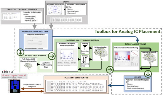
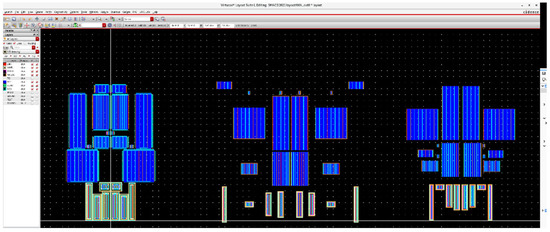
Exploiting a Deep Learning Toolbox for Human-Machine Feedback towards Analog Integrated Circuit Placement Automation
by
António Gusmão, Rafael Vieira, Nuno Horta, Nuno Lourenço and Ricardo Martins
Cited by 1 | Viewed by 1604
Abstract
The layout design of analog integrated circuits has been defying all automation attempts, and it is still primarily a handcrafting process carried by circuit designers on traditional layout editing frameworks. This paper presents a toolbox based on deep learning techniques and a sturdy
[...] Read more.
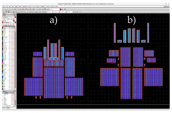
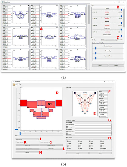
The layout design of analog integrated circuits has been defying all automation attempts, and it is still primarily a handcrafting process carried by circuit designers on traditional layout editing frameworks. This paper presents a toolbox based on deep learning techniques and a sturdy graphical user interface to assist designers during that process. The underlying mechanism of this toolbox relies on a simple pairwise device interaction circuit description, i.e., the circuits’ topological constraints, to propose valid floorplan solutions for block-level structures, including topologies and deep nanometer technology nodes not used for its training, at push-button speed. Despite its automatic functionalities, the toolbox is focused on explainable artificial intelligence, involving the designer in the synthesis flow via filtering and editing options over the candidate floorplan solutions. This constant state of human-machine feedback environment turns the designer aware of the impact of each device’s position change and inherent tradeoffs while suggesting subsequent moves, ultimately increasing the designers’ productivity in this time-consuming and iterative task. Finally, the toolbox is shown to instantly generate floorplans with similar or better constraint fulfilment than human designed solutions for state-of-the-art analog circuit blocks.
Full article
►▼
Show Figures
Open AccessArticle
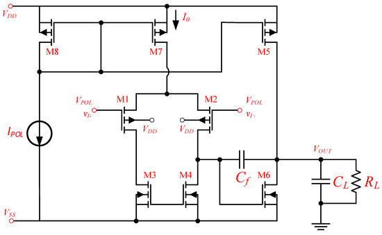
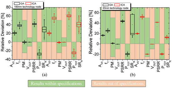
Customized Imperialist Competitive Algorithm Methodology to Optimize Robust Miller CMOS OTAs
by
Egon Henrique Salerno Galembeck, Salvador Pinillos Gimenez and Rodrigo Alves de Lima Moreto
Cited by 1 | Viewed by 1192
Abstract
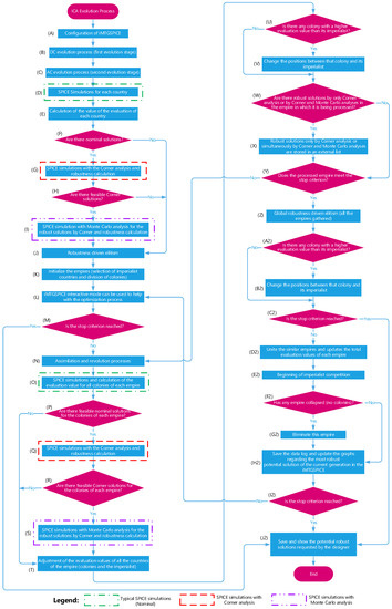
The design and optimization of the analog complementary metal-oxide-semiconductor (CMOS) integrated circuits (ICs) are intrinsically complicated and depend heavily on the designer’s experience, and are associated with very long design and optimization-cycle times. In addition, in order to the analog and radiofrequency (RF)
[...] Read more.
The design and optimization of the analog complementary metal-oxide-semiconductor (CMOS) integrated circuits (ICs) are intrinsically complicated and depend heavily on the designer’s experience, and are associated with very long design and optimization-cycle times. In addition, in order to the analog and radiofrequency (RF) CMOS IC work suitably in practice, it is necessary to perform robustness analyses (RAs) through Simulation Program with Integrated Circuit Emphasis (SPICE) simulations, which result in still-higher design and optimization cycle times and therefore represent the biggest bottleneck to the launching of new electronic products. In this context, this manuscript aims to present, for the first time, the use of a custom imperialist competitive algorithm (ICA) in order to reduce the design and optimization-cycle times of analog CMOS ICs. In this study, we implement some Miller CMOS operational transconductance amplifiers (OTAs) using the computational tool named iMTGSPICE, considering two different bulk CMOS IC manufacturing processes from Taiwan Semiconductor Company (TSMC) (180 nm and 65 nm nodes) and two evolutionary optimization methodologies of artificial intelligence, i.e., ICA and a genetic algorithm (GA). The main result obtained by this work shows that, by using an ICA-customized evolutionary algorithm to perform the design and optimization processes of Miller CMOS OTAs, it is possible to reduce the design and optimization-cycle times by up to 83% in relation to those implemented with the GA-customized evolutionary algorithm, achieving practically the same electrical performance.
Full article
►▼
Show Figures
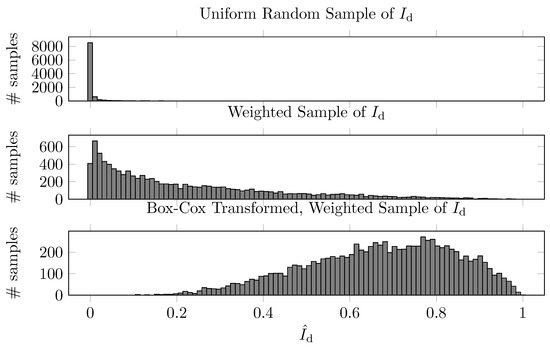
Open AccessArticle
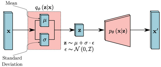
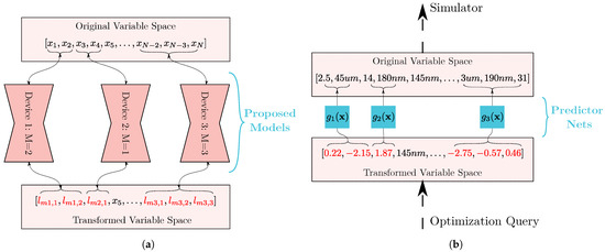
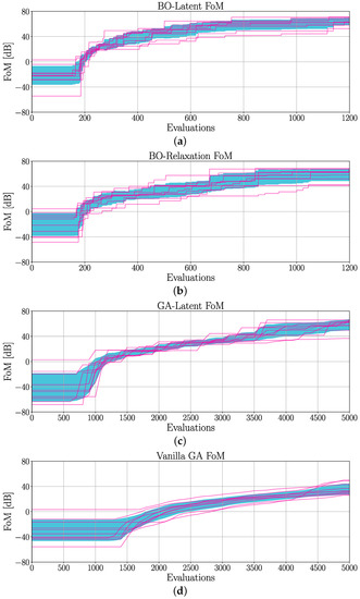
Mixed-Variable Bayesian Optimization for Analog Circuit Sizing through Device Representation Learning
by
Kostas Touloupas and Paul Peter Sotiriadis
Viewed by 1515
Abstract
In this work, a deep representation learning method is proposed to build continuous-valued representations of individual integrated circuit (IC) devices. These representations are used to render mixed-variable analog circuit sizing problems as continuous ones and to apply a low-budget black box Bayesian optimization
[...] Read more.
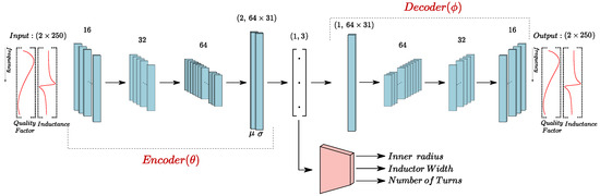
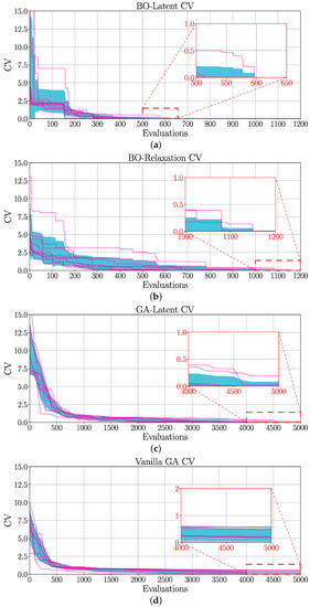
In this work, a deep representation learning method is proposed to build continuous-valued representations of individual integrated circuit (IC) devices. These representations are used to render mixed-variable analog circuit sizing problems as continuous ones and to apply a low-budget black box Bayesian optimization (BO) variant to solve them. By transforming the initial search spaces into continuous-valued ones, the BO’s Gaussian process models (GPs), which typically operate on real-valued spaces, can be used to guide the optimization search towards the global optimum. The proposed Device Representation Learning approach involves using device simulation data and training a composite model of a Variational Autoencoder (VAE) and a dense Neural Network. The latent variables of the trained VAE model serve as the representations of the integrated device and replace the discrete-valued parametrizations of particular devices. A thorough explanation of the proposed methodology’s mathematical formulation is given and example sizing applications on real-world analog circuits and integrated devices underline its efficiency.
Full article
►▼
Show Figures
Open AccessArticle
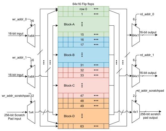
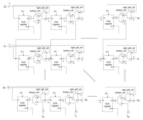
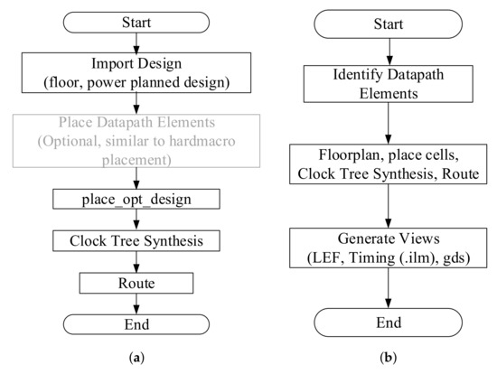
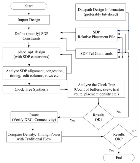
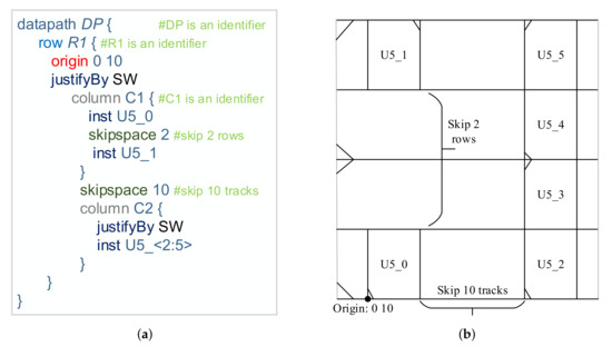
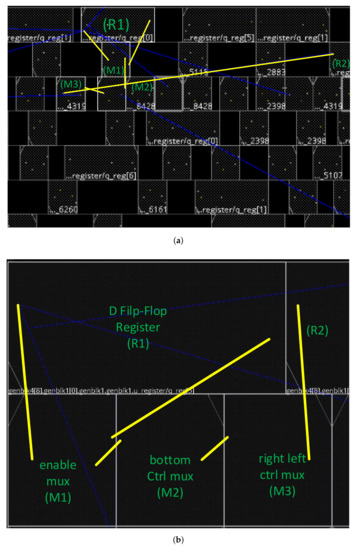
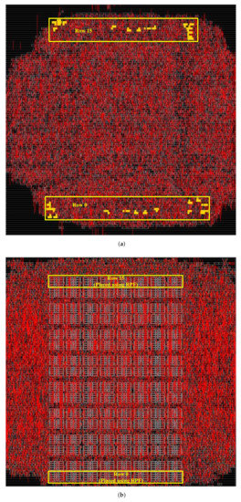
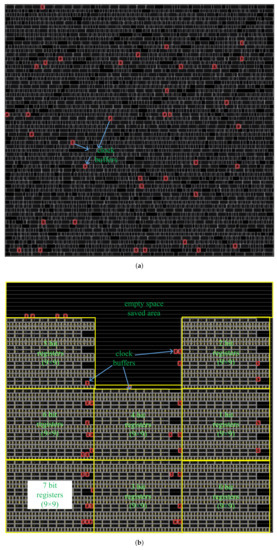
Methodology for Structured Data-Path Implementation in VLSI Physical Design: A Case Study
by
Dhilleswararao Pudi, Samuel Jigme Harrison, Dimitrios Stathis, Srinivas Boppu, Ahmed Hemani and Linga Reddy Cenkeramaddi
Cited by 1 | Viewed by 2677
Abstract
State-of-the-art modern microprocessor and domain-specific accelerator designs are dominated by data-paths composed of regular structures, also known as bit-slices. Random logic placement and routing techniques may not result in an optimal layout for these data-path-dominated designs. As a result, implementation tools such as
[...] Read more.
State-of-the-art modern microprocessor and domain-specific accelerator designs are dominated by data-paths composed of regular structures, also known as bit-slices. Random logic placement and routing techniques may not result in an optimal layout for these data-path-dominated designs. As a result, implementation tools such as Cadence’s Innovus include a Structured Data-Path (SDP) feature that allows data-path placement to be completely customized by constraining the placement engine. A relative placement file is used to provide these constraints to the tool. However, the tool neither extracts nor automatically places the regular data-path structures. In other words, the relative placement file is not automatically generated. In this paper, we propose a semi-automated method for extracting bit-slices from the Innovus SDP flow. It has been demonstrated that the proposed method results in 17% less density or use for a pixel buffer design. At the same time, the other performance metrics are unchanged when compared to the traditional place and route flow.
Full article
►▼
Show Figures
Open AccessCommunication
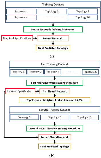
Fast Topology Selection for Analog Amplifier Circuits Using On-The-Fly Cascaded Neural Networks
by
Karim Khalil, Khaled Yasseen and Hesham Omran
Cited by 2 | Viewed by 2054
Abstract
In this paper, a machine learning-based approach for the automation of topology selection of integrated analog amplifier circuits is presented. A dataset of 480,000 circuits for 30 different amplifier topologies is generated for the prediction algorithm based on a precomputed lookup tables (LUTs)
[...] Read more.
In this paper, a machine learning-based approach for the automation of topology selection of integrated analog amplifier circuits is presented. A dataset of 480,000 circuits for 30 different amplifier topologies is generated for the prediction algorithm based on a precomputed lookup tables (LUTs) approach. A first approach based on neural networks is presented where the required specifications act as inputs to the networks, and the output of the network is the suitable topology for such a set of specifications. A modified cascaded neural network approach is examined to reduce the training time of the network while maintaining the prediction accuracy. Using the cascaded neural network approach, the network is trained in only one minute on a standard computer, and a 90.8% prediction accuracy is achieved. This allows on-the-fly changes in the input specifications, and consequently the neural network, to enable examining different design scenarios.
Full article
►▼
Show Figures
Open AccessArticle
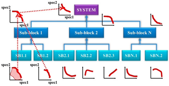
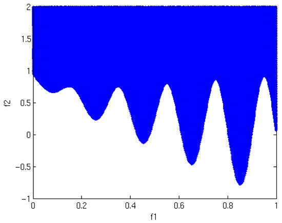
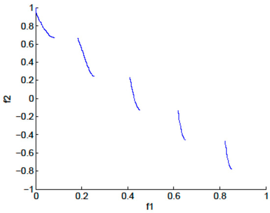
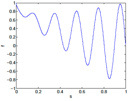
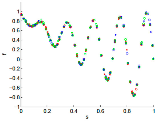
Addressing a New Class of Multi-Objective Passive Device Optimization for Radiofrequency Circuit Design
by
Fabio Passos, Elisenda Roca, Rafael Castro-López and Francisco V. Fernández
Viewed by 1128
Abstract
The design of radiofrequency circuits and systems lends itself to multi-objective optimization and the bottom-up composition of Pareto-optimal fronts. Conventional multi-objective optimization algorithms can effectively attain these fronts, which maximize or minimize a set of competing objective functions of interest. However, some of
[...] Read more.
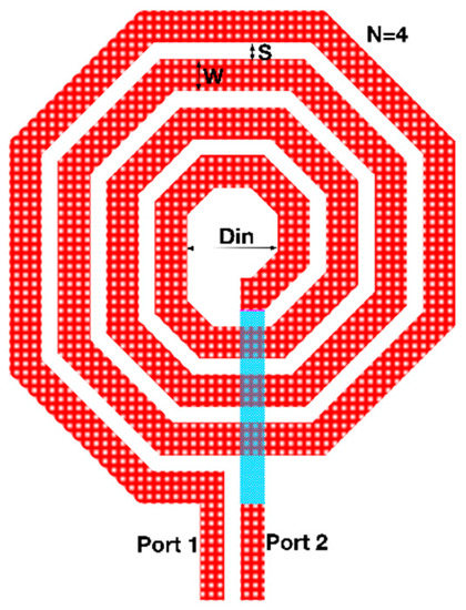
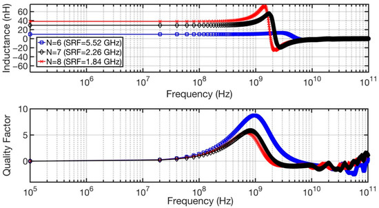
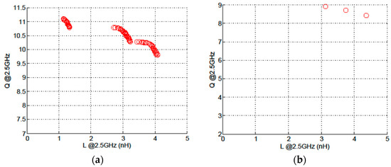
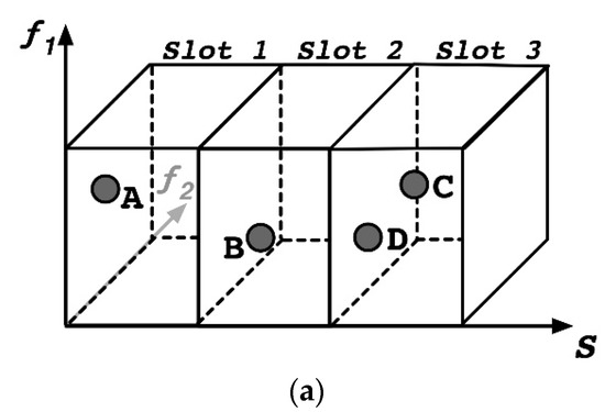
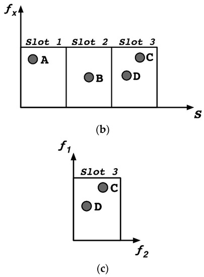
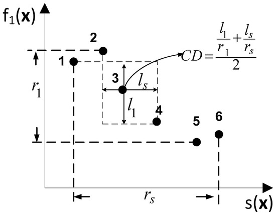
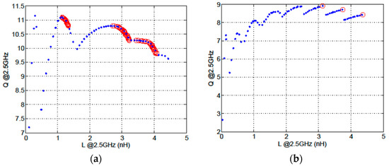
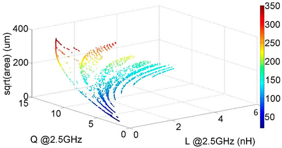
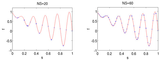
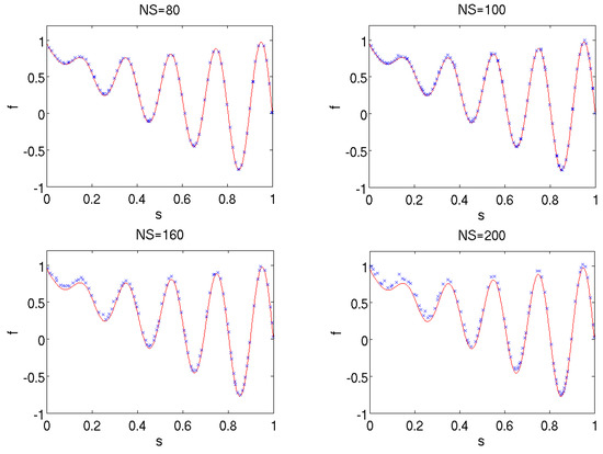
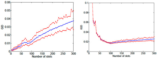
The design of radiofrequency circuits and systems lends itself to multi-objective optimization and the bottom-up composition of Pareto-optimal fronts. Conventional multi-objective optimization algorithms can effectively attain these fronts, which maximize or minimize a set of competing objective functions of interest. However, some of these real-life optimization problems reveal a non-conventional feature: there is one objective function that calls neither for minimization nor maximization. Instead, using the Pareto front demands this objective function to be swept across so that all its feasible values are available. Such a non-conventional feature, as shown here, emerges in the case of inductor optimization. The problem thus turns into a non-conventional one: determining how to find uniformly distributed feasible values of this function over the broadest possible range (typically unknown) while minimizing or maximizing the remaining competing objective functions. An NSGA-II-inspired algorithm is proposed that, based on the dynamic allocation of objective function slots and a modified dominance definition, can successfully return sets of solutions for inductor optimization problems with one sweeping objective. Furthermore, a mathematical benchmark function modeling this kind of problem is presented, which is also used to exhaustively test the proposed algorithm and obtain insight into its parameter settings.
Full article
►▼
Show Figures
Open AccessArticle
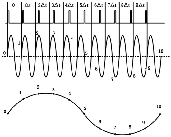
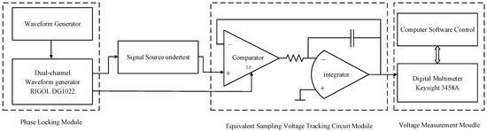
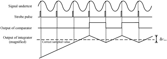
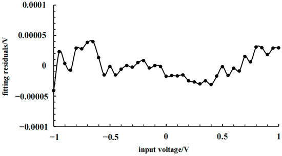
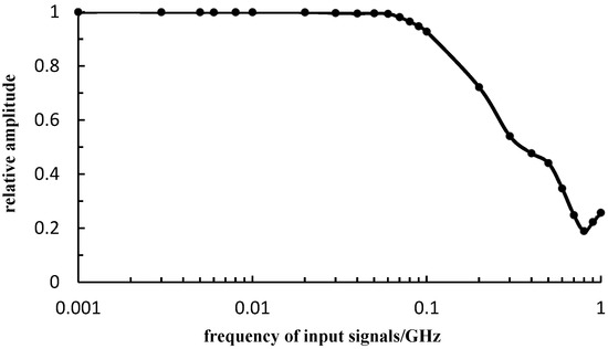
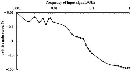
Precision Measurement System of High-Frequency Signal Based on Equivalent-Time Sampling
by
Xiaoxuan Zang, Jianting Zhao, Yunfeng Lu and Qing He
Cited by 3 | Viewed by 2337
Abstract
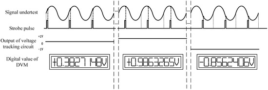
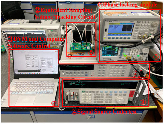
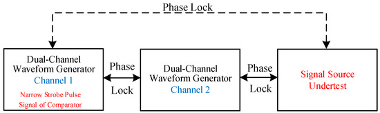
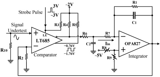
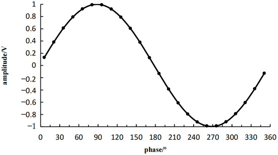
A high frequency periodic signal measurement system based on equivalent sampling method is developed. A high-speed sampling voltage tracking circuit, the core component of the system, is described in detail. The circuit can transform the amplitude corresponding to different phase points of the
[...] Read more.
A high frequency periodic signal measurement system based on equivalent sampling method is developed. A high-speed sampling voltage tracking circuit, the core component of the system, is described in detail. The circuit can transform the amplitude corresponding to different phase points of the signal undertest into the equivalent DC level through successive approximation of multiple periods. The measurement system designed in this paper completes digital sampling with high accuracy only by connecting the low-cost voltage tracking circuit to the existing commercial instruments, such as two-channel waveform generator and high-precision digital multimeter, which makes the method easy to be generalized. The special structure of the sampling tracking circuit greatly reduces the influence of random noise and time jitter on the measurement results. The experimental results show that the non-linearity error of the system is as low as 0.002%, the bandwidth can reach 200 MHz, and the uncertainty of measuring the RMS of AC voltage with peak value of ±1 V and frequency of 10 kHz, 100 kHz and 1 MHz can reach 2.8 × 10
−4 V, 4.6 × 10
−4 V and 2.0 × 10
−4 V (k = 2), respectively.
Full article
►▼
Show Figures
Planned Papers
The below list represents only planned manuscripts. Some of these
manuscripts have not been received by the Editorial Office yet. Papers
submitted to MDPI journals are subject to peer-review.
Title: Exploiting a Deep Learning Toolbox for Human-Machine Feedback towards Analog Integrated Circuit Placement Automation
Authors: António Gusmão; Rafael Vieira; Nuno Horta; Nuno Lourenço; Ricardo Martins
Affiliation: Instituto de Telecomunicações, Instituto Superior Técnico, Av. Rovisco Pais, 1049-001 Lisboa, Portugal
Abstract: The layout design of analog integrated circuits has been defying all automation attempts, and it is still primarily a handcrafting process carried by circuit designers on traditional layout ed-iting frameworks. This paper presents a toolbox based on deep learning techniques and a sturdy graphical user interface to assist designers during that process. The underlying mechanism of this toolbox relies on a simple pair-wise device interaction circuit description, i.e., the circuits’ topolog-ical constraints, to propose valid floorplan solutions for block-level structures, including topologies and deep technology nodes not used for its training, at push-button speed. Despite its automatic functionalities, the toolbox is focused on explainable artificial intelligence, involving the designer in the synthesis flow via filtering and editing options over the candidate floorplan solutions. This constant state of human-machine feedback environment turns the designer aware of the impact of each device’s position change and inherent tradeoffs while suggesting subsequent moves, ultimately increasing the designers’ productivity in this time-consuming and iterative task. Finally, the toolbox is shown to instantly generate floorplans with better constraint fulfilment than human designed solutions for state-of-the-art analog circuit blocks.
Title: Modeling the Avalanche Breakdown of FMMT417 NPN Transistor in the TINA Environment
Authors: Mert Yetkin; Mustafa Berke Yelten
Affiliation: 1. ASELSAN Incorporation, Turkey
2. Istanbul Technical University
Abstract: In this paper, the avalanche breakdown observed in avalanche-type bipolar junction transistors is modeled where a macromodel proposed earlier in the literature is extended to become compatible with practical circuit simulators. Moreover, contributions to the macromodel are introduced and implemented. The resulting model is used in circuit simulations, and the outcomes are compared with the experimental results that depict the accuracy of the proposed approach.
Title: Impact The Use Of The Customized Imperialist Competitive Algorithm To Optimize Robust Miller CMOS Otas
Authors: Rodrigo Alves de Lima Moreto; Egon Henrique Salerno Galembeck; Salvador Pinillos Gimenez
Affiliation: FEI, São Paulo, Brazil
Abstract: The design and optimization of the analog complementary metal-oxide-semiconductor (CMOS) integrated circuits (ICs) are intrinsically complicated and rely heavily on the designer's experience, associated with a long design and optimization cycle time. In addition, in order to the analog CMOS ICs work suitably in the practice, it is necessary to perform the robustness analyses (RAs) through the SPICE simulations, that results a higher design and optimization cycle time, and therefore, represents the biggest bottleneck to the launching new electronic products. In this context, this manuscript aims to present, for the first time, the use of a custom Imperialist Competitive Algorithm (ICA) in order to reduce the design and optimization cycle time of the analog CMOS ICs. In this study we implement some Miller Operational Transconductance Amplifiers (OTAs) by using the computational tool named iMTGSPICE, considering the 180nm and 65nm manufacturing processes of Taiwan Semiconductor Company (TSMC) and two optimization heuristic methodologies of Artificial Intelligence, i.e. ICA and Genetic Algorithm (GA). The main result obtained by this work have showed that, by using ICA heuristic algorithm to perform the design and optimization processes of Miller CMOS OTAs, it is possible to reduce the design and optimization cycle time by up to 83% in relation to those implemented with the customized GA heuristic algorithm, keeping practically the same their electrical performances and robustness.

