Article

Temperature and Power Supply Compensated CMOS Clock Circuit Based on Ring Oscillator

Department of Electronic Devices, Circuits and Architectures, Faculty of Electronics, Telecommunications and Information Technology, University Politehnica of Bucharest, 060042 Bucharest, Romania
*
Author to whom correspondence should be addressed.
Electronics 2023, 12(3), 507; https://doi.org/10.3390/electronics12030507
Submission received: 25 November 2022 / Revised: 12 January 2023 / Accepted: 13 January 2023 / Published: 18 January 2023

Abstract

:
Improved performance operational amplifier demand has continuously increased. IC designers use the charge pump technique as an advanced solution to implement the amplifier’s rail−to−rail input stage, but the need for a large load capacitor is a serious downside. To reduce this passive component value, high−frequency clock circuits with a 50% duty cycle should be implemented. This paper focuses on designing such a circuit that is further compensated with temperature and power supply, maintaining these performances even when process variations occur, starting from a ring oscillator as the architecture core. A pre−layout 50 MHz center frequency at 25 °C with a 1.6 temperature percentage error was achieved. Post−layout simulations to account for parasitic effects were also performed, with a 48.9 MHz center frequency reached. Distinct methods that control the frequency variation were discussed and established. Performance comparison of the designed PLL with previously reported clock circuits in the CMOS process was concluded, with superior results such as power consumption, die area, and temperature range accomplished.

1. Introduction

Operational amplifiers (Op−amps) in CMOS technology have evolved from classical differential stages with active load and single−ended output [1] into complex architectures that minimize the offset voltage V O S and the noise spectral density, with simultaneous cost reduction and improved performance. New state−of−the−art topologies are frequently developed alongside CMOS technology with continuous improvement (decreasing the leakage currents or the transistor die size, for example). A main topic currently is finding the most efficient approach to implement the amplifier rail−to−rail input stage.
One common design solution uses complementary p M O S n M O S differential input pairs with architectures that control the transistor currents, to maintain constant transconductance g m for the whole input range. Some topologies are presented in [2], but one of this method’s disadvantages is the offset voltage, which is slightly different from stage to stage. A further drawback that must be considered is the variable transconductance in the regions where the transition between the complementary input stages occurs due to the current that passes from one branch to another.
Another more valuable approach implies using charge pump circuits that level up the potential around the input stage with a known value above supply voltage ( V D D ). In this case, one single differential pair is active for the entire common input range; thus, no complementary pair is longer required. The transconductance and the offset voltage in this situation will be constant regardless of what signal is applied at the transistor’s input.
Charge pump architectures are based on clock signals and fast switching to charge/discharge capacitors to obtain higher voltages than the supply. A popular topology is the Dickson charge pump [3,4], but more optimized and efficient circuits have now been established. One downside of this approach is the higher currents that must be drawn from the charge pump output, mainly the differential pair tail current, but additional currents may be needed depending on the designer’s approach. This will require large load capacitances to maintain a low ripple voltage at the circuit output; accordingly, the circuit die size will increase.
A key idea in solving this inconvenience and therefore having a lower capacitance value is reaching a clock frequency where the power supply rejection ratio (PSRR) in alternative current (AC) is high enough that the ripple at the amplifier’s output will be considerably reduced. This usually happens at frequencies on the order of tens of MHz; thus, oscillators that can reach such high oscillation period values with lower current consumption and die area must be implemented.
Another aspect to remember in the oscillator design stages used in a charge−pump architecture is the frequency process variation. The differential input tail current in an op−amp has a PTAT characteristic, so that the transconductance is compensated with temperature; thus, a constant unity gain bandwidth (UGBW) and an improved offset voltage thermal coefficient (TCVOS) are obtained. In corners, this current is lower, slow−slow process (SS), respective to the higher, fast−fast process (FF). Frequency process compensation would lead, for example, in FF to higher charge−pump ripple at its output, which is undesirable in a precision op−amp architecture.
Designing relaxation oscillators [5,6], for example, is not suitable because, first and foremost, to obtain 50% duty cycles with this approach, frequency divider circuits (DFF) are required, finally leading to two times higher clock period values. Furthermore, higher frequencies will conduce to an increase in their dependence on the delay given by the signal’s propagation through the circuits, which is unacceptable for applications where the frequency oscillation must be accurately determined.
This paper presents an innovative clock circuit concept that eliminates the abovementioned impediments and achieves compensation with temperature and power supply, maintaining these performances even when process variations occur. The block diagram is presented in Figure 1. Clock architecture is accomplished based on a ring oscillator circuit [7,8,9]. The frequency dependence given by the supply voltage is reduced using a low−dropout regulator (LDO). One non−overlapping circuit is also implemented alongside a level shifter block [10] that restores the clock signal’s maximum value. V R E F is a reference potential established by using a bandgap voltage. Cascaded current−starved mirrors are used to fulfill temperature compensation. The circuit works at high temperatures (maximum 150 °C), so that its applicability is extended to the automotive industry.

2. Design and Implementation

2.1. Classical Current Starved Ring VCO

This subchapter presents the well−known current starved ring VCO that is the starting point [11] for the improved and more efficient architecture presented in this paper. The schematic is presented in Figure 2. One NAND gate provides an on−and−off switching option for the circuit. When the enable pin is “0” logic, the NAND gate output will remain “1”, regardless of what signal is on the other input; thus, no oscillation will occur. When the enable pin is “1”, the NAND gate will behave identically as an inverter, creating favorable conditions for oscillation appearance. Odd numbers of logical gates are required in the reaction loop. Capacitors C 1 C 4 are added to further control the output frequency [7]:
t c a p = C V t h I c o n t
where V t h is the inverter threshold point, C the capacitor value, and I c o n t the current that passes through the inverter.
The generated signal period is [7]:
T c l k = 2 ( t n a n d + 4 t i n v + 4 t c a p )
where t n a n d is the NAND logic gate delay time and t i n v is the inverter logic gate delay time.
This architectures downside is that M1 and M8 transistors are in diode configuration. Thus their drain−source voltage is well fixed and equal to their gate−source voltage, while nMOS transistors M2–M7 and pMOS transistors M9–M13 VDS are supply voltage dependent. This will cause a shift in the logic gates propagation delay and the C1−C4 capacitor’s charge/discharge time with the supply voltage, given by the drain current short−channel effect; hence the ring VCO frequency is affected. Moreover, the gate−source voltage of the M1 and M8 transistors is complementary to absolute temperature (CTAT), leading to a change in frequency with temperature.

2.2. Proposed Ring Oscillator Technique

The proposed ring oscillator technique keeps the current mirror drain−source voltage equal, regardless of the supply voltage and temperature. Figure 3 shows the proposed architecture. p M O S n M O S cascade current mirror pairs have been implemented. Using this topology complementary with designing a zero to absolute temperature (ZTAT) current, the switching current is well controlled, and compensation with temperature is achieved.
The logic gate delay time is strongly influenced by the circuit supply voltage due to the gate potential that is detected by each transistor. As a result of using the cascade current mirrors, the established potential in the sources of p M O S and n M O S devices, which forms the logic gates in the ring oscillator, are not connected directly to V D D and G N D :
V S n m o s = V D S _ N c a s c a d e + V D S _ N m i r r o r
V S p m o s = V D D V S D _ P m i r r o r V S D _ P c a s c a d e
The current mirror V D S voltage is well determined by the potentials across R 1 and R 2 resistors. On the other hand, the cascades V D S is not biased at a fixed point; thus, variations with switching the supply voltage may occur. This can cause a change in the logic gate’s delay time, and fluctuations in the oscillation frequency are expected. To avoid such inconvenience, an internal 2 V voltage compensated with temperature and V D D is used.
A 50% duty cycle is ensured by fixing the logic gates’ threshold points at half of V D D when they were simulated independently. The desired clock frequency in this paper is 50 MHz at room temperature. Transistor dimensions and other component values that form the ring oscillator are charted in Table 1.

2.3. Low—Dropout Voltage Concept

The L D O circuit is established by using a two−stage operational amplifier [12,13], as seen in Figure 4. transistors M 1 M 2 form the differential pair, M 3 M 4 adjacent p M O S transistors serve as active loads and M 5 is the class A output stage. A Miller compensation [14] is used to ensure that stability is achieved.
V D D _ I N T voltage is obtained using a resistive divider between the amplifier’s output and the negative input, thus creating negative feedback. Considering V I N = V I N + + V O S , the following equation is reached:
V D D _ I N T = 1 + R 2 R 3 ( V R E F + V O S )
Scaling down the V D D _ I N T dependency on the offset voltage is important, and methods to minimize this key parameter have to be applied [15], but the circuit’s total die size must be considered at the same time. Capacitor C 2 helps to reduce the output ripple given by the ring oscillator.
If V R E F voltage is 1.25 V and V O S is neglected, the ratio of the resistors R 2 and R 3 should be approximately 0.6 to obtain the desired 2 V internal voltage.
Transistor dimensions and other component values that form LDO are presented in Table 2.

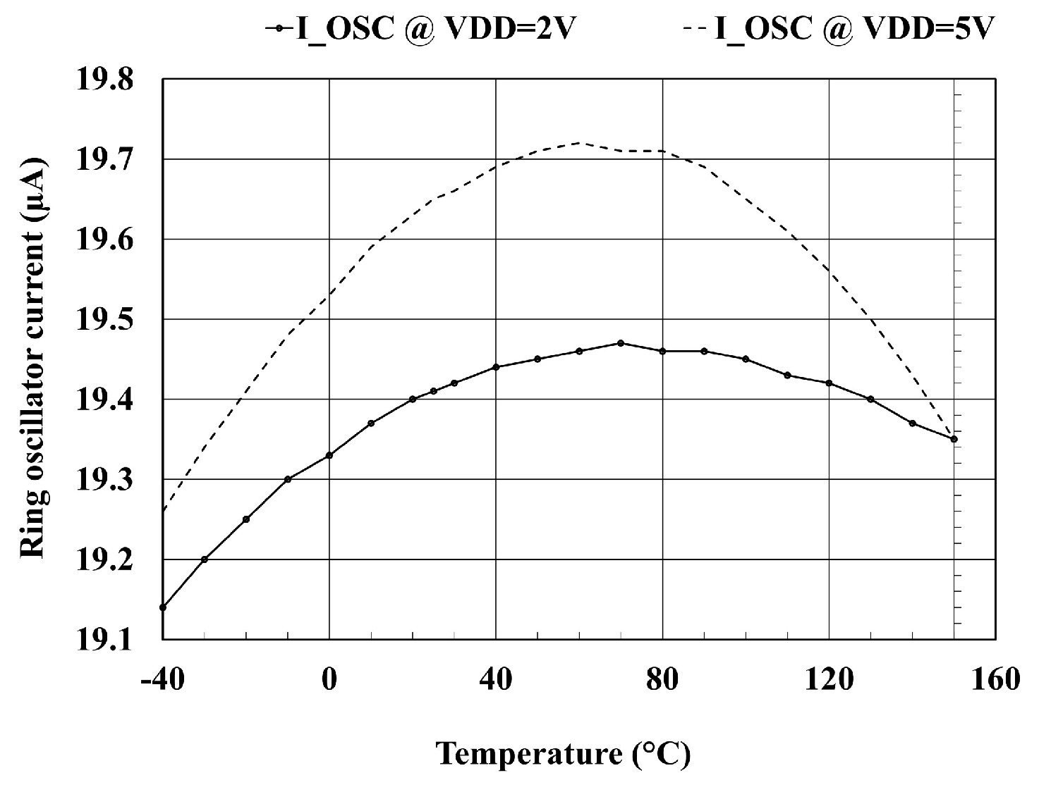
3. Simulations and Results

3.1. Schematic Level Simulations

In this subchapter, schematic level simulations were performed in the Cadence Virtuoso environment work system using a 250 nm CMOS technology. Figure 5 shows the internal constant voltage V D D _ I N T change with temperature. The curvature determined by the bandgap voltage characteristic can be observed. For the 2 V supply voltage, a waveform flattening occurs due to the very small difference between V D D and V D D _ I N T . This will determine the low−dropout circuit output stage ( M 5 transistor) to work in the linear region. This will lead to a smaller fluctuation in the internal constant voltage even with the process and mismatch.
The typical minimum and maximum V D D _ I N T potentials reached for each simulated supply voltage were 1.99 V with 1.995 V for V D D = 2   V and 2.001 V with 2.043 V for V D D = 5   V . These numbers show that a 2 V voltage source compensated with V D D and temperature was achieved.
The frequency dependency given by supply voltage is illustrated in Figure 6. In the first one (a), the basic ring oscillator is implemented, with the internal supply voltage and the current−starved disconnected from the circuit. As expected, the PLL dependency on supply voltage is almost linear, the minimum and maximum values being 119.4 MHz ( V D D = 2   V ) and 387.6 MHz ( V D D = 5   V ). This high−frequency range is unacceptable for applications where precision is critical.
In the second picture (b), the current−starved ring oscillator is designed and simulated. The frequency range is considerably decreased compared to (a), with a minimum frequency reached at 2 V (40.43 MHz) and a peak value around 2.6 V (53 MHz). The third one (c) uses both the current−starved architecture and the internal supply voltage generated by the LDO. The frequency range is tighter (40.25 MHz; 42.45 MHz); thus, the frequency stability when V D D changes is improved. A decrease in frequency can be observed when the supply voltage exceeds 4 V, with a local minimum value of 41.45 MHz being reached.
The fourth picture (d) highlights the results obtained using the proposed PLL circuit described in this paper. The cascaded current−starved improves the frequency variation at the start and the end of the graph, reducing the current variation given by the fluctuation of the internal supply voltage; thus, the difference between the maximum and minimum value is only 0.53 MHz, a 1.67 MHz improvement compared to (c). Furthermore, using cascaded current−starved mirrors, the temperature effects over time are minimized due to the mirror drain−source voltage being equal and the dependency given by the short channel effect being discarded. Hence, the same current flows through all inverters and capacitors in the ring oscillator.
Figure 7a reports the time response at room temperature after the level shifter for the clock signal, considering two supply voltages: 2 V and 5 V. To better understand the results obtained, zoom is made on the x−axis.
The two waveforms’ duty cycle is approximately 50%. This means that, in a charge pump architecture, by using the designed oscillator in this paper, the capacitor’s charge and discharge time will be equal and the output ripple reduced.
The oscillator frequencies obtained at room temperature for the two supply voltages mentioned above are 50.01 MHz ( V D D = 2   V ) and 50.04 MHz ( V D D = 5   V ), close to the 50 MHz desired value.
Figure 7b illustrates the frequency variation in a typical corner with temperature for the same supply voltages. The constant current and the potentials are derived from a circuit that uses bandgap voltage theory [16]. The same curvature with temperature for the clock frequency is obtained. Typical peak values of 50.1 MHz (for V D D = 2   V ) and 50.15 MHz (for V D D = 5   V ) are recorded around 60 °C, while the minimum value (49.2 MHz) was reached for 5 V supply voltage at 150 °C. The temperature percentage error ε o s c obtained using the formula below is 1.6.
ε o s c = S v a l T v a l T v a l 100
where S v a l represents the experimental value and T v a l the theoretical one.
Process variations can affect the oscillator frequency compensation with temperature and power supply. To evaluate the circuit performance considering this aspect, slow and fast corner simulations are performed. In the slow corner (Figure 8a), the transistors threshold point is shifted to a higher value; thus, a greater VGS voltage is required to turn the devices on.
A decreased center frequency value of around 38.3 MHz (for V D D = 2   V ) and 38.5 MHz (for V D D = 5   V ) was obtained due to the lower constant current generated in this corner. In the fast corner (Figure 8b), the transistor’s threshold point is shifted to a lower value, leading to the decreased VGS voltage needed to turn the devices on. An increased average frequency value of around 64.1 MHz (for V D D = 2   V ) and 63.9 MHz (for V D D = 5   V ) is obtained. Compensation with temperature and power supply is achieved even in these corners, representing the worst process variation scenarios. To further reduce the curvature, second−order compensation for the bandgap circuit has to be implemented.
The average current consumed by the designed ring oscillator doesn’t exceed 20 µA regardless of supply voltage, as seen in Figure 9. The entire circuit that includes all the functional architecture blocks requires less than 125 µA.
Figure 10a shows the results obtained using the Monte Carlo sampling technique for the clock signal at two supply voltages. The means and standard deviations are 49.84 MHz and 2.019 MHz for V D D = 2   V , respectively 49.87 MHz and 2.023 MHz for V D D = 5   V . The numbers show that even if the mismatch influences the oscillator frequency, the variation given by the change in supply voltages is negligible.
Figure 10b presents, at room temperature, the Monte Carlo simulation results over the total current consumed by the proposed ring oscillator for the same supply voltages as mentioned above. The means and standard deviations are 19.35 µA and 0.6 µA for V D D = 2   V , respectively 19.6 µA and 0.7 µA for V D D = 5   V . The maximum current is listed in Table 3.
The outcome of the schematic level simulations proves that the suggested design is suitable for applications that require low power consumption [17]. A summary of the results obtained from the architecture is presented in Table 3 and Table 4.

3.2. Post Layout Simulations

Parasitic effects can influence the oscillator frequency compensation with temperature and power supply. To evaluate the circuit performance, post−layout simulations were performed using the parasitic extraction method. The results are presented in Figure 11.
The frequency dependency given by supply voltage is illustrated in Figure 11a. A center frequency value of around 48.9 MHz is obtained. Peak and minimum values with parasitic extraction are 49.07 MHz and 48.6 MHz. Figure 11b shows the typical temperature influence over the proposed ring oscillator technique at two supply voltages. Peak and minimum values are 48.83 MHz, 48.14 MHz (for V D D = 2   V ) and 48.95 MHz, 48.06 MHz (for V D D = 5   V ). The temperature percentage error with PEX is 1.71, comparable to that accomplished from schematic level simulations. These values confirm that temperature and supply voltage compensation are achieved despite parasitic effects.
Table 5 lists ring VCO architectures performance obtained with parasitic effects compared to previously reported works in the literature. The proposed technique performed better than [7,18,19,20] in terms of power consumption, die area, and temperature range and was close to [7] regarding frequency variation with temperature.

4. Layout Implementation

The circuit layout is presented in Figure 12. For the floorplan, the main goal was to isolate the ring oscillator digital gates as far as possible from the rest of the circuit to reduce the wire’s parasitic capacitance. The ring oscillator digital block and the no−overlap schematic were placed on the layout’s upper side, close to each other, to achieve short clock wires. Because no standardized digital cells were used in the schematic, all the digital blocks were designed to obtain minimum interconnect capacitances and resistances [21].
The capacitors were placed over the circuit analogic part to improve the die area. Capacitors used were MIM type and made of upper metal layers, M3 and M4, to reduce parasitic elements. The clock wires were drawn on a higher metal to reduce vertical capacitances even more. The no−overlap block was designed with full symmetry to match the possible delays on the signal path.
For the LDO and the current mirrors in the ring oscillator, a common−centroid matching with two axes of symmetry was used [22]. For the current mirrors in the ring oscillator, dummies were used to achieve the rows and columns number with minimum distance between transistors for better matching and minimum wires above each row. The interconnects mostly used M1 (red) and M2 (pink), M1 for vertical interconnects, and M2 for horizontal ones. M2 was used for routing over transistors instead of a superior metal due to capacitors and to reduce cost. For the differential pair, cross−coupled matching was used. The last layout part was implemented to achieve the wire’s full symmetry (according to the current flow) and was placed in the middle for better isolation. Multiple contact guard rings were used around all blocks to reduce susceptibility to latch−up. All resistors were placed together (green color), with minimum distance between them to reduce possible etching errors. LVS and DRC verifications were done to check for design errors. The circuit layout die area was 0.023 mm2.

5. Conclusions

This paper focused on designing a clock circuit, compensated with temperature and power supply, maintaining these performances even when process variations occur, starting from a ring oscillator as the architecture core. Simulations were performed using 250 nm CMOS technology. A pre−layout 50 MHz center frequency at 25 °C with a 1.6 temperature percentage error was achieved. Cascade current mirrors, together with a constant current as a reference, were used to reduce the circuit’s total power consumption along with temperature variation. At room temperature, the maximum current required for the ring oscillator was 24 µA, and the architecture’s overall maximum current was 125 µA. A low−dropout block ensured a regular period with a change in the supply voltage. The generated signal rebounded to V D D using a level shifter. The logic gate’s threshold point was established at half of the supply voltage to provide a 50% duty cycle. Post−layout simulations to account for parasitic effects were performed to confirm temperature and supply voltage compensation was achieved even with parasitic effects. A 48.9 MHz center frequency was reached in this case. Performance comparison of the designed PLL with previously reported clock circuits in the CMOS process was also concluded.
These results highlight the fact that the proposed circuit can be used in charge pump architectures to implement the operational amplifier’s rail−to−rail input stage.

Author Contributions

Conceptualization, C.S., A.N., O.P., D.D. and L.D.; methodology, C.S. and L.D.; software, C.S. and O.P.; validation, C.S., A.N. and L.D.; formal analysis, C.S.; investigation, C.S.; resources C.S.; data curation, C.S.; writing—original draft preparation, C.S. and A.N.; writing—review and editing, C.S., D.D. and L.D.; visualization. C.S., D.D. and L.D.; supervision, L.D. and D.D.; project administration, L.D.; funding acquisition, L.D. and D.D. All authors have read and agreed to the published version of the manuscript.

Funding

This paper publication is funded by the University Politehnica of Bucharest, PUBART project.

Conflicts of Interest

The authors declare no conflict of interest.

References

  1. Butkovic, Z.; Szabo, A. Analysis of the CMOS differential amplifier with active load and single−ended output. In Proceedings of the 12th IEEE Mediterranean Electrotechnical Conference (IEEE Cat. No.04CH37521), Dubrovnik, Croatia, 12–15 May 2004; Volume 1, pp. 417–420. [Google Scholar] [CrossRef]
  2. Veselu, A.C.; Stănescu, C.; Brezeanu, G. Low Current Constant−gm Technique for Rail−to−Rail Operational Amplifiers. In Proceedings of the 2020 International Semiconductor Conference (CAS), Sinaia, Romania, 7–9 October 2020; pp. 253–256. [Google Scholar] [CrossRef]
  3. Ballo, A.; Grasso, A.D.; Palumbo, G. Dickson Charge Pump: Design Strategy for Optimum Efficiency. In Proceedings of the 2021 19th IEEE International New Circuits and Systems Conference (NEWCAS), Toulon, France, 13–16 June 2021; pp. 1–4. [Google Scholar] [CrossRef]
  4. Ballo, A.; Grasso, A.D.; Palumbo, G. The Dickson Charge Pump as a Signal Amplifier. IEEE Trans. Circuits Syst. I Regul. Pap. 2022, 69, 3476–3489. [Google Scholar] [CrossRef]
  5. Chiang, Y.H.; Liu, S.I. A Submicrowatt 1.1−MHz CMOS Relaxation Oscillator With Temperature Compensation. IEEE Trans. Circuits Syst. II Express Briefs 2013, 60, 837–841. [Google Scholar] [CrossRef]
  6. Li, Q.; Tong, X. A Multifunction Relaxation Oscillator with Area and Power Consumption Reduced. In Proceedings of the 2020 IEEE 3rd International Conference on Electronics Technology (ICET), Chengdu, China, 8–11 May 2020; pp. 228–232. [Google Scholar] [CrossRef]
  7. Sundaresan, K.; Allen, P.E.; Ayazi, F. Process and temperature compensation in a 7−MHz CMOS clock oscillator. IEEE J. Solid−State Circuits 2006, 41, 433–442. [Google Scholar] [CrossRef]
  8. Ballo, A.; Pennisi, S.; Scotti, G.; Venezia, C. A 0.5 V Sub−Threshold CMOS Current−Controlled Ring Oscillator for IoT and Implantable Devices. J. Low Power Electron. Appl. 2022, 12, 16. [Google Scholar] [CrossRef]
  9. Corres−Matamoros, A.; Martínez−Guerrero, E.; Rayas−Sanchez, J.E. A programmable CMOS voltage controlled ring oscillator for radio−frequency diathermy on−chip circuit. In Proceedings of the 2017 International Caribbean Conference on Devices, Circuits and Systems (ICCDCS), Cozumel, Mexico, 5–7 June 2017; pp. 65–68. [Google Scholar]
  10. Saurab, B.; Chavan, A.P. Ultra−Low Power, Area Efficient and High−Speed Voltage Level Shifter based on Wilson Current Mirror. In Proceedings of the 2021 IEEE Mysore Sub Section International Conference (MysuruCon), Karnataka, India, 24–25 October 2021; pp. 108–113. [Google Scholar] [CrossRef]
  11. Tianwang, L.; Jiang, J.; Bo, Y.; Xingcheng, H. Ultra low voltage, wide tuning range voltage controlled ring oscillator. In Proceedings of the 2011 9th IEEE International Conference on ASIC, Xiamen, China, 25–28 October 2011; pp. 824–827. [Google Scholar]
  12. Xie, L. Two−stage operational amplifier with Class A and B output stage. In Proceedings of the 2021 3rd International Academic Exchange Conference on Science and Technology Innovation (IAECST), Guangzhou, China, 10–12 December 2021; pp. 260–263. [Google Scholar] [CrossRef]
  13. Ballo, A.; Pennisi, S.; Scotti, G. 0.5 V CMOS Inverter−Based Transconductance Amplifier with Quiescent Current Control. J. Low Power Electron. Appl. 2021, 11, 37. [Google Scholar] [CrossRef]
  14. Tan, M.; Zhou, Q. A two−stage amplifier with active miller compensation. In Proceedings of the 2011 IEEE International Conference on Anti−Counterfeiting, Security and Identification, Xiamen, China, 24–26 June 2011; pp. 201–204. [Google Scholar] [CrossRef]
  15. Stancu, C.; Dobrescu, D.; Dobrescu, L. Offset Voltage Reduction Methods for a Two−Stage Folded Cascode Operational Amplifier. In Proceedings of the 2022 14th International Conference on Electronics, Computers and Artificial Intelligence (ECAI), Ploiesti, Romania, 30 June–1 July 2022; pp. 1–4. [Google Scholar] [CrossRef]
  16. Banba, H.; Shiga, H.; Umezawa, A.; Miyaba, T.; Tanzawa, T.; Atsumi, S.; Sakui, K. A CMOS bandgap reference circuit with sub−1−V operation. IEEE J. Solid−State Circuits 1999, 34, 670–674. [Google Scholar] [CrossRef] [Green Version]
  17. Nayak, R.; Kianpoor, I.; Bahubalindruni, P.G. Low power ring oscillator for IoT applications. Analog. Integr. Circuits Signal Process. 2017, 93, 257–263. [Google Scholar] [CrossRef]
  18. Hamman, H.H.; Hassan, K.M.; Ibrahim, S.A. An Ultra−Low−Power Process−and− Temperature Compensated Ring Oscillator. In Proceedings of the 2022 9th International Conference on Electrical and Electronics Engineering (ICEEE), Alanya, Turkey, 29–31 March 2022; pp. 1–5. [Google Scholar] [CrossRef]
  19. Lakshmikumar, K.R.; Mukundagiri, V.; Gierkink, S.L.J. A Process and Temperature Compensated Two−Stage Ring Oscillator. In Proceedings of the 2007 IEEE Custom Integrated Circuits Conference, San Jose, CA, USA, 16–19 September 2007; pp. 691–694. [Google Scholar] [CrossRef]
  20. Leung, K.; Lo, C.; Mok, P.; Mai, Y.; Leung, W.; Chan, M. Temperature−compensated CMOS ring oscillator for power−management circuits. Electron. Lett. 2007, 43, 786–787. [Google Scholar] [CrossRef]
  21. Jacob Baker, R. CMOS Circuit Design, Layout, and Simulation, 3rd ed.; John Wiley & Sons, Inc.: Hoboken, NJ, USA, 2010. [Google Scholar]
  22. Hastings, A. The Art of Analog Layout, 1st ed.; Prentice Hall: Hoboken, NJ, USA, 2001. [Google Scholar]
Figure 1. Proposed clock circuit block diagram with ring oscillator.
Electronics 12 00507 g001
Figure 2. Classical current−starved ring VCO.
Electronics 12 00507 g002
Figure 3. Proposed design architecture for the ring oscillator circuit.
Electronics 12 00507 g003
Figure 4. Low−dropout regulator schematic.
Electronics 12 00507 g004
Figure 5. Constant internal supply voltage adjustment with temperature.
Electronics 12 00507 g005
Figure 6. Frequency dependency given by supply voltage for the ring oscillator. (a) Basic implementation; (b) Current−starved added; (c) Internal supply voltage and current−starved connected; (d) Proposed design with cascaded current−starved.
Electronics 12 00507 g006
Figure 7. Typical simulation results for the clock circuit. (a) Time response; (b) Frequency variation with temperature and VDD.
Electronics 12 00507 g007
Figure 8. Frequency variation with temperature and VDD in corners. (a) Slow; (b) Fast.
Electronics 12 00507 g008
Figure 9. Ring oscillator quiescent current variation with temperature and VDD.
Electronics 12 00507 g009
Figure 10. Monte Carlo simulations histograms. (a) Oscillation frequency; (b) ring oscillator consumed current.
Electronics 12 00507 g010
Figure 11. Frequency characteristics with PEX simulations. (a) vs. supply voltage; (b) vs. temperature.
Electronics 12 00507 g011
Figure 12. Circuit layout. (a) including M3 and M4 masks; (b) without MIM capacitors.
Electronics 12 00507 g012
Table 1. Design parameters for ring oscillator.
ParameterValue
R1, R2350 kΩ, 300 kΩ
C1−C432.8 fF
(W/L) M1–M3, M5–M7–M9–M11–M136/3, 18/3 µm/µm
(W/L) M2–M4, M6–M8–M10–M12–M144/2, 12/2 µm/µm
(W/L) M15, M17–M19–M21–M23–M2522/4, 66/4 µm/µm
(W/L) M16, M18–M20–M22–M24–M2618/3, 54/3 µm/µm
Table 2. Design parameters for LDO.
ParameterValue
R1, R2, R3, R4200 kΩ, 200 kΩ, 600 kΩ, 28.9 kΩ
C1, C21.15 pF, 11.5 pF
(W/L) M1–M220/2 µm/µm
(W/L) M3–M4, M580/0.5, 160/0.5 µm/µm
(W/L) M6–M7, M8–M912/2, 60/2 µm/µm
Table 3. Results summary for 2 V supply voltage.
ParameterTypical Value @ 25 °CMonte Carlo (Mean ± 6 σ) @ 25 °CMin. and Max. Typ. Values over Temperature
Clock frequency (MHz)50.01(37.72; 61.98)(49.3; 50.1)
IQ ring oscillator (µA)19.34<22.95(19.1; 19.38)
IQ total (µA)62.24<75(60.14; 64.69)
VDD_INT (V)1.994(1.966; 2.019)(1.99; 1.995)
Table 4. Results summary for 5 V supply voltage.
ParameterTypical Value @ 25 °CMonte Carlo (Mean ± 6 σ) @ 25 °CMin. and Max. Typ. Values over Temperature
Clock frequency (MHz)50.04(37.73; 62)(49.2; 50.15)
IQ ring oscillator (µA)19.65<24(19.34; 19.72)
IQ total (µA)103.2<125(98.52; 107.9)
VDD_INT (V)2.043(1.84; 2.23)(2.001; 2.043)
Table 5. Comparison results with previously reported work.
Parameter[7][18][19][20]This Work
Technology (nm)250180130250250
Supply voltage (V)2.21.83.332
Power consumption (mW) @ Center frequency1.50.43719.8N/A0.124
Center frequency (MHz)71001250148.9
Frequency variation (with temperature) (%)0.844.494.83.331.71
Die Area (mm2)1.6N/A201620.023
Temperature range−40 °C–125 °C−40 °C–125 °C−40 °C–120 °C−40 °C–125 °C−40 °C–150 °C
Disclaimer/Publisher’s Note: The statements, opinions and data contained in all publications are solely those of the individual author(s) and contributor(s) and not of MDPI and/or the editor(s). MDPI and/or the editor(s) disclaim responsibility for any injury to people or property resulting from any ideas, methods, instructions or products referred to in the content.

