Article

Procedural- and Reinforcement-Learning-Based Automation Methods for Analog Integrated Circuit Sizing in the Electrical Design Space

1
Electronics & Drives, Reutlingen University, 72762 Reutlingen, Germany
2
Cognitive Systems, Reutlingen University, 72762 Reutlingen, Germany
*
Author to whom correspondence should be addressed.
Electronics 2023, 12(2), 302; https://doi.org/10.3390/electronics12020302
Submission received: 29 November 2022 / Revised: 23 December 2022 / Accepted: 25 December 2022 / Published: 6 January 2023

Abstract

:
Analog integrated circuit sizing is notoriously difficult to automate due to its complexity and scale; thus, it continues to heavily rely on human expert knowledge. This work presents a machine learning-based design automation methodology comprising pre-defined building blocks such as current mirrors or differential pairs and pre-computed look-up tables for electrical characteristics of primitive devices. Modeling the behavior of primitive devices around the operating point with neural networks combines the speed of equation-based methods with the accuracy of simulation-based approaches and, thereby, brings quality of life improvements for analog circuit designers using the g m / I d method. Extending this procedural automation method for human design experts, we present a fully autonomous sizing approach. Related work shows that the convergence properties of conventional optimization approaches improve significantly when acting in the electrical domain instead of the geometrical domain. We, therefore, formulate the circuit sizing task as a sequential decision-making problem in the alternative electrical design space. Our automation approach is based entirely on reinforcement learning, whereby abstract agents learn efficient design space navigation through interaction and without expert guidance. These agents’ learning behavior and performance are evaluated on circuits of varying complexity and different technologies, showing both the feasibility and portability of the work presented here.

1. Introduction

As a motivation and introduction, the current state of analog integrated circuit (IC) sizing automation, including the approaches relevant to this work, is outlined in the following subsections. Furthermore, comparisons are drawn between related work regarding machine learning (ML) and reinforcement learning (RL) in the field, further detailing the differences to the approach presented here.

1.1. Current State of Analog IC Sizing Automation

Despite comprehensive research regarding the design automation of analog Mixed-Signal ICs, in terms of topology synthesis [1], design optimization [2], or yield optimization [3], this domain has still not caught up with its digital counterpart [4]. As such, it remains a predominantly manual task relying heavily on human expert knowledge due to the complexity of the subject matter. While digital circuits are designed from a higher level, the gate level, due to their time- and value-discrete nature, analog circuit designers are still sizing individual transistors by hand, bottlenecking the rest of the design flow. Existing automation approaches are categorized as either optimization-based or knowledge-based.
The former employs optimization algorithms, such as Bayesian optimization (BO) [5] or evolutionary strategies (ESs) [6], for example, to find new solutions. Depending on the algorithm and complexity of the circuit, this may lead to long execution times, be sample inefficient, or return physically infeasible solutions [7].
The latter requires human experts to express their knowledge in an executable format, reproducing the results they have found previously [8]. Some overhead is associated with each new design, but value is accrued with each reuse. This is mainly based on the g m / I d method [9] and the corresponding pre-computed look-up tables (LUTs), which combines the accuracy of simulation-based methods with the execution time of equation-based methods [10].

1.2. Procedural Analog IC Sizing

The main drawback is a lacking higher level of abstraction. Considering the continuous nature of analog signals, all physical effects and parasitics have to be considered during the design of analog integrated circuits. Hence, they are still designed on the transistor level, in contrast to a fixed set of gates in the digital domain, making it difficult for optimization-based automation approaches [7,11] to find solutions within such a high-dimensional design space in an adequate time.
Formalizing the expert knowledge necessary for the design of analog circuits lays the foundation for procedural automation approaches, which have been successfully employed in the layout domain in the past [12]. These procedures are able to generate layouts for commonly used analog circuits such as current mirrors or differential pairs. These frequently reoccurring structures have been deemed “building blocks” [13,14]. While it is possible to implement such generators for more complex, less frequently used circuits, the time investment is a considerable trade-off. Recently, similar approaches have made advances in the circuit design domain as well [15].

1.3. Machine Learning for EDA

Consequently, learning-based approaches have been emerging in recent years [16,17], attempting to address the yet-unresolved challenges surrounding analog IC design automation by means of ML and RL.
Both, neural networks (NNs) and deep learning (DL) have shown great potential in a wide range of tasks [18]. In the field of computer vision especially, convolutional neural networks (CNNs) enable the autonomous extraction of meaningful information from images, e.g., for object detection [19], semantic segmentation [20], or 2D/3D human pose estimation [21], to only name a few. In recent years, the interest in the application of DL for electronic design automation (EDA) has also increased [17,22], and methods for analog circuit sizing are an active research topic.
While it has been shown that the behavior of primitive devices can be modeled with NNs [23,24], this paper attempts to extend this approach to the building block [13] level. Considering the universal approximation theorem [25], NNs are able to map characteristics of such a building block to corresponding sizing parameters, e.g., W / L ratios, given sufficient data.
Kahraman and Yildirim [26] showed that they can size a current mirror and a differential amplifier with the help of NNs, i.e., a multilayer perceptron (MLP) and a general regression NN. The networks learn a mapping from the performance parameters to the devices’ widths, while the lengths are kept constant.
Mendhurwar et al. [27] proposed a more general NN-based framework for circuit sizing. They obtained a large database of simulation data by performing parameter sweeps over primitive device models for different technologies and used these data for training NNs. Due to difficulties in fitting a single model to the large parameter spaces, Mendhurwar et al. used a binning algorithm to split the parameter space and train multiple sub-models on the resulting bins. Additional correction models were applied to further improve accuracy in specific failure cases.
A combination of an evolutionary algorithm and an NN was proposed by Islamoglu et al. [28]. When evaluating the performance of the individuals, the simulation results were not discarded, but used for training an NN that learns to predict the performances of individuals. The better this network is able to predict the performances, the less simulation runs are required, resulting in a reduction of the execution time by up to 64.80%.

1.4. Reinforcement Learning for EDA

Reinforcement learning is a framework for finding optimal behavior in sequential decision-making problems through interaction. The emergence of deep-learning- based function approximation and subsequently deep reinforcement learning (DRL) has led to tremendous successes in several challenging control problems, from board and video games [29,30] to autonomous driving [31] and robotics [32,33]. By virtue of its two simple provisions, (1) that the problem can be formulated as an Markov decision process (MDP) and (2) that there exists a measure of reward, which indicates the desirability of a given interaction, the framework can be applied to solve an even wider variety of tasks.
With AutoCkt, Settaluri et al. [34] applied DRL to the analog circuit sizing problem. Given a netlist, a test bench, and a target specification, AutoCkt can generate trajectories of actions, e.g., incrementing or decrementing transistor widths, thus satisfying the desired target specification. The actions the RL agent is allowed to take are restricted to specific intervals and step sizes, transforming a continuous action space into a discrete one. AutoCkt uses the algorithm proximal policy optimization (PPO) [35], which is a popular baseline because of its ability to handle large and continuous action spaces, as well as its relative robustness during learning. However, as an on-policy method, PPO discards sampled interactions after a single round of updates—a severe hindrance in a regime where sampling interactions are expensive, e.g., because of slow simulations. For reference, PPO can solve simple continuous control problems after a few tens to hundreds of thousands of interactions, usually sampled at thousands of frames per second, a sampling rate about two orders of magnitude higher than running the 25 m s simulation used by Settaluri et al.
Wang et al. leveraged the graph structure of circuits and presented a graph convolutional network (GCN)-based RL circuit designer [36], which operates in continuous action spaces, such as the widths and lengths of transistors. Training is performed with the deep deterministic policy gradient (DDPG) [37] algorithm, a natural choice as DDPG is an off-policy actor–critic algorithm with the ability to sample interactions from a large memory buffer repeatedly, only discarding them after the buffer is overflowing. As a reward, the authors defined a figure of merit (FOM): the weighted sum of the normalized performance metrics, i.e., the distance between the target and actual performance—a technique known as reward shaping [38], which provides a dense reward signal, which, in some cases, can aid learning. GCN-RL is run for 10 4 steps corresponding to a runtime of around 5 h and, thus, 1.8   s per step. The time required per step is consistent with our approach, which is around 2 s per step.
Li et al. introduced a stochastic attention-based graph neural network (GNN) called circuit attention network (CAN) [39]. They followed the FOM definition of [36], but treated the normalized metrics as a random variable optimized for small variance. This leads to the preference of sizings with small performance variance induced by the layout.
Noting these prior works, we highlight the importance of sensible decisions concerning the definition of the analog sizing problem as an MDP and the choice of RL algorithms. Like Wang et al., we built our approach upon an off-policy algorithm, namely twin delayed deep deterministic policy gradient (TD3) [40], the successor to DDPG. TD3 attempts to alleviate several shortcomings of its predecessor, such as an overestimation bias in the value function leading to the agent getting stuck in local optima and, thus, not genuinely solving complex tasks with small solution spaces. Further, we employed hindsight experience replay (HER) [41], an augmented memory buffer designed to support learning in sparse reward regimes. The sizing task is only solved once all target specifications are met simultaneously, and successful episodes are rare in the agent’s initial exploration. HER effectively “moves the goalpost” when sampling episodes from the memory buffer; while the agent may not have reached the target specification, it has met a target specification. Thus, the agent learns to navigate the state (performance parameter) space effectively, making the most of a limited number of simulation interactions without the need for manual reward shaping.
Lastly, unlike previous works conducted purely in geometrical spaces, we propose to transfer the sizing problem into the electrical parameter space, significantly reducing the search space [42]. This paradigm shift outright prevents dead-end episodes due to infeasible configurations of geometrical parameters by only allowing primitive devices at sensible operating points, which in turn guarantees computable results from the simulation analyses.
This lines up with the preferred g m / I d methodology [43] for manual design by human experts. Device geometries are merely a means to an end, while the electrical characteristics of individual devices are much more closely correlated with the overall circuit performance. It is generally difficult for human experts to intuitively relate transistor dimensions to circuit performance. Instead, they have a better sense of what the operating points of specific devices should be.

1.5. Structure

Section 2 introduces the concept of function mappings from the electrical design domain to geometrical sizing. Subsequently, the sampling of data and training are covered in Section 3. The trained models are then used in Section 4 to demonstrate the procedural design with an ML-powered g m / I d methodology. This methodology for analog IC sizing automation was first reported in [44]. Section 5 describes how these function mappings are used in conjunction with RL agents, where they act as a performant interface to the g m / I d methodology. Experimental results of this approach, which were first presented in [45], are recapped and discussed in Section 6.

2. Function Mappings for Circuit Sizing

First, let us consider a very simple design task, such as a voltage divider, made up only of resistors. Here, a designer would start by determining the required resistances, which are the values of the electrical ( E ) domain, independent of any particular technology. In a subsequent step, the designer would pick a specific resistor model from a given process design kit (PDK) and convert the resistances to corresponding geometrical ( G ) values according to the documentation. This voltage divider will behave the same in any technology, provided there is a way of converting the desired resistance ( E ) to the correct widths and lengths ( G ).
When sizing transistors, however, designers do not have this luxury of specifying desired electrical behavior and looking up a conversion into geometrical sizing parameters in the PDK manual. While the equations mapping terminal voltages and geometries to operating point parameters exist in the device models [46,47], they are not easily rearranged and only grow in complexity with each new version. As such, this would require function optimization with a simulator in the loop to find geometrical parameters that result in the desired electrical behavior. The search space, spanned by possible combinations of widths and lengths for multiple devices in a circuit, is considerable and difficult to constrain. It would be much more intuitive for a circuit designer, however, to constrain the parameters of the electrical domain, such as the speed ( f ug ) or the efficiency ( g m / i d ) of a device. In many cases it is possible to fix such an electric parameter to a specific value, greatly reducing the search space. A technology-dependent way of translating desired operating point parameters into widths and lengths would lift the design problem into the electrical domain. Here, the task can be viewed as entirely decoupled from the technology and geometries. Once a design point, consisting of the desired electrical behavior of the transistors, is found, it is the responsibility of such a translation function for a given technology to produce the correct widths and lengths, resulting in this specified electrical behavior. That way, the same operating point can be reproduced, provided the function exists for a PDK. If the electrical behavior of individual devices is reproduced, the performance of the overall circuit should be comparable as well.
Instead of analytically inverting the equations of the transistor model, in this approach, non-linear regression models are trained to learn and approximate the mappings shown in (1).
ρ type , tech : g m I d f ug V ds V bs I d W L g ds W V gs (
This results in the translation function ρ for a given PDK (tech) and device type, where this type is either NMOS or PMOS. As for the inputs to this model, the aforementioned speed and efficiency are considered expert knowledge because an experienced circuit designer has an intuition for choosing these values. Additionally, some prior knowledge in the form of the drain–source voltage ( V ds ) and bulk–source voltage ( V bs ) is used as part of the input. These latter parameters can be determined by the location of the device in the circuit.
Related work [13] shows that the design space can be reduced even further by breaking a circuit into building blocks, such as the current mirror or the differential pair, which are highlighted in Figure A1. While NNs can be trained to approximate a mapping from building block specific performances to individual sizing parameters for each device therein [26], this work focuses on an alternative approach. It is shown that sizing a single reference device and simply propagating the sizing parameters to related devices within a building block is sufficient [48]. This only requires training data for a single device and implicitly ensures that functionally related devices are matched. Hence, the sizing of a building block is reduced to a single NN evaluation, which will be elaborated on during the example in Section 4.

3. Data Sampling and Training

As mentioned previously, in Section 2, the foundation for this approach is LUTs containing the operating point parameters of a transistor [9]. NNs can be trained to learn a mapping of this data, approximating the simulation model. However, previous work has shown that it can be difficult for NN predictions to converge over the entire input space [27]. Instead of binning the input space and training a correction model, in this approach, the dataset is sampled [49] and transformed [50], changing the distribution of the outputs, as shown in Figure 1, yielding better convergence of a single model.
All mappings modeling primitive device behavior around the operating point presented in this work were trained using the same network architecture and training algorithm, which was found by iteratively extending the architectures of previous works [26,27]. The result is an NN with 4 inputs, 7 fully connected hidden layers, and 4 outputs, where rectified linear unit (ReLU) [51] is used as the activation for all hidden layers. These hidden layers consist of 128, 256, 512, 1024, 512, 256, and 128 neurons, respectively. The Adam optimizer [52], with a learning rate of α = 10 3 and exponential decay rates for the moment estimates β 1 = 0.9 and β 2 = 0.999 , is used to minimize the mean-squared error (MSE) between the LUT and predictions. Additionally, the mean absolute error (MAE) is calculated for the validation set while monitoring the training progress. Training on a dataset of 4 × 10 6  samples for 24 epochs with a batch size of 128 took ca. 35 min on an NVIDIA® RTX  3090. Figure 2 shows how well the predictions agree with the LUT after training. The left shows the drain current density ( J d = I d / W ) over the efficiency, while the self-gain ( g m / g ds ) over the saturation voltage ( v dsat ) is depicted on the right.
The training data were obtained by characterizing primitive devices over a range of terminal voltages ( V ds , V ds , V ds ) and geometries (W, L), resulting in two ML models (NMOS and PMOS) per PDK.

4. Procedural Design Example

For demonstrating the viability of the methodology for human circuit designers, the symmetrical amplifier (SYM) shown in Figure A1a is sized to meet the specification given in Table 1. The strategy is expressed entirely in the electrical domain as a sequence of function evaluations for each building block in the circuit. When executing this procedure for a technology, the correspondingly trained models act as a drop-in replacement for ρ .
Initially, prior knowledge is considered by observing the specification, given in Table 1, and deciding on a biasing current I d , MNCM 12 = I B 1 = 2 × I B 0 , as well as an output current I d , MNCM 32 = I B 2 = 4 × I B 0 , resulting in the ratio M = 1 : 4 of the PMOS current mirrors MPCM2. Usually, this is chosen to balance the power consumption and phase margin. Since this has to be analyzed separately by simulation, starting values M cm 21 = 1 and M cm 22 = 4 were selected. Thus, a sizing strategy is expressed as a sequence of function evaluations, where the inputs depend on the knowledge and intuition of an expert circuit designer and on prior knowledge of the location and connectivity of the device in the circuit. This procedure, which is reminiscent of the manual work flow with analytical equations, is illustrated in detail hereafter and captured in executable form. First, since the common mode output voltage V out , cm is known, current mirror MNCM3 is considered with (2).
ρ NMOS ( g m / I d ) cm 3 f ug , cm 3 0.5 · V DD 0.0 J d , cm 3 L cm 3 g ds , cm 3 / W cm 3 V gs , cm 3
This defines the length L cm 3 and width W cm 3 = I B 2 / J d , cm 32 in terms of speed and efficiency and constitutes M cm 31 = M cm 32 = 2 for a 1 : 1 ratio. Next, the active load current mirrors MPCM21 and MPCM22 are considered with the single model evaluation given in (3), thereby sizing them identically in terms of the same f ug and g m / I d .
ρ PMOS ( g m / I d ) cm 2 f ug , cm 2 V DD V out , cm 0.0 J d , cm 2 L cm 2 g ds , cm 2 / W cm 2 V gs , cm 2
yielding the length L cm 2 and the width W cm 2 = ( I B 1 / 2 ) / J d , cm 22 , while the ratio M cm 21 : M cm 22 was defined earlier. Let V y = V DD V gs , cm 2 , then the differential pair MND1 is defined in terms of speed and efficiency with (4).
ρ NMOS ( g m / I d ) dp 1 f ug , dp 1 V y V CM V CM J d , dp 1 L dp 1 g ds , dp 1 / W dp 1 V gs , dp 1
where the width and length are obtained in the same way as previously described. Finally, (5) defines the sizing for MNCM1 in terms of electrical parameters.
ρ NMOS ( g m / I d ) cm 1 f ug , cm 1 V CM 0.0 J d , cm 1 L cm 1 g ds , cm 1 / W cm 1 V gs , cm 1
Consequently, a sizing procedure for this entire circuit, consisting of 10 devices, is wholly expressed by a sequence of 4 function evaluations and defines the strategy entirely in terms of electrical characteristics according to (6).
f SYM : ( g m / I d ) dp 1 ( g m / I d ) cm 1 ( g m / I d ) cm 2 ( g m / I d ) cm 3 f ug , dp 1 f u g , cm 1 f ug , cm 2 f ug , cm 3 W dp 1 W cm 1 W cm 2 W cm 3 L dp 1 L cm 1 L cm 2 L cm 3 M dp 11 M cm 32
More generally, this achieves a mapping from the electrical domain onto the geometrical domain, f SYM : E G , for this particular circuit, where the transformation models ρ act as a drop-in replacement for any technology. The geometrical sizing parameters obtained from (6) are used in conjunction with a simulator to extract circuit performance parameters. By either procedurally or interactively adjusting the electrical characteristics of the building blocks, an experienced circuit designer may approach any specification. However, for this example, a sequential-model-based optimization library [53] is used to find the target performances given in Table 2. For this, a scalar-valued objective function is defined according to (7).
o ( x E ) = c s f l
where f : x E x G is a function converting the electrical characteristics of the building blocks into the geometric sizing parameters of individual devices, such as f SYM . s : x G p denotes the interface to the simulator, which takes a vector of geometric sizing parameters x G and returns a vector with corresponding circuit performances  p , such as the ones listed in Table 2. The cost function c : p l is a curried [54] version of c ( t , p ) , defined in (8), returning a scalar loss l, where t , a vector of performance targets of the same size n as p , is already applied, yielding c.
c ( t , p ) = i = 1 n e t i p i
It is implied that the elements of t and p line up, and elements with the same index refer to the same performance parameter. With this, Bayesian optimization using Gaussian processes [5,53] and a function evaluation budget of 128 achieves the results shown in Table 2.

5. Reinforcement Learning Methodology

While the results achieved in the previous section could be improved by tuning the parameters of the optimizer [53], this type of approach is not pursued further in this work. Instead, we considered the formulation of the sizing problem as a function in terms of electrical characteristics, such as f SYM in (6) for the symmetrical amplifier shown in Figure A1a, as an interface to the g m / I d method not only for human expert designers and optimization algorithms, but also DRL agents. Because circuit simulations and performance extraction are expensive, RL agents are trained to reach arbitrary goal states with as few simulation steps as possible. In other words, the agents are not trained to find any optimum, but rather, navigate the design space as efficiently as possible by building intuition through experience, similar to a human designer. This is achieved by training policies and Q-functions, which take as the input a state s S , as well as a desired goal g G [55], where the state is defined as a set of performance parameters describing the behavior of a circuit, while the goal is a subset thereof, such that there exists a predicate h g : S { 0 , 1 } . As such, it is every agent’s designation to achieve any state { s ^ | s ^ S , h g ( s ^ ) = 1 } . If the goal space is multi-dimensional, which is the case here, a mapping m : S G is also required. The HER buffer makes use of this, to generate successful trajectories by finding the goal g , which is satisfied by a trajectory’s final state [41].

5.1. Motivation

As the motivation, before going into deeper detail about the implementation, an attempt was made to reproduce the results reported by [34], with the method presented here, utilizing a continuous action space in the electrical domain in conjunction with the HER buffer. For this comparison, two agents were trained on the Miller operational amplifier, shown in Figure A1b, one with an electrical ( E ) action space and the other with a geometrical ( G ) one. Figure 3 shows the average number of steps it takes these agents to reach a given goal state, sampled at the beginning of the episode, where this goal state is defined by the same parameters A 0 , UGBW, PM, and current consumption ( I DD ) [34]. These results indicate that training with a sparse reward signal and HER in addition to the continuous action space improves the navigational capabilities of an agent even in the G domain. Additionally, it shows how much easier it is for an agent to find a satisfactory solution in the electrical design space. Here, it takes the agent 1 t 3 steps to reach a goal state, which is 9 × faster than in the results reported by Settaluri et al.

5.2. Overview

For this implementation, G is a 9-dimensional space, spanned by the unity gain bandwidth (UGBW), phase margin (PM), slew rate (SR), current consumption ( I DD ), DC loop gain ( A 0 ), statistical offset ( V off ( 1 σ ) ), common mode rejection ratio (CMRR), power supply rejection ratio (PSRR), and estimated area ( A e ), where A e is the only parameter in the geometrical domain G . The condition g s defined earlier is satisfied by the mapping m shown in (9). Therefore, any goal g is defined as a 9-dimensional coordinate in the state space, where additional parameters of the state such as the input and output voltage ranges or the output referred noise density at different frequencies are not considered for this implementation.
m : UGBW PM V IL V IH V OL V OH V N , X Hz UGBW PM SR CMRR PSRR A 0 V off ( 1 σ ) A e I dd
State-of-the-art approaches, discussed in Section 1.4, do not make use of HER, but instead, guide the learning behavior of an agent by defining an FOM, which scores the quality of a proposed sizing [36,39], where such an FOM is the weighted sum of the distances between achieved and desired circuit performance parameters. Reward shaping [38] like this requires expert-level domain knowledge and potentially encodes biases, of the designer crafting the function, into the reward signal. Additionally, modeling trade-offs between performance metrics within a specific design context requires explicit human intervention by adjusting the aforementioned weights [36]. All of these challenges are overcome by leveraging HER and a sparse, binary reward signal, as given in (10) [41].
r g ( s t , a t ) = 0 , if specification is met 1 , otherwise
Generally, the objective in terms of RL, shown in (12) [40], is finding the optimal policy π ϕ , with parameters ϕ , that maximizes the expected return J ( ϕ ) = E s i p π , a i π [ R 0 ] [40], where the return is the discounted sum of rewards, given in (11) [40].
R t = i = t T γ i t r ( s i , a i )
π ϕ = arg max ϕ J ( ϕ )
where γ is the discount factor and p π the state transition probability subject to policy π [40], in particular, a policy able to efficiently navigate the analog IC sizing state space, spanned by the circuit performance parameters given in (9), by means of adjusting the operating point parameters of building blocks within a circuit.
Figure 4 illustrates the RL framework implemented for this approach. It is parallelizable, gym-compatible [56], and uses Cadence Spectre [57] for circuit performance evaluation, ensuring compatibility with real-world PDKs. Initially, a custom TD3 [40] agent was implemented in HaskTorch [58], while the functionality and reproducibility were subsequently verified with stable-baselines3 [59].

5.3. Environment

A function f expresses the sizing of a circuit in terms of electrical characteristics, such as the previously described f SYM for the symmetrical amplifier, and is the core component of the environment. After each reset, the environment samples a new random goal g U ( G ) and a random initial state s t = 0 U ( S ) for the episode. Given any state s t and goal g from the environment, an action a t π ϕ is sampled from the agent’s current policy, where a = ^ x E , as described in Section 4. The environment’s step function takes an a t and transitions into the next state s t + 1 by transforming the action into geometrical sizing parameters f ( a t ) x G , entering this sizing into the netlist and simulating this new state. Additionally, the environment returns the reward r g ( s t , a t ) as defined in (10).

5.3.1. States

The state s t R n of a circuit at time step t is an n-dimensional vector composed of performance parameters, such as the ones given previously in Section 5. Since there is no guidance by a state’s FOM, concatenating the goal s t | | g is necessary when leveraging HER so the agent has a measure of distance. The individual components of s are of very different magnitudes, wherefore they are normalized based on an estimated range s = s ^ + ϵ , where s ^ [ 1 , 1 ] n and ϵ R n . This also puts s in proportion with a , which are both passed to the critic. All three circuits presented here share the same state space S . Furthermore, we highlight that all components of s , and g s correspondingly, with the exception of A e , are parameters of the E domain.

5.3.2. Actions

The action a t [ 1 , 1 ] m at time step t is an m-dimensional vector, consisting of a normalized efficiency ( g m / I d ) and speed ( f ug ) for every building block, as well as the branch currents I B in the circuit. Essentially, it is a version of x E , described in Section 4, normalized such that all devices are guaranteed to be in saturation. The reasoning behind this choice of operating point parameters is detailed in Section 2. The main motivation for using a continuous action space over a discrete one is the issue of dimensionality [37]. In case of a discrete space with 1000 options for each geometrical parameter of each building block in the circuit, we would end up with a design space of size 10 30 for the symmetrical amplifier, shown in Figure A1a, which is by far the simplest example considered in this work.
For each of the operational amplifiers shown in Figure A1, the dimensions of the action space are different, corresponding to the number of building blocks and branch currents available in the circuit.
The geometrical action space used for comparison, in Section 5.1, comprises widths (Wxx#), lengths (Lxx#), and multipliers (Mxx#), as denoted in Figure A1, which is a normalized version of x G according to technology constraints.

5.3.3. Rewards

The reward r t { 1 , 0 } at time step t, as introduced previously in (10), is a binary signal. If a state h g ( s t ) = 1 for t < T is encountered, the agent has found a coordinate in the state space  S that meets the specification g , yielding a reward of 0; otherwise, the reward is always 1 [41].

5.3.4. Goals

The goal g R n is an n -dimensional vector, where n n , which is sampled at the beginning of an episode and remains identical for all t { 0 . . T } . This is analogous to a specification a human designer would pursue during the manual sizing process. The components of this vector and its relation to the state are detailed in Section 5.2. Similarly, the dimensions of G remain identical across all circuit environments shown in this work. When using HER and replaying trajectories with augmented goals g , the reward is calculated given the predicate h g ( s t + i ) for any future state s t + i [41], which is a set of inequalities, as indicated by a specification, such as the one described in Section 6, checking whether the achieved performance is adequate.

5.4. Agents

Our custom DRL agent was trained using a combination of TD3 [40] and HER [41], the reasoning for which is detailed in Section 1.4. At this time, no hyperparameter search or optimization was performed; instead, the established values found in the literature [40,41] were used and are listed in Table A2. Algorithm A1 further details the overall implementation. Both policy and critic networks have 2 fully connected hidden layers, with 256 neurons each. All hidden layers use ReLU [51] as their activation function, while the policy’s output layer uses tanh [51].
Parallelizing off-policy RL methods is not common practice; however, it was performed here to cope with the limitations of the environments regarding simulation time. Running all necessary simulation analyses with Cadence Spectre takes about 2 s on average. Compared to commonly used RL environments [56], this is at least two orders of magnitude slower. This is overcome by parallelization, such that the agent gets to interact with P = 32 environments simultaneously. Given a state  s t and goal  g at time step t for each parallel environment, the agent samples an action a t , as defined in (13).
a t π ( s t g ) = ( g m / I d ) MX , , f ug , MX , , I BX ,
where a t is the transposed action in the E domain, as described in Section 5.3. During training, some exploration noise ϵ will be added [40] before feeding the actions to the corresponding parallel environments. First, they are denormalized to obtain g m / I d R , f ug R , and I B R , after which, ρ for the technology of the training environment is used to convert these electrical characteristics into geometrical sizing parameters for each building block, as described in Section 4.
Simulating the environment with these sizings returns the next state, s t + 1 , yielding the transition tuple ( s t , a t , r t , d t , s t + 1 ) , which is stored in a preliminary replay buffer R e as is commonly found in the literature [40]. It is important to note that the goal g sampled at the beginning of the episode only influences an agent’s choice of action, but has no effect on the dynamics of the environment at all [41]. Therefore, any collected trajectory can be replayed during training with an arbitrary goal g . This lends itself perfectly to the objective of this approach, efficient design space navigation, as it teaches the agents how to reach any coordinate in S as quickly as possible, instead of finding one optimal coordinate. Even though agents cannot learn how to reach g from any trajectory τ = { s 0 , , s T } where k g ( s t ) = 0 s t τ , they can certainly learn how to reach any intermediate state  g = m ( s t ) where  0 t T . Thus, successful trajectories can be created arbitrarily by replaying each trajectory with k augmented goals, where we pretend the agent was meant to reach s t . Therefore, the agent is able to efficiently navigate S and reach arbitrary G therein, even if those were never encountered during training. Following the strategy S , the HER buffer R [41] is filled by sampling k additional goals G for each transition in R e . E = 40 optimization steps were performed with mini-batches B U ( R ) sampled uniformly from the HER buffer after experiencing P = 32 parallel episodes. The critics Q θ 1 , θ 2 were updated towards the minimum target value of actions selected by the target policy π ϕ during each iteration according to (14) [40].
s = s g ϵ clip ( N ( 0 , σ ) , c , c ) a = π ϕ ( s ) y = r + γ min ( Q θ 1 ( s , a + ϵ ) , Q θ 2 ( s , a + ϵ ) )
The parameters of the online policy ϕ are updated every dth optimization step according to the deterministic policy gradient [60]. Both target critics Q θ 1 , θ 2 and the target policy π ϕ are updated after each episode with a target smoothing coefficient τ . All hyperparameters are listed in Table A2.
The results presented in Section 6 were also reproduced with stable-baselines3 [59], due to the environment being fully gym-compatible [56]. This TD3 reference implementation does not support parallel environments, however, wherefore longer runtimes are to be expected.

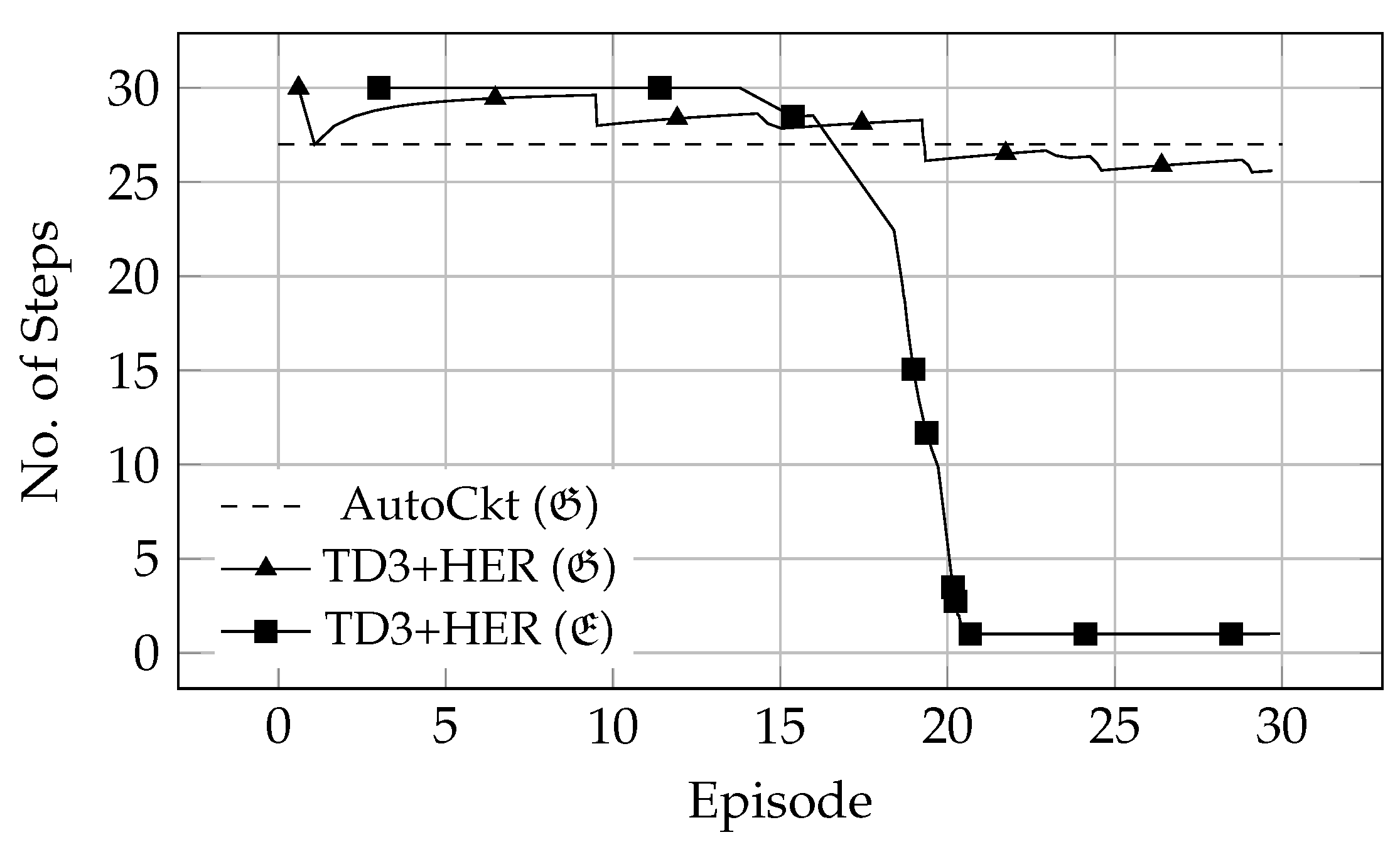
6. Experimental Results

For the evaluation of the proposed method, the three operational amplifiers, shown in Figure A1, were selected primarily to showcase the robustness regarding this class of circuits. All agents were trained in the same nine-dimensional goal space G , defined in Section 5. During the initial training, the agents only get to interact with the environment via transformation models ρ for a real-world 350 n m PDK. On the left in Figure 5, the success rate of each agent is shown, where 100% corresponds to the agent reaching the desired g with t < T steps, averaged over P = 32 parallel environments. The success rates for training in the G domain are omitted in this plot, since the agents fail to achieve any specification over the course of M = 50 episodes, suggesting that a longer training time and reward shaping might be necessary in this domain.
Section 5 introduces efficient design space navigation as the main focus for this approach. Instead of judging the circuit performance with an FOM [34,36,39], the number of simulations t, such that h g ( s t ) = 1 , is the defining metric used to assess the agents’ performance. The number of steps, averaged over P = 32 parallel environments, are plotted versus the training episode on the right side of Figure 5. In addition to the average number of steps t ¯ and success rate after M = 50 episodes, Table 3 also shows the average number of steps it takes an agent to reach the first success and the average number of steps before the agent achieves success with t < 5 steps. By observing Table 4, the benefits of choosing a continuous action space become evident. Upon each environment reset, the agent is confronted with a broken state of the circuit, where some performance metrics cannot even be extracted, which are denoted as N/A in the table. Regardless of how broken this random initial state is or how far it is from the desired goal, the agent proposes a suitable solution almost immediately. This would not be possible in a discrete action space, where the agent is impaired by the step size, such that the efficiency of navigation depends highly on the starting point. Furthermore, Table 4 indicates that, regardless of initial state s 0 and goal g , no explicit expert guidance or reward shaping is necessary. Since the agent is not trained to maximize any FOM, there is never the need for expert intervention or reward shaping [36]; instead, the agent simply navigates to a coordinate in S where h g ( s t ) = 1 such that t T , regardless of whether some performances are already met or not. These observations and results satisfy the goal, defined in Section 5, of this approach. After training for M = 50 episodes, the agents prove to be very capable of design space navigation based on the transformed action space in the E domain. Whether this approach can be successfully applied to other circuit classes remains to be examined in future research. However, if the action and observation spaces are equally well defined with similar dimensions, comparable results are to be expected.

Technology Migration

Table 3 shows, in addition to the previously discussed metrics, the findings regarding the success rate and average number of steps of agents evaluated with transformation models of a different technology without re-training. For this experiment, agents trained in a 350 n m technology were employed on the same circuit, but with different transformation models ρ for a 180 n m technology. As expected, the results confirm the findings presented in Section 4, where procedures written for one technology can be seamlessly re-used simply by swapping the transformation models. Essentially, the agents are oblivious to the technology; they merely propose operating points that yield a certain performance. Regardless of the technology, if all devices are at the same operating point, the overall performance should be comparable as well. By shifting the blame to the transformation models, there is no need for transfer learning [36] to address technology migration. Similar to human experts, the agents have acquired an intuition regarding the electrical behavior of building blocks and their influence on the entire circuit performance. It is important to note when considering different technologies that boundary conditions, such as the supply voltage, can change and some circuit topologies might not be able to achieve the exact same performance specifications. Therefore, these experiments were conducted with identical boundary conditions.
For further illustration, the other example in Table 4 shows how an agent manages to find the same specification in the same amount of steps t, but in a different technology. By never exposing the agents to technology-dependent parameters, they become significantly more versatile.

7. Conclusions

Findings regarding both the knowledge-based and learning-based analog IC sizing methods are discussed and compared to related work in the following sections.

7.1. Knowledge-Based Circuit Sizing

The state-of-the-art, manual g m / I d method for sizing analog ICs based on LUTs was used as the foundation for procedural sizing automation. NNs were trained with the LUT data, effectively modeling the behavior of primitive devices around the operating point, given desired electrical characteristics. Using these models, a sizing procedure for an operational amplifier was expressed in terms of electrical characteristics ( g m / I d f ug ) of building blocks [13] in the circuit.
When employing this method, the primary consideration is the generation of training data and the training of the ML models. With an NVIDIA® RTX  3090, training for one such model took approximately 35 min . The data-generating process had to be performed twice per technology, once for NMOS and PMOS. As soon as the models are available, they can be used in conjunction with an already existing procedure, initially composed of different models, seamlessly porting the sizing strategy to another technology. The effort required in training the first models and programmatically expressing sizing strategies is far outweighed by the resulting re-usability. Furthermore, the sizing strategies of experienced circuit designers are captured in a technology-independent way, which is valuable for both academia and industry.

7.2. Learning-Based Circuit Sizing

The findings of the procedural approach were the basis for the following learning-based approach. If an expert circuit designer can use the g m / I d method to express an iterative sizing strategy in the electrical domain, it stands to reason that an artificial designer can be trained to learn a similar policy. We formulated the sizing task as a sequential decision-making problem, which allowed the use of RL to find a near-optimal solution given weak supervision in the form of a reward signal. Prior work regarding RL for analog IC sizing exists; however, it does not consider an action space in the electrical domain, nor does it focus on efficient design space navigation, which makes a direct comparison difficult.
Unlike related work [34,36,39], our approach trained RL agents with an action space in the electrical domain and a sparse binary reward signal indicating whether the agent had reached the required specifications. We employed HER to increase sample efficiency without relaxing the original problem, which would introduce bias to the optimization procedure. During training, the agent was rewarded for reaching arbitrary states, i.e., sets of specifications after a series of actions. This reward schedule deprecated the need for a hand-crafted FOM, which would otherwise supplement a sparse reward signal in the initial training stages when the agent is unlikely to reach optimal sets of specifications. Subsequently, the agent learned to navigate the state space, allowing it to reach any desired state with ease once training had concluded.
Wang et al. reported training for up to 10 4 simulation steps, while our approach considered 50 × 30 × 32 = 4.8 × 10 4 samples initially. Table 3 shows that the first successes were achieved after 1 3 { 333.91 , 203.50 , 338.22 } × 32 = 9340.05 , simulation steps on average across all three environments, which is just before the 10th episode. Additionally, we observed that, shortly after this, the agents were able to solve the environment in less than five simulation steps. According to Figure 5, the number of samples could be decreased to 30 × 30 × 32 = 2.88 × 10 4 without any impact on performance.
Leveraging an electrical action space makes the agents oblivious to the device geometries. As such, the method is inherently technology-independent, and no transfer learning is required, unlike other approaches [34,36]. The electrical domain, in conjunction with HER, improves the design space navigation abilities of the agents presented here, making it 9 × faster than the ones reported by Settaluri et al.
This behavior demands further analysis since, initially, this was considered a sequential decision-making problem. After training, however, the performance resembled that of supervised learning approaches. Instead of step-by-step progress toward a goal, the agent generates a suitable solution within one or two steps. A naively created dataset for supervised learning in such a space would be comparatively large. For example, the simplest circuit considered here, SYM shown in Figure A1a, with 10 input parameters and 10 values each, would result in a dataset with 10 10 points. With the RL algorithm presented here, it seems the 28.8 × 10 4 data points collected after 30 episodes are sufficient to train an efficacious artificial designer.
Wang et al. drew a comparison between a designer with 5 years of experience, for whom it takes 6 h to size an operational amplifier. Although, most likely only a fraction of a human designer’s training is spent on one specific topology, it is still much more than the 4.5   h training time of the artificial designers presented here. Additionally, the execution time of t 3 simulations of a trained agent is at least three orders of magnitude faster than this manual sizing process reported in [36]. Furthermore, because there is no reward shaping, no prior domain knowledge is biasing or influencing the learning behavior of the agents; they re-discover circuit sizing in the E domain by themselves.

7.3. Summary

Overall, using an electrical design and action space proved very effective for human- and particularly artificial circuit designers in terms of both learning behavior and the portability of trained agents between different technology nodes. The procedural approach presented in Section 4 provides an interface for RL to the g m / I d method, such that agents can learn the art of analog circuit sizing without being tied to a specific technology. Agents trained in this alternative action space gain an understanding of the electrical behavior of the building blocks [13] and do not require any re-training or explicit guidance by human domain experts when used with different technologies. Additionally, the results show that the learned policies were optimized in terms of efficient design space navigation.

Author Contributions

Conceptualization, Y.U., M.B., L.B., J.S. and C.C.; data curation, Y.U.; funding acquisition, J.S. and C.C.; investigation, L.B.; methodology, Y.U.; project administration, J.S. and C.C.; Resources, M.B. and L.B.; Software, Y.U., M.B. and L.B.; supervision, J.S. and C.C.; validation, M.B.; writing—original draft, Y.U.; writing—review and editing, M.B., L.B., J.S. and C.C. All authors have read and agreed to the published version of the manuscript.

Funding

This research was funded by the German Federal Ministry of Education and Research (BMBF) within the project PLASMA under Ref. No. 13FH197PX8.

Data Availability Statement

Source code for both, the procedural approach (https://git.io/Jcgkq, accessed 5 January 2023) and the reinforcement learning approach (https://github.com/electronics-and-drives/mlcad22, accessed 5 January 2023) are available on github.

Conflicts of Interest

The authors declare no conflict of interest.

Abbreviations

The following abbreviations are used in this manuscript:
ACiDartificial circuit designer
BMBFGerman Federal Ministry of Education and Research
BOBayesian optimization
CANcircuit attention network
CNNconvolutional neural network
DDPGdeep deterministic policy gradient
DLdeep learning
DRLdeep reinforcement learning
EDAelectronic design automation
ESevolutionary strategy
FOMfigure of merit
GNNgraph neural network
GCNgraph convolutional network
HERhindsight experience replay
ICintegrated circuit
LUTlook-up table
MAEmean absolute error
MDPMarkov decision process
MLmachine learning
MLPmultilayer perceptron
MSEmean-squared error
NNneural network
PDKprocess design kit
PPOproximal policy optimization
ReLUrectified linear unit
RLreinforcement learning
TD3twin delayed deep deterministic policy gradient
A0DC loop gain
Aeestimated area
CMRRcommon mode rejection ratio
GMgain margin
IDDcurrent consumption
PMphase margin
PSRRpower supply rejection ratio
SRslew rate
UGBWunity gain bandwidth
Voff(1σ)statistical offset
SYMsymmetrical amplifier
MILMiller operational amplifier
FCAfolded cascode amplifier

Appendix A. Circuits

Figure A1. Set of operational amplifiers, where the bulk potentials of NMOS and PMOS are connected to VSS and VDD, respectively.
Electronics 12 00302 g0a1aElectronics 12 00302 g0a1b
These operational amplifiers were used for demonstrating both sizing approaches presented in this work.

Appendix B. Hyperparameters

For the NNs approximating the electrical behavior of primitive devices, the following hyperparameters were used. No optimization or search has been conducted at this time, and further improvements can be expected by tuning these accordingly.
Table A1. Hyperparameters for LUT mapping NNs.
ParameterValue
OptimizerAdam [52]
Learning Rate 1 · 10 3
Number of Hidden Layers7
Number of Hidden Units per Layer [ 128 , 256 , 512 , 1024 , 512 , 256 , 128 , 256 ]
Non-Linearity of Hidden LayersReLU [51]
Batch Size128
Number of Epochs24
The hyperparameters for the TD3 + HER RL agents were taken from the literature [40,41]. Similarly, tuning these might lead to significant improvements.
Table A2. Hyperparameters for TD3 + HER agents.
ParameterValue
OptimizerAdam [52]
Actor Learning Rate 1 · 10 3
Critic Learning Rate 1 · 10 3
Discount Factor ( γ ) 0.99
Number of Hidden Layers2
Number of Hidden Units per Layer256
Non-Linearity of Hidden LayersReLU [51]
Number of Update Steps (E)40
Target Update Interval (d)2
Random Exploration Interval10
Test Interval5
Parallel Environments (P)32
Target Smoothing Coefficient ( τ ) 0.005
Noise Clipping (c) 0.2
Exploration Policy N ( 0 , 0.1 )
Number of Steps per Episode30
Buffer Size 10 6
Batch Size128
Goal Sampling Strategy ( S )future [41]
Number of Additional Goals (k)4

Appendix C. Reinforcement Learning Algorithm

The algorithm is a combination of TD3 [40] and HER [41], as listed in Algorithm A1 below.
Algorithm A1 Artificial circuit designer (ACiD)
  • Initialize critic networks Q θ 1 , Q θ 2 and policy network π ϕ with random parameters θ 1 , θ 2 , and ϕ .
  • Initialize target networks θ 1 θ 1 , θ 2 θ 2 , and ϕ ϕ .
  • Initialize empty replay buffer R .
  • for episode { 0 , , M } do                 ▹ For P parallel environments
  •  Initialize empty episode buffer R e
  •  Get initial state s 0 and goal specification g.
  • for  t { 0 , , T }  do
  •   Concatenate current state and goal o t s t g .
  •   Sample exploration noise ϵ N ( 0 , σ ) .
  •   Sample action with exploration noise a t π ϕ ( o t ) + ϵ .
  •   Convert action to sizing a ¯ t ρ ( a t )
  •   Simulate netlist with sizing a ¯ t , and observe s t + 1 .
  •   Store transition tuple ( s t , a t , r t , d t , s t + 1 ) in R e .
  • end for
  • for  t { 0 , , T }  do
  •   Concatenate state and goal o t s t g , o t + 1 s t + 1 g .
  •   Store transition tuple ( o t , a t , r t , o t + 1 ) in R .
  •   Sample k additional specifications G : = S ( R e ) .
  •   for  g G  do
  •      Calculate reward r g : = r ( s t , a t , g ) .
  •      Concatenate o t s t g , o t + 1 s t + 1 g .
  •      Store transition tuple ( o t , a t , r t , o t + 1 ) in R .
  •   end for
  • end for
  • for  iter { 0 , , E }  do
  •   Sample minibatch of transitions B R .
  •   Sample evaluation noise ϵ ˜ clip ( N ( 0 , σ ˜ ) , c , c )
  •   Predict action a ˜ t + 1 π ϕ ( o t + 1 ) + ϵ ˜ .
  •   Calculate return y r t + γ · min i = [ 1 , 2 ] Q θ i ( o t + 1 , a ˜ t + 1 ) .
  •   Update critics θ i arg min θ i N 1 ( y Q θ i ( o t , a t ) ) 2
  •   if  iter mod d 0  then
  •      Predict action a t π ϕ ( o t ) .
  •      Update ϕ J ( ϕ ) = N 1 a Q θ 1 ( o t , a t ) ϕ π ϕ ( o t ) .
  •   end if
  • end for
  •  Update target critics θ i τ θ i + ( 1 τ ) θ i
  •  Update target policy ϕ τ ϕ + ( 1 τ ) ϕ
  • end for

References

  1. Degrauwe, M.G.R.; Nys, O.; Dijkstra, E.; Rijmenants, J.; Bitz, S.; Goffart, B.L.A.G.; Vittoz, E.A.; Cserveny, S.; Meixenberger, C.; van der Stappen, G.; et al. IDAC: An interactive design tool for analog CMOS circuits. IEEE J. Solid-State Circuits 1987, 22, 1106–1116. [Google Scholar] [CrossRef]
  2. Nye, W.; Riley, D.C.; Sangiovanni-Vincentelli, A.; Tits, A.L. DELIGHT.SPICE: An optimization-based system for the design of integrated circuits. IEEE Trans. Comput.-Aided Des. Integr. Circuits Syst. 1988, 7, 501–519. [Google Scholar] [CrossRef]
  3. Antreich, K.; Koblitz, R. Design centering by yield prediction. IEEE Trans. Circuits Syst. 1982, 29, 88–96. [Google Scholar] [CrossRef]
  4. Scheible, J.; Lienig, J. Automation of Analog IC Layout: Challenges and Solutions. In Proceedings of the 2015 Symposium on International Symposium on Physical Design, ISPD ’15; Association for Computing Machinery: New York, NY, USA, 2015; pp. 33–40. [Google Scholar] [CrossRef] [Green Version]
  5. Lyu, W.; Xue, P.; Yang, F.; Yan, C.; Hong, Z.; Zeng, X.; Zhou, D. An Efficient Bayesian Optimization Approach for Automated Optimization of Analog Circuits. IEEE Trans. Circuits Syst. I Regul. Pap. 2018, 65, 1954–1967. [Google Scholar] [CrossRef]
  6. Castejon, F.; Carmona, E.J. Introducing Modularity and Homology in Grammatical Evolution to Address the Analog Electronic Circuit Design Problem. IEEE Access 2020, 8, 137275–137292. [Google Scholar] [CrossRef]
  7. Scheible, J. Optimized is Not Always Optimal. In Proceedings of the 2022 Symposium on International Symposium on Physical Design, ISPD ’22; Association for Computing Machinery: New York, NY, USA, 2022; pp. 151–158. [Google Scholar] [CrossRef]
  8. Schweikardt, M.; Scheible, J. Expert Design Plan: A Toolbox for Procedural Analog Integrated Circuit Design. In Proceedings of the SMACD/PRIME 2022, International Conference on SMACD and 17th Conference on PRIME, Villasimius, Italy, 12–15 June 2022; pp. 1–4. [Google Scholar]
  9. Jespers, P.G.A.; Murmann, B. Systematic Design of Analog CMOS Circuits: Using Pre-Computed Lookup Tables; Cambridge University Press: Cambridge, UK, 2017. [Google Scholar] [CrossRef]
  10. Silveira, F.; Flandre, D.; Jespers, P.G.A. A gm/ID based methodology for the design of CMOS analog circuits and its application to the synthesis of a silicon-on-insulator micropower OTA. IEEE J. Solid-State Circuits 1996, 31, 1314–1319. [Google Scholar] [CrossRef]
  11. Ochotta, E.S.; Rutenbar, R.A.; Carley, L.R. Synthesis of high-performance analog circuits in ASTRX/OBLX. IEEE Trans. Comput.-Aided Des. Integr. Circuits Syst. 1996, 15, 273–294. [Google Scholar] [CrossRef]
  12. Marolt, D.; Scheible, G.J. A practical layout module pcell concept for analog IC design. In Proceedings of the CDNLive EMEA 2013, Munich, Germany, 12–13 March 2013. [Google Scholar]
  13. Graeb, H.; Zizala, S.; Eckmueller, J.; Antreich, K. The sizing rules method for analog integrated circuit design. In Proceedings of the IEEE/ACM International Conference on Computer Aided Design, ICCAD 2001, IEEE/ACM Digest of Technical Papers (Cat. No.01CH37281), San Jose, CA, USA, 4–8 November 2001; pp. 343–349. [Google Scholar]
  14. Massier, T.; Graeb, H.; Schlichtmann, U. The Sizing Rules Method for CMOS and Bipolar Analog Integrated Circuit Synthesis. IEEE Trans. Comput.-Aided Des. Integr. Circuits Syst. 2008, 27, 2209–2222. [Google Scholar] [CrossRef]
  15. Schweikardt, M.; Uhlmann, Y.; Leber, F.; Scheible, J.; Habal, H. A Generic Procedural Generator for Sizing of Analog Integrated Circuits. In Proceedings of the 2019 15th Conference on Ph.D Research in Microelectronics and Electronics (PRIME), Lausanne, Switzerland, 15–18 July 2019; pp. 17–20. [Google Scholar]
  16. Zhao, Z.; Zhang, L. Deep Reinforcement Learning for Analog Circuit Sizing. In Proceedings of the 2020 IEEE International Symposium on Circuits and Systems (ISCAS), Seville, Spain, 12–14 October 2020; pp. 1–5. [Google Scholar] [CrossRef]
  17. Mina, R.; Jabbour, C.; Sakr, G.E. A Review of Machine Learning Techniques in Analog Integrated Circuit Design Automation. Electronics 2022, 11, 435. [Google Scholar] [CrossRef]
  18. Abiodun, O.I.; Jantan, A.; Omolara, A.E.; Dada, K.V.; Mohamed, N.A.; Arshad, H. State-of-the-art in artificial neural network applications: A survey. Heliyon 2018, 4, e00938. [Google Scholar] [CrossRef] [Green Version]
  19. Ren, S.; He, K.; Girshick, R.; Sun, J. Faster R-CNN: Towards Real-Time Object Detection with Region Proposal Networks. In Proceedings of the Advances in Neural Information Processing Systems; Curran Associates, Inc.: Red Hook, NY, USA, 2015; Volume 28. [Google Scholar]
  20. Chen, L.C.; Papandreou, G.; Schroff, F.; Adam, H. Rethinking Atrous Convolution for Semantic Image Segmentation. Technical Report, 2017, [1706.05587]. Available online: http://xxx.lanl.gov/abs/1706.05587 (accessed on 22 December 2022).
  21. Xiao, B.; Wu, H.; Wei, Y. Simple Baselines for Human Pose Estimation and Tracking. Technical report, 2018, [1804.06208]. Available online: http://xxx.lanl.gov/abs/1804.06208 (accessed on 22 December 2022).
  22. Habal, H.; Tsonev, D.; Schweikardt, M. Compact Models for Initial MOSFET Sizing Based on Higher-order Artificial Neural Networks. In Proceedings of the 2020 ACM/IEEE 2nd Workshop on Machine Learning for CAD (MLCAD), Reykjavik, Iceland, 16–20 November 2020; pp. 111–116. [Google Scholar] [CrossRef]
  23. Xu, J.; Root, D.E. Artificial neural networks for compound semiconductor device modeling and characterization. In Proceedings of the 2017 IEEE Compound Semiconductor Integrated Circuit Symposium (CSICS), Miami, FL, USA, 22–25 October 2017; pp. 1–4. [Google Scholar]
  24. Xu, J.; Root, D.E. Advances in artificial neural network models of active devices. In Proceedings of the 2015 IEEE MTT-S International Conference on Numerical Electromagnetic and Multiphysics Modeling and Optimization (NEMO), Ottawa, ON, Canada, 11–14 August 2015; pp. 1–3. [Google Scholar]
  25. Baker, M.R.; Patil, R.B. Universal Approximation Theorem for Interval Neural Networks. Reliab. Comput. 1998, 4, 235–239. [Google Scholar] [CrossRef]
  26. Kahraman, N.; Yildirim, T. Technology independent circuit sizing for fundamental analog circuits using artificial neural networks. In Proceedings of the 2008 Ph.D. Research in Microelectronics and Electronics, Istanbul, Turkey, 22 June–25 April 2008. [Google Scholar] [CrossRef]
  27. Mendhurwar, K.; Sundani, H.; Aggarwal, P.; Raut, R.; Devabhaktuni, V. A new approach to sizing analog CMOS building blocks using pre-compiled neural network models. Analog. Integr. Circuits Signal Process. 2012, 70, 265–281. [Google Scholar] [CrossRef]
  28. Islamoglu, G.; Cakici, T.O.; Afacan, E.; Dundar, G. Artificial Neural Network Assisted Analog IC Sizing Tool. In Proceedings of the 2019 16th International Conference on Synthesis, Modeling, Analysis and Simulation Methods and Applications to Circuit Design (SMACD), Lausanne, Switzerland, 15–18 July 2019. [Google Scholar] [CrossRef]
  29. Mnih, V.; Kavukcuoglu, K.; Silver, D.; Graves, A.; Antonoglou, I.; Wierstra, D.; Riedmiller, M. Playing Atari with Deep Reinforcement Learning 2013. [arXiv:cs.LG/1312.5602]. Available online: http://xxx.lanl.gov/abs/1312.5602 (accessed on 22 December 2022).
  30. Silver, D.; Huang, A.; Maddison, C.J.; Guez, A.; Sifre, L.; van den Driessche, G.; Schrittwieser, J.; Antonoglou, I.; Panneershelvam, V.; Lanctot, M.; et al. Mastering the game of Go with deep neural networks and tree search. Nature 2016, 529, 484–489. [Google Scholar] [CrossRef] [PubMed]
  31. Amini, A.; Gilitschenski, I.; Phillips, J.; Moseyko, J.; Banerjee, R.; Karaman, S.; Rus, D. Learning robust control policies for end-to-end autonomous driving from data-driven simulation. IEEE Robot. Autom. Lett. 2020, 5, 1143–1150. [Google Scholar] [CrossRef]
  32. Abbeel, P.; Coates, A.; Quigley, M.; Ng, A. An application of reinforcement learning to aerobatic helicopter flight. Adv. Neural Inf. Process. Syst. 2006, 19, 1–8. [Google Scholar]
  33. Levine, S.; Finn, C.; Darrell, T.; Abbeel, P. End-to-end training of deep visuomotor policies. J. Mach. Learn. Res. 2016, 17, 1334–1373. [Google Scholar]
  34. Settaluri, K.; Haj-Ali, A.; Huang, Q.; Hakhamaneshi, K.; Nikolic, B. AutoCkt: Deep Reinforcement Learning of Analog Circuit Designs, 2020. In Proceedings of the 2020 Design, Automation & Test in Europe Conference & Exhibition (DATE), Grenoble, France, 9–13 March 2020. [Google Scholar] [CrossRef]
  35. Schulman, J.; Wolski, F.; Dhariwal, P.; Radford, A.; Klimov, O. Proximal Policy Optimization Algorithms. arXiv 2017, arXiv:1707.06347. [Google Scholar]
  36. Wang, H.; Wang, K.; Yang, J.; Shen, L.; Sun, N.; Lee, H.S.; Han, S. GCN-RL Circuit Designer: Transferable Transistor Sizing with Graph Neural Networks and Reinforcement Learning, 2020. In Proceedings of the 2020 57th ACM/IEEE Design Automation Conference (DAC), San Francisco, CA, USA, 20–24 July 2020. [Google Scholar] [CrossRef]
  37. Lillicrap, T.P.; Hunt, J.J.; Pritzel, A.; Heess, N.; Erez, T.; Tassa, Y.; Silver, D.; Wierstra, D. Continuous control with deep reinforcement learning. In Proceedings of the 4th International Conference on Learning Representations, ICLR 2016, San Juan, Puerto Rico, 2–4 May 2016; Bengio, Y., LeCun, Y., Eds.; Microtome Publishing: Brookline, MA, USA, 2016. [Google Scholar]
  38. Ng, A.Y.; Harada, D.; Russell, S. Policy invariance under reward transformations: Theory and application to reward shaping. In Proceedings of the International Conference on Machine Learning, Bled, Slovenia, 27–30 June 1999; Volume 99, pp. 278–287. [Google Scholar]
  39. Li, Y.; Lin, Y.; Madhusudan, M.; Sharma, A.; Sapatnekar, S.; Harjani, R.; Hu, J. A Circuit Attention Network-Based Actor-Critic Learning Approach to Robust Analog Transistor Sizing. In Proceedings of the 2021 ACM/IEEE 3rd Workshop on Machine Learning for CAD (MLCAD), Raleigh, NC, USA, 30 August–3 September 2021; pp. 1–6. [Google Scholar] [CrossRef]
  40. Fujimoto, S.; van Hoof, H.; Meger, D. Addressing Function Approximation Error in Actor-Critic Methods. Technical Report. 2018. Available online: http://xxx.lanl.gov/abs/1802.09477 (accessed on 22 December 2022).
  41. Andrychowicz, M.; Wolski, F.; Ray, A.; Schneider, J.; Fong, R.; Welinder, P.; McGrew, B.; Tobin, J.; Pieter Abbeel, O.; Zaremba, W. Hindsight Experience Replay. In Proceedings of the Advances in Neural Information Processing Systems; Curran Associates, Inc.: Red Hook, NY, USA, 2017; Volume 30. [Google Scholar]
  42. Schweikardt, M.; Scheible, J. Improvement of Simulation-Based Analog Circuit Sizing using Design-Space Transformation. In Proceedings of the SMACD/PRIME 2021, International Conference on SMACD and 16th Conference on PRIME, Online, 19–22 July 2021; pp. 1–4. [Google Scholar]
  43. Youssef, A.A.; Murmann, B.; Omran, H. Analog IC Design Using Precomputed Lookup Tables: Challenges and Solutions. IEEE Access 2020, 8, 134640–134652. [Google Scholar] [CrossRef]
  44. Uhlmann, Y.; Essich, M.; Schweikardt, M.; Scheible, J.; Curio, C. Machine Learning Based Procedural Circuit Sizing and DC Operating Point Prediction. In Proceedings of the SMACD/PRIME 2021, International Conference on SMACD and 16th Conference on PRIME, Online, 19–22 July 2021; pp. 1–4. [Google Scholar]
  45. Uhlmann, Y.; Essich, M.; Bramlage, L.; Scheible, J.; Curio, C. Deep Reinforcement Learning for Analog Circuit Sizing with an Electrical Design Space and Sparse Rewards. In Proceedings of the 2022 ACM/IEEE Workshop on Machine Learning for CAD, MLCAD ’22; Association for Computing Machinery: New York, NY, USA, 2022; pp. 21–26. [Google Scholar] [CrossRef]
  46. Liu, W.; Jin, X.; Chen, J.; Jeng, M.C.; Liu, Z.; Cheng, Y.; Chen, K.; Chan, M.; Hui, K.; Huang, J.; et al. BSIM 3v3.2 MOSFET Model Users’ Manual; Technical Report UCB/ERL M98/51; EECS Department, University of California: Berkeley, CA, USA, 1998. [Google Scholar]
  47. Liu, W.; Cao, K.; Jin, X.; Hu, C. BSIM 4.0.0 Technical Notes; Technical Report UCB/ERL M00/39; EECS Department, University of California: Berkeley, CA, USA, 2000. [Google Scholar]
  48. Iskander, R.; Louërat, M.M.; Kaiser, A. Automatic DC operating point computation and design plan generation for analog IPs. In Proceedings of the Analog Integrated Circuits and Signal Processing—Volume 56; Springer US: Boston, MA, USA, 2008; pp. 717–740. [Google Scholar] [CrossRef]
  49. Efraimidis, P.; Spirakis, P. Weighted Random Sampling. In Encyclopedia of Algorithms; Kao, M.Y., Ed.; Springer US: Boston, MA, USA, 2008; pp. 1024–1027. [Google Scholar] [CrossRef]
  50. Box, G.E.P.; Cox, D.R. An analysis of transformations. J. R. Stat. Soc. Ser. (Methodol.) 1964, 211–243. [Google Scholar] [CrossRef]
  51. Glorot, X.; Bordes, A.; Bengio, Y. Deep Sparse Rectifier Neural Networks. In Proceedings of the Fourteenth International Conference on Artificial Intelligence and Statistics; Proceedings of Machine Learning Research. Gordon, G., Dunson, D., Dudík, M., Eds.; PMLR: Fort Lauderdale, FL, USA, 2011; Volume 15, pp. 315–323. [Google Scholar]
  52. Kingma, D.P.; Ba, J. Adam: A Method for Stochastic Optimization; Conference Track Proceedings, 2015. In Proceedings of the 3rd International Conference on Learning Representations, ICLR 2015, San Diego, CA, USA, 7–9 May 2015. [Google Scholar]
  53. Head, T.; Kumar, M.; Nahrstaedt, H.; Louppe, G.; Shcherbatyi, I. Scikit-Optimize. 2021. Available online: https://scikit-optimize.github.io/stable/ (accessed on 22 December 2022).
  54. Reynolds, J.C. Definitional Interpreters for Higher-Order Programming Languages. In Proceedings of the ACM Annual Conference—Volume 2, ACM ’72; Association for Computing Machinery: New York, NY, USA, 1972; pp. 717–740. [Google Scholar] [CrossRef]
  55. Schaul, T.; Horgan, D.; Gregor, K.; Silver, D. Universal Value Function Approximators. In Proceedings of the 32nd International Conference on Machine Learning; Proceedings of Machine Learning Research; Bach, F., Blei, D., Eds.; PMLR: Lille, France, 2015; Volume 37, pp. 1312–1320. [Google Scholar]
  56. Brockman, G.; Cheung, V.; Pettersson, L.; Schneider, J.; Schulman, J.; Tang, J.; Zaremba, W. Openai gym. arXiv 2016, arXiv:1606.01540. [Google Scholar]
  57. Cadence Design Systems, Inc.Spectre Simulation Platform. Technical Report. 2020. Available online: https://www.cadence.com/content/dam/cadence-www/global/en_US/documents/tools/custom-ic-analog-rf-design/spectre-simulation-platform-ds.pdf (accessed on 22 December 2022).
  58. Huang, A.; Hashimoto, J.; Stites, S.; Scholak, T. HaskTorch. 2017. Available online: http://hasktorch.org/ (accessed on 22 December 2022).
  59. Raffin, A.; Hill, A.; Gleave, A.; Kanervisto, A.; Ernestus, M.; Dormann, N. Stable-Baselines3: Reliable Reinforcement Learning Implementations. J. Mach. Learn. Res. 2021, 22, 1–8. [Google Scholar]
  60. Silver, D.; Lever, G.; Heess, N.; Degris, T.; Wierstra, D.; Riedmiller, M. Deterministic Policy Gradient Algorithms. In Proceedings of the 31st International Conference on Machine Learning; Proceedings of Machine Learning Research; Xing, E.P., Jebara, T., Eds.; PMLR: Bejing, China, 2014; Volume 32, pp. 387–395. [Google Scholar]
Figure 1. Histograms of scaled drain current I ^ d [ 0 , 1 ] , showing how the distribution changes for different sampling techniques [44].
Electronics 12 00302 g001
Figure 2. Primitive device (NMOS) models compared to the LUT for length L { 464.16 nm, 1.29 nm, 5.99 nm} [44].
Electronics 12 00302 g002
Figure 3. Comparison between electrical ( E ) and geometrical ( G ) design spaces with Miller operational amplifier as described in [34] as shown by Uhlmann et al. in [45].
Electronics 12 00302 g003
Figure 4. RL framework for analog IC sizing, first shown in [45].
Electronics 12 00302 g004
Figure 5. Average success rate over P = 32 environments [45] during M = 50 training episodes is shown on the left. The right shows the average number of steps it takes an agent to reach g from an arbitrary s 0 .
Electronics 12 00302 g005
Table 1. Specification for procedural sizing examples.
ParameterVDDVin,cmVout,cmIB0CL
Specification3.30 V1.65 V1.65 V3.00 μA10.00 pF
Table 2. Target specification for procedural sizing examples.
ParameterUnitTargetResult
DC loop gain ( A 0 )dB>60.0060.70
unity gain bandwidth (UGBW)MHz> 7.507.80
common mode rejection ratio (CMRR)dB>100.00118.47
power supply rejection ratio (PSRR)dB>80.0080.61
Slew Rate (SR)V/μs>4.004.52
phase margin (PM)°>80.0080.03
statistical offset ( V off ( 1 σ ) )mV<5.004.71
Table 3. All agents are trained with transformation models ρ for a 350 n m technology and evaluated later with models for a 180 n m technology. All step values t ¯ are averaged over P = 32 parallel environments. Shown is the number of steps until the first successful trajectory, the number of steps when an agent first succeeds with less than 5 steps, as well as the success rate and the number of steps to succeed after M = 50 training episodes.
Environment350 nm (Trained)180 nm (Evaluated)
First r = 0 First t ¯ < 5 Success t ¯ Success t ¯
SYM ( E ) 333.91 336.94 100.00% 1.00 82.29% 1.27
MIL ( E ) 203.50 218.41 97.92% 1.10 75.00% 1.00
FCA ( E ) 338.22 392.53 100.00% 1.03 100.00% 1.02
Table 4. Initial and final step of a successful episode, by an agent trained on folded cascode amplifier (FCA) in 350 nm and tested on 180 nm.
ParameterUnitg350 nm180 nm
s0sts0st
A 0 dB≥75.0 27.23 77.32 59.52 76.03
UGBW M Hz ≥2.5N/A 2.51 N/A 2.58
SR V / m s ≥500N/A 515.87 N/A 565.32
PM ≥80.00 85.54 0 82.79
CMRRdB≥120.0 116.69 134.70 43.98 125.24
PSRRdB≥100.0 107.49 127.53 17.18 109.21
V off ( 1 σ ) m V ≤1.5 0.032 1.06 1.39 0.85
I DD μ A ≤25.0 70.87 24.08 202.61 24.30
A e μ m 2≤6.0 10.03 5.83 113.72 4.24
t<300202
Disclaimer/Publisher’s Note: The statements, opinions and data contained in all publications are solely those of the individual author(s) and contributor(s) and not of MDPI and/or the editor(s). MDPI and/or the editor(s) disclaim responsibility for any injury to people or property resulting from any ideas, methods, instructions or products referred to in the content.

