Author Contributions
Conceptualisation, M.B., G.K. and K.P.; methodology, A.B., P.K, M.S. (Mikolaj Sowinski) and W.M.Z.; software, M.K. (Michal Kiecana), P.K., M.K. (Michal Kuc), M.K. (Michal Kuklewski), M.S. (Mikolaj Sowinski) and J.S.; validation, M.B., M.P. and Ł.Ś.; formal analysis, A.B. and M.K. (Michal Kiecana); investigation, A.B., J.G., M.K. (Michal Kiecana) and M.K. (Michal Kuc); resources, A.D., J.G. and M.S. (Maciej Sitek); data curation, M.K. (Michal Kiecana); writing—original draft, M.B., A.B., P.K., M.K. (Michal Kuklewski), M.P. and M.S. (Mikolaj Sowinski); writing—review and editing, M.B., G.K., M.P., Ł.Ś. and J.S.; visualisation, E.J., M.K. (Michal Kiecana) and M.P.; supervision, M.B.; project administration, M.B.; funding acquisition, M.B. and A.S.-K. All authors have read and agreed to the published version of the manuscript.
Figure 1.
Scintillator in an aluminium profile 1744 × 80 × 30 mm.
Figure 1.
Scintillator in an aluminium profile 1744 × 80 × 30 mm.
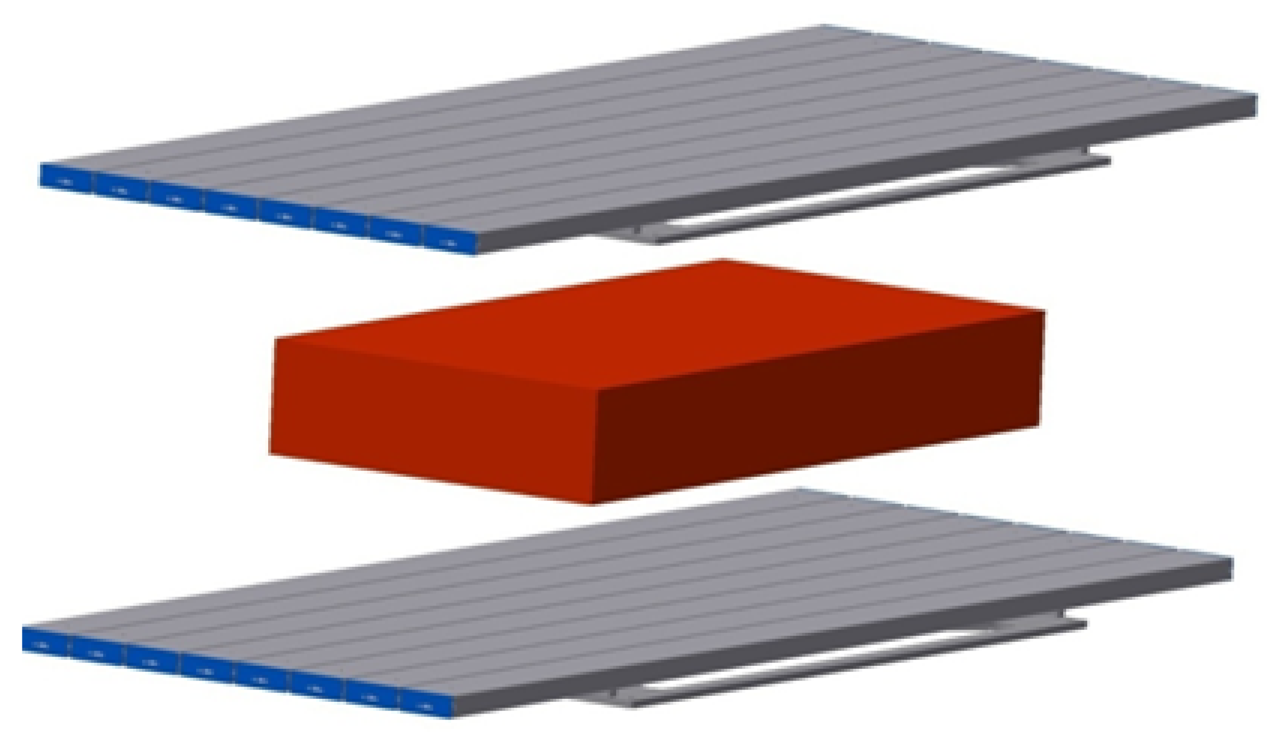
Figure 2.
Two MCORD sections (grey) in coincidence mode. The setup used for testing another detector (red).
Figure 2.
Two MCORD sections (grey) in coincidence mode. The setup used for testing another detector (red).
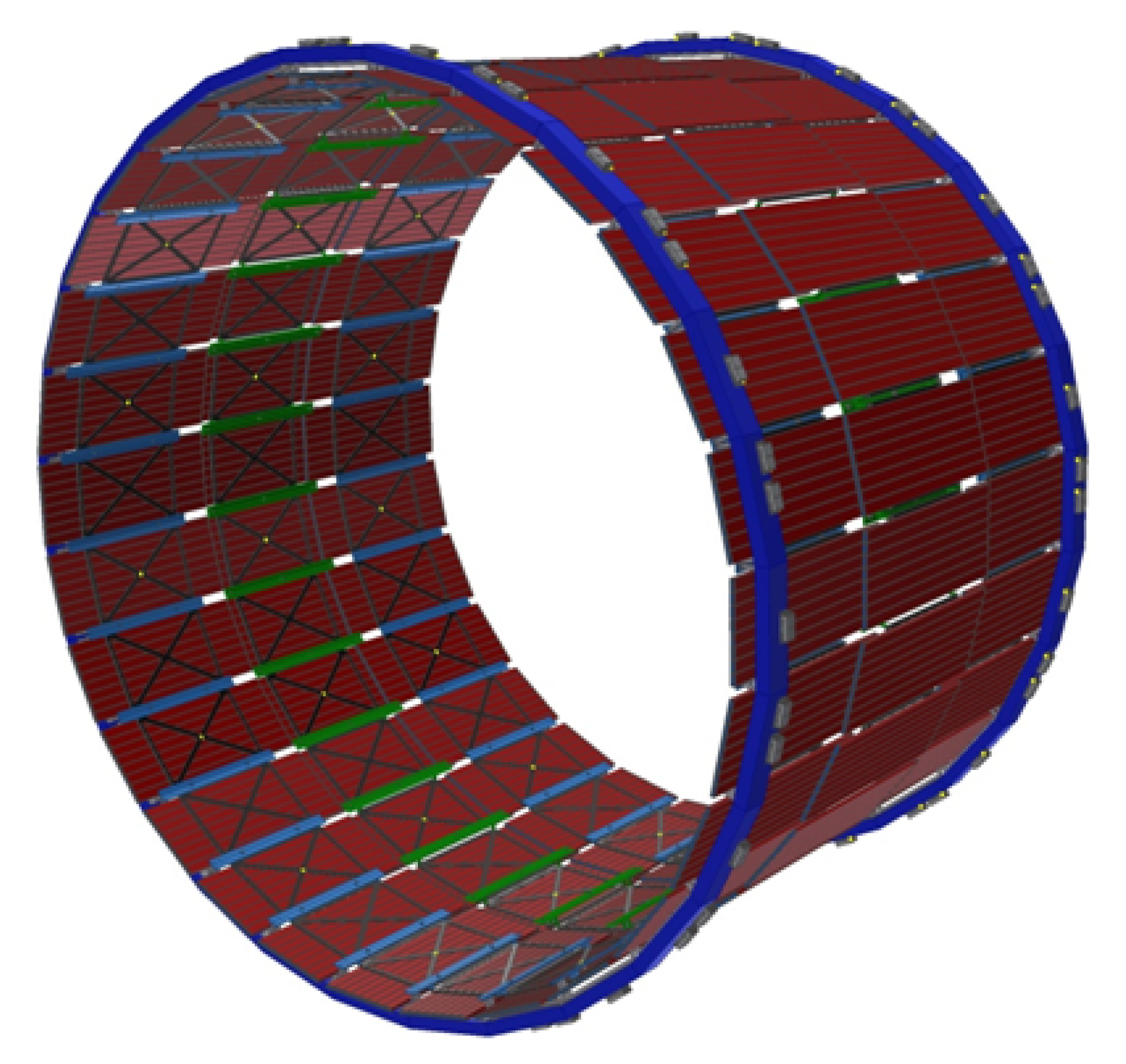
Figure 3.
A cylindrical detector constructed of 84 MCORD sections.
Figure 3.
A cylindrical detector constructed of 84 MCORD sections.
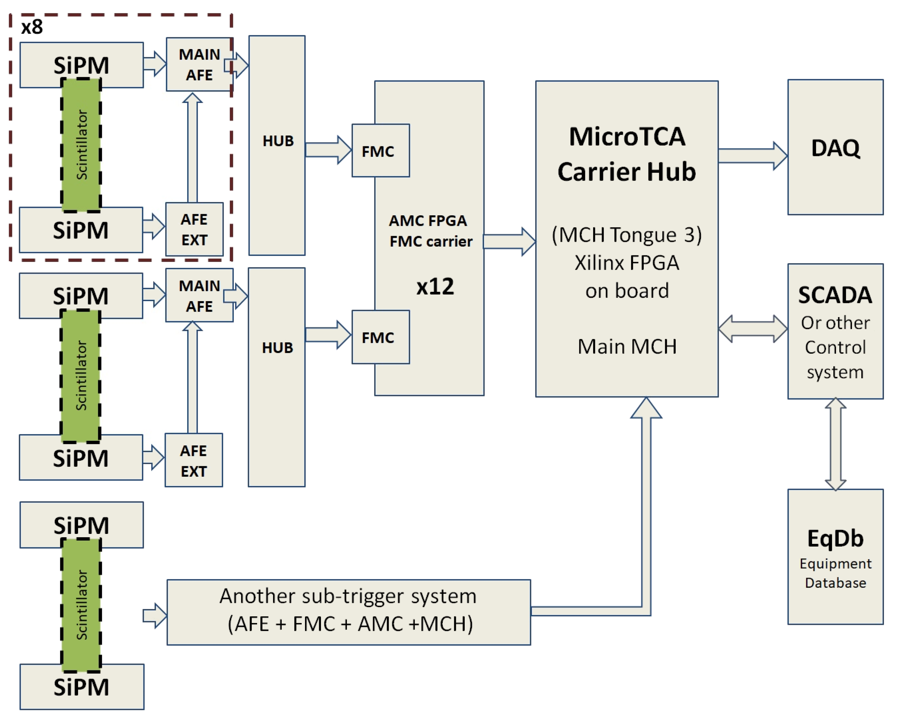
Figure 4.
Block scheme of the whole MCORD electronic system.
Figure 4.
Block scheme of the whole MCORD electronic system.
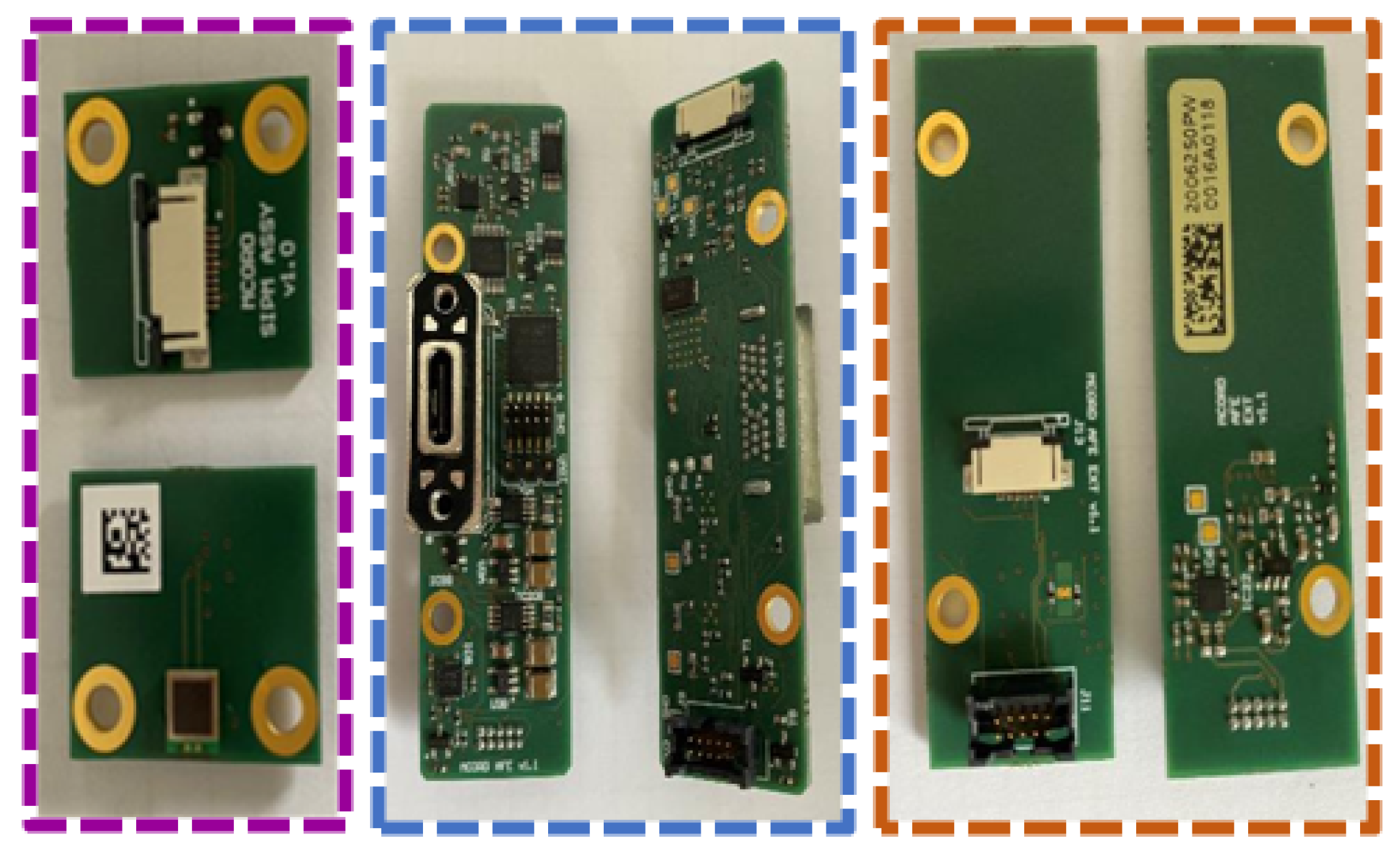
Figure 5.
MCORD AFE electronic boards viewed from both sides. SiPM socket with installed SiPM detector (left, purple), main AFE (centre, blue), and external AFE (right, orange).
Figure 5.
MCORD AFE electronic boards viewed from both sides. SiPM socket with installed SiPM detector (left, purple), main AFE (centre, blue), and external AFE (right, orange).
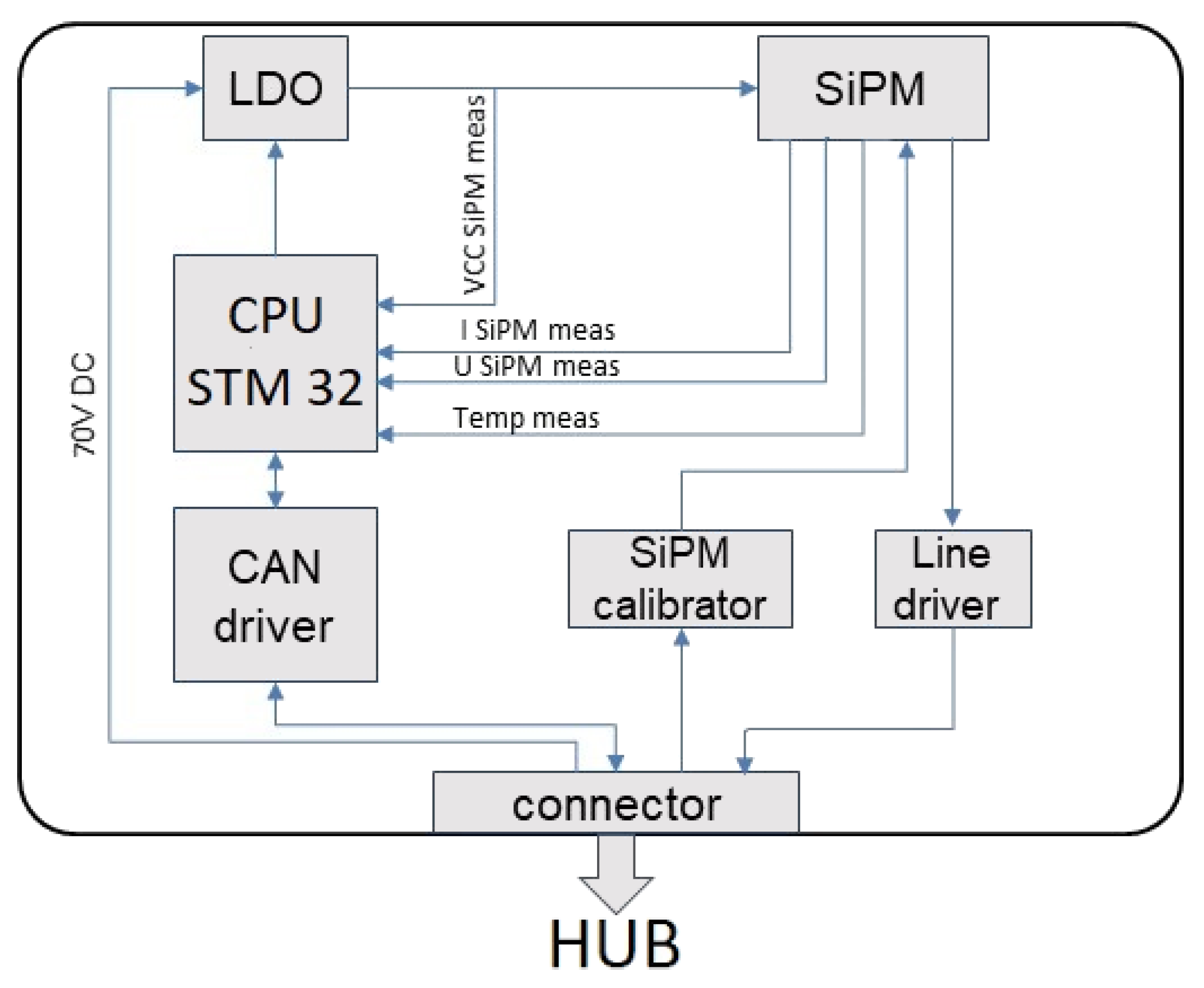
Figure 6.
MCORD AFE layout.
Figure 6.
MCORD AFE layout.
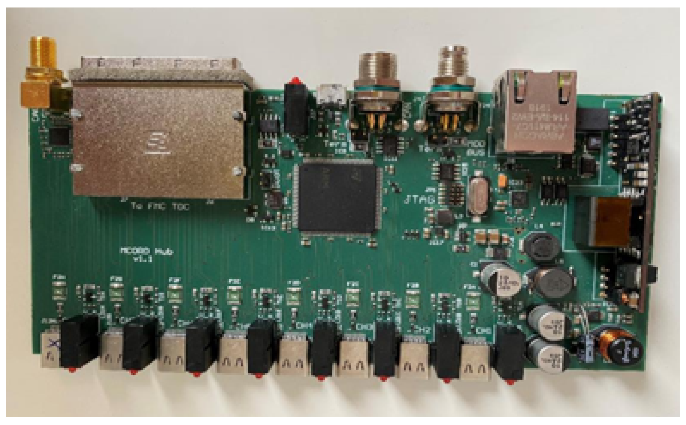
Figure 7.
MCORD HUB electronics board.
Figure 7.
MCORD HUB electronics board.
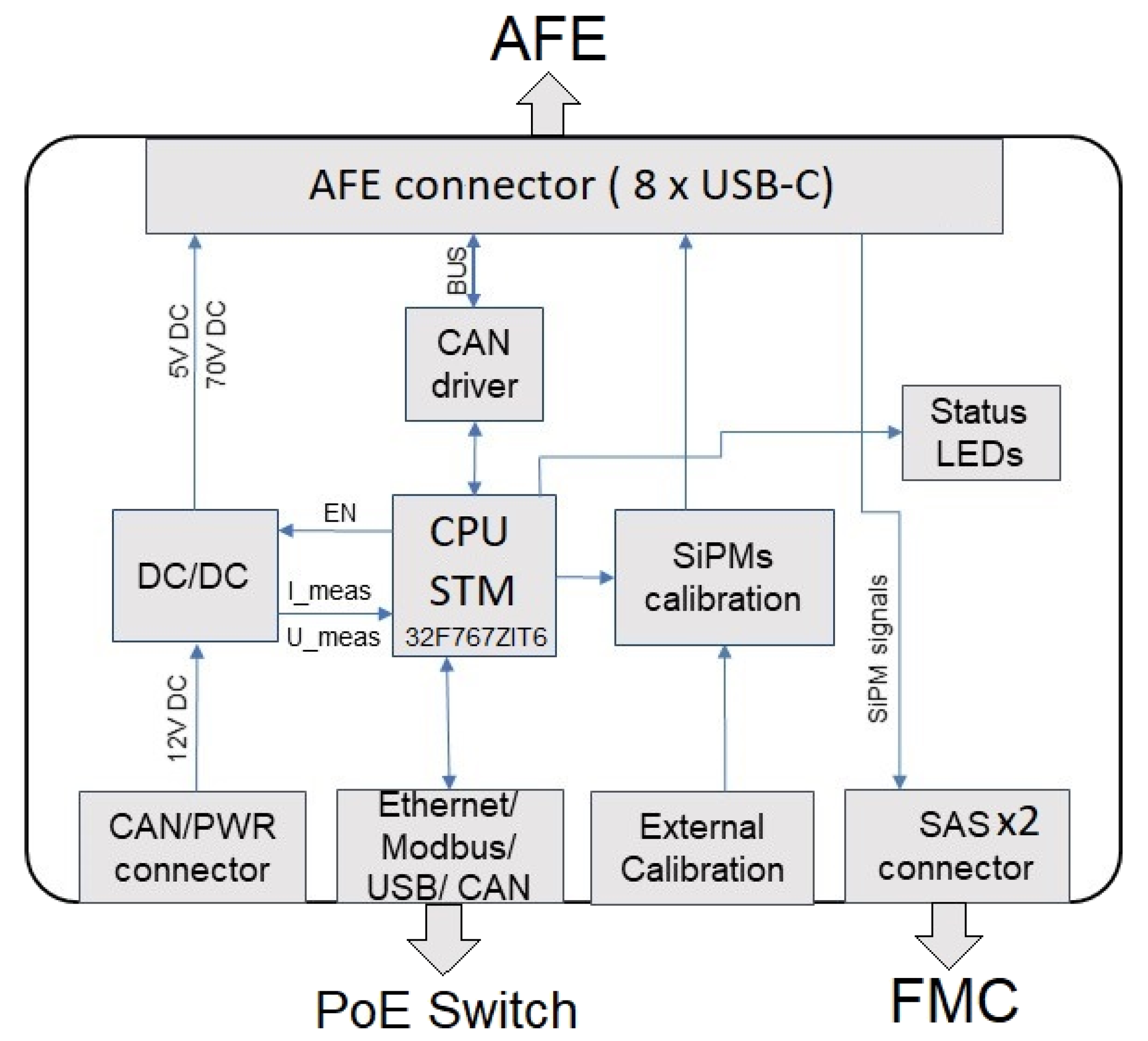
Figure 8.
MCORD HUB idea scheme.
Figure 8.
MCORD HUB idea scheme.
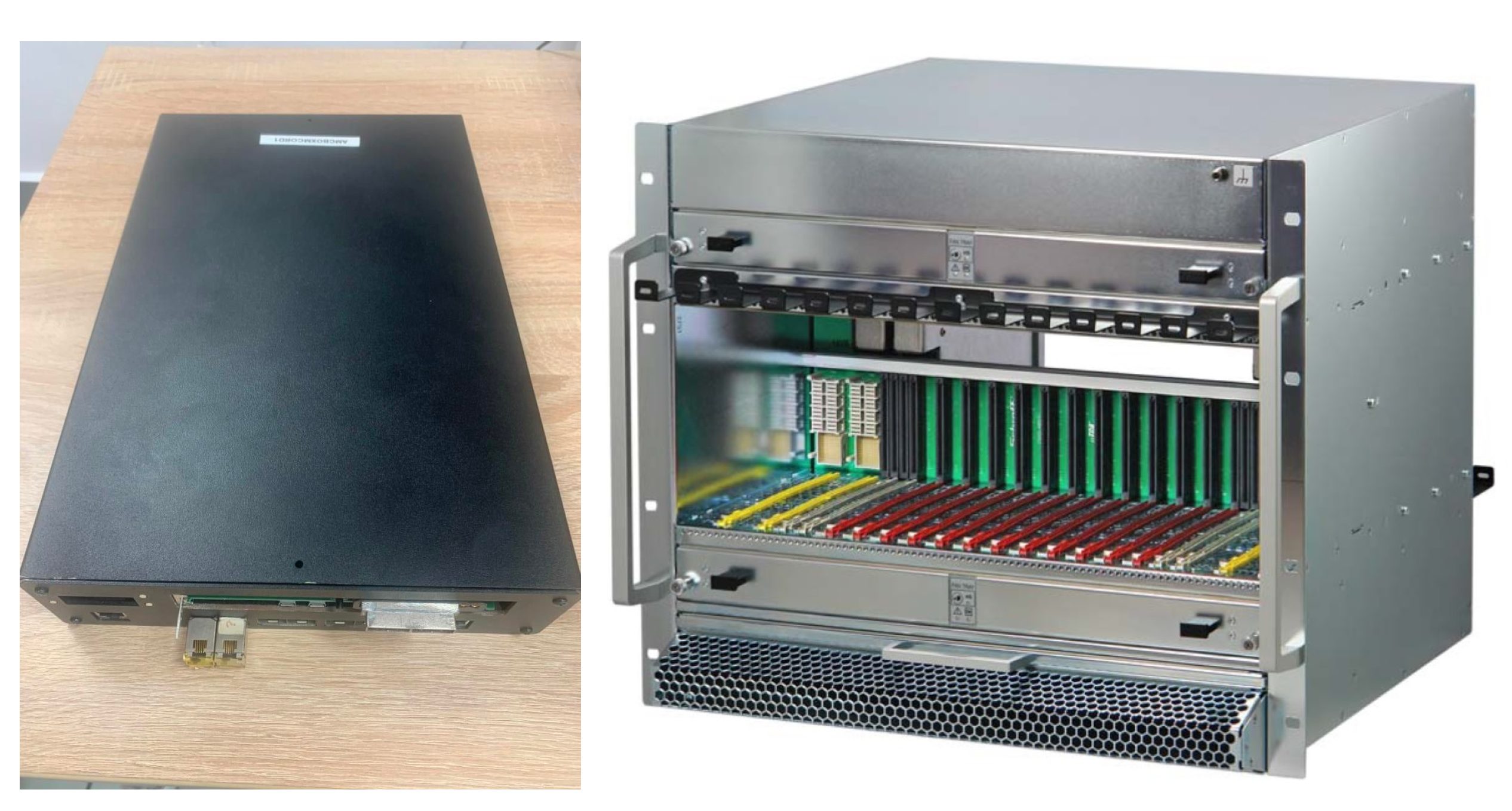
Figure 9.
mTCA chassis for one AMC board (left) and standard mTCA rack for up to 12 AMC (right).
Figure 9.
mTCA chassis for one AMC board (left) and standard mTCA rack for up to 12 AMC (right).
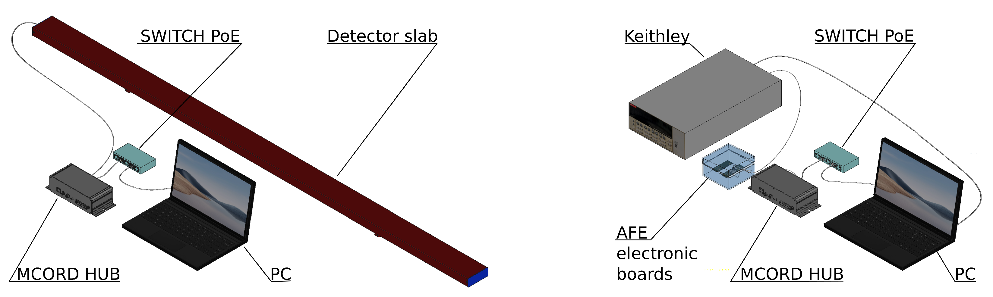
Figure 10.
Visualisation of the measuring station using the complete MCORD detector slab (left), and when the AFE plates are separated from the detector slab to be used with an external precision Keithley meter (right).
Figure 10.
Visualisation of the measuring station using the complete MCORD detector slab (left), and when the AFE plates are separated from the detector slab to be used with an external precision Keithley meter (right).
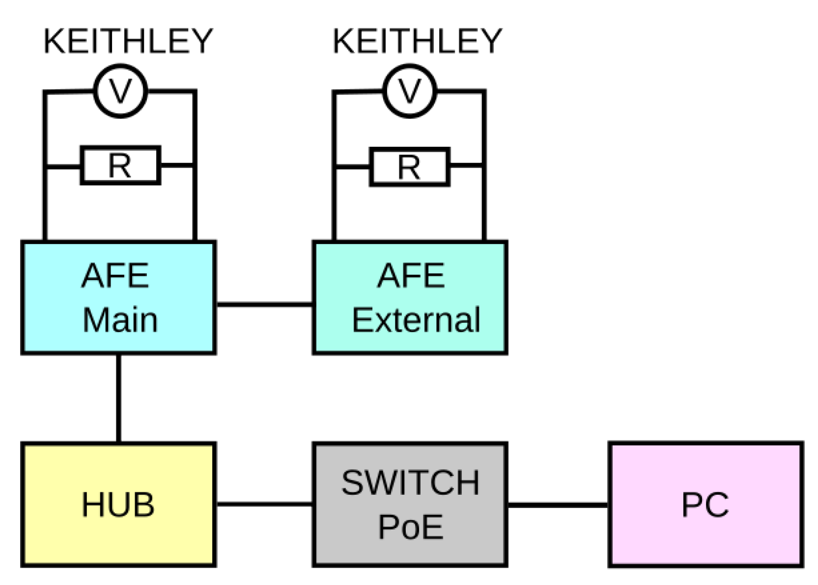
Figure 11.
Schematic diagram of the measuring station for calibration measurements (visualisation shown in
Figure 10, right).
Figure 11.
Schematic diagram of the measuring station for calibration measurements (visualisation shown in
Figure 10, right).
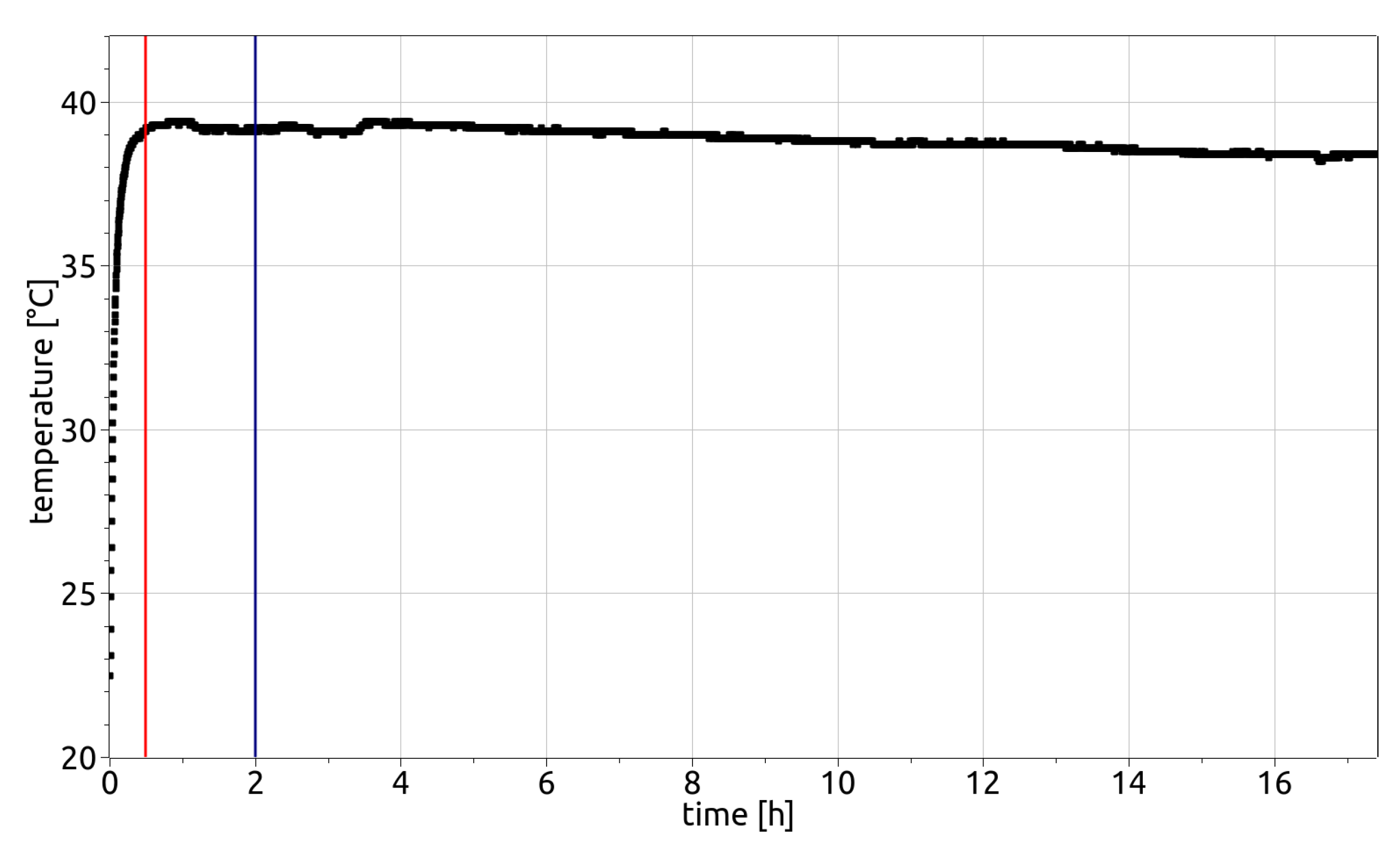
Figure 12.
The heat-up curve of AFE no. 10 measured inside the housing using a thermocouple and Keithley 6517A electrometer.
Figure 12.
The heat-up curve of AFE no. 10 measured inside the housing using a thermocouple and Keithley 6517A electrometer.
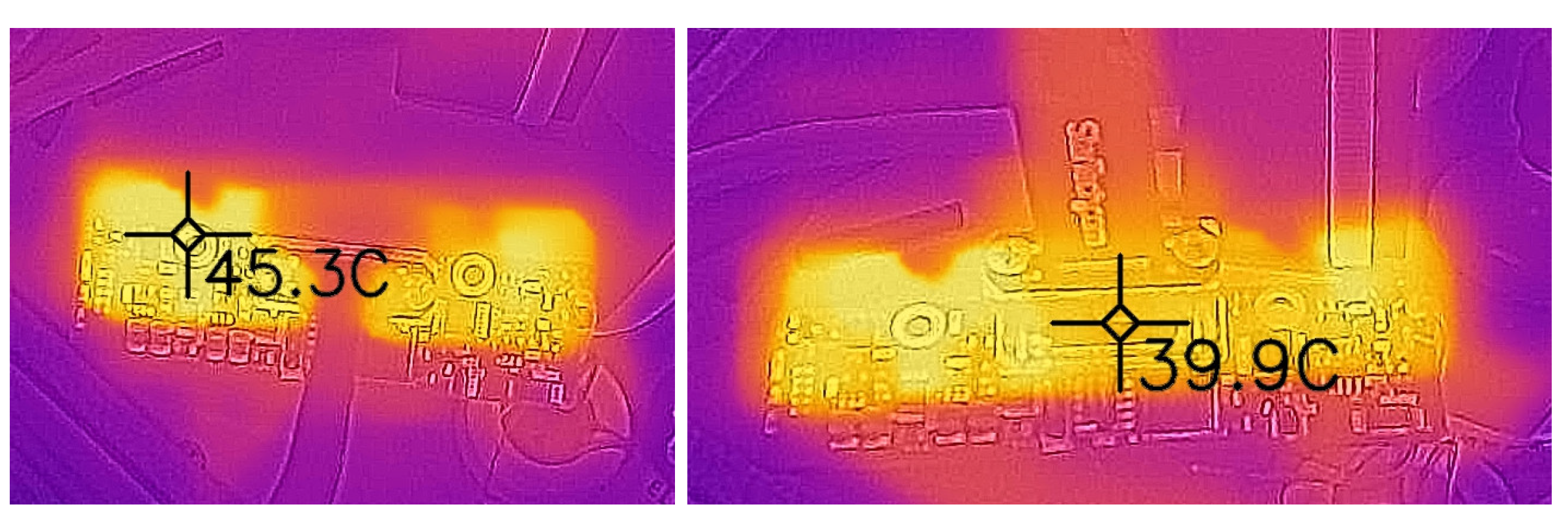
Figure 13.
Photographs of AFE electronics taken with a thermal imaging camera (Flir One by Teledyne) superimposed on regular image (with small misalignment due to parallax). The black crosses show the temperature measurement points. One can see the connected USB-C cable.
Figure 13.
Photographs of AFE electronics taken with a thermal imaging camera (Flir One by Teledyne) superimposed on regular image (with small misalignment due to parallax). The black crosses show the temperature measurement points. One can see the connected USB-C cable.
Figure 14.
Voltage U during heat-up of main AFE measured using the Keithley voltmeter.
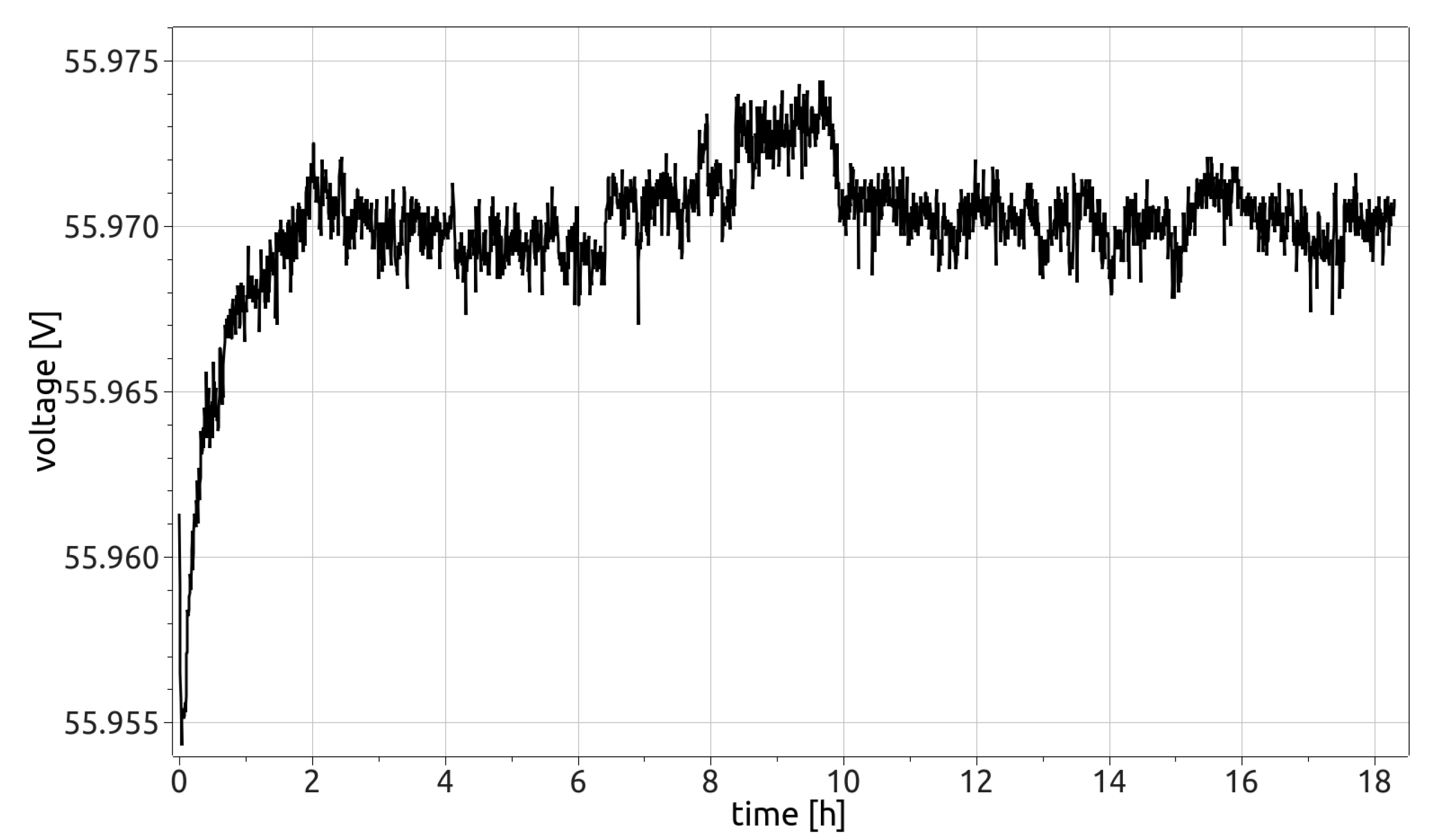
Figure 14.
Voltage U during heat-up of main AFE measured using the Keithley voltmeter.
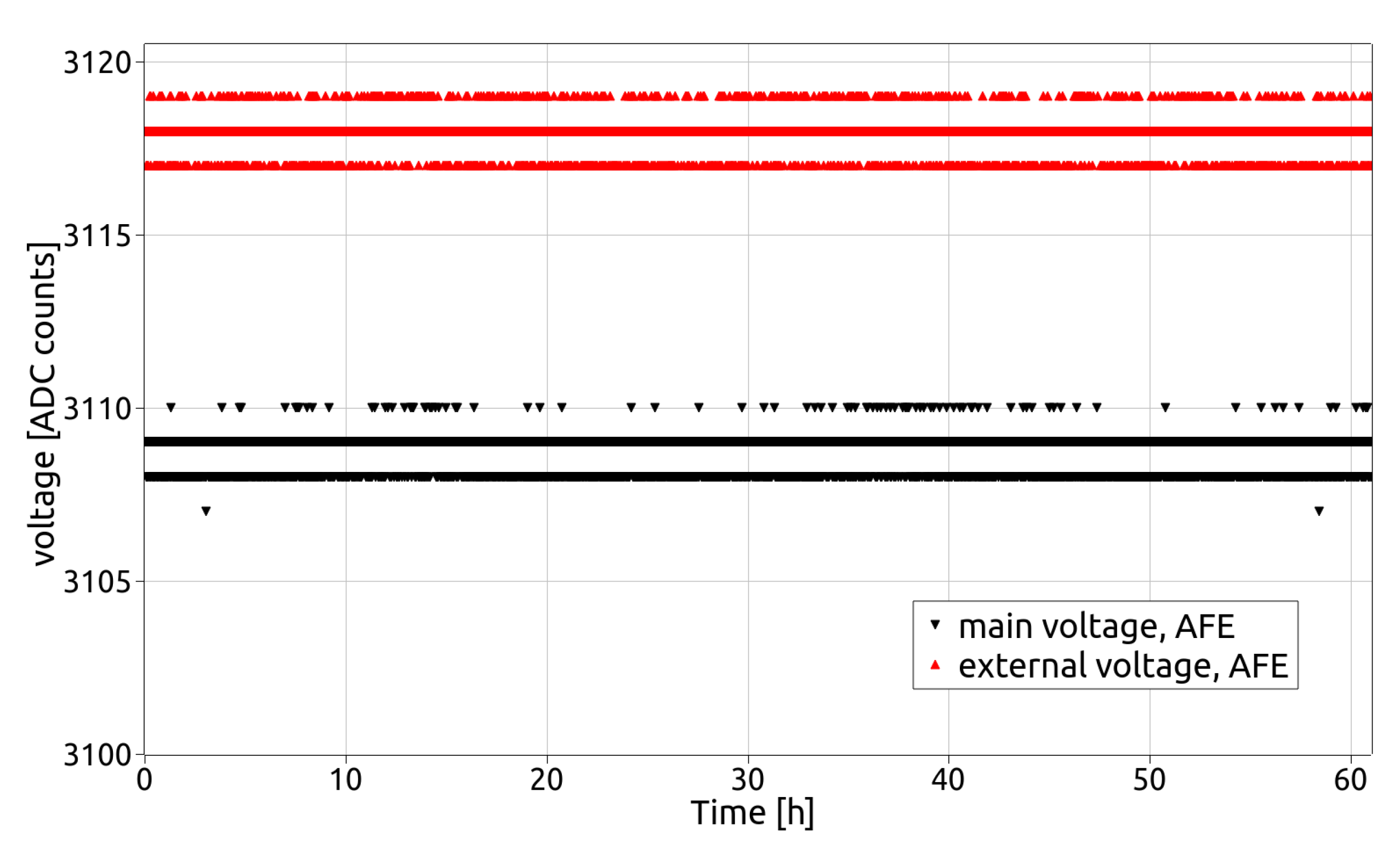
Figure 15.
Long-term voltage stability measured using AFE internal voltmeter. Voltage is given in ADC counts.
Figure 15.
Long-term voltage stability measured using AFE internal voltmeter. Voltage is given in ADC counts.
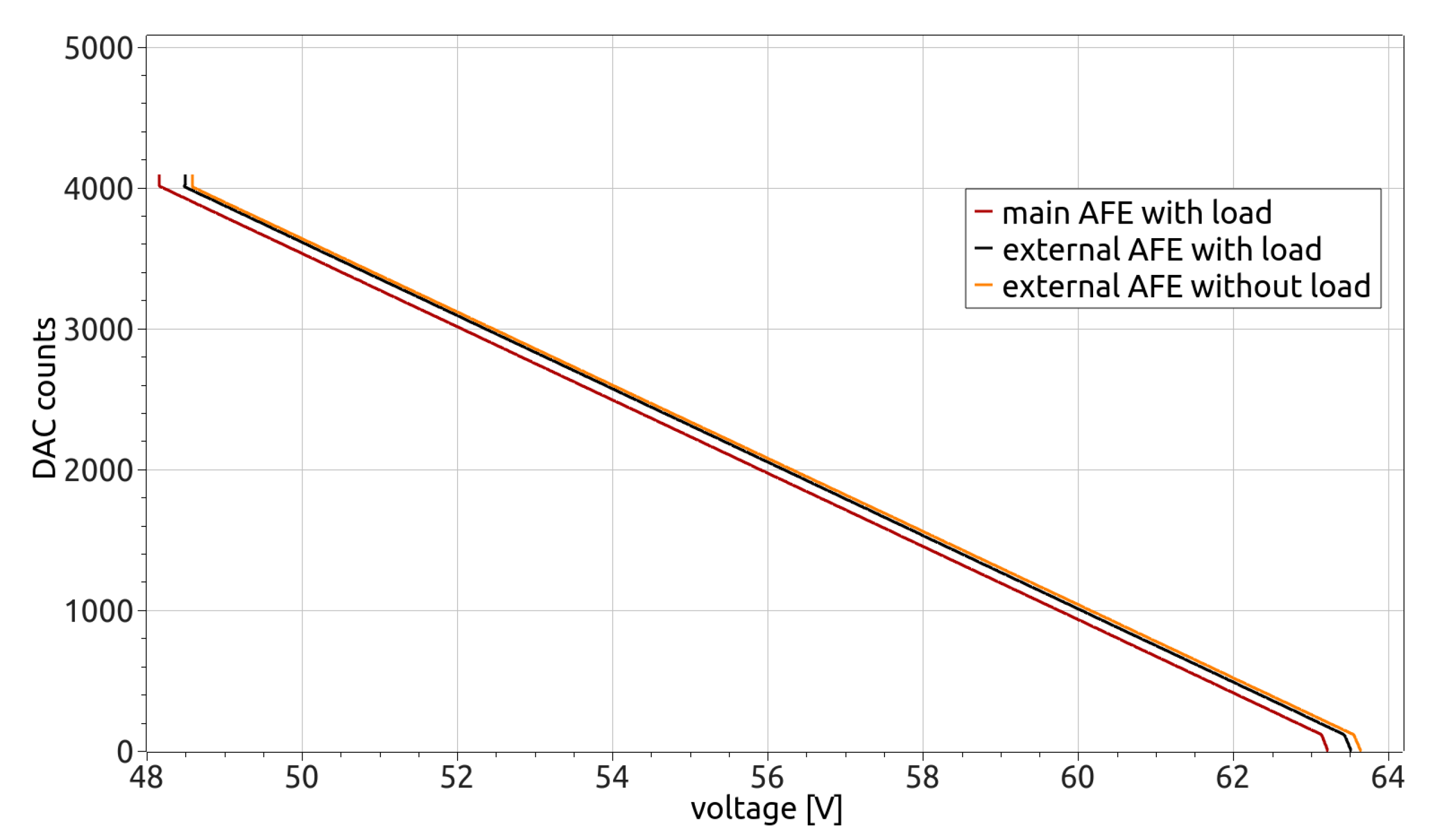
Figure 16.
DAC code that sets supply voltage, x-axis, vs. main and external AFE SiPM voltage (with and without 10.48 M of resistive load), y-axis.
Figure 16.
DAC code that sets supply voltage, x-axis, vs. main and external AFE SiPM voltage (with and without 10.48 M of resistive load), y-axis.
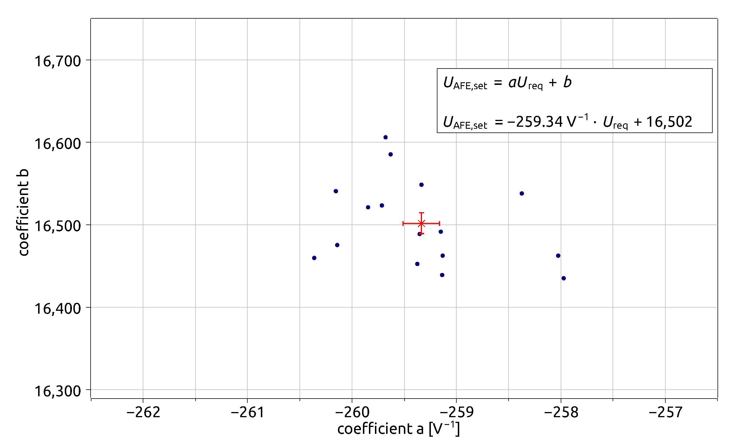
Figure 17.
Distribution calibration coefficients across many AFEs for AFE voltage supply. The scale is limited to a narrow range to show small differences in presented values. The average values are marked with a red marker and given as an example below the formula.
Figure 17.
Distribution calibration coefficients across many AFEs for AFE voltage supply. The scale is limited to a narrow range to show small differences in presented values. The average values are marked with a red marker and given as an example below the formula.
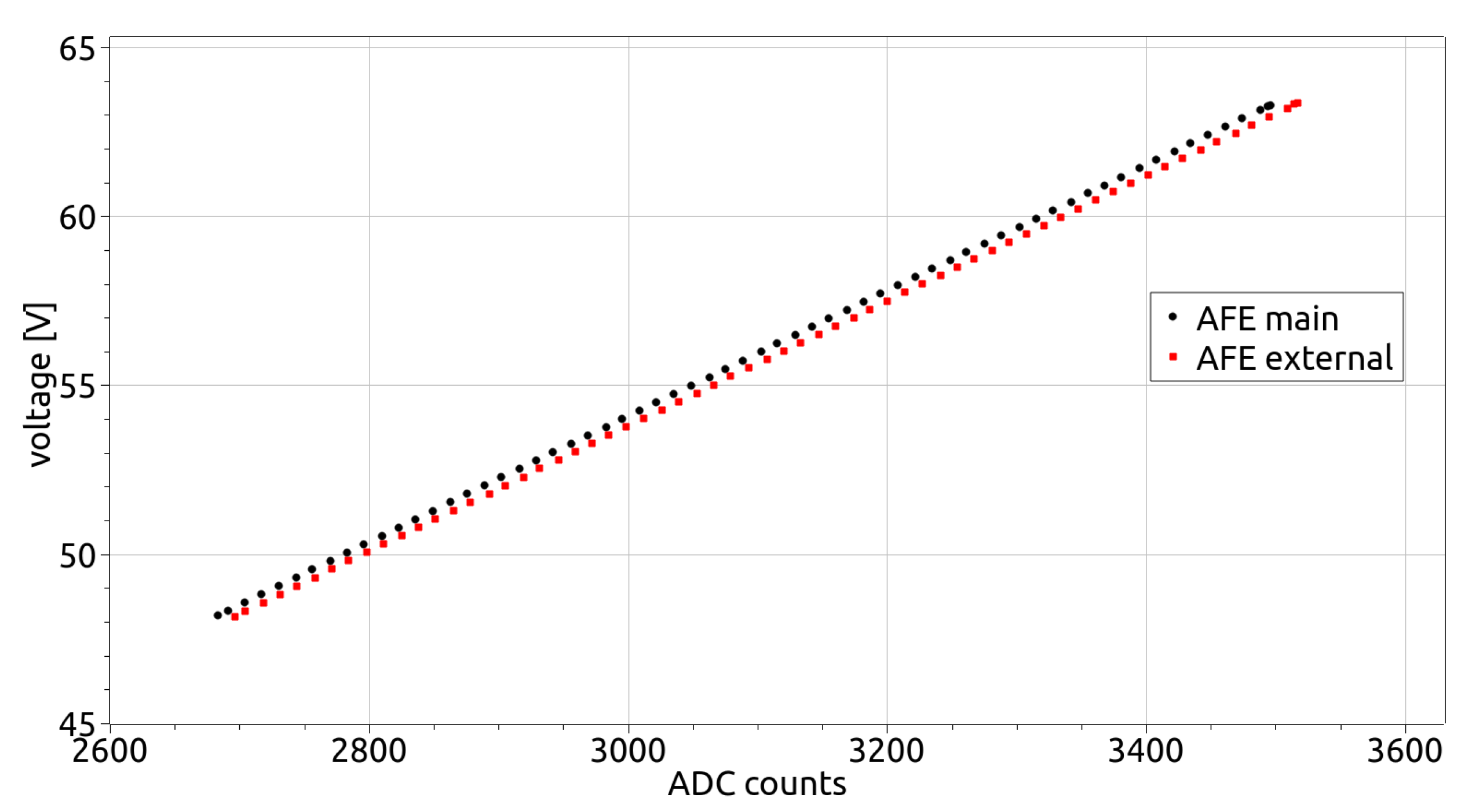
Figure 18.
AFE internal voltmeter calibration comparison between Main and External AFEs.
Figure 18.
AFE internal voltmeter calibration comparison between Main and External AFEs.
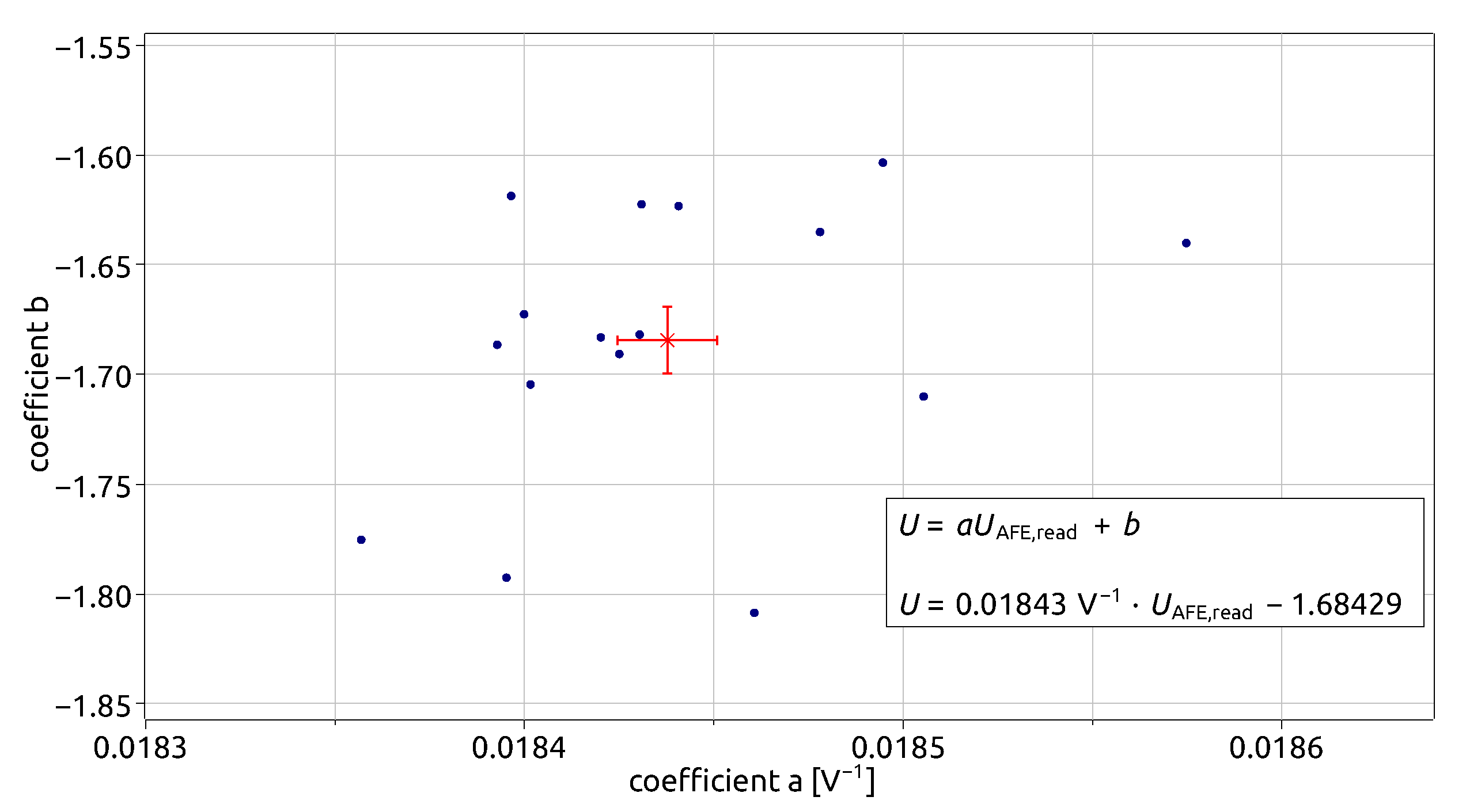
Figure 19.
Internal voltmeter calibration coefficient distribution. The scale is limited to a narrow range to show small differences in presented values. The average value is marked with a red marker.
Figure 19.
Internal voltmeter calibration coefficient distribution. The scale is limited to a narrow range to show small differences in presented values. The average value is marked with a red marker.
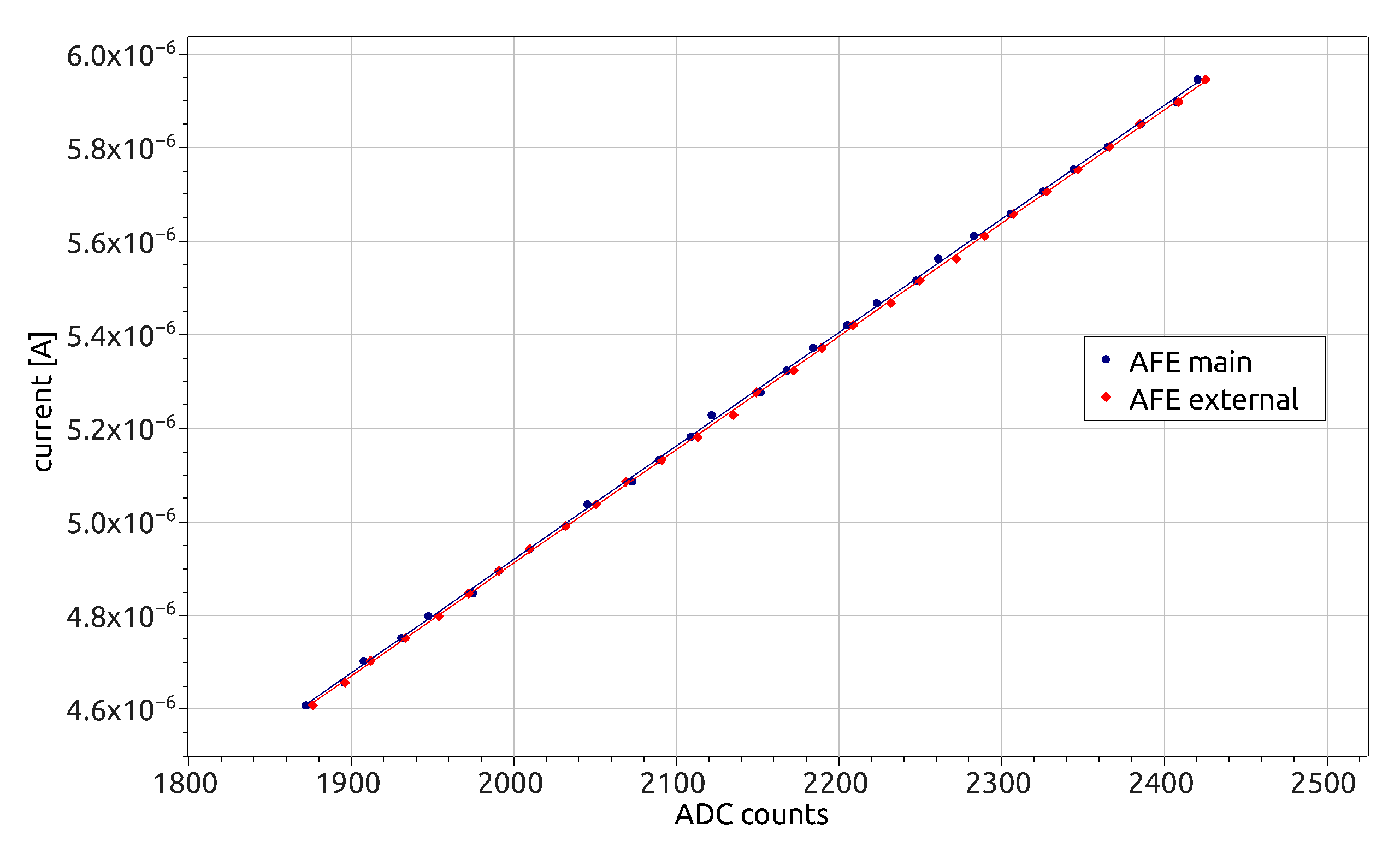
Figure 20.
Main and external AFE ammeter calibration. The scale is limited to a narrow range to show small differences in presented values.
Figure 20.
Main and external AFE ammeter calibration. The scale is limited to a narrow range to show small differences in presented values.
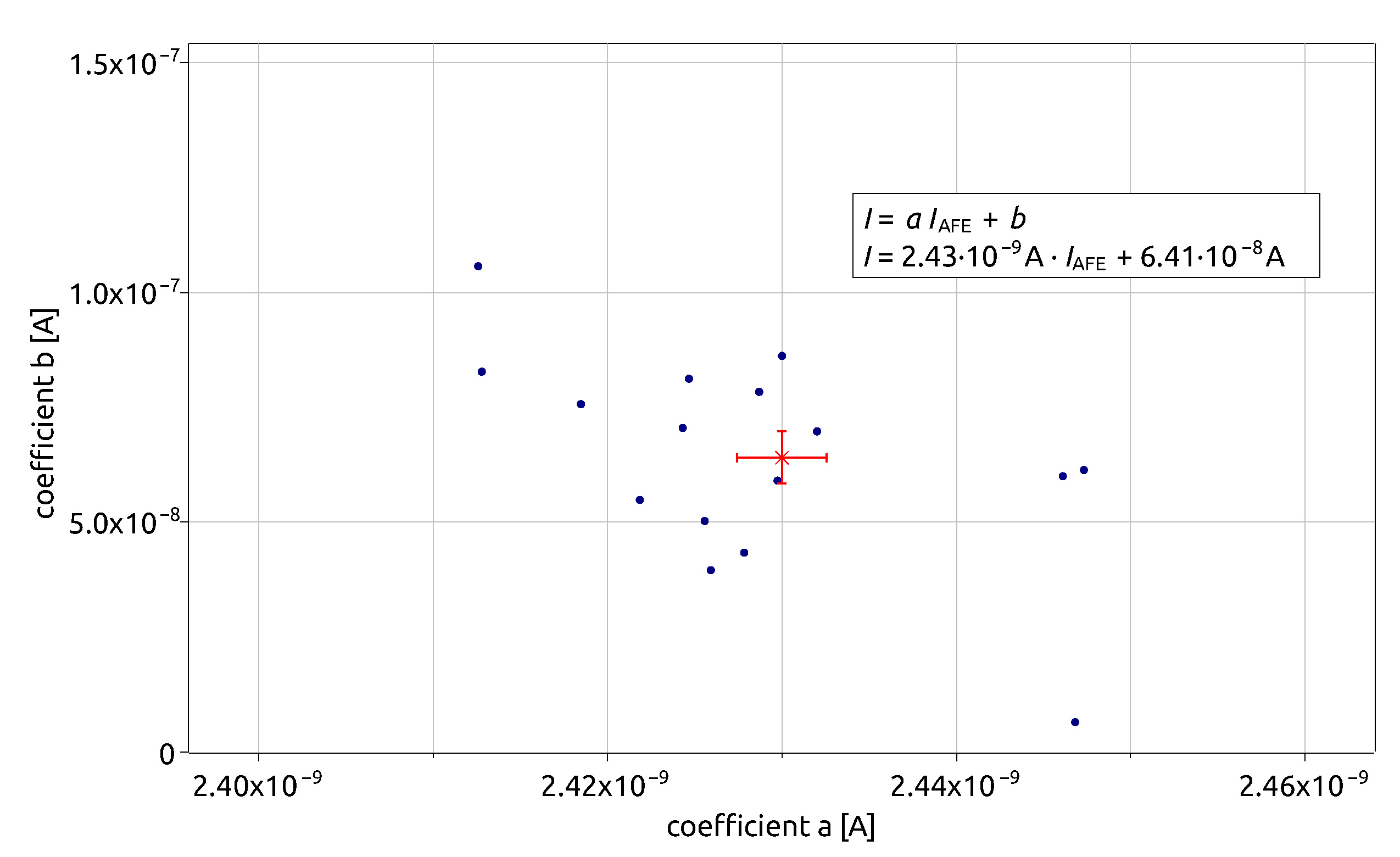
Figure 21.
AFE ammeter calibration coefficient distribution. The scale is limited to a narrow range to show small differences in presented values. The average value is marked with a red marker.
Figure 21.
AFE ammeter calibration coefficient distribution. The scale is limited to a narrow range to show small differences in presented values. The average value is marked with a red marker.
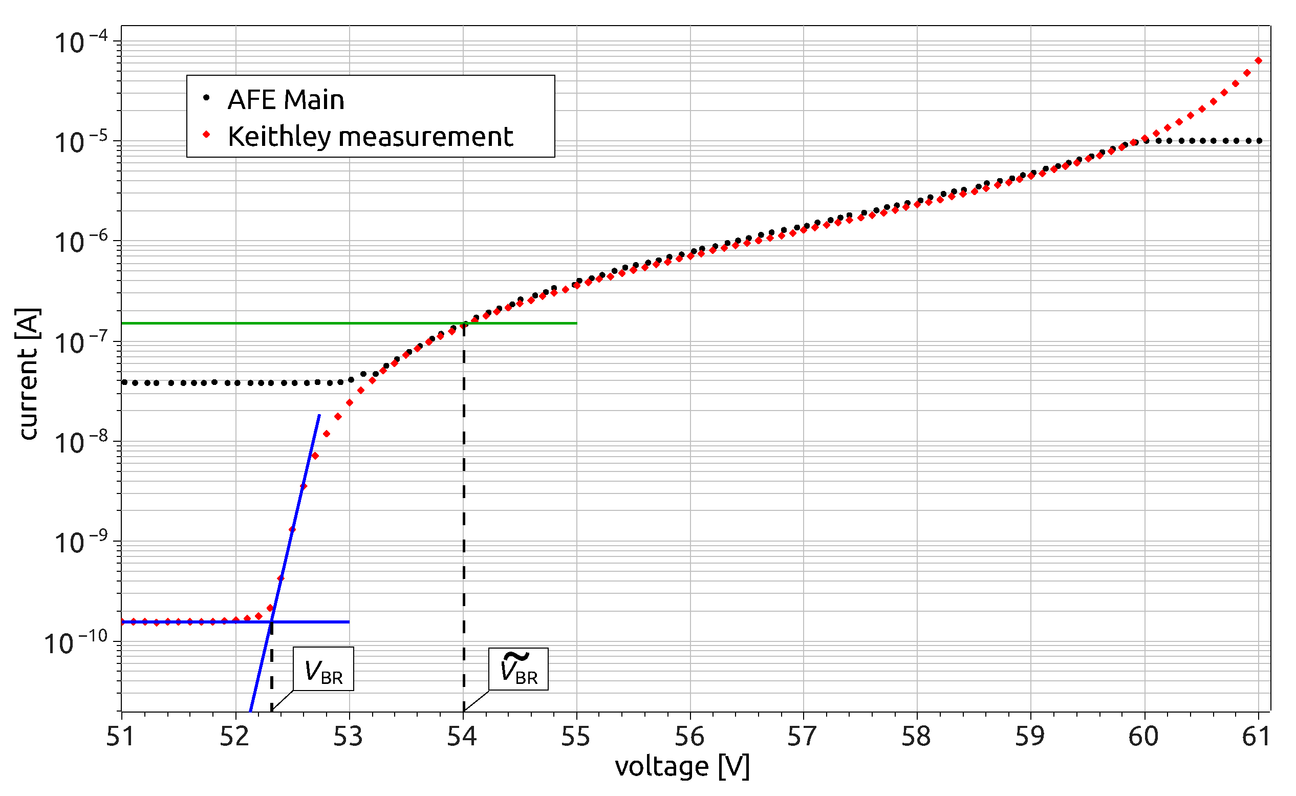
Figure 22.
Current—voltage characteristics measured using Keithley electrometer and AFE internal meters. The green line represents current level at which is determined. The intersection of the blue lines determines .
Figure 22.
Current—voltage characteristics measured using Keithley electrometer and AFE internal meters. The green line represents current level at which is determined. The intersection of the blue lines determines .
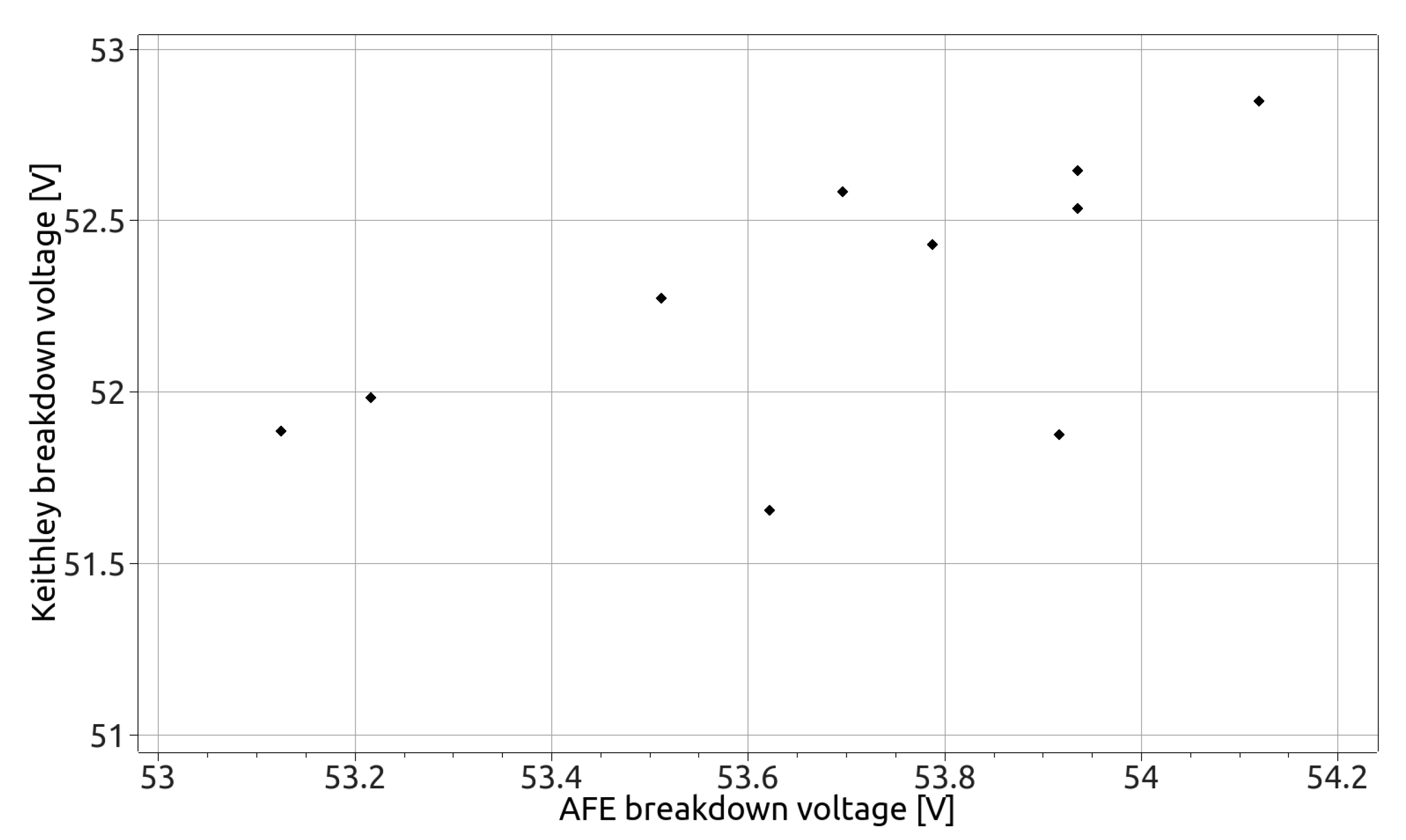
Figure 23.
Breakdown voltage (determined using Keithley meter) vs. operational breakdown voltage (determined using AFE meters).
Figure 23.
Breakdown voltage (determined using Keithley meter) vs. operational breakdown voltage (determined using AFE meters).
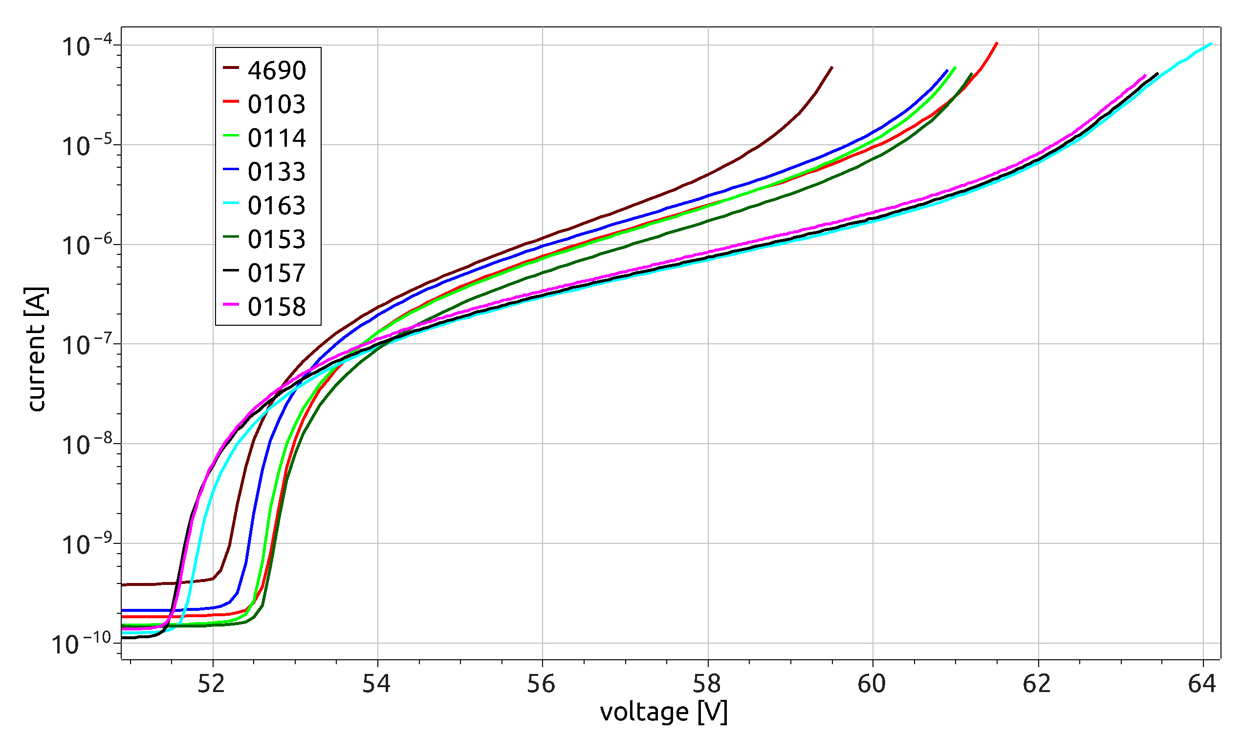
Figure 24.
Current–voltage characteristics for various SiMPs.
Figure 24.
Current–voltage characteristics for various SiMPs.
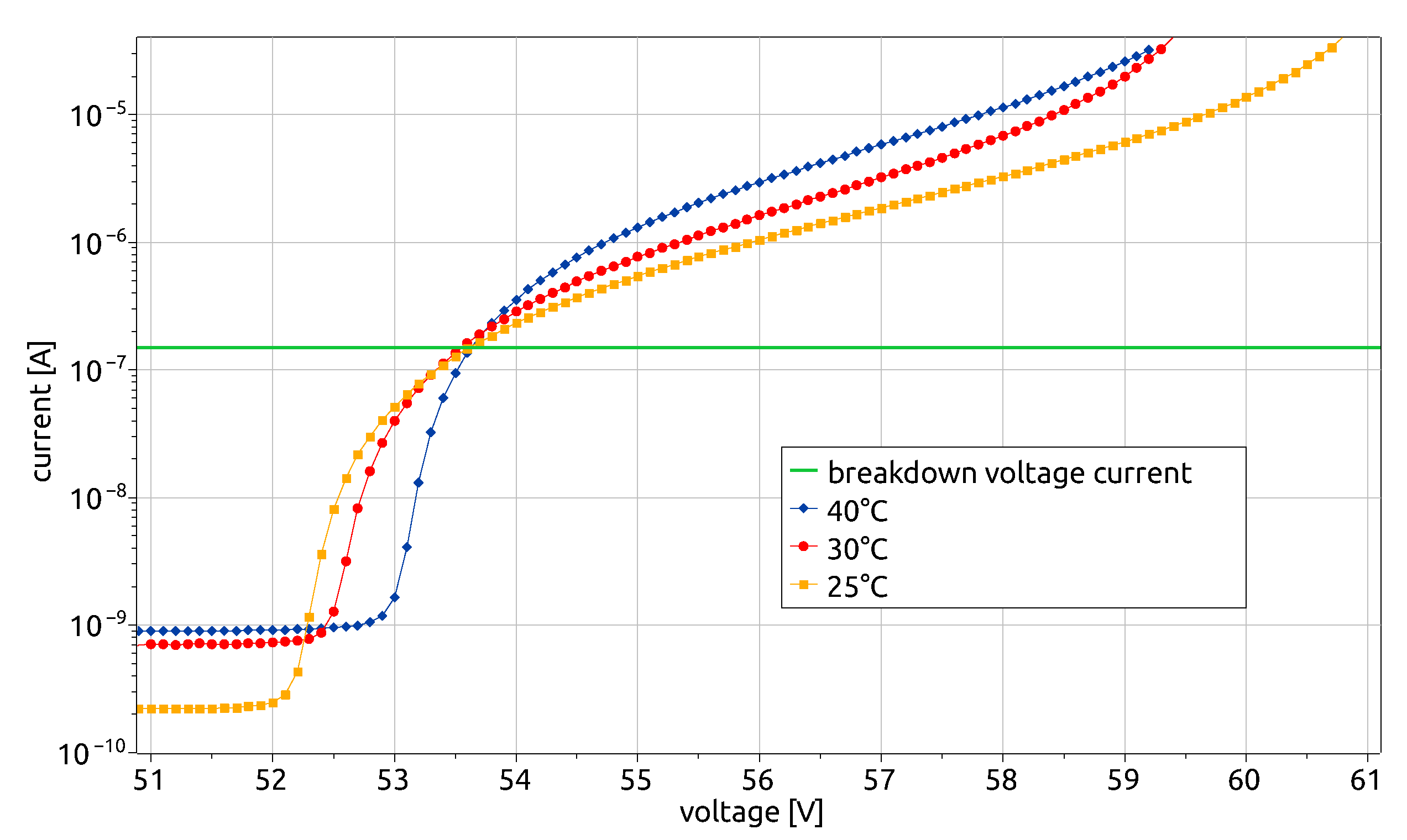
Figure 25.
Current—voltage characteristics of SiMP under different temperatures.
Figure 25.
Current—voltage characteristics of SiMP under different temperatures.
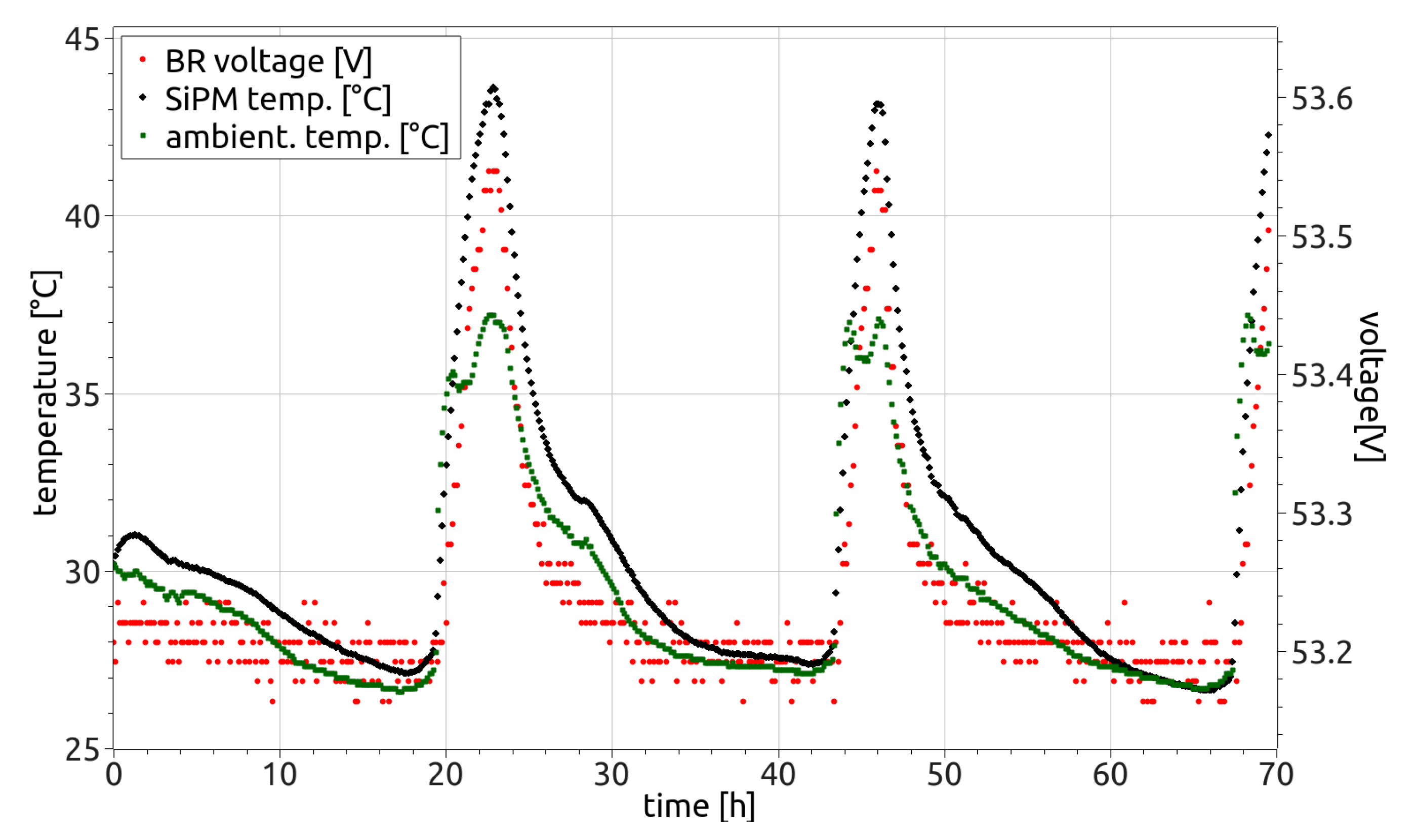
Figure 26.
Long-term correlation of the breakdown voltage , ambient temperature measured with a Keithley electrometer on the detector slab casing, and temperature measured by AFE near the SiPM. The ambient temperature was intentionally increased by placing the detector in sunlight during hot summer days. The calibration parameters of the AFE thermometer are taken from the vendor documentation.
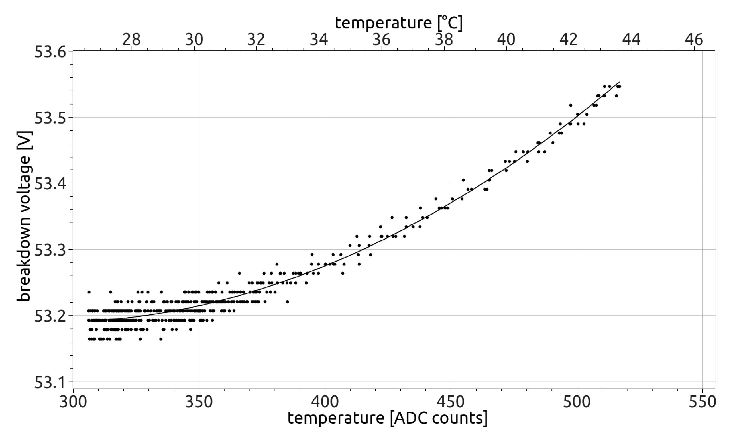
Figure 27.
Dependence of the breakdown voltage on the SiPM temperature measured by AFE. The calibration parameters of the AFE thermometer are taken from the vendor documentation.
Figure 27.
Dependence of the breakdown voltage on the SiPM temperature measured by AFE. The calibration parameters of the AFE thermometer are taken from the vendor documentation.
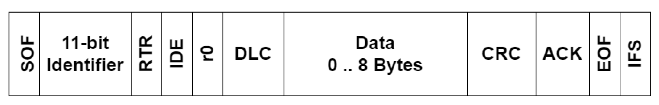
Figure 28.
Fields of Standard CAN Frame. A detailed description of every field can be found in [
21].
Figure 28.
Fields of Standard CAN Frame. A detailed description of every field can be found in [
21].
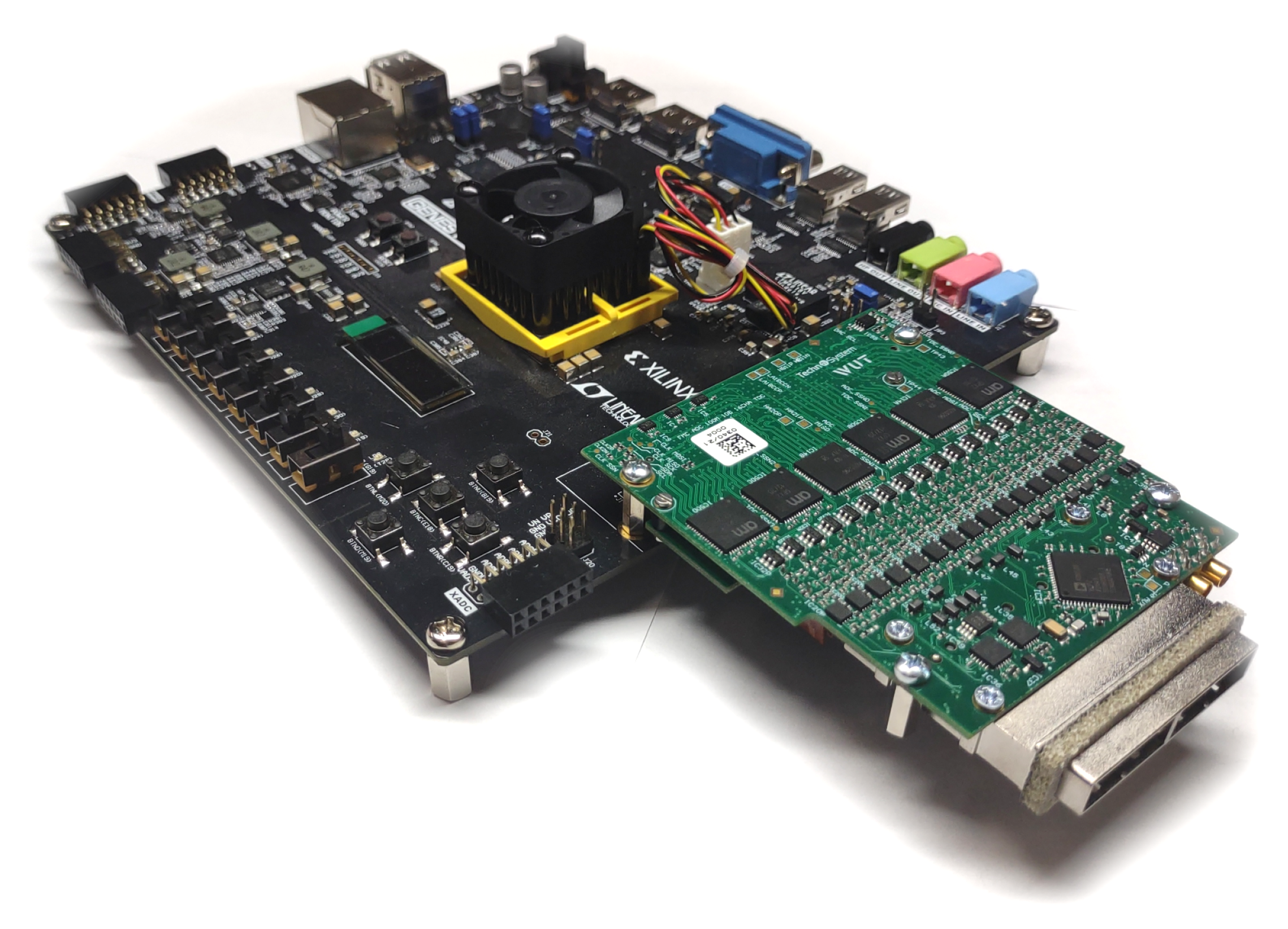
Figure 29.
Minimal MCORD DAQ testing setup using FMC ADC100M 10B TDC 16cha and Digilent Genesys 2.
Figure 29.
Minimal MCORD DAQ testing setup using FMC ADC100M 10B TDC 16cha and Digilent Genesys 2.
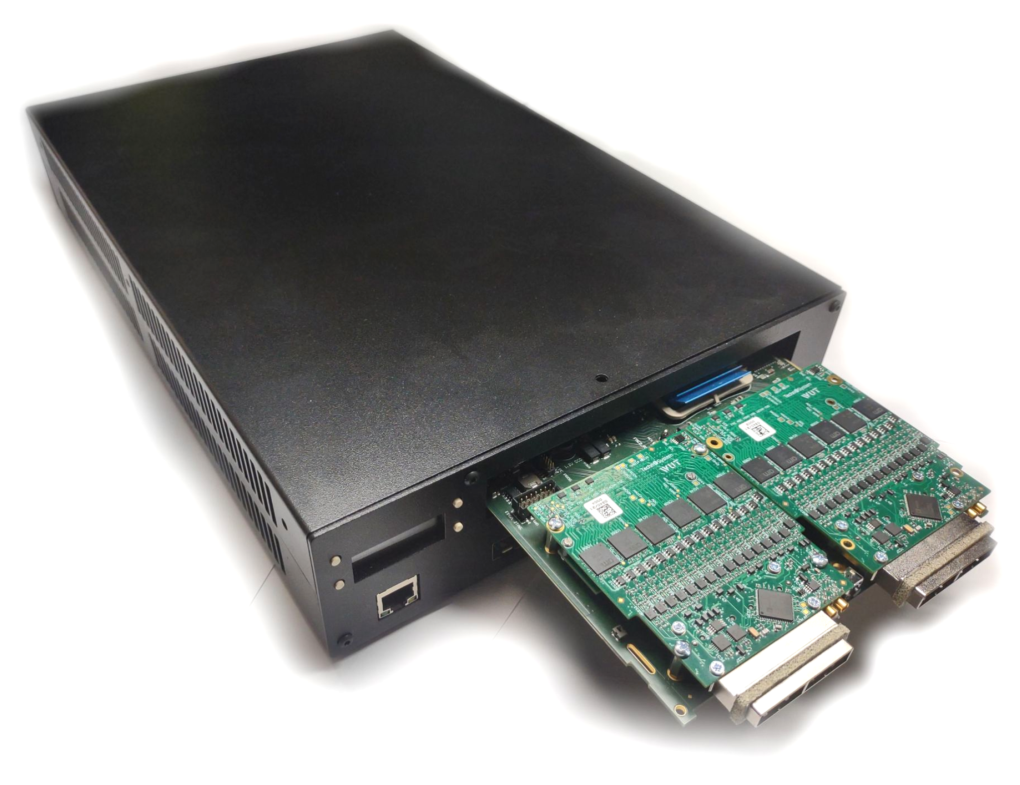
Figure 30.
Setup of 2 FMC–ADC–TDC modules (green electronic boards) mounted on AFCK board inside mTCA Chassis (black box). AFCK and modules are temporarily ejected for presentation/maintenance purposes.
Figure 30.
Setup of 2 FMC–ADC–TDC modules (green electronic boards) mounted on AFCK board inside mTCA Chassis (black box). AFCK and modules are temporarily ejected for presentation/maintenance purposes.
Figure 31.
AMC FMC Carrier Kintex (AFCK) [
24].
Figure 31.
AMC FMC Carrier Kintex (AFCK) [
24].
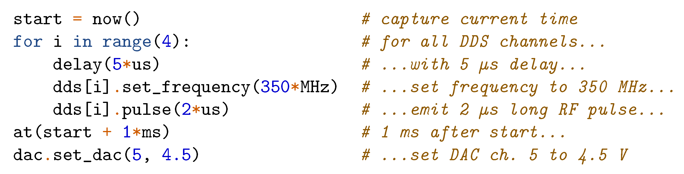
Figure 32.
Fragment of the experiment described in ARTIQ DSL.
Figure 32.
Fragment of the experiment described in ARTIQ DSL.
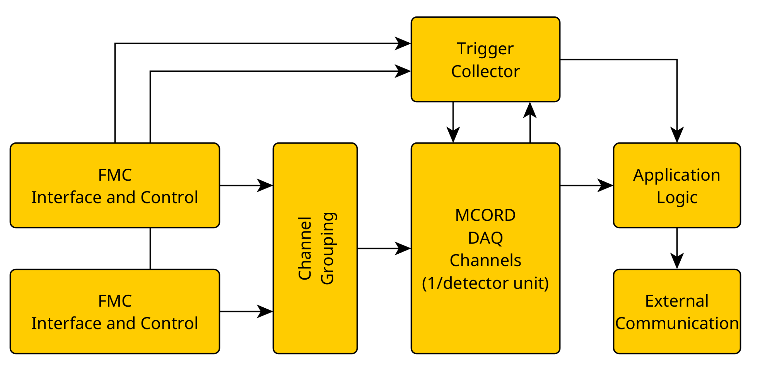
Figure 33.
General overview of MCORD DAQ Firmware for single-carrier application.
Figure 33.
General overview of MCORD DAQ Firmware for single-carrier application.
Figure 34.
ADC data flow.
Figure 34.
ADC data flow.
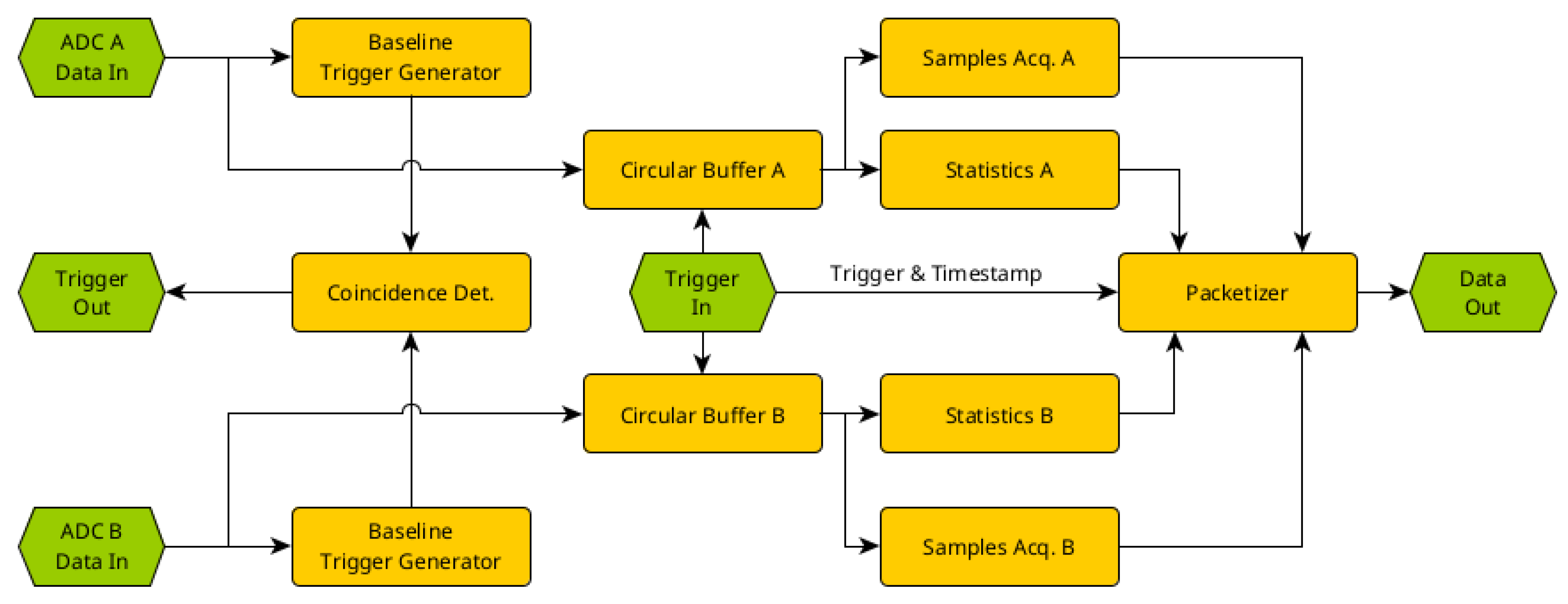
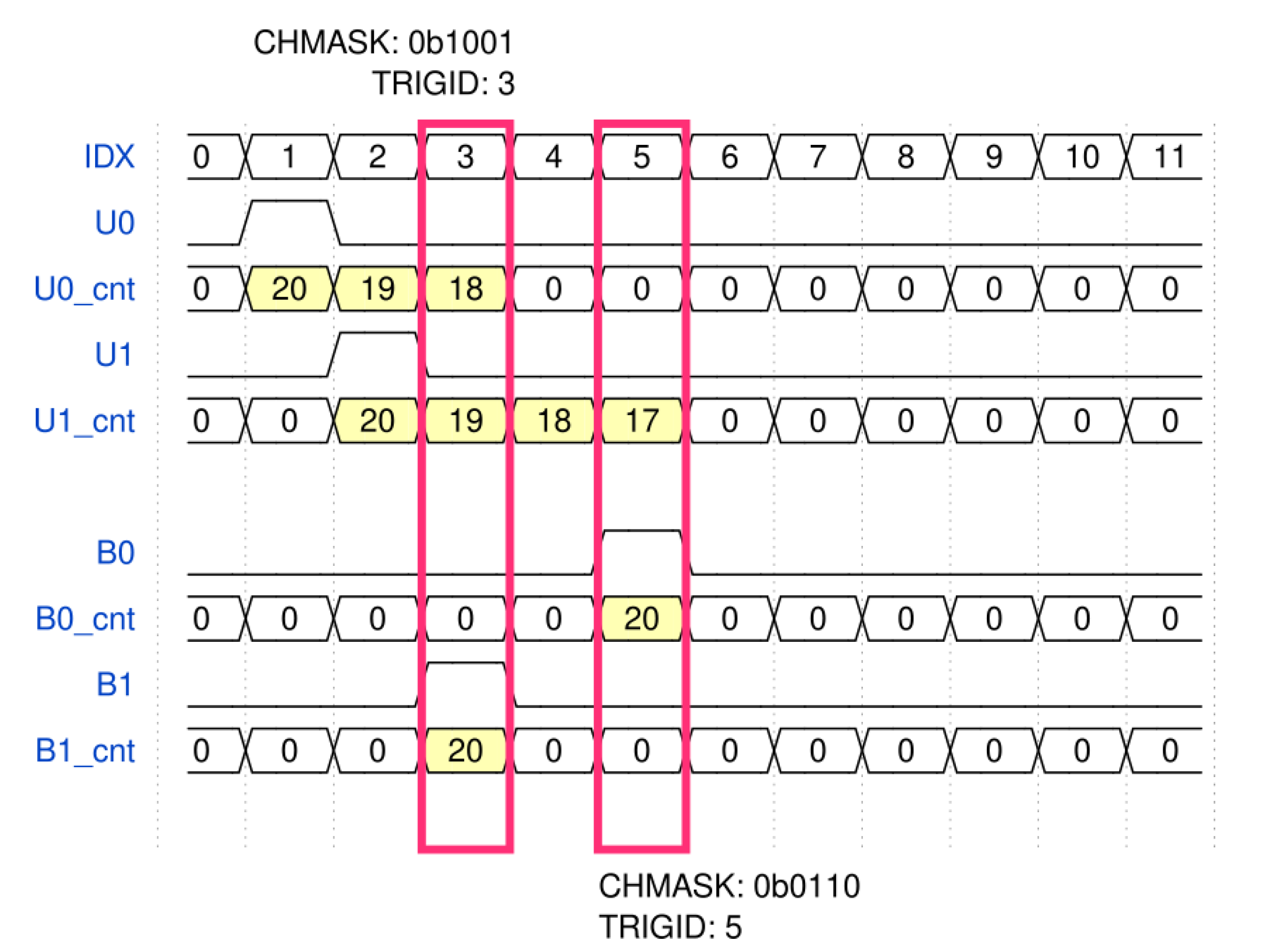
Figure 35.
Coincidence detection for single detector unit.
Figure 35.
Coincidence detection for single detector unit.
Figure 36.
TDC data flow.
Figure 36.
TDC data flow.
Figure 37.
Demonstration setup.
Figure 37.
Demonstration setup.
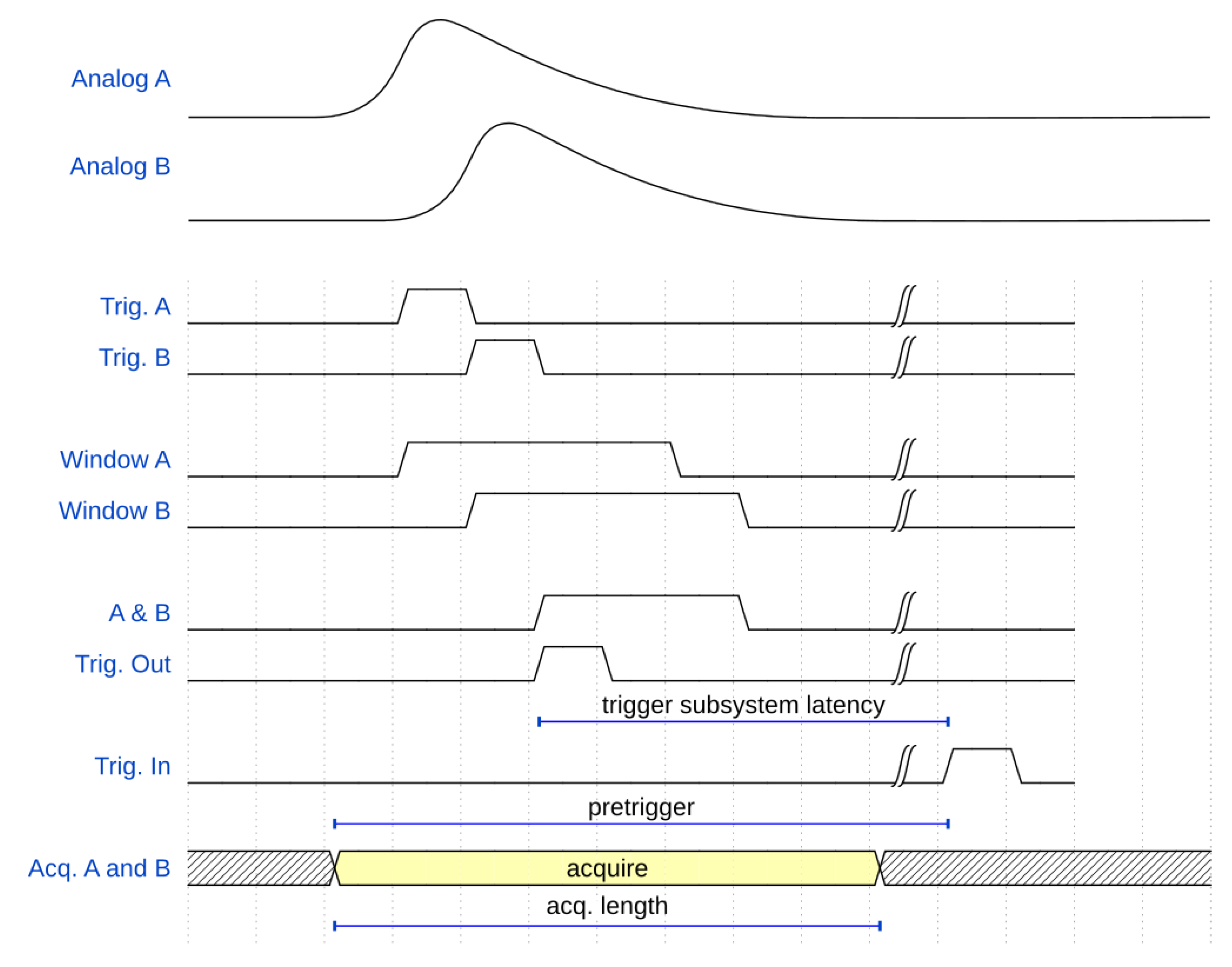
Figure 38.
Example data for triggering subsystem of demonstration application.
Figure 38.
Example data for triggering subsystem of demonstration application.
Table 1.
The relation between normal and operational breakdown voltages ( and , respectively), determined in this study. Values of breakdown voltage and current at operational voltage determined at the factory are presented for comparison. Last two rows present SiPMs from the second production batch.
| SiPM ID | [V] | [V] | [V] | [V] | [A] |
|---|
| 0101 | 53.93 | 52.64 | 1.29 | 52.43 | 0.566 |
| 0107 | 53.51 | 52.27 | 1.24 | 52.07 | 0.601 |
| 0110 | 53.12 | 51.88 | 1.23 | 51.67 | 0.589 |
| 0134 | 53.69 | 52.58 | 1.11 | 52.39 | 0.691 |
| 0137 | 54.12 | 52.84 | 1.27 | 52.63 | 0.552 |
| 0139 | 53.93 | 52.53 | 1.40 | 52.40 | 0.532 |
| 0145 | 53.21 | 51.98 | 1.23 | 51.78 | 0.604 |
| 0150 | 53.78 | 52.42 | 1.36 | 52.31 | 0.557 |
| 0181 | 53.91 | 51.87 | 2.04 | 51.64 | 0.283 |
| 0205 | 53.62 | 51.65 | 1.96 | 51.43 | 0.263 |
Table 2.
Definition of bits in the Control Register.
Table 2.
Definition of bits in the Control Register.
| Bit Number | Function |
|---|
| 0 | Enable/Disable DC/DC converter for SiPM A |
| 1 | Enable/Disable DC/DC converter for SiPM B |
| 2 | Enable/Disable signal path calibration pulses path for SiPM A |
| 3 | Enable/Disable signal path calibration pulses path for SiPM B |
Table 3.
List of CAN transactions for setting bits in Control Register.
Table 3.
List of CAN transactions for setting bits in Control Register.
| Function | Function Individual Code | Arguments | Return Data |
|---|
| Set bits in a Control Register | 0x0040 | Bits to set | – |
| Clear bits in a Control Register | 0x0041 | Bits to clear | – |
| Get bits in a Control Register | 0x0042 | – | Bit values in the Register |
Table 4.
CAN transaction for setting SiPM Voltage.
Table 4.
CAN transaction for setting SiPM Voltage.
| Function | Function Individual Code | Arguments | Return Data |
|---|
| Set voltage for SiPM A and B | 0x0012 | DAC binary values to set voltage for SiPM A (2 bytes) and SiPM B (2 bytes) | – |
Table 5.
List of CAN transactions for reading Voltage, Current, and Temperature values.
Table 5.
List of CAN transactions for reading Voltage, Current, and Temperature values.
| Function | Function Individual Code | Arguments | Return Data |
|---|
| Get ADC data Reg. 1 | 0x0010 | – | SiPM A Voltage (2 bytes), SiPM B Voltage (2 bytes), SiPM A Current (2 bytes) |
| Get ADC data Reg. 2 | 0x0011 | – | SiPM B Current (2 bytes), SiPM A Offset Voltage (2 bytes), SiPM B Offset Voltage (2 bytes) |
| Get temperature values | 0x0013 | – | SiPM A Temperature (2 bytes), SiPM B Temperature (2 bytes) |
Table 6.
CAN transaction for setting offset for SiPM signal path.
Table 6.
CAN transaction for setting offset for SiPM signal path.
| Function | Function Individual Code | Arguments | Return Data |
|---|
| Set digital resistance | 0x00A0 | 2 × RAW Digital Resistance values | – |
Table 7.
CAN transaction for reading AFE firmware version.
Table 7.
CAN transaction for reading AFE firmware version.
| Function | Function Individual Code | Arguments | Return Data |
|---|
| Get version | 0x0001 | – | Firmware version (6 bytes) |


 ,
, 


