Article

A Power-Gated 8-Transistor Physically Unclonable Function Accelerates Evaluation Speeds

Microsystems Group, School of Engineering, Newcastle University, Newcastle upon Tyne NE1 7RU, UK
*
Author to whom correspondence should be addressed.
J. Low Power Electron. Appl. 2023, 13(4), 53; https://doi.org/10.3390/jlpea13040053
Submission received: 17 August 2023 / Revised: 18 September 2023 / Accepted: 27 September 2023 / Published: 29 September 2023
(This article belongs to the Special Issue Ultra-Low-Power ICs for the Internet of Things Vol. 2)

Abstract

:
The proposed 8-Transistor (8T) Physically Unclonable Function (PUF), in conjunction with the power gating technique, can significantly accelerate a single evaluation cycle more than 100,000 times faster than a 6-Transistor (6T) Static Random-Access Memory (SRAM) PUF. The 8T PUF is built to swiftly eliminate data remanence and maximise physical mismatch. Moreover, a two-phase power gating module is devised to provide controllable power on/off cycles for the chosen PUF clusters in order to facilitate fast statistical measurements and curb the in-rush current. The architecture and hardware implementation of the power-gated PUF are developed to accommodate fast multiple evaluations of PUF Responses. The fast speed enables a new data processing method, which coordinates Dark-bit masking and Multiple Temporal Majority Voting (TMV) in different Process, Voltage and Temperature (PVT) corners or during field usage, hence greatly reducing the Bit Error Rate (BER) and the hardware penalty for error correction. The designs are based on the UMC 65 nm technology and aim to tape out an Application-Specific Integrated Circuit (ASIC) chip. Post-layout Monte Carlo (MC) simulations are performed with Cadence, and the extracted PUF Responses are processed with Matlab to evaluate the 8T PUF performance and statistical metrics for subsequent inclusion in PUF Responses, which comprise the novelty of this approach.

1. Introduction

1.1. Background

The Internet of Things (IoT) market is growing fast in annual revenue. However, this globally interconnected world poses a much more severe challenge to security. Due to the extremely resource-constrained nature of many IoT devices, e.g., wearables, lightweight security schemes and enhanced energy efficiency are consequently in great demand. To build a strong physical cyber-defence capability from the very start of the Integrated Circuit (IC) design [1], PUFs are promising hardware security primitives because they are easy to evaluate and physically hard to duplicate [2]. PUFs are functions that map Challenges to Responses through physically unclonable devices [2,3], and each PUF device is unique. Their uniqueness comes from the uncontrollable physical parameter mismatch generated in semiconductor fabrication. The proposed 8T PUF is derived from conventional 6T-SRAM. SRAM is an indispensable part of mainstream embedded designs because of its symmetric structure and mass entropy. The SRAM PUF was first proposed by Guajardo et al. [4] and Holcomb et al. [5], who discovered the intrinsically random start-up values of SRAM cells. Accordingly, these repeatable start-up values are the raw data for creating the Response of the PUF, and the address used to read them is the Challenge, as shown in Figure 2.
However, in a small number of SRAM cells, random logical states inevitably appear after every power-up due to negligible physical mismatch. They cause unreliable PUF readings, which cannot be tolerated for authentication. Moreover, some stable cells become unstable with the change in environmental conditions, such as temperature or supply voltage, because the physical mismatch in cells is affected, e.g., the threshold voltages of transistors.
One PUF application is extracting and regenerating Secret Keys. The raw data read from the PUF cells are the source for creating Secret Keys. The keys are normally extracted during manufacturing in a stable nominal temperature and voltage condition and regenerated in the field with various environmental conditions. Since no error can be tolerated for Secret Key application, there are some requisite techniques for identifying unstable PUF cells during manufacturing, such as Multiple Evaluation [6], TMV [6,7,8,9], Dark-bit masking [7,8,9,10], etc. Then, the stable cells can be used to derive the Secret Key for authentication. Whilst the keys are regenerated in the field, SRAM PUF is sensitive to environmental changes and ambient noise, which both cause bit errors. However, time is too limited to execute any aforementioned techniques to reduce errors. Thus, bit error correction techniques are vital, such as BCH codes [11], Hamming codes [12], etc. For error correction and its required PUF entropy, the hardware overheads increase exponentially with the growth in error numbers [13]. This is unsuitable for lightweight IoT applications.

1.2. Main Contributions

Two fundamental circuits are built in this work: one is the custom 8T PUF in Figure 1a; the other is the two-phase power gating cell in Figure 1b. A single-phase power gating cell is also implemented for comparison, as shown in Figure 1c. Based on these circuits, a power-gated 8-Transistor (8T) PUF architecture presented in Figure 2 is developed to alleviate some of the aforementioned issues. This power gating structure can also be utilised with the other bistable PUFs to improve PUF performance. The main contributions are listed below:
  • The custom 8T PUF facilitates fast statistical measurements and improves security: The 8T PUF maximises physical mismatch and eliminates data retention swiftly for high-speed evaluations and countering security attacks [14,15,16,17,18]. It does not require a special process for high-density SRAM manufacturing and can be fabricated in the same process as microcontrollers (MCUs). Fast statistical measurements can be performed on this platform to extract raw PUF bits. These raw bits are then processed and marked onto a bitmap to identify the PUF cell instability. These unstable bits, which are discarded in the references, can be used for True Random Number generation or as part of the PUF Response [19,20,21,22].
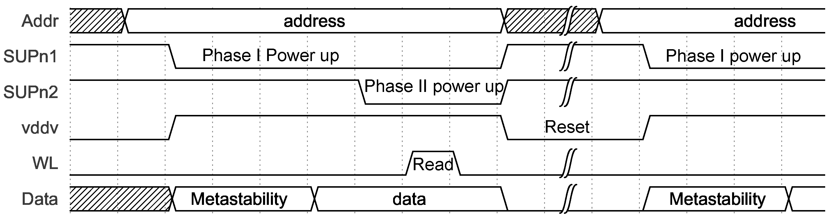
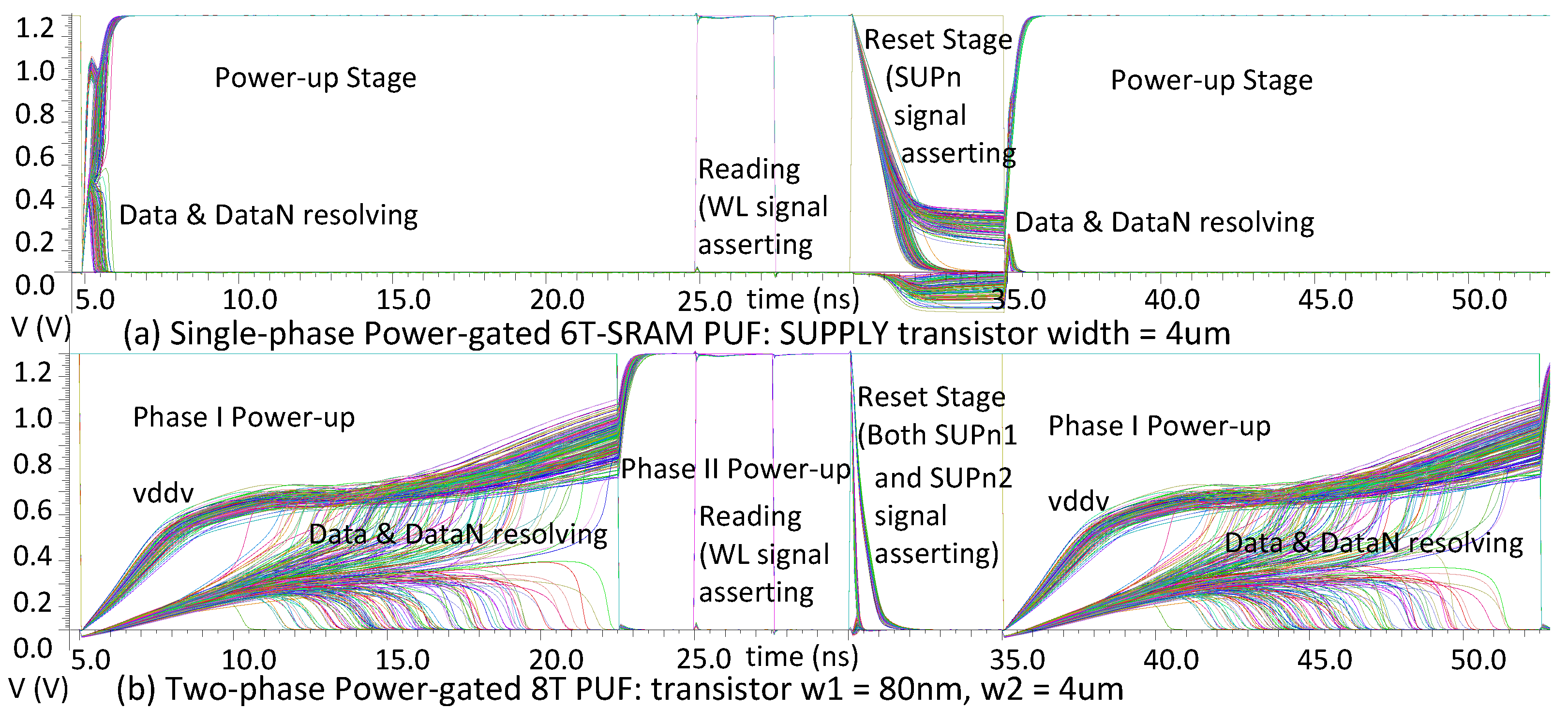
  • Two-phase power gating improves PUF performance and security whilst saving energy and delaying ageing: This newly developed power-switching process includes three stages:
    • Reset stage: The reset stage drops the virtual power supply (vddv), quickly drains the remaining current and eliminates retained data.
    • Phase I power-up stage: Phase I slowly powers up the chosen PUFs to prolong the metastability-resolving process in the hope of reducing EMI and crosstalk amongst PUF cells [23].
    • Phase II power-up stage: Finally, phase II speeds up the voltage ramp-up process.
    In addition, different combinations of power gating parameters can curb the in-rush current, thus shielding it from side channel attacks, e.g., Differential Power Analysis (DPA) [14,15]. Moreover, the 8T PUF cells are partitioned into rows, and only the chosen rows will be powered up during the reading process. Besides saving energy proportionally, PUF cells without a power supply cannot be read out and are protected from security attacks. Furthermore, power gating can delay the transistor ageing effect.
  • A new data processing method marks out most errors: The high-speed measurements not only reduce the time needed for the enrolment phase in manufacturing but also enable multiple evaluations in the key regeneration phase. Since the positions of the unstable PUF cells drift away in different voltage or temperature corners, and extreme corners cause more unstable PUF cells, TMV plus Dark-bit masking in nominal conditions [7,8,9] is insufficient. We propose a new data processing method here. First, during manufacturing, Multiple TMV under nominal conditions and extreme corners are used to mark out unstable readings and flipped readings as Dark bits onto a bitmap. Then, during field usage, the Dark bits are discarded first and followed by the regeneration of Secret Keys using fast TMV. Finally, with a significantly reduced number of error bits remaining, an error correction technique with a lower hardware penalty will be applied. When the BER drop close to 0%, the hardware penalty for error correction can be reduced significantly. The stability levels of PUFs are also recorded on the bitmap. These unstable readings can be used further for True Random Number generation or as part of the PUF Response.

1.3. State of the Art and Related PUF Works

Before starting a new silicon-based PUF design, the implementation method needs to be considered first. The silicon-based PUFs can be implemented in an ASIC or a Field-Programmable Gate Array (FPGA). Since FPGAs have ready-to-use resources and can be purchased off-the-shelf, many early PUF works are based on FPGAs [2,3,4]. However, ASIC-based PUFs can offer far more energy and have a cost-efficient design, which is crucial for lightweight IoT devices [8,9,24,25,26,27,28,29,30,31,32,33,34]. However, FPGA-based PUFs [35,36,37,38,39,40,41] are indispensable parts for applications which are not area or energy sensitive but time sensitive instead. In addition, FPGA is a feasible platform for assessing PUF design methods and performance. There are several novel FPGA-based bistable PUF works [36,37,38,39,40,41], which we intend to implement in our test chip with the power gating method to compare the metastable behaviour and PUF performance.
There are several PUF applications [42,43,44,45] that previously applied the power gating method, but their purposes and implementations are different to this approach. Maes et al. [42] implemented power-gated PUF blocks for further investigation. Xu et al. [43] utilised the random duration of multiple power gating to replace voltage control so as to induce failure patterns to determine the Data Retention Voltage (DRV). In comparison, our design diminishes data retention swiftly for high-speed evaluation. Although with a different purpose, this research and its predecessor [46] have clarified that “a strong DRV fingerprint is correlated with power-up tendency”. This substantiates that the stability or instability degrees of PUF cells come from their innate physical mismatch. However, it can be seen that 40 μ s is not enough to eliminate retention data at 25 C. In 2020, a 2D power gating scheme to relieve an enhancement–enhancement (EE) SRAM PUF from short-circuit currents and also to protect PUF data from attacks was presented by Liu et al. [44]. However, there was no consideration of the major power gating parameters, such as the SLEEP transistor design [47], power distribution network [48], etc. This scheme also has a half-selected cell problem, which requires additional peripheral circuits to lower the extra energy consumption.

1.4. Paper Structure

The remainder of this paper is organised as follows. Section 2 describes the power-gated PUF architecture, the 8T PUF design, the two-phase power gating implementation and a new data processing method combining Multiple TMV and Dark-bit masking. Section 3 firstly analyses the power gating parameters, then compares the power-gated 8T PUF behaviour with the 6T PUF, and lastly discusses the importance of a thorough reset for PUF applications. Section 4 measures the processed data for a PUF property comparison. Finally, Section 5 concludes the main contributions and outlines the ongoing work and future plan.

2. Power-Gated PUF Architecture and Design Methods

An example architecture of a power-gated PUF array is illustrated in Figure 2. This architecture consists of some general SRAM function blocks in grey, a 2 kilo-bit power-gated PUF array and two functional blocks, i.e., a Control block and a Data Processing block. The two function blocks will be implemented and evaluated in due course.
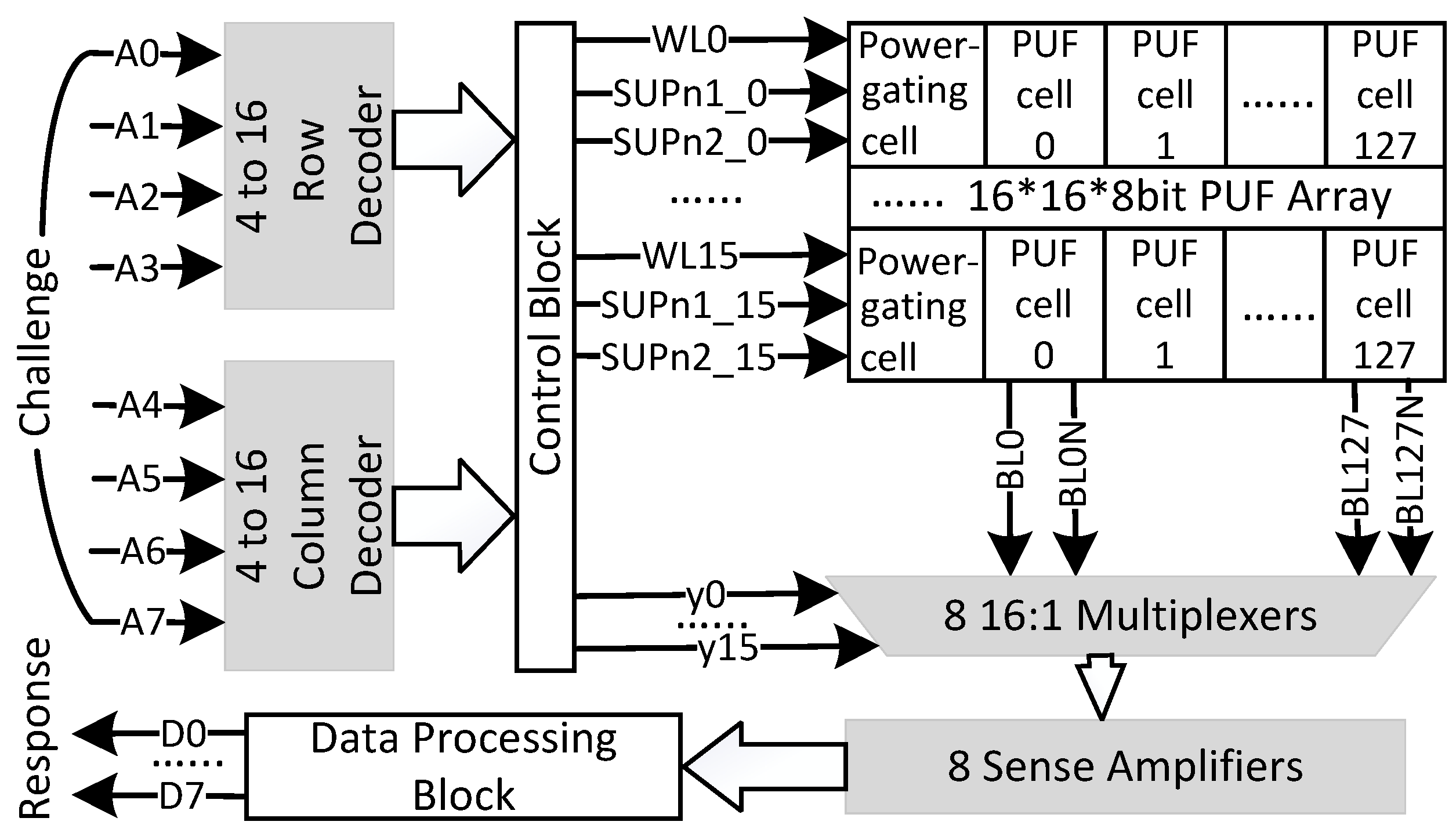
  • Challenge–Response pair (CRP): The 8-bit address inputs are the PUF Challenges, and the 8-bit corresponding data outputs are the PUF Responses. Together, they form a Challenge–Response pair (CRP).
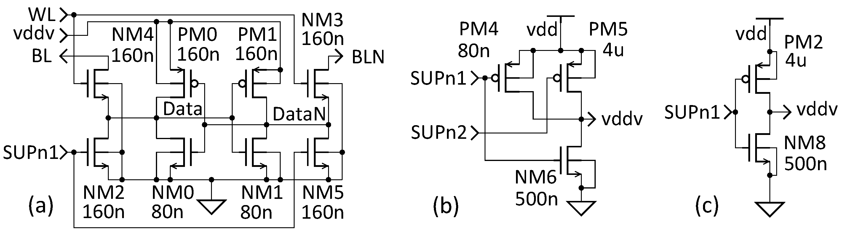
  • PUF array: In the PUF array, there are 128 PUFs in a row gated by a power gating cell. Since the main purpose of power gating is facilitating fast evaluations by switching the power supply, the general term SLEEP for normal power gating is replaced by SUPPLY in this work.
  • Control block: The switching activity is controlled by the Control block. Apart from passing the decoded higher 4-bit address to choose an 8-bit word from 16:1 multiplexers, it generates SUPn1, SUPn2 and WL (Word Line) signals from the decoded lower 4-bit address. Once a PUF row is chosen by the lower 4-bit address, the SUPn1 signal is discharged to ‘0’ to switch on the power supply. After Data are settled down, the SUPn2 will be discharged to ‘0’, and WL will be asserted to ‘1’ in sequence for a reading process. Then, in the Reset stage, both SUPn1 and SUPn2 signals are asserted to ‘1’. There will be no power supply to the PUF cells, and the data will be discharged to ‘0’. The protocol of the two-phase power gating method is shown in Figure 3.
  • Data Processing block: The Data Processing block is there to evaluate the raw read-out bits and marking out different stability levels of each PUF cell. Using TMV under nominal or various voltage and temperature conditions is to sift the unstable or flipped bits to achieve a lower Bit Error Rate (BER).
The input vectors and the output vectors of multiple PUF arrays can be concatenated to match the PUF entropy requirement. The parameters of this architecture, e.g., the type of PUF cell, the number of rows or columns, word width, etc., can be altered for various purposes or implemented in different fabrication techniques. It is worth noting that with larger PUF array dimensions, the sizes of SUPPLY transistors need to be evaluated. The driven ability of SUPn1 and SUPn2 signals needs to be improved.
The design is implemented with UMC 65 nm technology. The layout of one test circuit is partly illustrated in Figure 4. It includes rows of two-phase power-gated 8T PUFs on the left-hand side and rows of single-phase power-gated 6T-SRAM PUFs on the right-hand side for comparison. Each row has 128 PUF cells.

2.1. 8-Transistor PUF Design

A distinctive feature of the 8T PUF is preparing a clean status for the next power-on cycle with a high reset speed. This clean status means attackers cannot read out any retention data. Unlike some 8T SRAM designs [49,50] concentrating on improving the write margin and dealing with the opposite requirements for read stability and write ability, this 8T PUF abandons the write function and keeps only the SRAM read ability. The physical parameter mismatch, which affects SRAM stability, is actually a vital feature of PUFs. Since mismatch amongst transistors increases with the scaling down the physical size, the 8T PUF uses the smallest transistor to maximise the mismatch. An 8T PUF can be fabricated by the same process as MCUs, so a special process for high-density SRAM is not needed.
The 8T PUF cell shown in Figure 1a stems from conventional 6T-SRAM [51]. Four transistors, namely PM0, PM1, NM0 and NM1, make up two cross-coupled inverters for storing data. The unique PUF readings predominantly come from the threshold voltage mismatch among these transistors. After powering up, the mutual input and output nodes, i.e., Data and DataN, both reach a metastable state [52], at which time the outputs of two cross-coupled inverters are lingering between logical ‘0’ and ‘1’, then cross it and settle in one of these stable states. NM4 and NM3 are access transistors. They connect the internal nodes Data and DataN to bit lines BL and BLN. In addition, two NMOS transistors NM2 and NM5 are designed to rapidly discharge the Data and DataN nodes during the reset stage with both SUPn1 and SUPn2 signals asserting. As a result, the reset time can be shortened by 5 orders of magnitude, i.e., from 120 microseconds to 1 nanosecond, hence facilitating high-rate PUF evaluation. Furthermore, no data remanence can be exploited by attackers [53,54]. The PUF layouts were implemented symmetrically. During the evaluations, it is shown that a tiny bias of layout influences the proportion of the ones and zeros of the PUF readings. With two additional transistors, the area cost of the 8T PUF is 13.2% more than its 6T-SRAM PUF counterpart, which was implemented for comparison as shown in Figure 4.

2.2. Two-Phase Power Gating Method and Design

Originally, the power gating technique was introduced to reduce leakage, which is independent of the transistor switching activity and thus lessens power dissipation. This design eliminates the leakage current from unchosen PUF rows, so the energy consumption is roughly proportional to the chosen PUF percentage. In the two-phase power gating method, the power gating cells switch the chosen rows of PUF cells on and off in three stages: a reset stage, phase I power-up and phase II power-up. First and foremost, this enables fast statistical evaluations, which improve PUF performance. Secondly, this method facilitates different combinations of power gating parameters in hardware implementation, so that the in-rush current can be curbed by adjusting these parameters. The flattened currents provide a method against side channel attacks. Moreover, PUF rows without power supply cannot be read out and are protected from security attacks.
Conventional power gating is conducted via a SLEEP transistor to enable a power or ground connection [47]. Figure 1b shows the single-phase power gating cell is operated via a PMOS transistor PM2 as a SUPPLY transistor to switch power on/off and an NMOS transistor NM8 for fast resetting. As illustrated in Figure 1c, the two-phase power gating cell employs two PMOS transistors as SUPPLY transistors for two-stage power switching and an NMOS transistor NM6 for resetting. In the test circuits, each power gating cell controls the power supply of a row of 128 PUF cells. The reset transistor NM6 quickly drains the remaining current and drops vddv to 0 V. Since a smaller transistor curbs the drain current and the vddv output, the two-phase power gating exploits this to generate a gentle voltage incline with a smaller SUPPLY transistor PM4 in phase I and create a steep slope of vddv using a larger SUPPLY transistor PM5 in phase II. Consequently, the metastability resolving time in phase I is lengthened in the hope of minimum mutual disturbance amongst PUF cells. Meanwhile, if all PUF cells start metastability in a very short period of time, the in-rush current will be significant due to all the cross-coupled transistors in 8T PUF cells being in saturation mode. The prolonged phase I is able to flatten the current peak as well. Afterwards, phase II takes control and increases vddv swiftly. The sizes of two SUPPLY transistors and the time duration of the two phases need to be evaluated to obtain the best trade-off. This will be discussed in the evaluation part in Section 3.1.

2.3. Multiple TMV and Dark-Bit Masking

In some previous methods combining TMV with Dark-bit masking [7,8,9], TMV cannot eliminate the unstable bits in different environmental conditions, and the Dark-bit mismatch increases bit errors more than 10-fold during field usage. This is because the physical mismatch, e.g., the threshold voltages, vary under different voltages or temperatures. Hence, some stable cells become unstable and vice versa. However, there are some cells that even change their bias tendency and flip their readings. PUF cells with flipped readings cannot be distinguished by TMV under nominal condition.
We introduce a Multiple TMV method with additional TMV thanks to the high-speed evaluation enabled by the proposed design and architecture. During manufacturing, the golden reading is extracted using TMV in the nominal condition first. Then, by comparing the TMV results at all worst corners with the golden reading, any flipped bits and unstable bits are marked as Dark bits. Afterwards, while the Secret Key regenerates in the field, the marked-out Dark bits will be eliminated from the raw data first. Then TMV will be executed next, and the unstable bits at this moment are the error bits. Then, these error bits will be corrected with the error correction technique with a lower hardware penalty. The simulation results show that the BER can drop to 0%, which is presented in Section 4.

3. Evaluations and Results Analyses

Due to the sensitivity of bistable PUFs, e.g., the 8T PUF and the SRAM PUF, many aspects of parameter mismatch count for the PUF stability. Although the layouts were implemented symmetrically to avoid human-made bias, the physical parameters still exhibit variations. For this reason, post-layout simulation is a much more accurate way to evaluate the sizes of SUPPLY transistors and measure PUF performance, such as uniqueness, robustness and randomness. For various evaluation purposes, different simulation methods were executed with corresponding test circuits.

3.1. Power Gating Parameter Evaluation

A DC sweep and post-layout transient simulations were performed to evaluate the size of SUPPLY transistors for a cluster of 128 PUF cells and the corresponding behaviour of the PUF cells.
For two-phase power gating, the phase one SUPPLY transistor PM4 must be small enough to prolong the metastability process. Meanwhile, the phase two SUPPLY transistor PM5 should be large enough to supply power to 128 PUF cells quickly. As presented in Figure 5, there is a roughly linear relationship between the SUPPLY transistor width and the approximate value of the vddv plateau while metastability resolves. There is also a nearly quadratic dependence between the SUPPLY transistor width and the time duration for vddv to reach 1.2 V or the metastability resolving time duration. Hence, by varying the size of the SUPPLY transistor, the metastability resolving time can be manipulated.
Phase I SUPPLY transistor widths of 80 nm to 320 nm and phase II SUPPLY transistor widths of 1 μ m to 4 μ m were picked to evaluate various combinations of two-phase power gating. Figure 6 illustrates the comparison of the current peaks of different signal edges in different combinations of SUPPLY transistors whilst power gating a 128-bit PUF. It can be seen that a higher power-up current corresponds to a larger SUPPLY transistor. The phase II current also relates to the vddv value at the start point of phase II. The energy consumption of a PUF cell for each reading cycle exhibits minimal variation, i.e., from 5.7 fJ to 6.2 fJ. These adjustable power-up currents can limit the in-rush current and be exploited further as a candidate against side channel attacks. In our design, the SUPPLY transistor combination of 80 nm for PM4 and 4 μ m for PM5 is implemented to emphasise the prolonged PUF metastability-resolving process and the rapid reset process.
The power consumption of a power-gated PUF array is proportional to the chosen PUF percentage, in addition to the power consumption of the power-gating cells. The post-layout simulation results show that the power consumption is about 36.5% when only a quarter of PUF rows are enabled. For example, a row of 128 8T PUFs consumes 954 fJ in an array of four PUF rows, which consume 2.613 pJ under the same conditions. The dynamic power of one two-phase power gating cell is about 812.5 aJ.

3.2. Power-Gated PUF Behaviour

To examine the PUF behaviour of 8T PUFs, post-layout Monte Carlo simulations with a Gaussian distribution of transistor threshold voltages were carried out under nominal conditions, i.e., a supply voltage of 1.2 V, an ambient temperature of 27 C and a Typical–Typical (TT) process corner. The test circuit includes a row of 128 two-phase power-gated 8T PUFs and a row of 128 single-phase power-gated 6T-SRAM PUFs on the right-hand side for comparison.
The 128-run Monte Carlo simulation results illustrate the different power-up and reset behaviours of PUF cells, as shown in Figure 7. In Figure 7a, with a 4 μ m width SUPPLY transistor, the vddv of single-phase power gating reaches 1.2 V in roughly 1 ns, whilst quickly resolving the metastability of inside node pairs, i.e., Data and DataN. In contrast, Figure 7b illustrates that vddv reaches around 0.7 V in 5 ns and lingers for about 4 ns, then gradually climbs up towards 1.2 V at phase I power-up with the SUPPLY transistor width of 80 nm. Following this, with a 4 μ m width SUPPLY transistor, phase II starts from 22.5 ns and swiftly increases vddv to 1.2 V in around 1 ns with the help of the 80 nm SUPPLY transistor. It can be seen that the low start-up voltages in phase I lengthen the metastability resolving time of 8T PUFs. Simultaneously, Data and DataN start wrestling while vddv is ramping up slowly, then escape out of metastability and tend to their distinct logical status in various resolving times due to their intrinsically varied physical parameters. These opposite tendencies of Data and DataN resemble the random PUF behaviour in real circuits.
After powering up, the WL signal asserts at 25 ns for data reading. Finally, in the reset stage, PUF cells are powered down. The remaining currents are drained away quickly from the 8T PUF cells within 1 ns. However, the traditional 6T-SRAM PUFs still have data retention, which not only affects the initial states of Data and DataN pairs in the following cycles but also can be targeted by attackers. It is worth noting that with the technology scaling down from 90 nm to 65 nm, the reset period for the same 6T-SRAM design lengthens from 5 μ s to 120 μ s, as listed in Table 1.

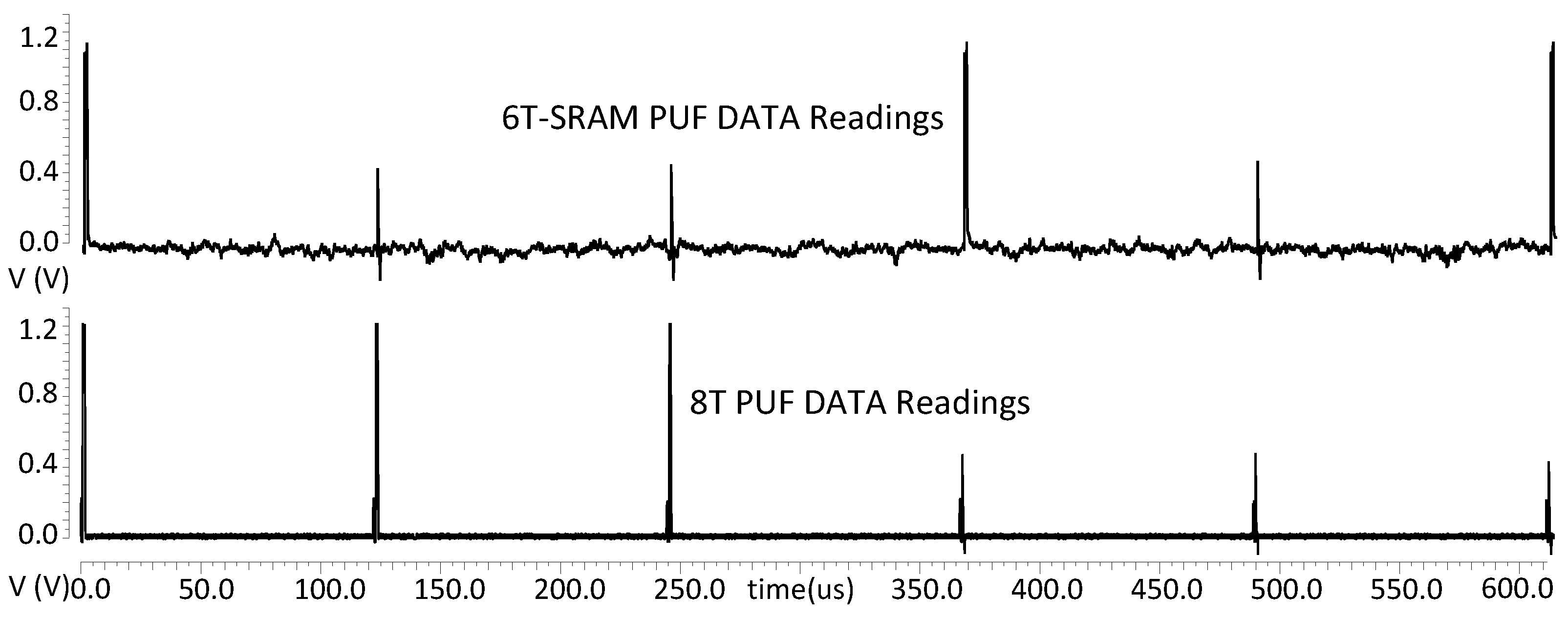
3.3. Reset Period and Effect

Without resetting thoroughly, the assessment of the PUF characteristics can be misguiding. One piece of evidence is that with the data remanence, the under-reset 6T-SRAM PUF readings do not change in more than 200,000 runs of a Monte Carlo simulation compared to the 8T PUF. This creates a deceptive deduction that the 6T-SRAM PUF cells are 100% stable in nominal conditions [57]. However, if the reset time duration is prolonged to 120 μ s with 65 nm technology, the simulation results show that the stability of the thoroughly reset 6T-SRAM PUF will be affected in the same way as the 8T PUF, as illustrated in Figure 8. Long duration transient simulations were conducted with intensified noise. In these simulations, the 8T PUF cell, with the help of two discharging NMOS transistors, can reset two internal data nodes to the absolute values below 10 mV within 1 ns, while the 6T-SRAM PUF can barely achieve the same reset level even in 100 μ s.
This reset issue has been overlooked because most research does not switch power at such high frequencies, as listed in Table 1. Consequently, the longer power-off periods result in a better reset quality under the same conditions.

4. 8-Transistor PUF Performance Measurements

To assess the PUF performance, 5G transient noise, including thermal noise, flicker noise, shot noise, etc., was added to the post-layout Monte Carlo simulations because all 8T PUF cells and 6T-SRAM PUF cells were stable in nominal conditions without any external noise. For the two-phase power gating SUPPLY transistors, an 80 nm width was chosen for phase I, and 4 μ m was chosen for phase II. Meanwhile, the 6T-SRAM PUF was examined under the same conditions for comparison. In addition to nominal conditions, the design was evaluated under different PVT corners, i.e., temperatures from −40 C to 85 C and supply voltages from 0.8 V to 1.6 V, and the process corners included Slow–Slow (SS), Fast–Fast (FF) etc. For quantitative evaluation, clusters of 2048 PUF cells were read out for 100 power on–off cycles of 60 ns. This resembles 100 times the same Challenge. The 100 2048-bit read-out strings are the PUF Responses. Furthermore, the PUF clusters imitate different PUF devices. With a thorough reset, these PUF characteristics are able to be assessed with post-layout simulations. The intensive multiple simulations here aim to examine the PUF properties to prepare for prototype chip fabrication, so the extracted data were then processed with Matlab to acquire PUF robustness, uniqueness, randomness, etc. The results were compared with some prior work in Table 2. It is worth noting that the works [8,9,25,58,59,60,61] are ASIC-based measurements, and only [62] and this work include simulation-based evaluations. In fact, post-layout simulations are very resource and time consuming, so only a few works, e.g., [62], can extract data from schematic-based simulations.
By comparing this work with state-of-the-art designs, it is shown to satisfy the basic PUF requirements and can be evaluated as a PUF. From Table 2, it can be seen that some of the latest designs [44,59,60,61] improve the native stability of PUFs and achieve the native BER very close to 0%. Ref. [44] realises a 0% stabilised BER with relatively high mask ratios and energy consumption per bit, while [59,60,61] utilises a novel circuit implementation. This work tries to reach the same level of performance with high-frequency evaluations enabled by the power-gated 8T PUF structure. Since the post-layout simulation is extremely time and resource consuming, there are only a few previous works that attain the same level of results by simulation, e.g., the results of [62] are extracted from schematic-based simulations. The main achievement of the proposed design and structure is the speed, which saves time and hence conserves the total power consumption, etc.

4.1. Uniformity

For PUF uniformity, the proportion of ones and zeros of the 8T PUF readings should be evenly distributed. Our results of stable zeroes are 46.22% and stable ones are 46.06%.

4.2. Robustness: Intra-Distance and BER

For an ideal PUF cell, the Responses to the same Challenge should always be the same. However, the existence of unstable cells makes this impossible. Thus, the intra-distance, which is the Hamming distance between bit strings of the Responses from repeated measurements of the same PUF, is used to evaluate the PUF robustness. To minimise the area overheads for error correction in the key regeneration phase, the intra-distance is expected to be close to zero. By comparing every pair of two Response bit strings and adding up the total numbers of different bits, the intra-distances are calculated. The average intra-distance of all the simulated 8T PUF groups is 1.45%.
Under nominal conditions, the average percentage of total unstable bits in 20 groups of 2048 8T PUF cells is 7.71%; the raw BER is 1.17%. The corresponding BER of the worst corner is 12.21%. Most of the unstable readings can be fixed by the Data Processing block using TMV, which can be visualised in the golden bitmap generated in the key enrolment phase. For example, in the golden bitmap shown in Figure 9, squares with different colours represent the statistical results of the PUF stability, i.e., white indicates stable ‘0’, black squares show stable ‘1’ and different grey shades present the degree of bias of the cells. Most impressively, the worst corner BER can be decreased to 0% with Dark-bit masking coordinated with TMV in the worst voltage and temperature corners and in the field. The mask ratio is 21.78%. As a result, the hardware penalty for error correction is minimised.

4.3. Uniqueness: Inter-Distance

Since PUFs are the hardware sources for identifying individual devices or generating Secret Keys, the extracted information from each PUF should be unique. The fractional Hamming distance was computed between different PUF devices. In order to successfully identify each PUF device, this value should be close to 50%. In the experiments, the Response bit strings of different PUF clusters were compared to calculate the inter-distance. The average inter-distance of the 20 8T PUF clusters is 50.67%.

4.4. Randomness

Firstly, the Applied Auto-correlation Function (ACF) was used to analyse the spatial correlations among 64 groups of 2048 8T PUFs. The result is 0.0315, which is close to zero, within the 95% confidence bound. This indicates a low spatial correlation of the 8T PUFs based on the physical extraction from the layout design. Then, the randomness of 64 groups of 2048 8T PUFs was assessed with the NIST SP 800-22 [63] statistical test suite. The NIST results are listed in Table 3. The simulation results passed most of the tests. However, the randomness generated by the simulator has limitations, especially for the large amount of data which is required by both the ACF and NIST test suite. Moreover, this practical simulation method is time and resource consuming. A test chip for facilitating on-chip statistical experiments is under development to improve the evaluation efficiency and verify the PUF behaviour in the real world.

5. Conclusions and Future Work

In this paper, the design, architecture and evaluation of a rapid reset 8T PUF utilising the power gating technique are presented. Its purpose is to enhance PUF stability and minimise the hardware penalty for error corrections. The design can apply on–off power cycles repeatedly to PUF clusters to facilitate fast multiple evaluations for extracting the bias probability of PUF cells. The ultra-fast speed enables TMV in different voltage and temperature corners or in the field. Dark-bit masking based on these extracted data can reduce the BER to close to zero in experiments. In the design, an SRAM-based 8T PUF cell with the ability to eliminate data retention is built, and a two-phase power gating method is devised and evaluated. Besides switching the power supply swiftly and saving power, the power-up process can be manipulated via varying the power gating method and parameters so as to decrease the interference between sensitive PUF cells and limit the in-rush current during power-up. Consequently, PUF stability and security are enhanced. In addition, the clean and fast reset makes it possible for swift and accurate PUF measurements either in simulation or in a fabricated silicon chip. The 8T PUF characteristics, including robustness, uniqueness and randomness, are thus qualitatively confirmed.
Future work will include quantitative evaluations of the 8T PUF performance on various PVT corners and assessments of different power gating settings. The extracted unstable degrees of PUF cells will be post-processed and added to the PUF Response to increase its entropy. In addition to this, a test chip is currently being fabricated. Afterwards, the fabricated test chip will enable on-chip statistical experiments, which serve as a platform to extract analogue secrets. Finally, the differences in the power-gated 8T PUF’s entropy compared to its 6T-SRAM PUF counterpart will be assessed, measured and reported.

Author Contributions

Conceptualisation, A.B.; methodology, Y.Z. and A.B.; circuit design, Y.Z.; circuit simulation, Y.Z.; validation, Y.Z.; software, Y.Z.; formal analysis, Y.Z. and A.B.; resources, A.Y.; data curation, Y.Z.; writing—original draft preparation, Y.Z.; writing—review and editing, A.B and A.Y.; visualisation, Y.Z.; supervision, A.B. and A.Y. All authors have read and agreed to the published version of the manuscript.

Funding

This research received no external funding.

Institutional Review Board Statement

Not applicable.

Informed Consent Statement

Not applicable.

Data Availability Statement

Not applicable.

Conflicts of Interest

The authors declare no conflict of interest.

Abbreviations

The following abbreviations are used in this manuscript:
8T8-Transistor
PUFPhysically Unclonable Function
6T6-Transistor
SRAMStatic Random-Access Memory
TMVTemporal Majority Voting
PVTProcess, Voltage and Temperature
BERBit Error Rate
ASICApplication Specific Integrated Circuit
IoTInternet of Things
ICIntegrated Circuit
MCUMicrocontroller
vddvvirtual power supply
DPADifferential Power Analysis
FPGAField-Programmable Gate Array
CRPChallenge–Response Pair
DRVData Retention Voltage
WLWord Line
TTTypical–Typical
SSSlow–Slow
FFFast–Fast
CMOSComplementary Metal Oxide Semiconductor
ACFApplied Autocorrelation Function

References

  1. Verbauwhede, I. Security Adds an Extra Dimension to IC Design: Future IC Design Must Focus on Security in Addition to Low Power and Energy. IEEE Solid-State Circuits Mag. 2017, 9, 41–45. [Google Scholar] [CrossRef]
  2. Gassend, B.; Clarke, D.; Van Dijk, M.; Devadas, S. Silicon physical random functions. In Proceedings of the 9th ACM Conference on Computer and Communications Security, Washington, DC, USA, 18–22 November 2002; pp. 148–160. [Google Scholar]
  3. Gassend, B.; Clarke, D.; Van Dijk, M.; Devadas, S. Controlled physical random functions. In Proceedings of the 18th Annual Computer Security Applications Conference, Las Vegas, NV, USA, 9–13 December 2002; pp. 149–160. [Google Scholar]
  4. Guajardo, J.; Kumar, S.S.; Schrijen, G.J.; Tuyls, P. FPGA intrinsic PUFs and their use for IP protection. In Cryptographic Hardware and Embedded Systems-CHES 2007: 9th International Workshop, Vienna, Austria, September 10–13; Proceedings 9; Springer: Berlin/Heidelberg, Germany, 2007; pp. 63–80. [Google Scholar]
  5. Holcomb, D.E.; Burleson, W.P.; Fu, K. Initial SRAM state as a fingerprint and source of true random numbers for RFID tags. In Proceedings of the Conference on RFID Security, Malaga, Spain, 10–13 April 2007; Volume 7, No. 2. p. 1. [Google Scholar]
  6. Bhargava, M.; Cakir, C.; Mai, K. Reliability enhancement of bi-stable PUFs in 65nm bulk CMOS. In Proceedings of the 2012 IEEE International Symposium on Hardware-Oriented Security and Trust (HOST), San Francisco, CA, USA, 3–4 June 2012; pp. 25–30. [Google Scholar]
  7. Armknecht, F.; Maes, R.; Sadeghi, A.R.; Sunar, B.; Tuyls, P. Memory leakage-resilient encryption based on physically unclonable functions. In Towards Hardware-Intrinsic Security: Foundations and Practice; Springer: Berlin/Heidelberg, Germany, 2010; pp. 135–164. [Google Scholar]
  8. Mathew, S.K.; Satpathy, S.K.; Anders, M.A.; Kaul, H.; Hsu, S.K.; Agarwal, A.; Chen, G.K.; Parker, R.J.; Krishnamurthy, R.K.; De, V. 16.2 A 0.19 pJ/b PVT-variation-tolerant hybrid physically unclonable function circuit for 100% stable secure key generation in 22 nm CMOS. In Proceedings of the 2014 IEEE International Solid-State Circuits Conference Digest of Technical Papers (ISSCC), San Francisco, CA, USA, 9–13 February 2014; pp. 278–279. [Google Scholar]
  9. Satpathy, S.K.; Mathew, S.K.; Suresh, V.; Anders, M.A.; Kaul, H.; Agarwal, A.; Hsu, S.K.; Chen, G.K.; Krishnamurthy, R.K.; De, V.K. A 4-fJ/b delay-hardened physically unclonable function circuit with selective bit destabilization in 14-nm trigate CMOS. IEEE J. Solid-State Circuits 2017, 52, 940–949. [Google Scholar] [CrossRef]
  10. Satpathy, S.K.; Mathew, S.K.; Li, J.; Koeberl, P.; Anders, M.A.; Kaul, H.; Chen, G.K.; Agarwal, A.; Hsu, S.K.; Krishnamurthy, R.K. 13fJ/bit probing-resilient 250K PUF array with soft darkbit masking for 1.94% bit-error in 22nm tri-gate CMOS. In Proceedings of the ESSCIRC 2014-40th European Solid State Circuits Conference (ESSCIRC), Venice, Italy, 22–26 September 2014; pp. 239–242. [Google Scholar]
  11. Bose, R.C.; Ray-Chaudhuri, D.K. On a class of error correcting binary group codes. Inf. Control 1960, 3, 68–79. [Google Scholar] [CrossRef]
  12. Hamming, R.W. Error detecting and error correcting codes. Bell Syst. Tech. J. 1950, 29, 147–160. [Google Scholar] [CrossRef]
  13. Bösch, C.; Guajardo, J.; Sadeghi, A.R.; Shokrollahi, J.; Tuyls, P. Efficient helper data key extractor on FPGAs. In Cryptographic Hardware and Embedded Systems–CHES 2008: Proceedings of the 10th International Workshop, Washington, DC, USA, 10–13 August 2008; Proceedings 10; Springer: Berlin/Heidelberg, Germany, 2008; pp. 181–197. [Google Scholar]
  14. Kocher, P.; Jaffe, J.; Jun, B. Differential power analysis. In Advances in Cryptology—CRYPTO’99: Proceedings of the 19th Annual International Cryptology Conference, Santa Barbara, CA, USA, 15–19 August 1999; Proceedings 19; Springer: Berlin/Heidelberg, Germany, 1999; pp. 388–397. [Google Scholar]
  15. Rührmair, U.; Xu, X.; Sölter, J.; Mahmoud, A.; Koushanfar, F.; Burleson, W. Power and timing side channels for PUFs and their efficient exploitation. Cryptol. Eprint Arch. 2013, 476–492. [Google Scholar]
  16. Rührmair, U.; Sölter, J.; Sehnke, F.; Xu, X.; Mahmoud, A.; Stoyanova, V.; Dror, G.; Schmidhuber, J.; Burleson, W.; Devadas, S. PUF modeling attacks on simulated and silicon data. IEEE Trans. Inf. Forensics Secur. 2013, 8, 1876–1891. [Google Scholar] [CrossRef]
  17. Halderman, J.A.; Schoen, S.D.; Heninger, N.; Clarkson, W.; Paul, W.; Calandrino, J.A.; Feldman, A.J.; Appelbaum, J.; Felten, E.W. Lest we remember: Cold-boot attacks on encryption keys. Commun. ACM 2009, 52, 91–98. [Google Scholar] [CrossRef]
  18. Anagnostopoulos, N.A.; Arul, T.; Rosenstihl, M.; Schaller, A.; Gabmeyer, S.; Katzenbeisser, S. Attacking SRAM PUFs using very-low-temperature data remanence. Microprocess. Microsyst. 2019, 71, 102864. [Google Scholar] [CrossRef]
  19. Wang, Y.; Liang, H.; Wang, Y.; Yao, L.; Yi, M.; Huang, Z.; Lu, Y. A reconfigurable PUF structure with dual working modes based on entropy separation model. Microelectron. J. 2022, 124, 105445. [Google Scholar] [CrossRef]
  20. Della Sala, R.; Scotti, G. Exploiting the DD-Cell as an Ultra-Compact Entropy Source for an FPGA-based Re-Configurable PUF-TRNG Architecture. IEEE Access 2023, 11, 86178–86195. [Google Scholar] [CrossRef]
  21. Maiti, A.; Nagesh, R.; Reddy, A.; Schaumont, P. Physical unclonable function and true random number generator: A compact and scalable implementation. In Proceedings of the 19th ACM Great Lakes symposium on VLSI, Boston Area, MA, USA, 10–12 May 2009; pp. 425–428. [Google Scholar]
  22. Baturone, I.; Román, R.; Corbacho, Á. A Unified Multibit PUF and TRNG based on Ring Oscillators for Secure IoT Devices. IEEE Internet Things J. 2022, 10, 6182–6192. [Google Scholar] [CrossRef]
  23. Halak, B. Physically Unclonable Functions; Springer International Publishing: Cham, Switzerland, 2018; pp. 60–61. [Google Scholar]
  24. Halak, B.; Zwolinski, M.; Mispan, M.S. Overview of PUF-based hardware security solutions for the Internet of Things. In Proceedings of the 2016 IEEE 59th International Midwest Symposium on Circuits and Systems (MWSCAS), Abu Dhabi, United Arab Emirates, 16–19 October 2016; pp. 1–4. [Google Scholar]
  25. Jeon, D.; Baek, J.H.; Kim, Y.D.; Lee, J.; Kim, D.K.; Choi, B.D. A Physical Unclonable Function with Bit Error Rate < 2.3 × 10⁻⁸ Based on Contact Formation Probability without Error Correction Code. IEEE J. Solid-State Circuits 2019, 55, 805–816. [Google Scholar]
  26. Jeon, D.; Lee, D.; Kim, D.K.; Choi, B.D. A 325F2 Physical Unclonable Function Based on Contact Failure Probability with Bit Error Rate < 0.43 ppm After Preselection with 0.0177% Discard Ratio. IEEE J. Solid-State Circuits 2022, 58, 1185–1196. [Google Scholar]
  27. Lee, J.W.; Lim, D.; Gassend, B.; Suh, G.E.; Van Dijk, M.; Devadas, S. A technique to build a secret key in integrated circuits for identification and authentication applications. In Proceedings of the 2004 Symposium on VLSI Circuits. Digest of Technical Papers (IEEE Cat. No. 04CH37525), Honolulu, HI, USA, 17–19 June 2004; pp. 176–179. [Google Scholar]
  28. Sahoo, D.P.; Mukhopadhyay, D.; Chakraborty, R.S.; Nguyen, P.H. A multiplexer-based arbiter PUF composition with enhanced reliability and security. IEEE Trans. Comput. 2017, 67, 403–417. [Google Scholar] [CrossRef]
  29. Zhou, C.; Parhi, K.K.; Kim, C.H. Secure and reliable XOR arbiter PUF design: An experimental study based on 1 trillion challenge response pair measurements. In Proceedings of the 54th Annual Design Automation Conference, Austin, TX, USA, 18–22 June 2017; pp. 1–6. [Google Scholar]
  30. Majzoobi, M.; Koushanfar, F.; Devadas, S. FPGA PUF using programmable delay lines. In Proceedings of the 2010 IEEE International Workshop on Information Forensics and Security, Seattle, WA, USA, 12–15 December 2010; pp. 1–6. [Google Scholar]
  31. Zhao, X.; Gan, P.; Zhao, Q.; Liang, D.; Cao, Y.; Pan, X.; Bermak, A. A 124 fJ/bit cascode current mirror array based PUF with 1.50% native unstable bit ratio. IEEE Trans. Circuits Syst. Regul. Pap. 2019, 66, 3494–3503. [Google Scholar] [CrossRef]
  32. Yang, K.; Dong, Q.; Blaauw, D.; Sylvester, D. 8.3 A 553F 2 2-transistor amplifier-based Physically Unclonable Function (PUF) with 1.67% native instability. In Proceedings of the 2017 IEEE International Solid-State Circuits Conference (ISSCC), San Francisco, CA, USA, 5–9 February 2017; pp. 146–147. [Google Scholar]
  33. Taneja, S.; Alvarez, A.B.; Alioto, M. Fully synthesizable PUF featuring hysteresis and temperature compensation for 3.2% native BER and 1.02 fJ/b in 40 nm. IEEE J. Solid-State Circuits 2018, 53, 2828–2839. [Google Scholar] [CrossRef]
  34. Alvarez, A.B.; Zhao, W.; Alioto, M. Static physically unclonable functions for secure chip identification with 1.9–5.8% native bit instability at 0.6–1 V and 15 fJ/bit in 65 nm. IEEE J. Solid-State Circuits 2016, 51, 763–775. [Google Scholar]
  35. Liu, J.; Zhao, Y.; Zhu, Y.; Chan, C.H.; Martins, R.P. A Weak PUF-Assisted Strong PUF with Inherent Immunity to Modeling Attacks and Ultra-Low BER. IEEE Trans. Circuits Syst. Regul. Pap. 2022, 69, 4898–4907. [Google Scholar] [CrossRef]
  36. Yamamoto, D.; Sakiyama, K.; Iwamoto, M.; Ohta, K.; Takenaka, M.; Itoh, K. Variety enhancement of PUF responses using the locations of random outputting RS latches. J. Cryptogr. Eng. 2013, 3, 197–211. [Google Scholar] [CrossRef]
  37. Serrano, R.; Duran, C.; Sarmiento, M.; Dang, T.K.; Hoang, T.T.; Pham, C.K. A Unified PUF and Crypto Core Exploiting the Metastability in Latches. Future Internet 2022, 14, 298. [Google Scholar] [CrossRef]
  38. Habib, B.; Kaps, J.P.; Gaj, K. Efficient sr-latch PUF. In Applied Reconfigurable Computing: Proceedings of the 11th International Symposium, ARC 2015, Bochum, Germany, 13–17 April 2015; Proceedings 11; Springer International Publishing: Cham, Switzerland, 2015; pp. 205–216. [Google Scholar]
  39. Yamamoto, D.; Sakiyama, K.; Iwamoto, M.; Ohta, K.; Ochiai, T.; Takenaka, M.; Itoh, K. Uniqueness enhancement of PUF responses based on the locations of random outputting RS latches. In Cryptographic Hardware and Embedded Systems–CHES 2011: Proceedings of the 13th International Workshop, Nara, Japan, 28 September–1 October 2011; Proceedings 13; Springer: Berlin/Heidelberg, Germany, 2011; pp. 390–406. [Google Scholar]
  40. Della Sala, R.; Scotti, G. A Novel FPGA Implementation of the NAND-PUF with Minimal Resource Usage and High Reliability. Cryptography 2023, 7, 18. [Google Scholar] [CrossRef]
  41. Bossuet, L.; Ngo, X.T.; Cherif, Z.; Fischer, V. A PUF based on a transient effect ring oscillator and insensitive to locking phenomenon. IEEE Trans. Emerg. Top. Comput. 2013, 2, 30–36. [Google Scholar] [CrossRef]
  42. Maes, R.; Rozic, V.; Verbauwhede, I.; Koeberl, P.; Van der Sluis, E.; Van der Leest, V. Experimental evaluation of physically unclonable functions in 65 nm CMOS. In Proceedings of the European Solid-State Circuits Conference (ESSCIRC), Bordeaux, France, 17–21 September 2012; pp. 486–489. [Google Scholar]
  43. Xu, X.; Holcomb, D.E. Reliable PUF design using failure patterns from time-controlled power gating. In Proceedings of the 2016 IEEE International Symposium on Defect and Fault Tolerance in VLSI and Nanotechnology Systems (DFT), Storrs, CT, USA, 19–20 September 2016; pp. 135–140. [Google Scholar]
  44. Liu, K.; Min, Y.; Yang, X.; Sun, H.; Shinohara, H. A 373-F2 0.21%-Native-BER EE SRAM Physically Unclonable Function with 2-D Power-Gated Bit Cells and Vss Bias-Based Dark-Bit Detection. IEEE J. Solid-State Circuits 2020, 55, 1719–1732. [Google Scholar] [CrossRef]
  45. Li, G.; Wang, P.; Ma, X.; Shi, Y.; Chen, B.; Zhang, Y. A multimode configurable physically unclonable function with bit-instability-screening and power-gating strategies. IEEE Trans. Very Large Scale Integr. (VLSI) Syst. 2020, 29, 100–111. [Google Scholar] [CrossRef]
  46. Holcomb, D.E.; Rahmati, A.; Salajegheh, M.; Burleson, W.P.; Fu, K. DRV-fingerprinting: Using data retention voltage of SRAM cells for chip identification. In Radio Frequency Identification. Security and Privacy Issues: Proceedings of the 8th International Workshop, RFIDSec 2012, Nijmegen, The Netherlands, 2–3 July 2012; Revised Selected Papers 8; Springer: Berlin/Heidelberg, Germany, 2013; pp. 165–179. [Google Scholar]
  47. Keating, M.; Flynn, D.; Aitken, R.; Gibbons, A.; Shi, K. Sleep Transistor Design. In Low Power Methodology Manual: For System-on-Chip Design; Springer Science & Business Media: Berlin/Heidelberg, Germany, 2007; pp. 249–265. [Google Scholar]
  48. Keating, M.; Flynn, D.; Aitken, R.; Gibbons, A.; Shi, K. Design of the Power Switching Network. In Low Power Methodology Manual: For System-on-Chip Design; Springer Science & Business Media: Berlin/Heidelberg, Germany, 2007; pp. 225–247. [Google Scholar]
  49. Chang, L.; Montoye, R.K.; Nakamura, Y.; Batson, K.A.; Eickemeyer, R.J.; Dennard, R.H.; Haensch, W.; Jamsek, D. An 8T-SRAM for variability tolerance and low-voltage operation in high-performance caches. IEEE J. Solid-State Circuits 2008, 43, 956–963. [Google Scholar] [CrossRef]
  50. Morita, Y.; Fujiwara, H.; Noguchi, H.; Iguchi, Y.; Nii, K.; Kawaguchi, H.; Yoshimoto, M. An area-conscious low-voltage-oriented 8T-SRAM design under DVS environment. In Proceedings of the 2007 IEEE Symposium on VLSI Circuits, Kyoto, Japan, 14–16 June 2007; pp. 256–257. [Google Scholar]
  51. List, F.J. The static noise margin of SRAM cells. In Proceedings of the ESSCIRC’86: Twelfth European Solid-State Circuits Conference, Finlandia Hall, Helsinki, 16–18 September 1986; pp. 16–18. [Google Scholar]
  52. Kleeman, L.; Cantoni, A. Metastable behavior in digital systems. IEEE Des. Test Comput. 1987, 4, 4–19. [Google Scholar] [CrossRef]
  53. Skorobogatov, S. Low Temperature Data Remanence in Static RAM; No. UCAM-CL-TR-536; University of Cambridge, Computer Laboratory: Cambridge, MA, USA, 2002. [Google Scholar]
  54. Cakir, C.; Bhargava, M.; Mai, K. 6T SRAM and 3T DRAM data retention and remanence characterization in 65nm bulk CMOS. In Proceedings of the IEEE 2012 Custom Integrated Circuits Conference, San Jose, CA, USA, 9–12 September 2012; pp. 1–4. [Google Scholar]
  55. Cortez, M.; Dargar, A.; Hamdioui, S.; Schrijen, G.J. Modeling SRAM start-up behavior for physical unclonable functions. In Proceedings of the 2012 IEEE International Symposium on Defect and Fault Tolerance in VLSI and Nanotechnology Systems (DFT), Austin, TX, USA, 2–4 October 2012; pp. 1–6. [Google Scholar]
  56. Zheng, Y.; Bystrov, A.; Yakovlev, A. A Rapid Reset 8-Transistor Physically Unclonable Function Utilising Power Gating. In Proceedings of the 2023 Design, Automation & Test in Europe Conference & Exhibition (DATE), Antwerp, Belgium, 17–19 April 2023; pp. 1–2. [Google Scholar]
  57. Takahashi, Y.; Koyasu, H.; Kumar, S.D.; Thapliyal, H. Quasi-Adiabatic SRAM Based Silicon Physical Unclonable Function. SN Comput. Sci. 2020, 1, 237. [Google Scholar] [CrossRef]
  58. Alvarez, A.; Zhao, W.; Alioto, M. 14.3 15fJ/b static physically unclonable functions for secure chip identification with< 2% native bit instability and 140× Inter/Intra PUF hamming distance separation in 65 nm. In Proceedings of the 2015 IEEE International Solid-State Circuits Conference-(ISSCC) Digest of Technical Papers, San Francisco, CA, USA, 22–26 February 2015; pp. 1–3. [Google Scholar]
  59. Karpinskyy, B.; Lee, Y.; Choi, Y.; Kim, Y.; Noh, M.; Lee, S. 8.7 Physically unclonable function for secure key generation with a key error rate of 2E-38 in 45nm smart-card chips. In Proceedings of the 2016 IEEE International Solid-State Circuits Conference (ISSCC), San Francisco, CA, USA, 5–9 February 2016; pp. 158–160. [Google Scholar]
  60. Vatalaro, M.; De Rose, R.; Lanuzza, M.; Crupi, F. Static CMOS physically unclonable function based on 4T voltage divider with 0.6%–1.5% bit instability at 0.4–1.8 V operation in 180 nm. IEEE J. Solid-State Circuits 2022, 57, 2509–2520. [Google Scholar] [CrossRef]
  61. Della Sala, R.; Bellizia, D.; Centurelli, F.; Scotti, G. A Monostable Physically Unclonable Function Based on Improved RCCMs with 0–1.56% Native Bit Instability at 0.6–1.2 V and 0–75 °C. Electronics 2023, 12, 755. [Google Scholar] [CrossRef]
  62. De Rose, R.; Crupi, F.; Lanuzza, M.; Albano, D. A physical unclonable function based on a 2-transistor subthreshold voltage divider. Int. J. Circuit Theory Appl. 2017, 45, 260–273. [Google Scholar] [CrossRef]
  63. Rukhin, A.; Soto, J.; Nechvatal, J.; Smid, M.; Barker, E. A Statistical Test Suite for Random and Pseudorandom Number Generators for Cryptographic Applications; Booz-Allen and Hamilton Inc.: McLean, VA, USA, 2001. [Google Scholar]
Figure 1. Schematics of (a) 8T PUF cell, (b) two-phase power gating cell and (c) single-phase power gating cell.
Jlpea 13 00053 g001
Figure 2. A two kilo-bit power-gated PUF architecture.
Jlpea 13 00053 g002
Figure 3. Protocol of two-phase power gating.
Jlpea 13 00053 g003
Figure 4. Part of the power-gated PUF test circuit layout.
Jlpea 13 00053 g004
Figure 5. SUPPLY transistor sizes vs. metastability starting vddv and time to reach 1.2 V.
Jlpea 13 00053 g005
Figure 6. SUPPLY transistor sizes vs. currents and energy consumption.
Jlpea 13 00053 g006
Figure 7. Waveforms of a 128-run post-layout Monte Carlo simulation.
Jlpea 13 00053 g007
Figure 8. Transient noise simulation with a 120 μ s reset period.
Jlpea 13 00053 g008
Figure 9. Golden bitmap of 2048 8T PUFs.
Jlpea 13 00053 g009
Table 1. Reset periods in comparison.
HOSTDFTESSCIRCDFTDATEThisThis
2012 [6] 2012 [55] 2014 [10] 2016 [20] 2023 [56] WorkWork
Design6T-SRAM6T-SRAMHybridDFF6T-SRAM6T-SRAM8T PUF
Technology65 nm45 nm22 nm45 nm90 nm65 nm65 nm
Reset Time1 ms1 s1 s50 μ s5 μ s120 μ s1 ns
Table 2. PUF performance comparison.
Measurement CMOSChip-Based Simulation-Based
ISSCCISSCCISSCCJSSCJSSCJSSCElectronicsIJCTAThis
2014 [8]2015 [58]2016 [59]2017 [9]2020 [44]2022 [60]2023 [61]2017 [62]Work
Technology22 nm65 nm45 nm14 nm130 nm180 nm130 nm65 nm65 nm
Bitcell Area ( μ m 2 )4.6625.355.31.846.322372.03-4.19
Bitcell Area (F 2 )963260002613938837372224262.13-992
Unstable Bits30%1.73%-26.37%2.14%0.61%0.586%0.32% Δ7.71%
Native BER--0.1%5.76%0.21%0.13%0.49%-1.17%
Worst BER6%4.56% *2.84%6.78%0.34%1.1%3.125%-12.21%
Stabilised BER0.97%1.73%0.21%1.46%0%0.13%--0%
Intra-distance2.58%0.92%-3.4%0.3%0.16%0.491%2.25% Δ1.45%
Inter-distance49%50.14%49.8%48.6%49.23%49.3%50.12%-50.67%
Mask Ratio11%-18.5%20%31.2–75%0.61%0%-21.78%
ACF @95% c.l 0.010.03630.017-0.02280.04720.025-0.0315
Energy/bit (fJ)1315-4128-5.36-6.15
* The worst unstable bit rate. Auto-correlation Function at 95% confidence level. Δ M V O U T = 1 mV.
Table 3. NIST analysis for 64 PUF groups.
String Lengthp-ValueProportion
Frequency20480.7385664/64
Block Frequency20480.9101364/64
Cumulative Sums20480.8769864/64
Runs20480.020411/64
Longest Run20480.00514/64
Rank20480.4496264/64
FFT20480.1813952/64
Approx. Entropy20480.00928/64
Serial20480.1829040/64
Linear Complexity20480.6331661/64
Disclaimer/Publisher’s Note: The statements, opinions and data contained in all publications are solely those of the individual author(s) and contributor(s) and not of MDPI and/or the editor(s). MDPI and/or the editor(s) disclaim responsibility for any injury to people or property resulting from any ideas, methods, instructions or products referred to in the content.

