
Ultra-Low Power Programmable Bandwidth Capacitively-Coupled Chopper Instrumentation Amplifier Using 0.2 V Supply for Biomedical Applications


Abstract
:1. Introduction
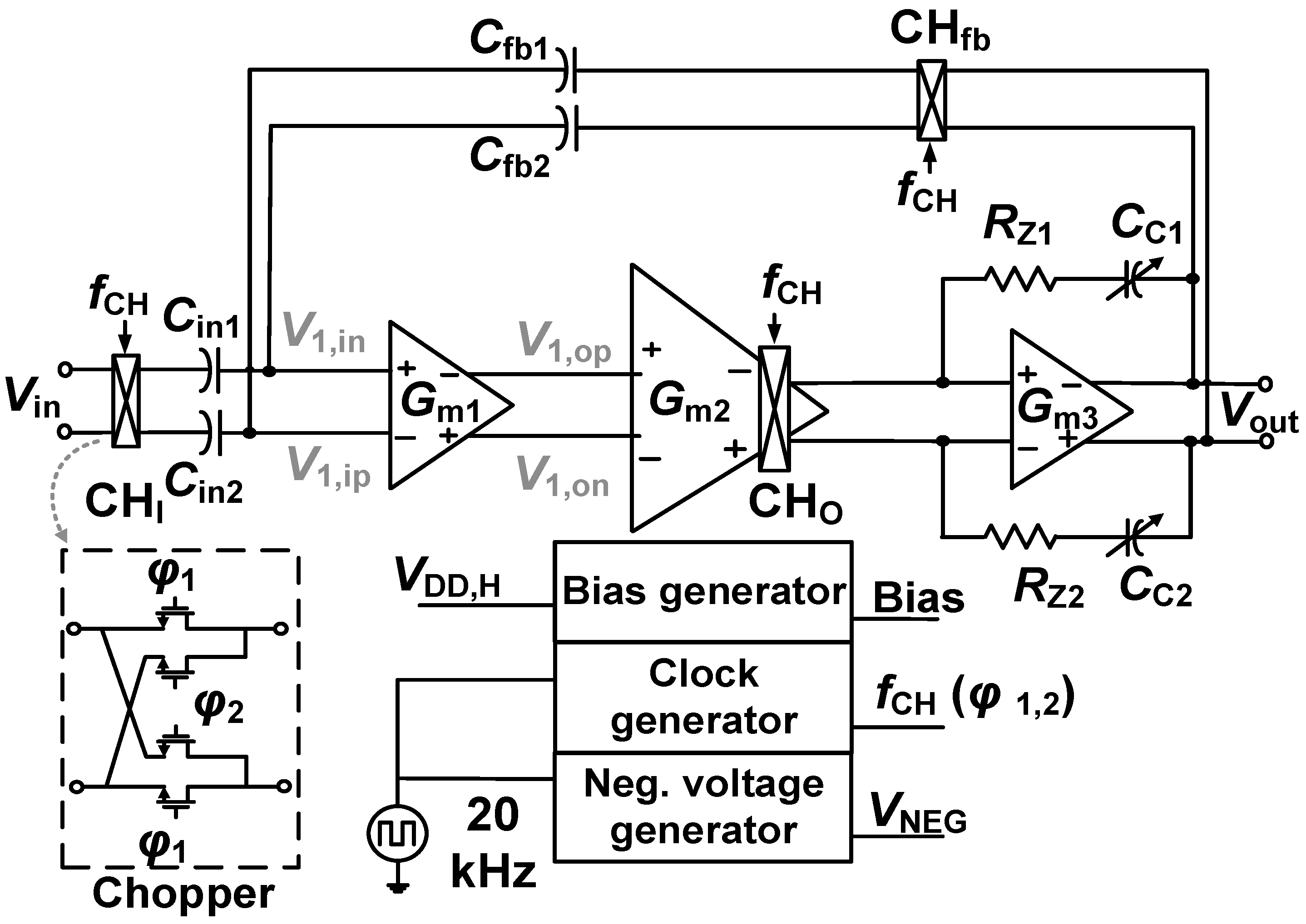
2. Design
3. Circuit Implementation
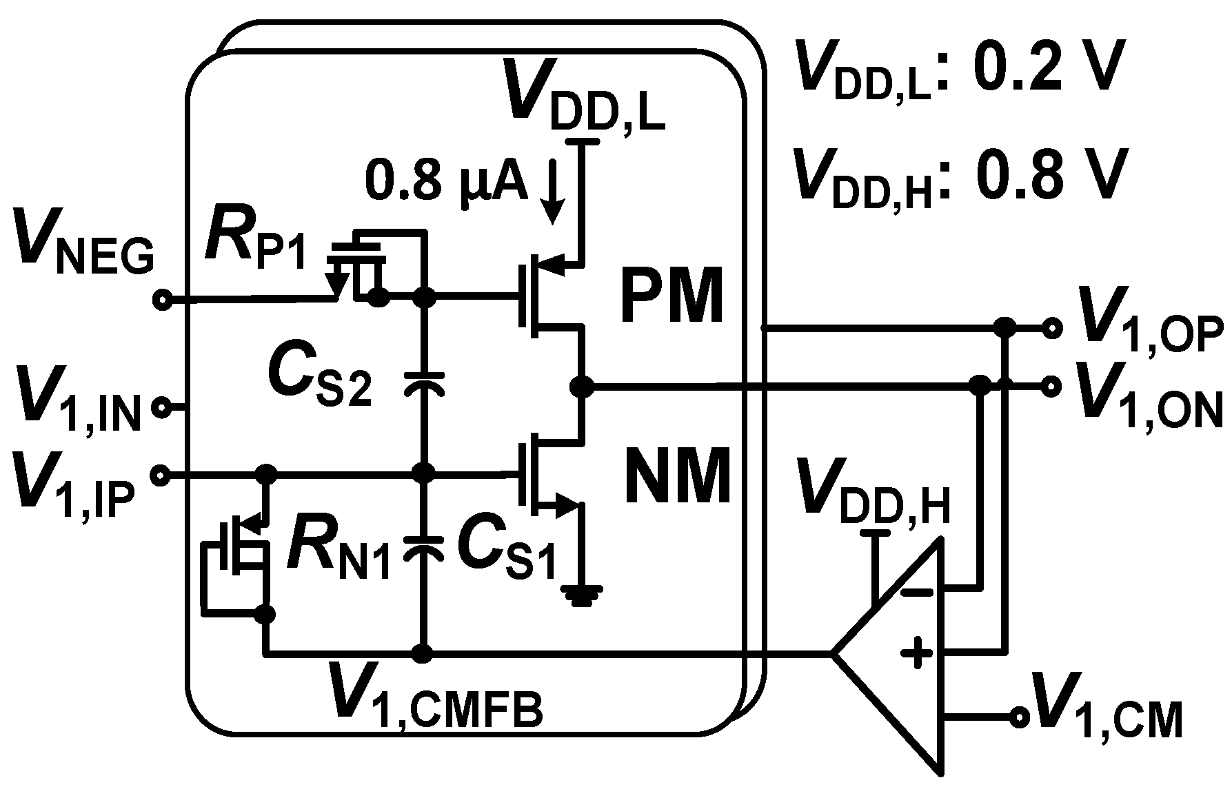
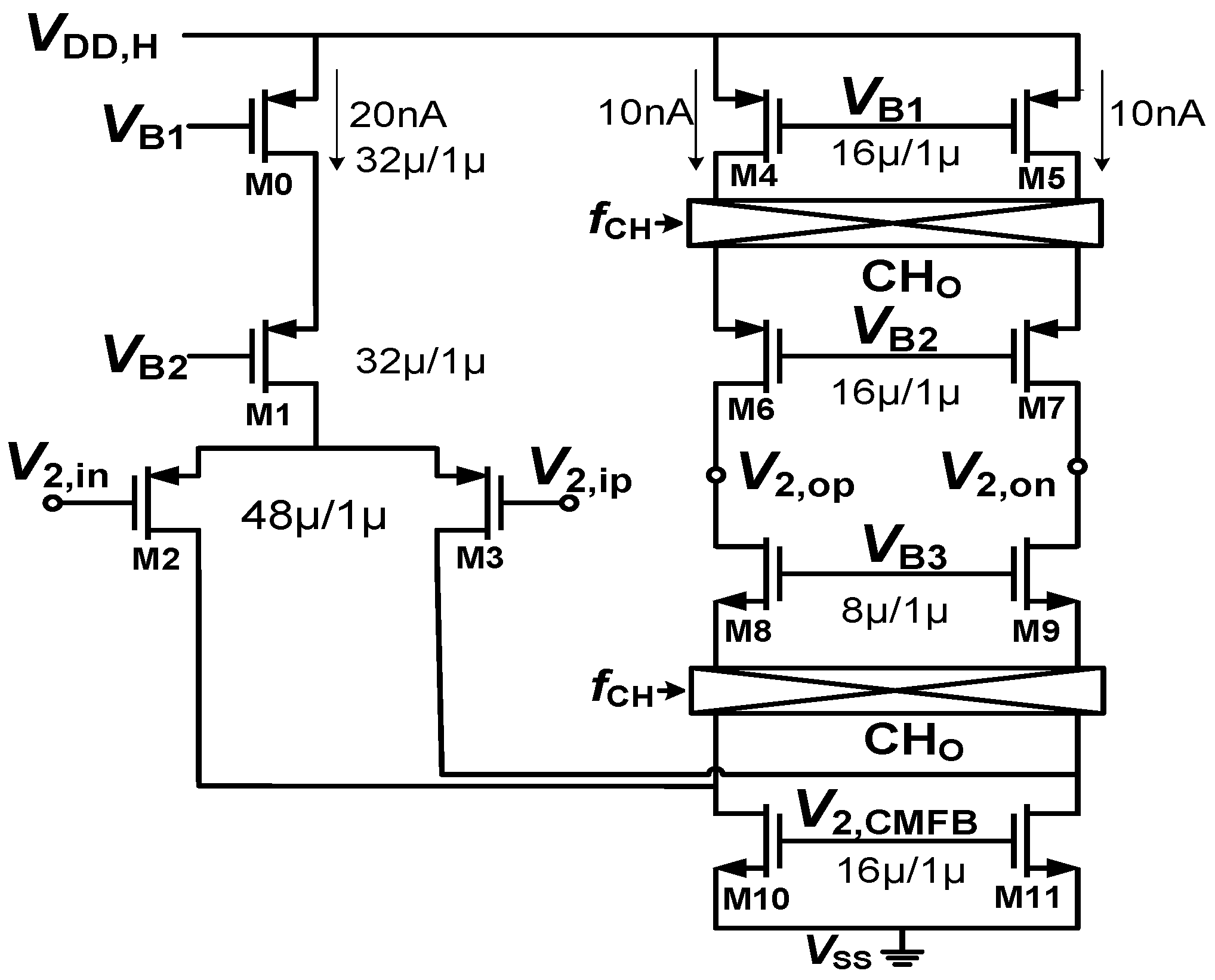
3.1. Squeezed-Inverter Amplifier
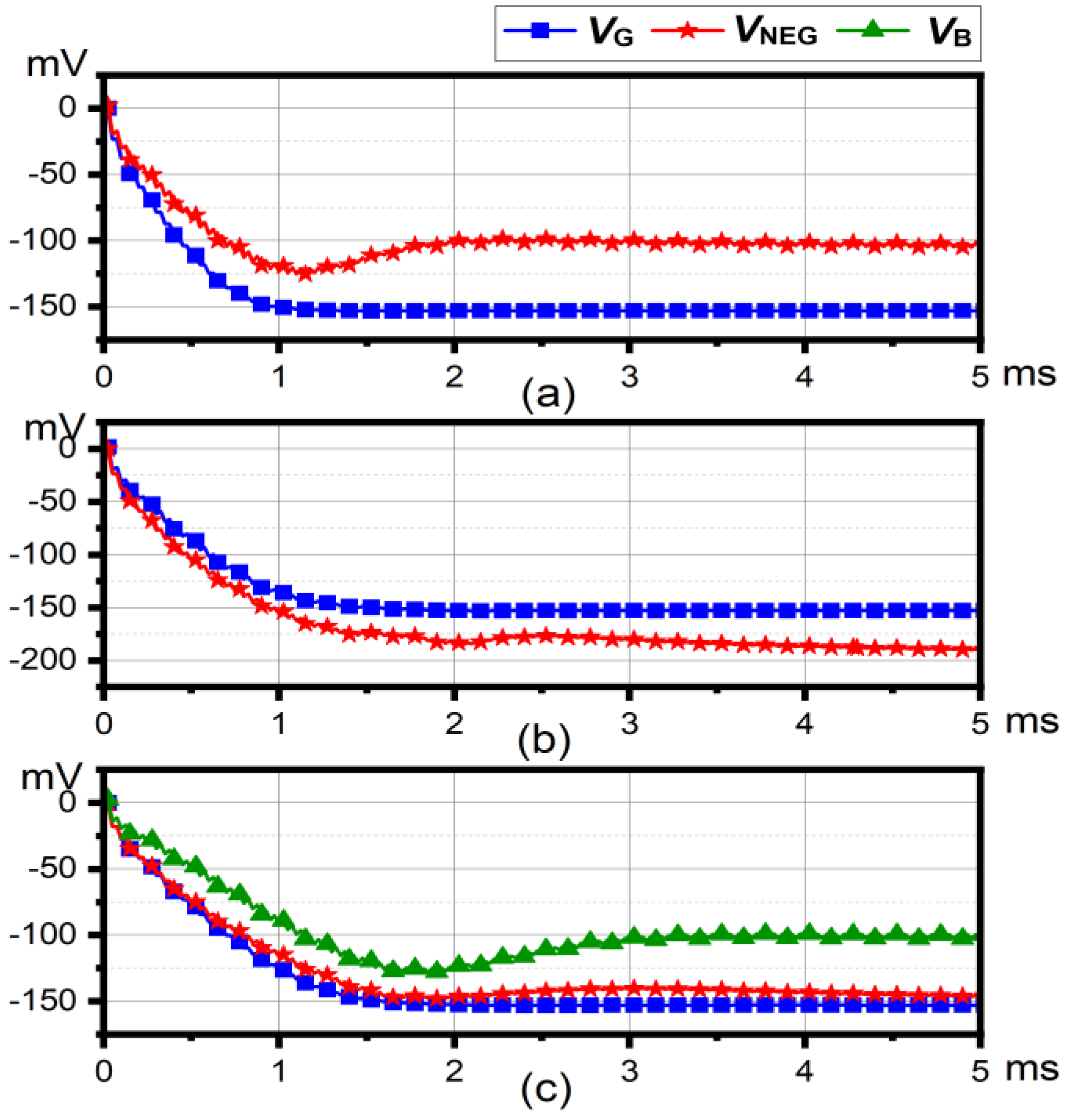
3.2. Bias Circuit for Squeezed-Inverter Amplifier
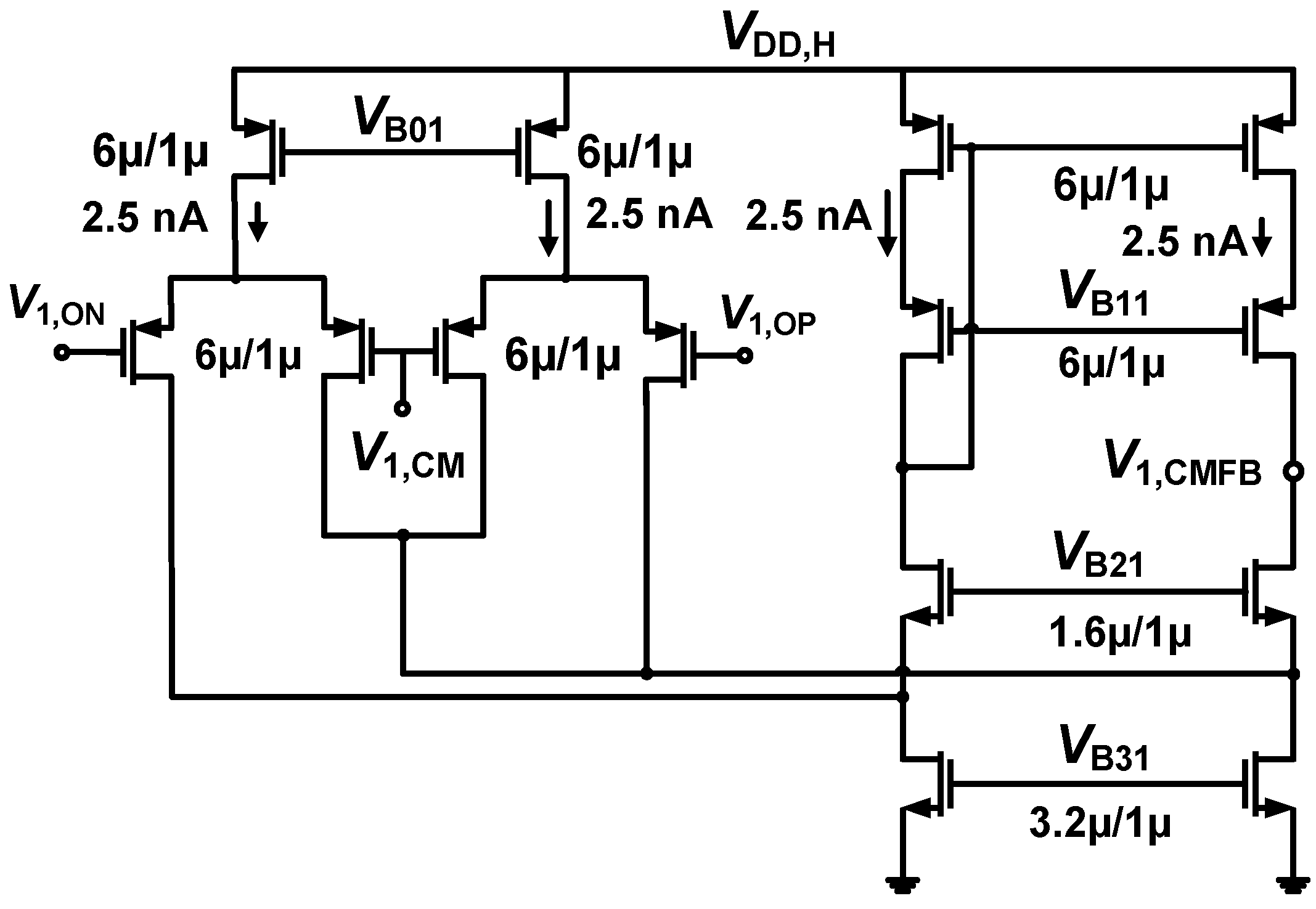
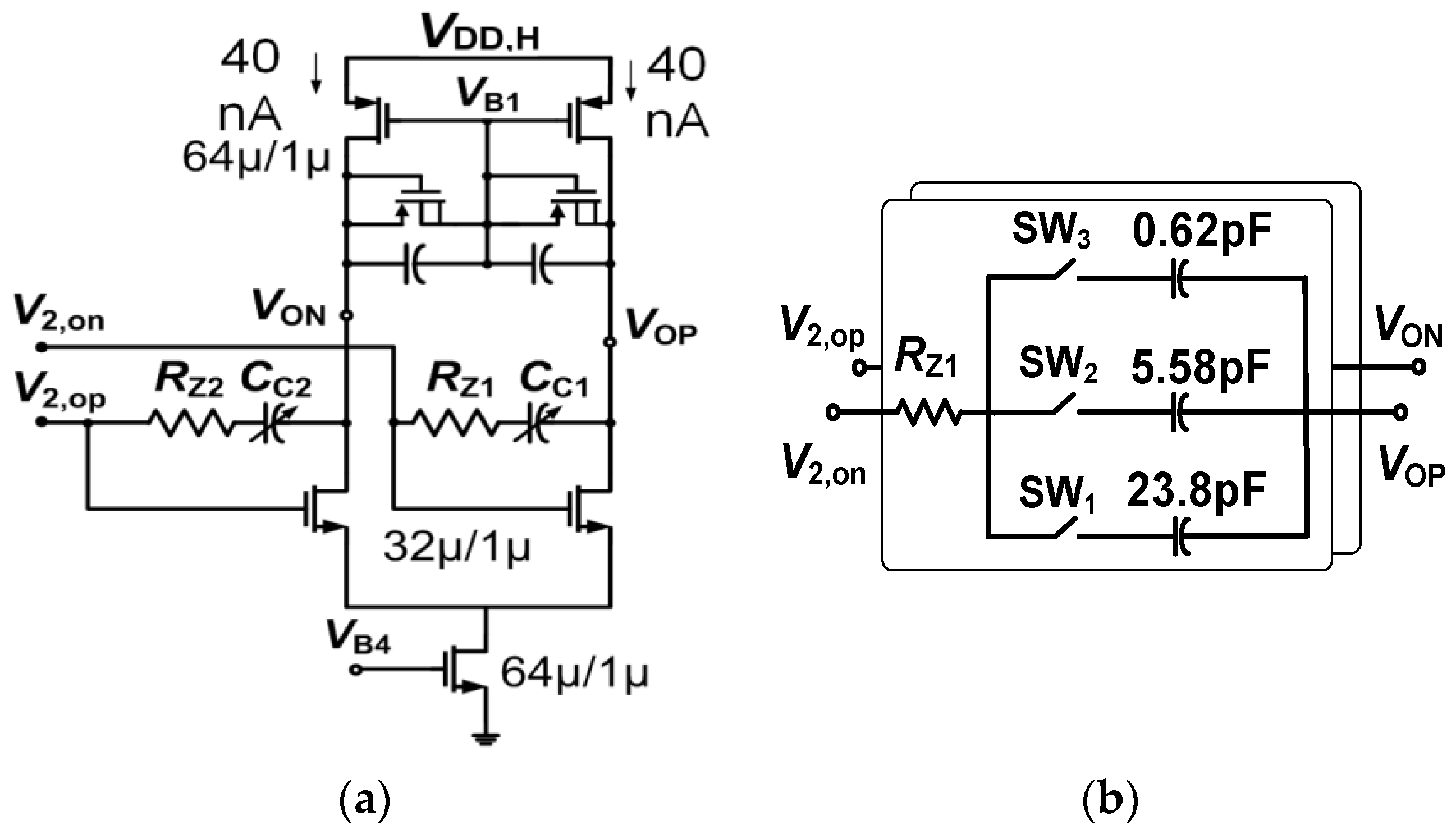
3.3. Middle and Output Stage
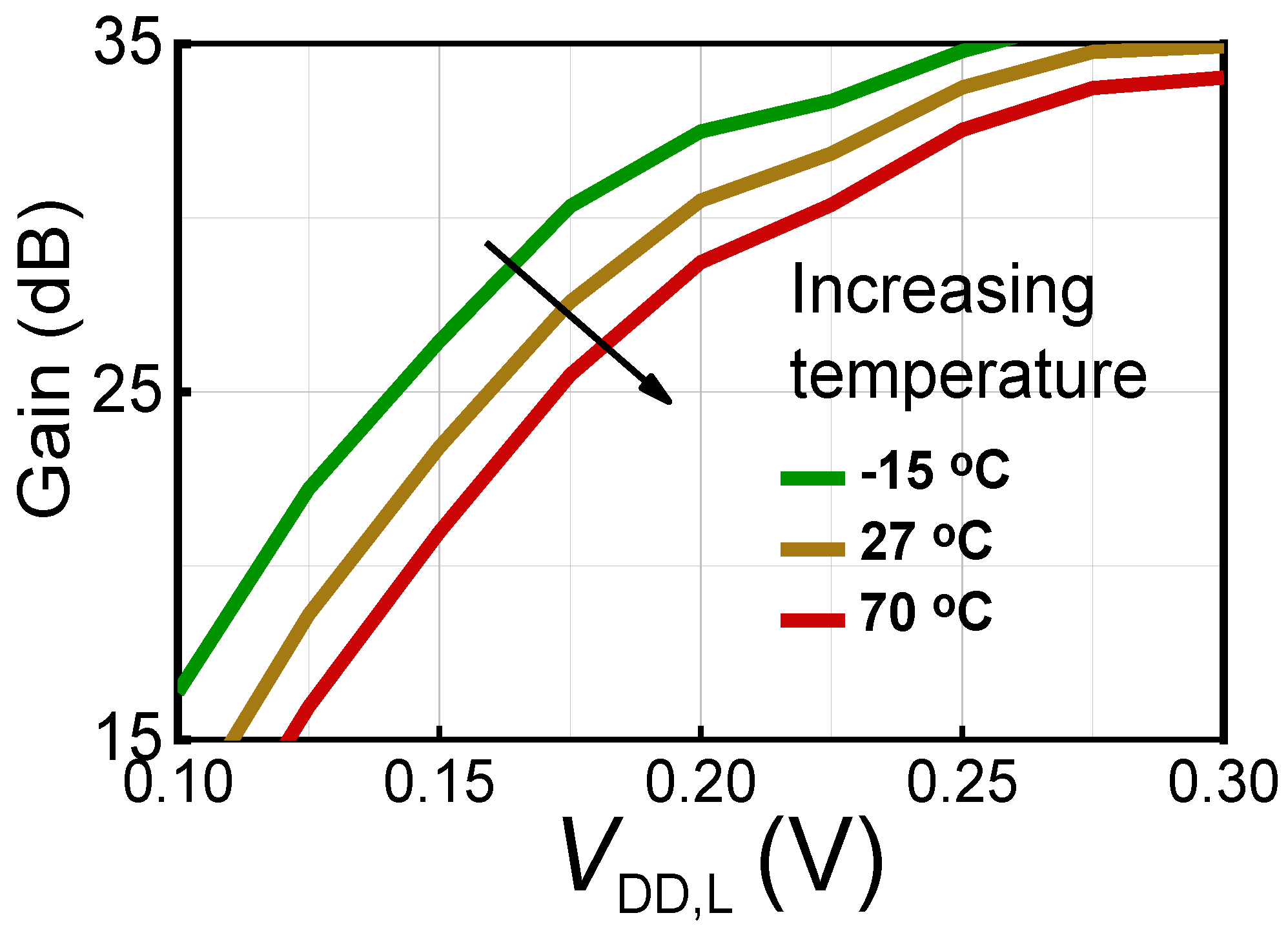
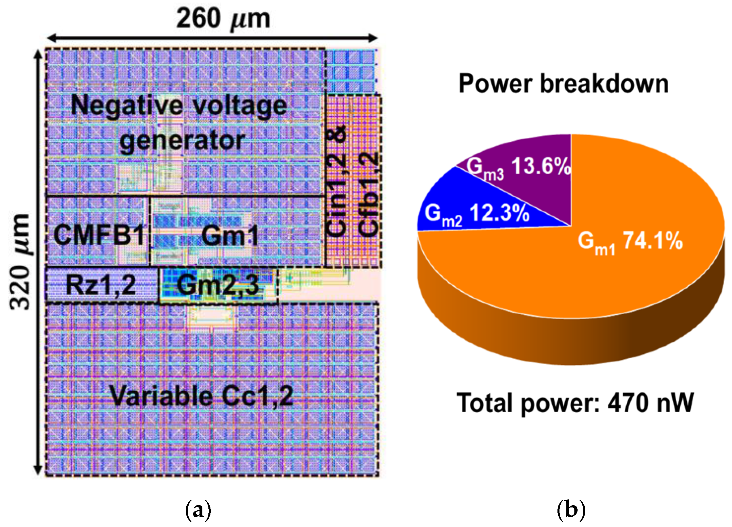
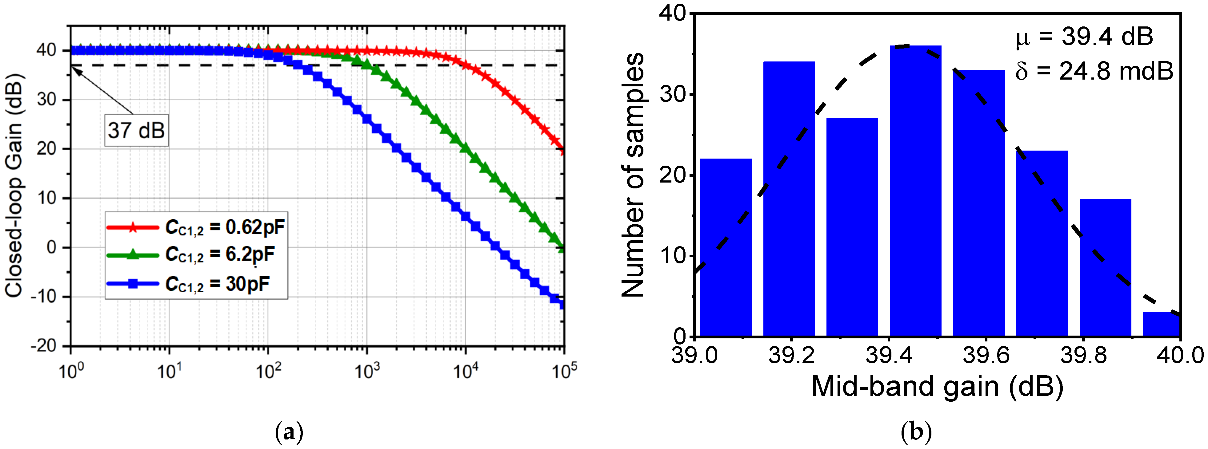
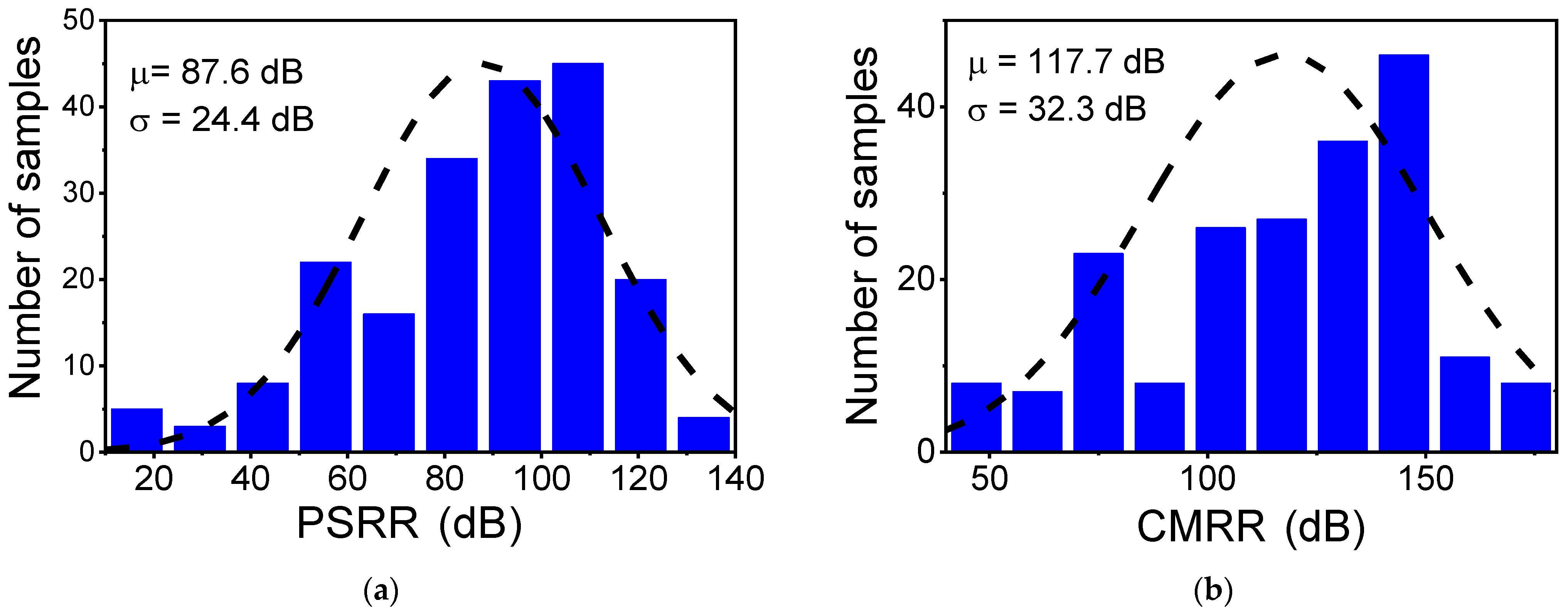
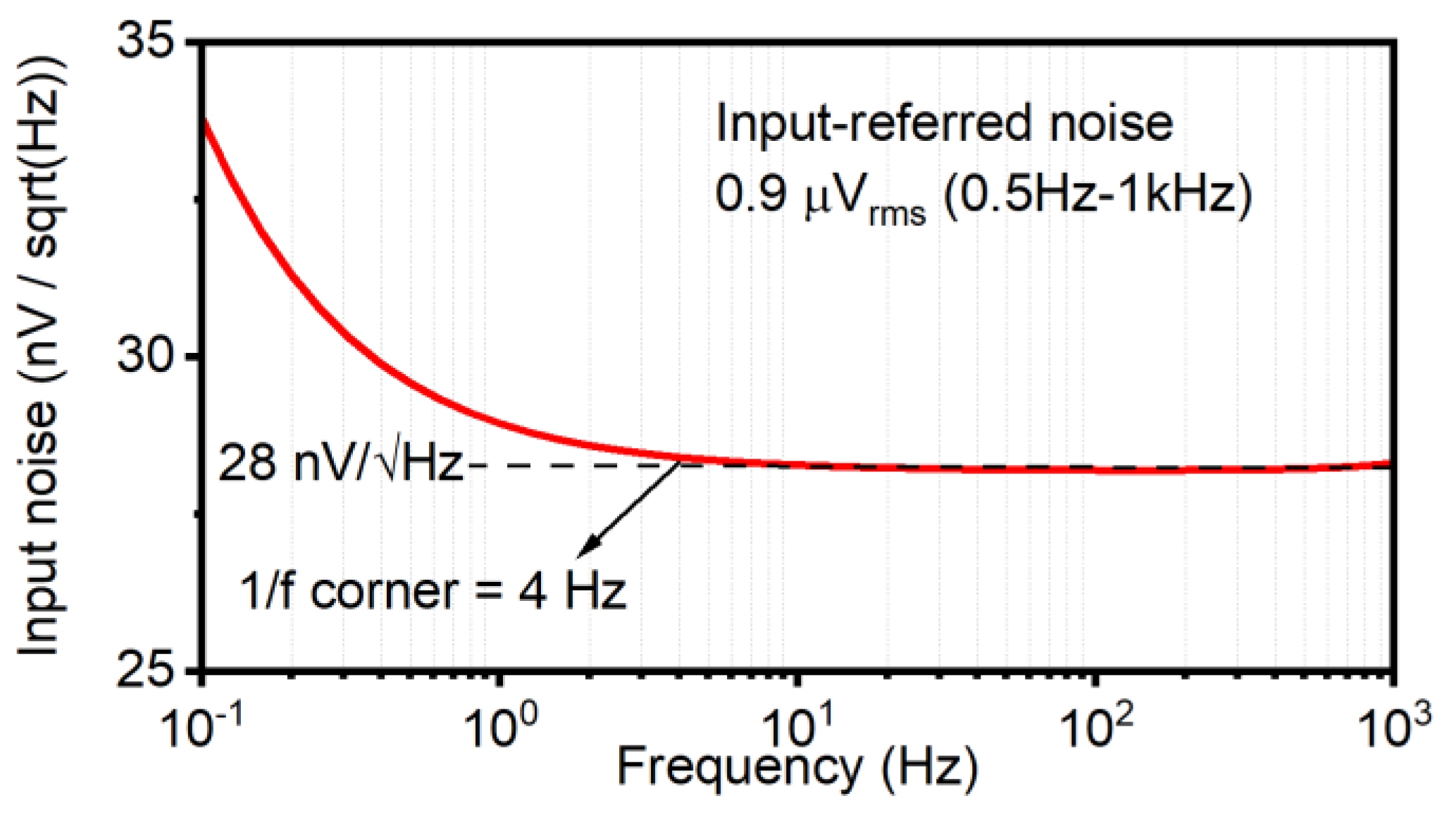
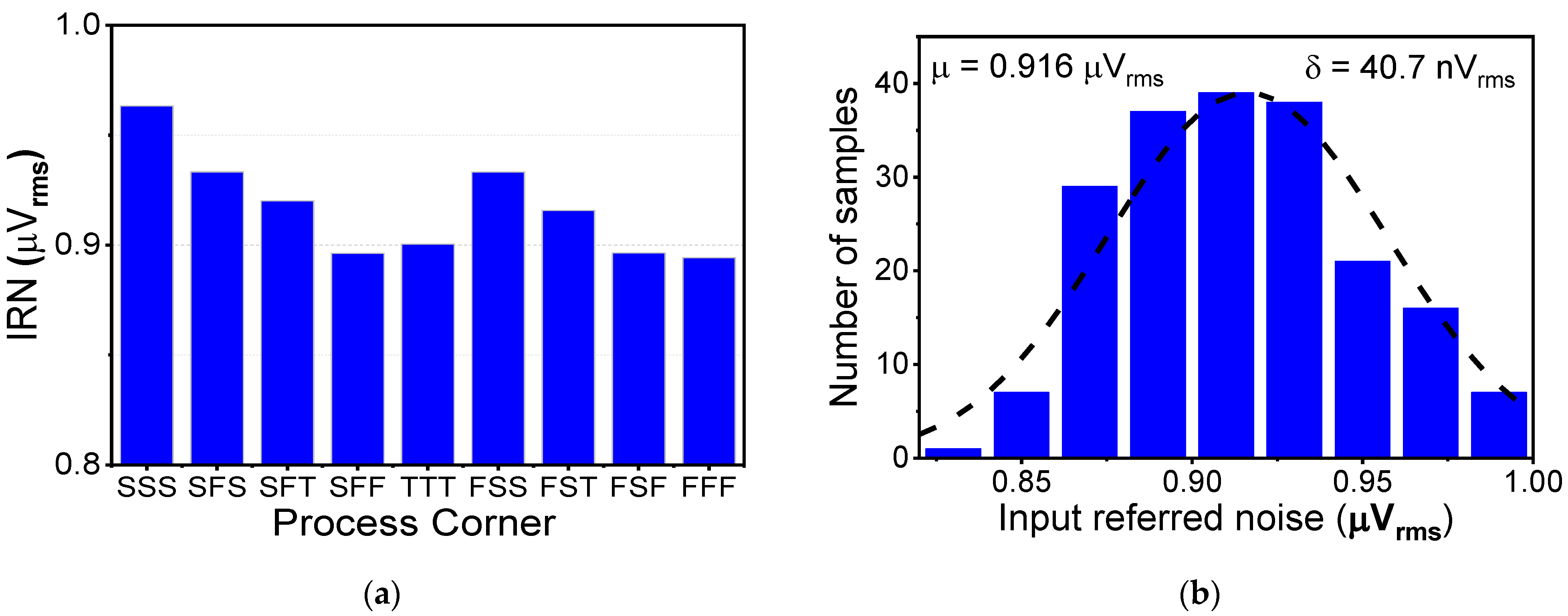
4. Simulation Results
5. Conclusions
Author Contributions
Funding
Conflicts of Interest
References
- Wang, S.; Koickal, T.J.; Hamilton, A.; Mastropaolo, E.; Cheung, R.; Abel, A.; Smith, L.S.; Wang, L. A Power-Efficient Capacitive Read-Out Circuit with Parasitic-Cancellation for MEMS Cochlea Sensors. IEEE Trans. Biomed. Circuits Syst. 2016, 10, 25–37. [Google Scholar] [CrossRef] [PubMed]
- Casson, A.J.; Yates, D.C.; Smith, S.J.M.; Duncan, J.S.; Rodriguez-Villegas, E. Wearable Electroencephalography. IEEE Eng. Med. Biol. Mag. 2010, 29, 44–56. [Google Scholar] [CrossRef] [PubMed]
- Lin, C.T.; Ko, L.W.; Chang, M.H.; Duann, J.R.; Chen, J.Y.; Su, T.P.; Jung, T.P. Review of wireless and wearable electroencephalogram systems and brain-computer interfaces—A mini-review. Gerontology 2010, 56, 112–119. [Google Scholar] [CrossRef] [PubMed]
- Fiedler, P.; Mühle, R.; Griebel, S.; Pedrosa, P.; Fonseca, C.; Vaz, F.; Zanow, F.; Haueisen, J. Contact Pressure and Flexibility of Multipin Dry EEG Electrodes. IEEE Trans. Neural Syst. Rehabil. Eng. 2018, 26, 750–757. [Google Scholar] [CrossRef] [PubMed]
- Chandrakumar, H.; Marković, D. A high dynamic-range neural recording chopper amplifier for simultaneous neural recording and stimulation. IEEE J. Solid-State Circuits 2017, 52, 2811–2828. [Google Scholar] [CrossRef]
- Pham, X.T.; Vu, T.K.; Nguyen, T.D.; Pham, N.L. A 1.2-µW 41-dB Ripple Attenuation Chopper Amplifier Using Auto-Zero Offset Cancelation Loop for Area-Efficient Biopotential Sensing. Electronics 2022, 11, 1149. [Google Scholar] [CrossRef]
- Muller, R.; Gambini, S.; Rabaey, J.M. A 0.013 mm2, 5 μW, DC-Coupled Neural Signal Acquisition IC with 0.5 V Supply. IEEE J. Solid-State Circuits 2012, 47, 232–243. [Google Scholar] [CrossRef]
- Razavi, B. Design of Analog CMOS Integrated Circuits, International ed.; Mc Graw Hill: New York, NY, USA, 2003. [Google Scholar]
- Ha, H.; Hoof, C.V.; Helleputte, N.V. Measurement and Analysis of Input-Signal Dependent Flicker Noise Modulation in Chopper Stabilized Instrumentation Amplifier. IEEE Solid-State Circuits Lett. 2018, 4, 90–93. [Google Scholar] [CrossRef]
- Pham, X.T.; Nguyen, N.T.; Nguyen, V.T.; Lee, J.-W. A 0.6-µW chopper amplifier using a noise-efficient DC servo loop and squeezed-inverter stage for power-efficient biopotential sensing. Sensors 2020, 20, 2059. [Google Scholar] [CrossRef] [PubMed]
- Chandrakumar, H.; Marković, D. An 80-mVpp Linear-Input Range, 1.6-GΩ Input Impedance, Low-Power Chopper Amplifier for Closed-Loop Neural Recording That Is Tolerant to 650-mVpp Common-Mode Interference. IEEE J. Solid-State Circuits 2017, 52, 2811–2828. [Google Scholar] [CrossRef]
- Xu, J.; Lin, Q.; Ding, M.; Li, Y.; Van Hoof, C.; Serdijn, W.; Van Helleputte, N. A 0.6 V 3.8 μW ECG/bio-impedance monitoring IC for disposable health patch in 40 nm CMOS. In Proceedings of the 2018 IEEE Custom Integrated Circuits Conference (CICC), San Diego, CA, USA, 8–11 April 2018. [Google Scholar]
- Muller, R.; Le, H.P.; Li, W.; Ledochowitsch, P.; Gambini, S.; Bjorninen, T.; Koralek, A.; Carmena, J.M.; Maharbiz, M.M.; Alon, E.; et al. A Minimally Invasive 64-Channel Wireless μECoG Implant. IEEE J. Solid-State Circuits 2015, 50, 344–359. [Google Scholar] [CrossRef]
- Park, J.H.; Tang, T.; Zhang, L.; Ng, K.A.; Gammad, G.G.L.; Yen, S.C.; Yoo, J. A 15-Channel Orthogonal Code Chopping Instrumentation Amplifier for Area-Efficient, Low-Mismatch Bio-Signal Acquisition. IEEE J. Solid-State Circuits 2020, 55, 2771–2780. [Google Scholar] [CrossRef]
- Nguyen, T.V.; Han, H.-D.; Pham, N.L.; Pham, X.T.; Hoang, M.K. A 0.47-μW Multi-stage Low Noise Amplifier Employing 0.2-V-supply OTA. In Proceedings of the 2022 IEEE Ninth International Conference on Communications and Electronics (ICCE), Nha Trang, Vietnam, 27–29 July 2022. [Google Scholar]
- Yaul, F.M.; Chandrakasan, A.P. A noise-efficient 36 nV/√Hz chopper amplifier using an inverter-based 0.2-V supply input stage. IEEE J. Solid-State Circuits 2017, 52, 3032–3042. [Google Scholar] [CrossRef]
- Pham, X.T.; Nguyen, V.-N.; Kim, J.-S.; Lee, J.-W. A 0.52 μW, 38 nV/√Hz chopper amplifier with a low-noise DC servo loop, an embedded ripple reduction loop, and a squeezed inverter stage. IEEE Trans Circuits Syst. II Express Briefs 2021, 68, 1793–1797. [Google Scholar] [CrossRef]
- Huang, G.; Yin, T.; Wu, Q.; Zhu, Y.; Yang, H. A 1.3 μW 0.7 μVRMS chopper current-reuse instrumentation amplifier for EEG applications. In Proceedings of the 2015 IEEE International Symposium on Circuits and Systems (ISCAS), Lisbon, Portugal, 24–27 May 2015. [Google Scholar]
- Liu, Y.; Zhou, Z.; Zhou, Y.; Li, W.; Wang, Z. A Low-Noise Chopper Amplifier with Offset and Low-Frequency Noise Compensation DC Servo Loop. Electronics 2020, 9, 1797. [Google Scholar] [CrossRef]
- Omidvar, A.; Shaterian, M. A low-power digitally programmable neural recording amplifier with selectable multiunit activity (MUA) and local field potential (LFP) recording modes. Microelectron. J. 2020, 95, 104654. [Google Scholar] [CrossRef]
- Nasseriana, M.; Peiravia, A.; Moradi, F. A fully-integrated 16-channel EEG readout front-end for neural recording applications. AEU—Int. J. Electron. Commun. 2018, 94, 109–121. [Google Scholar]
- Fang, L.; Gui, P. A Low-Noise Low-Power Chopper Instrumentation Amplifier with Robust Technique for Mitigating Chopping Ripples. IEEE J. Solid-State Circuits 2022, 57, 1800–1811. [Google Scholar] [CrossRef]
- Del Cesta, S.; Ria, A.; Piotto, M.; Simmarano, R.; Bruschi, P. A compact current-mode instrumentation amplifier for general-purpose sensor interfaces. AEU—Int. J. Electron. Commun. 2018, 92, 8–14. [Google Scholar]


| Miller Compensate Capacitors CC1,2 (pF) | 30 | 6.2 | 0.62 |
|---|---|---|---|
| Bandwidth—BW (kHz) | 0.2 | 1 | 10 |
| Thermal noise (nV/√H z) | 28 | 28 | 28 |
| Input-referred noise—Vni,rms (µVrms) | 0.4 | 0.9 | 2.8 |
| Noise Efficiency Factor () | 1.49 | 1.49 | 1.47 |
| Power Efficiency Factor () | 0.56 | 0.56 | 0.55 |
| Ref. | [6] | [16] | [17] | [19] | [20] | [21] | [22] | [23] | This Work |
|---|---|---|---|---|---|---|---|---|---|
| Year | 2022 | 2017 | 2021 | 2020 | 2020 | 2018 | 2022 | 2018 | 2023 |
| Supply (V) | 1 | 0.2/0.8 | 0.2/0.8 | 1.8 | 1.2 | 1 | 0.5/1.8 | 1.5/3.3 | 0.2/0.8 |
| Power (µW) | 1.21 | 0.79 | 0.52 | 3.96 | 1.9 | 0.96 | 4.5 | 330 | 0.47 |
| Gain (dB) | 40 | 57.8 | 39.6 | 31.7 | 58.4 | 62 | 60 | 1/12/20/40 | 40 |
| Bandwidth (kHz) | 0.8 | 0.67 | 0.8 | 9 | 8.7 | 0.23 | 300 | 1250 | 0.2/1/10 |
| Flexible Bandwidth | N | N | N | N | Y | N | N | N | Y |
| Thermal noise (nV/√Hz) | 121 | 36 | 32 | 49.5 | N/A | N/A | 13 | 60 | 28 |
| CMRR (dB) | 108 | 85 | 104 | 85 | 110 | 88 | 84 | 90 | 117.7 |
| PSRR (dB) | 87 | 80 | 82 | 87 | 87 | 101 | 88 | 100 | 87.6 |
| 5.4 | 2.1 | 1.7 | 2.08 | 1.47 | 3.34 | 1.3 | 29 | 1.49 | |
| 29.7 | 1.6 | 0.7 | 7.78 | 2.59 | 9.06 | 1.1 | N/A | 0.56 | |
| Tech. (nm) | 180 | 180 | 180 | 180 | 130 | 180 | 180 | 180 | 180 |
| Sim./Meas. | Sim. | Meas. | Meas. | Sim. | Sim. | Sim. | Meas. | Meas. | Sim. |
Disclaimer/Publisher’s Note: The statements, opinions and data contained in all publications are solely those of the individual author(s) and contributor(s) and not of MDPI and/or the editor(s). MDPI and/or the editor(s) disclaim responsibility for any injury to people or property resulting from any ideas, methods, instructions or products referred to in the content. |
© 2023 by the authors. Licensee MDPI, Basel, Switzerland. This article is an open access article distributed under the terms and conditions of the Creative Commons Attribution (CC BY) license (https://creativecommons.org/licenses/by/4.0/).
Share and Cite
Pham, X.T.; Kieu, X.T.; Hoang, M.K. Ultra-Low Power Programmable Bandwidth Capacitively-Coupled Chopper Instrumentation Amplifier Using 0.2 V Supply for Biomedical Applications. J. Low Power Electron. Appl. 2023, 13, 37. https://doi.org/10.3390/jlpea13020037
Pham XT, Kieu XT, Hoang MK. Ultra-Low Power Programmable Bandwidth Capacitively-Coupled Chopper Instrumentation Amplifier Using 0.2 V Supply for Biomedical Applications. Journal of Low Power Electronics and Applications. 2023; 13(2):37. https://doi.org/10.3390/jlpea13020037
Chicago/Turabian StylePham, Xuan Thanh, Xuan Thuc Kieu, and Manh Kha Hoang. 2023. "Ultra-Low Power Programmable Bandwidth Capacitively-Coupled Chopper Instrumentation Amplifier Using 0.2 V Supply for Biomedical Applications" Journal of Low Power Electronics and Applications 13, no. 2: 37. https://doi.org/10.3390/jlpea13020037