
Design and Optimization of an Ultra-Low-Power Cross-Coupled LC VCO with a DFF Frequency Divider for 2.4 GHz RF Receivers Using 65 nm CMOS Technology


Abstract
:1. Introduction
1.1. Quadrature Generation VCO
1.2. The Contribution
2. Literature Review
Commonly Used Techniques in Traditional Low-Voltage LC-VCO
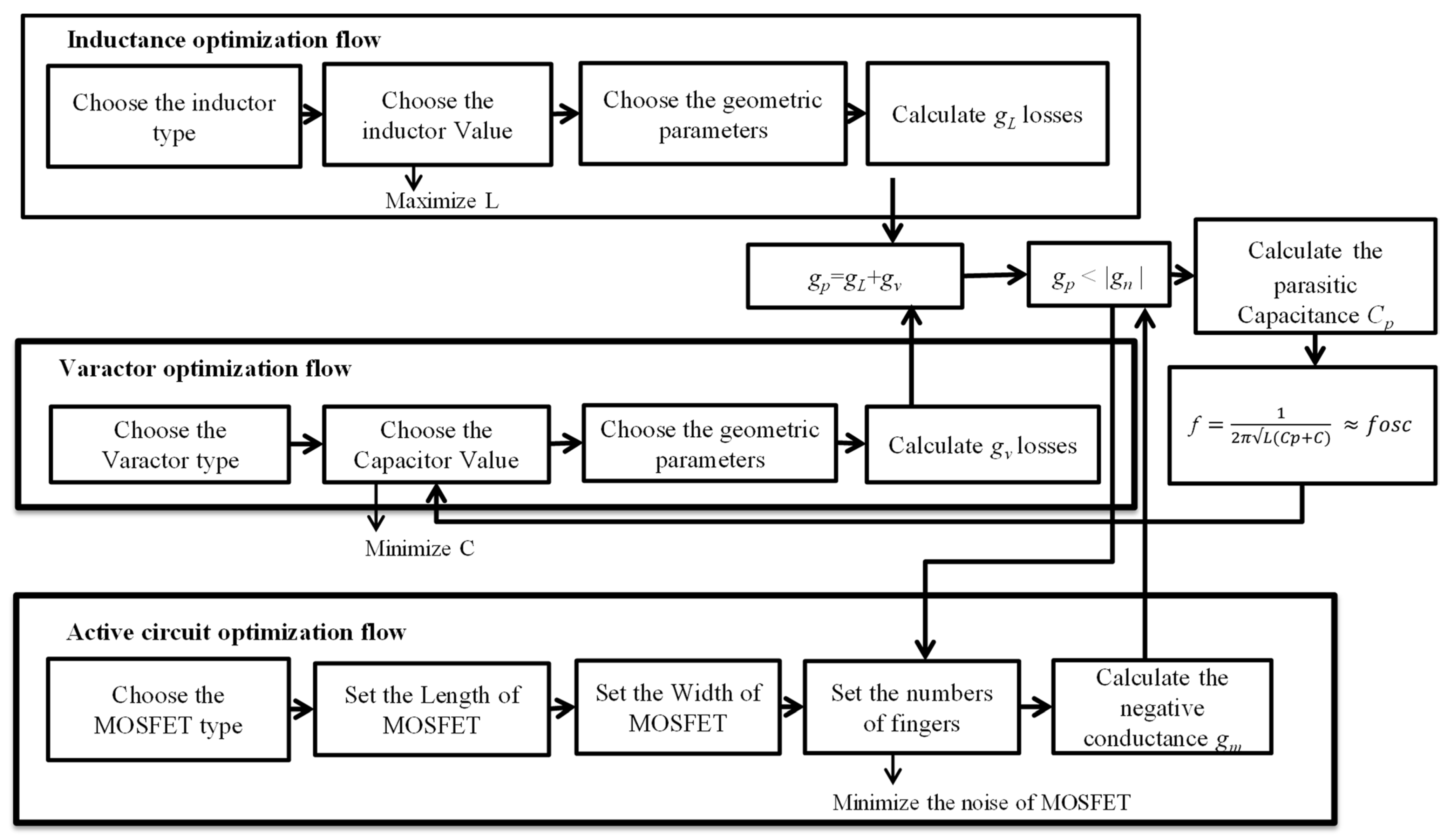
3. Design Methodology
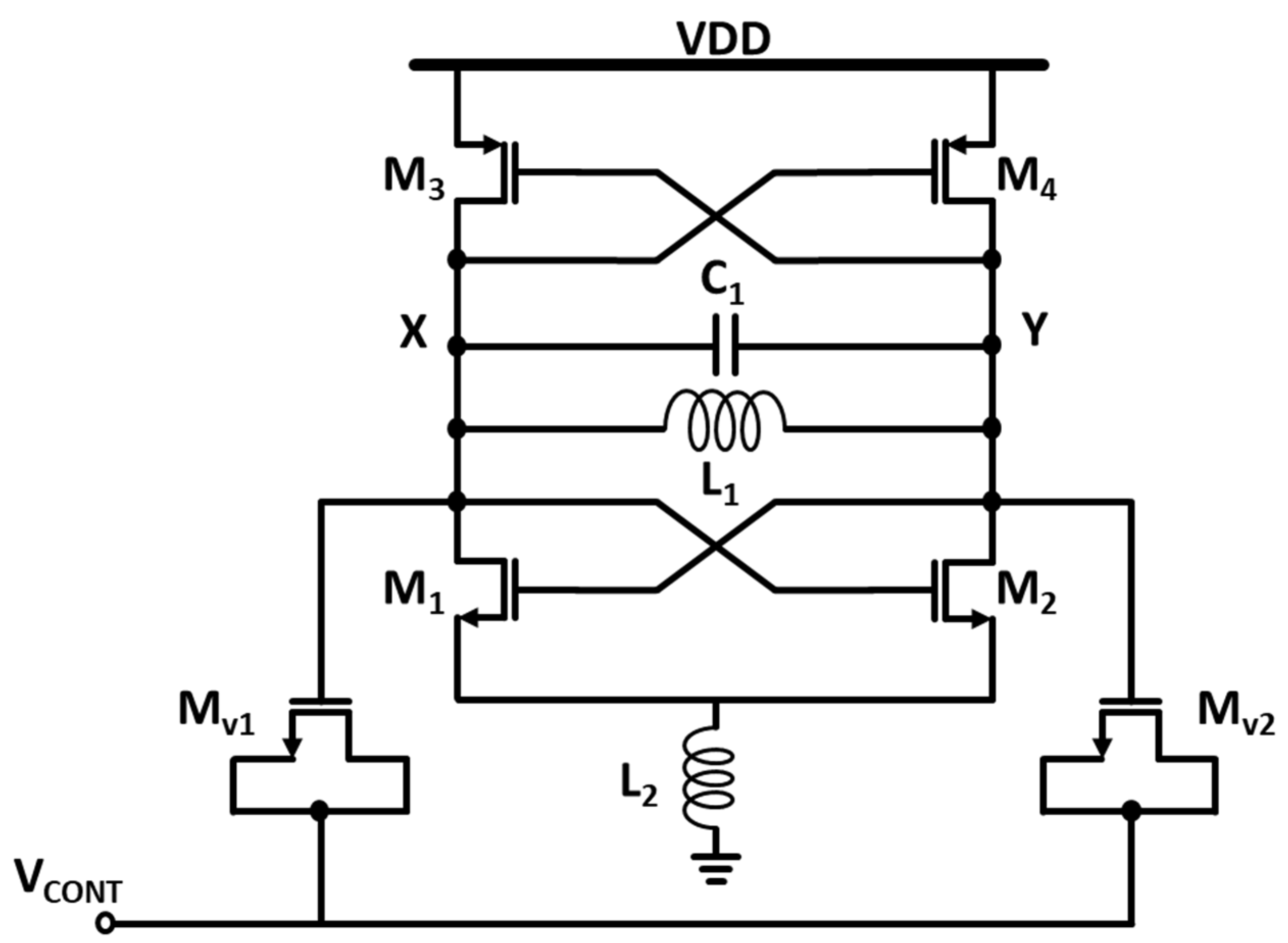
3.1. The Proposed Circuit Design
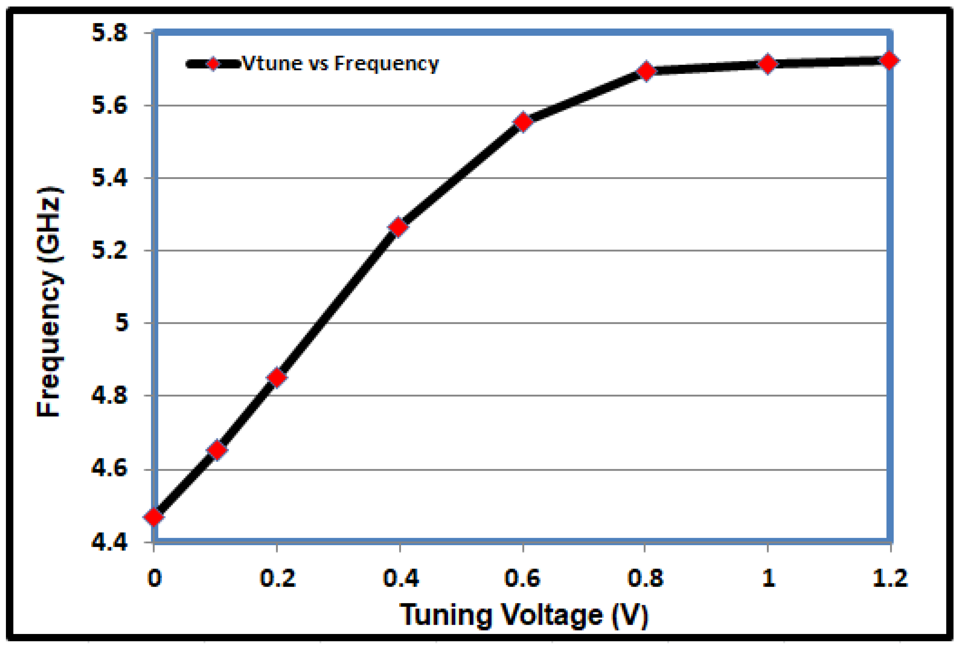
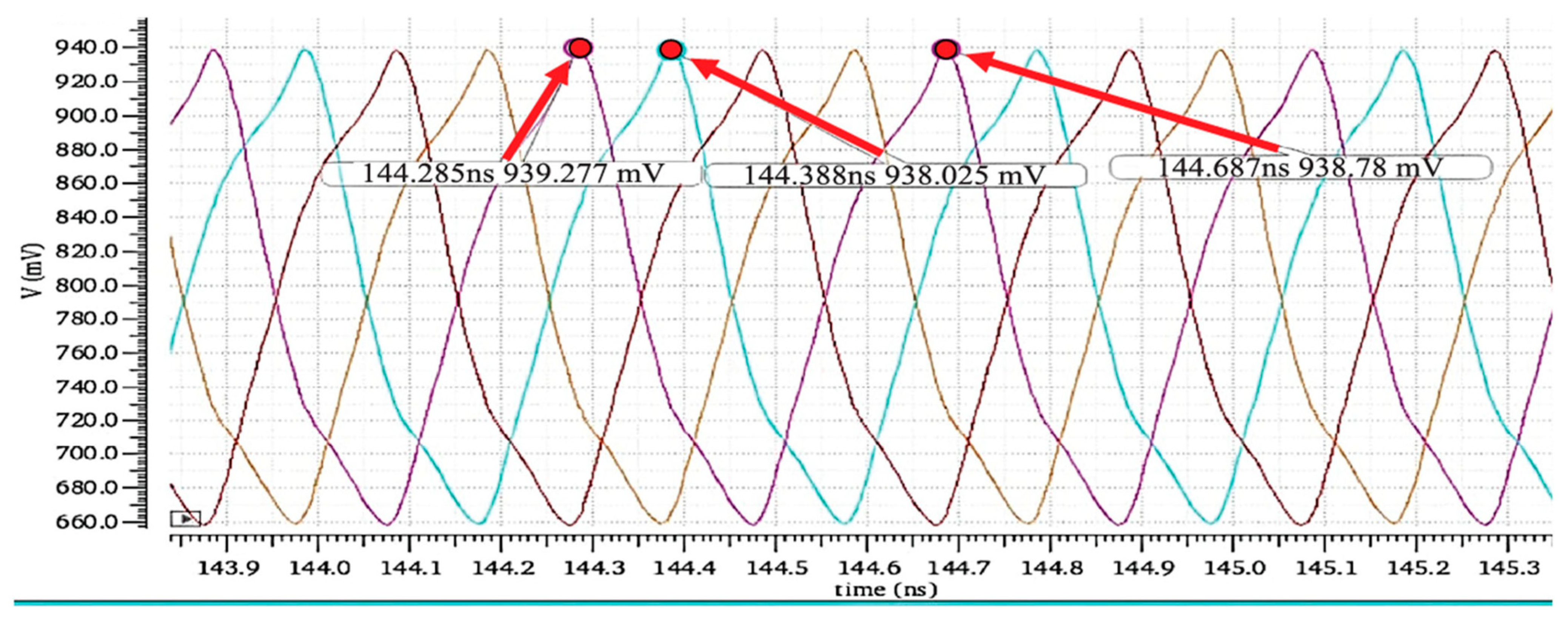
3.2. A Quadrature Differential Cross-Coupled LC VCO Is Proposed
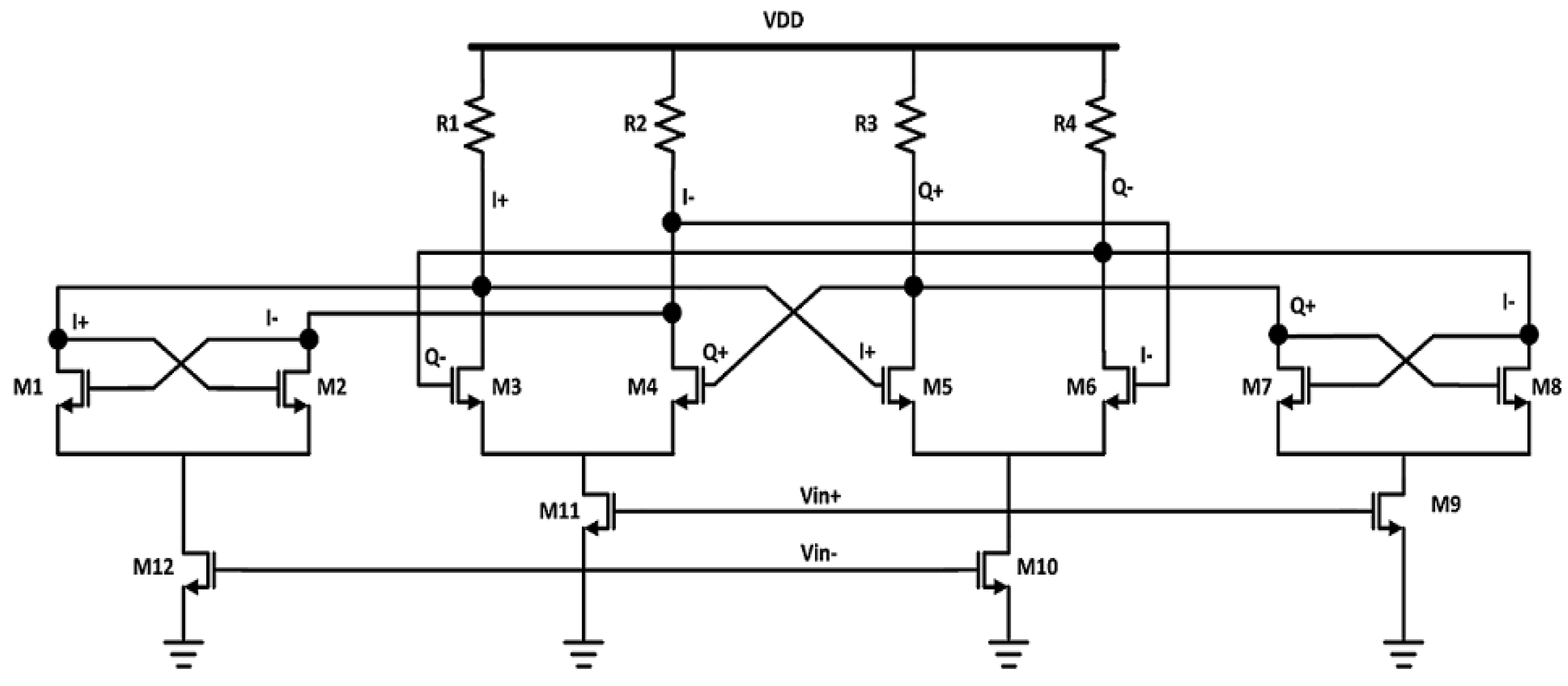
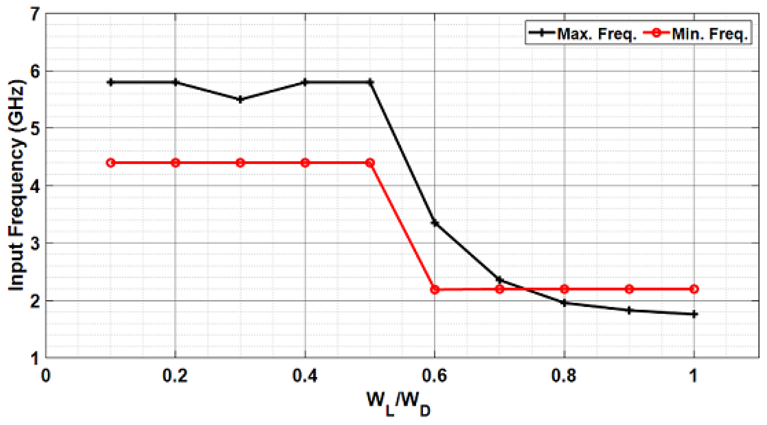
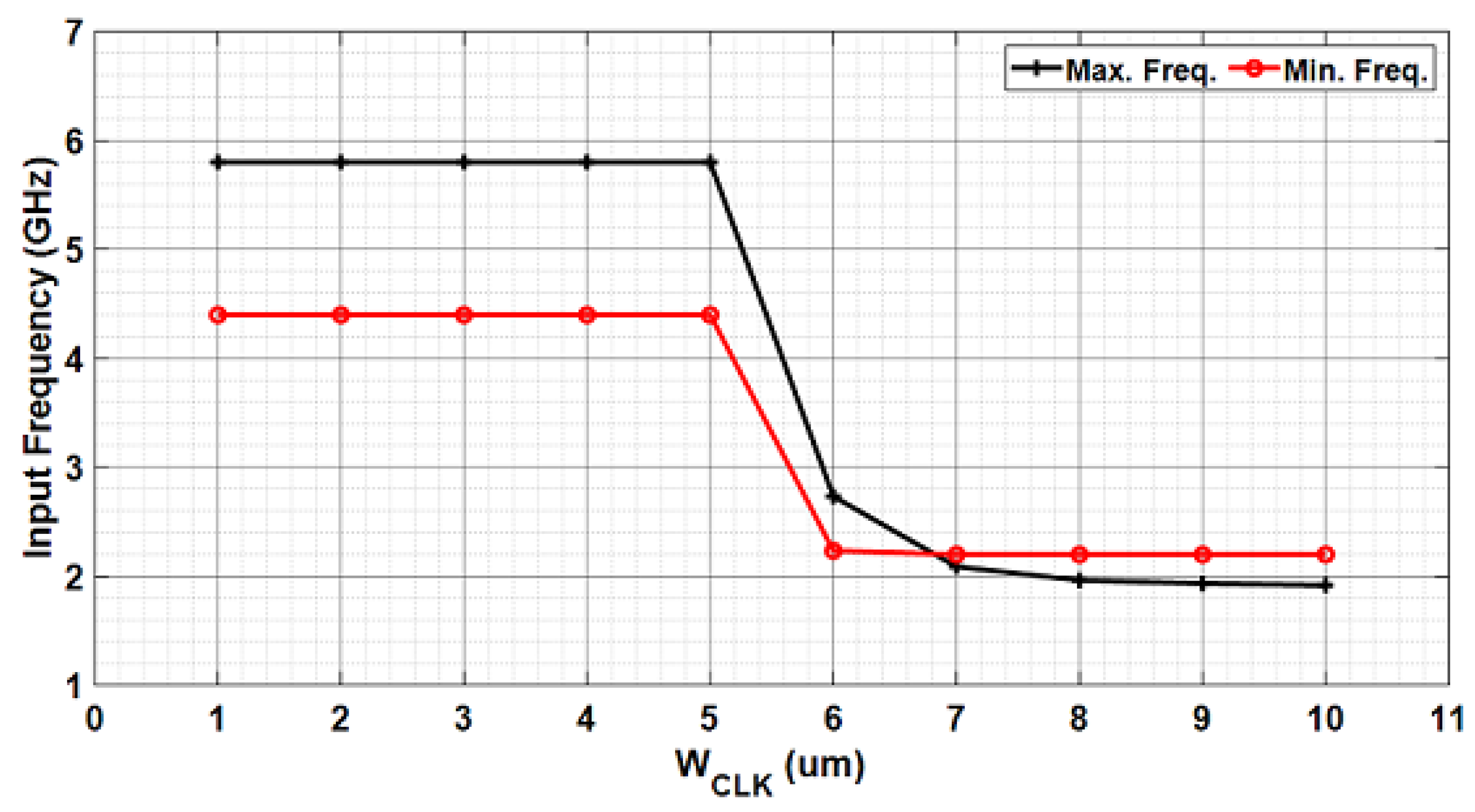
3.3. Frequency Divider Design
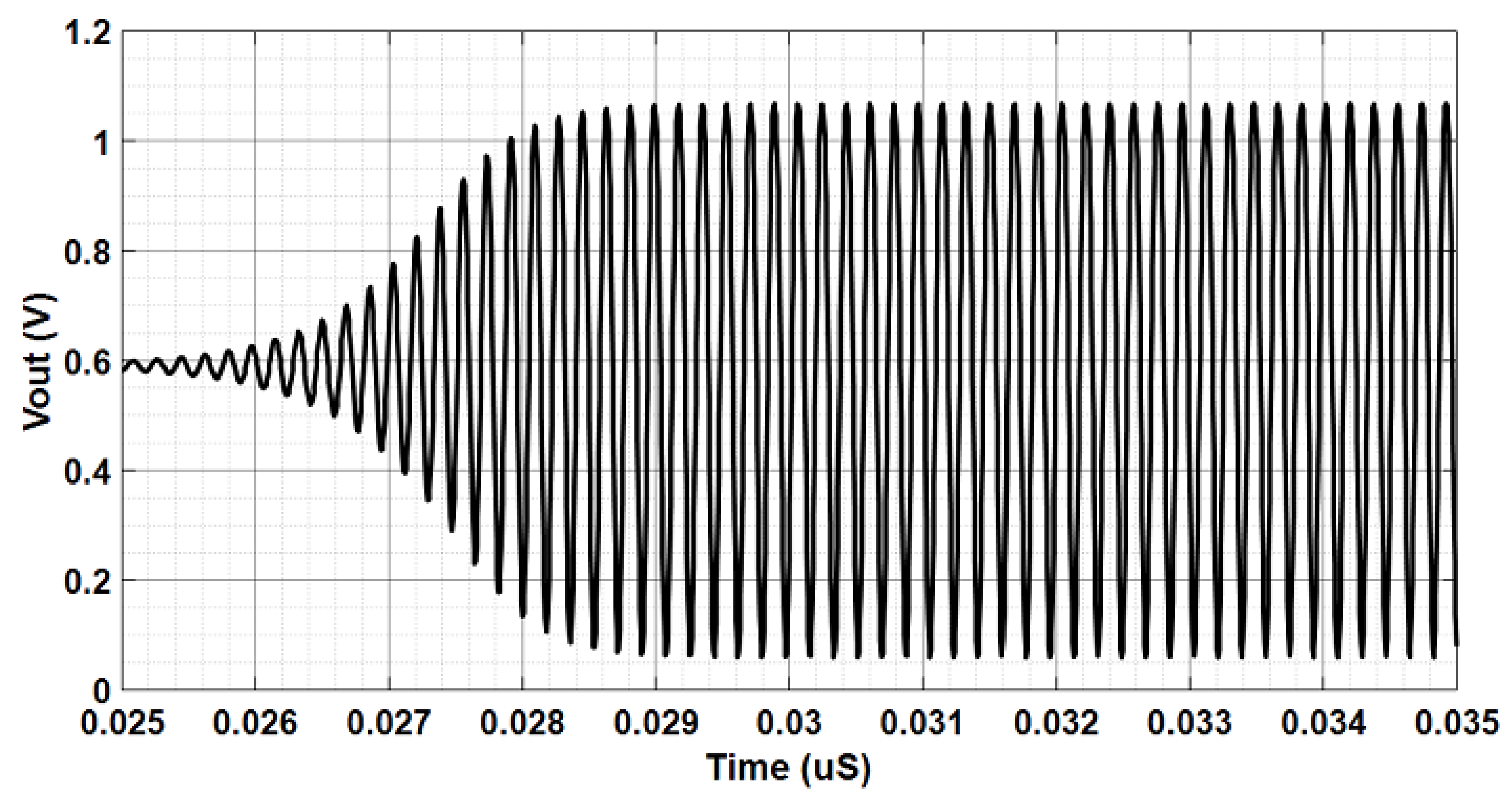
4. Post-Layout Simulation Results Using the TSMC 65 nm CMOS Process
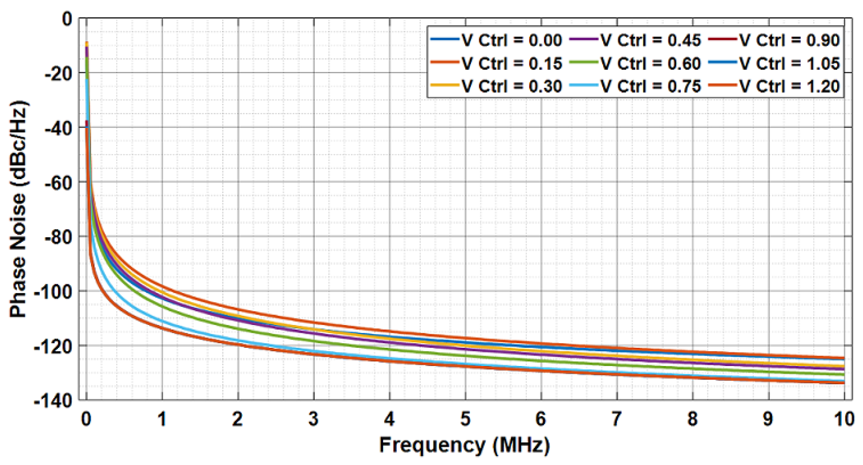
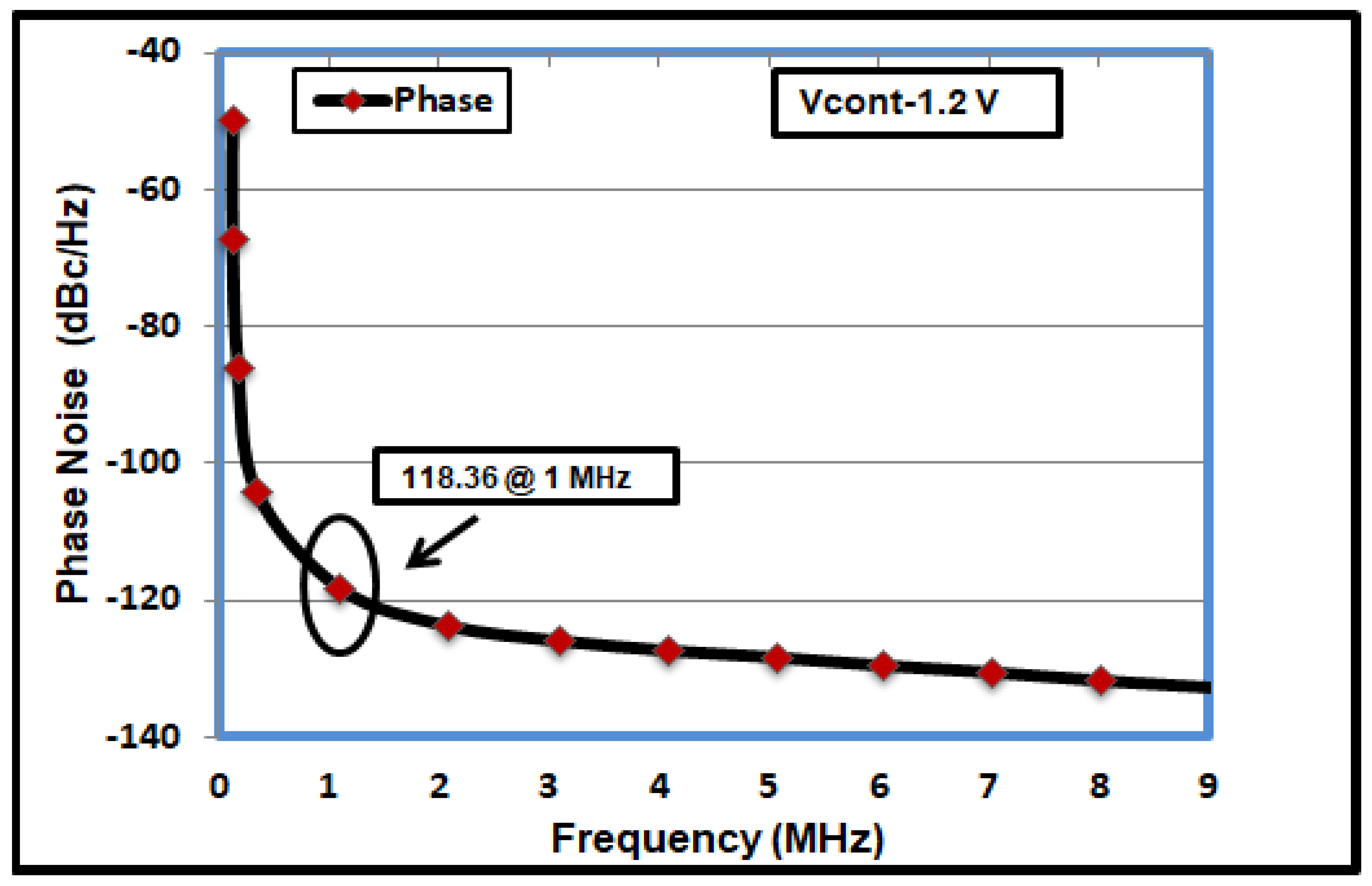
4.1. Phase Noise
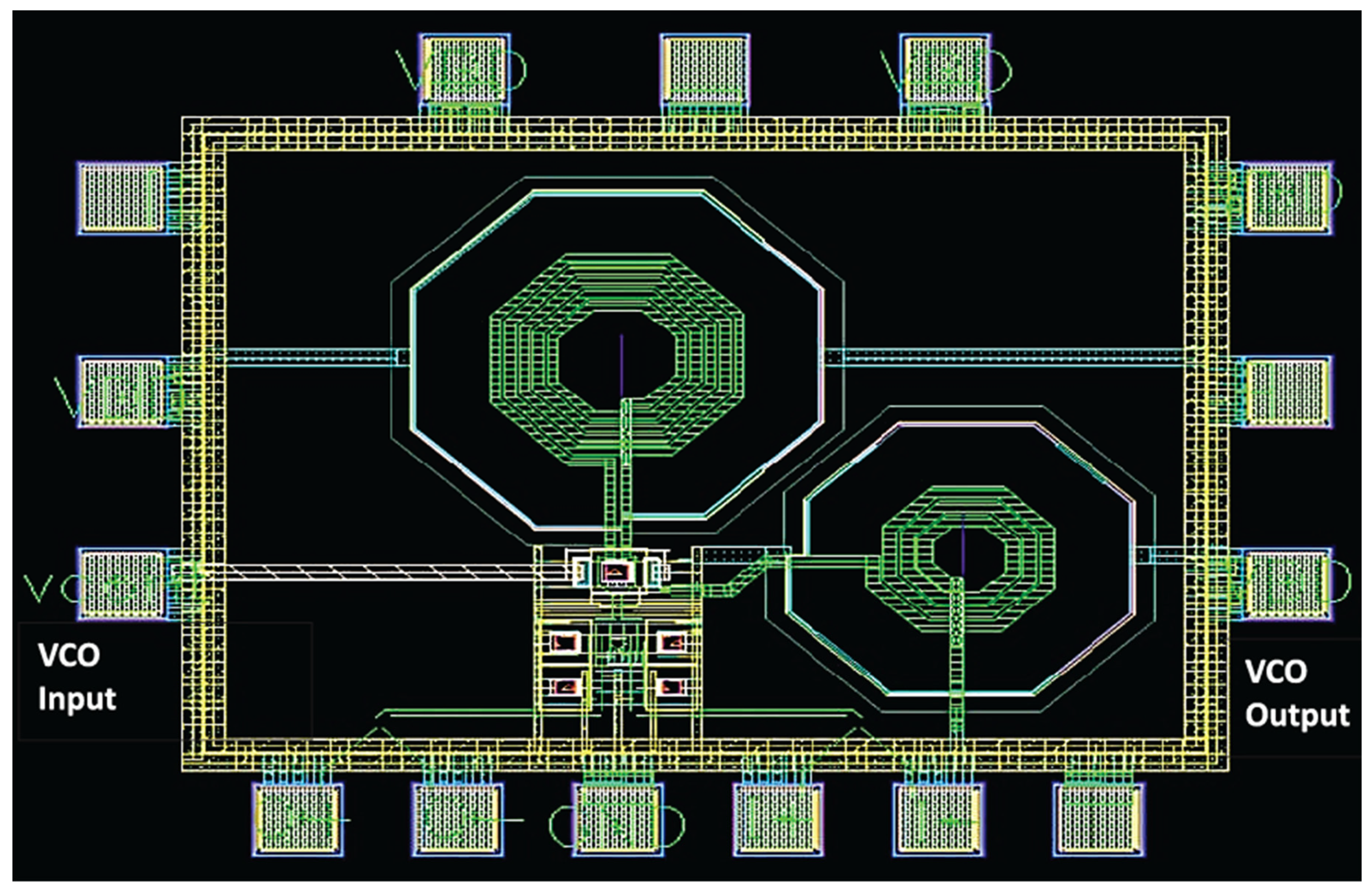
4.2. Design Layout
4.3. Comparison with Previous Work
5. Conclusions
Author Contributions
Funding
Data Availability Statement
Conflicts of Interest
References
- Chlis, I.; Pepe, D.; Zito, D. Comparative analyses of phase noise in 28 nm CMOS LC oscillator circuit topologies: Hartley, colpitts, and common-source cross-coupled differential pair. Sci. World J. 2014, 2014, 421321. [Google Scholar] [CrossRef] [PubMed]
- Park, K.-G.; Jeong, C.-Y.; Park, J.-W.; Lee, J.-W.; Jo, J.-G.; Yoo, C. Current Reusing VCO and Divide-by-Two Frequency Divider for Quadrature LO Generation. IEEE Microw. Wirel. Compon. Lett. 2008, 18, 413–415. [Google Scholar] [CrossRef]
- Ji, X.; Wu, J.; Shi, L. Current reused Colpitts VCO and frequency divider for quadrature generation. In Proceedings of the 2011 International Conference on Electric Information and Control Engineering, ICEICE 2011—Proceedings, Wuhan, China, 15–17 April 2011; pp. 256–259. [Google Scholar] [CrossRef]
- Yu, F.; Tang, Q.; Wang, W.; Wu, H. A 2.7 GHz Low-Phase-Noise LC-QVCO Using the Gate-Modulated Coupling Technique. Wirel. Pers. Commun. 2015, 86, 671–681. [Google Scholar] [CrossRef]
- Lee, K.K.; Bryant, C.; Törmänen, M.; Sjöland, H. A 65-nm CMOS ultra-low-power LC quadrature VCO. In Proceedings of the 2009 NORCHIP, Trondheim, Norway, 16–17 November 2009; pp. 1–4. [Google Scholar] [CrossRef]
- Razavi, B. RF Microelectronics, 2nd ed.; Prentice Hall Communications Engineering and Emerging Technologies Series; Prentice Hall Press: Hoboken, NJ, USA, 2011. [Google Scholar]
- Liu, P.; Sah, S.P.; Jung, J.; Upadhyaya, P.; Heo, D. Load independent bulk-coupled low power quadrature LC VCO. In Proceedings of the 2012 IEEE/MTT-S International Microwave Symposium Digest, Montreal, QC, Canada, 17–22 June 2012; pp. 1–3. [Google Scholar]
- Peng, Y.; Liu, H.; Kong, S.; Yu, Y.; Zhao, C.; Wu, Y.; Kang, K. A Low Noise VCO with Common-Tail Inductor in 180 nm CMOS Technology. In Proceedings of the 2019 IEEE Asia-Pacific Microwave Conference (APMC), Singapore, 10–13 December 2019; pp. 1658–1660. [Google Scholar] [CrossRef]
- Hong, J.-P.; Yun, S.-J.; Oh, N.-J.; Lee, S.-G. A 2.2-mW Backgate Coupled LC Quadrature VCO With Current Reused Structure. IEEE Microw. Wirel. Compon. Lett. 2007, 17, 298–300. [Google Scholar] [CrossRef]
- Cheng, K.-W.; Allstot, D.J. A gate-modulated CMOS LC quadrature VCO. In Proceedings of the 2009 IEEE Radio Frequency Integrated Circuits Symposium, Boston, MA, USA, 7–9 June 2009; pp. 267–270. [Google Scholar] [CrossRef]
- Marzuki, A.; Lee, C.H.; Noh, N.M.; Mohamed, M.F.P. Design of 0.13-μm CMOS Voltage-Controlled Oscillator (VCO) for 2.45 GHz IoT Application. In Proceedings of the 2022 3rd International Conference for Emerging Technology (INCET), Belgaum, India, 27–29 May 2022; pp. 31–34. [Google Scholar] [CrossRef]
- Stornelli, V.; Pantoli, L.; Leuzzi, G. Active resonator for low-phase- noise tunable oscillators. Microw. Opt. 2006, 48, 2611–2615. [Google Scholar] [CrossRef]
- Moezzi, M.; Bakhtiar, M.S. Design of LC Resonator for Low Phase Noise Oscillators. IEEE Trans. Circuits Syst. I Regul. Pap. 2016, 63, 169–180. [Google Scholar] [CrossRef]
- Sheikhahmadi, S.; Moezzi, M.; Ghafoorifard, H. A Low Phase Noise Class-C Oscillator with Improved Resonator and Robust Start-Up. IEEE Trans. Circuits Syst. II Express Briefs 2021, 68, 92–96. [Google Scholar] [CrossRef]
- Soltanian, B.; Kinget, P.R. Tail current-shaping to improve phase noise in LC voltage-controlled oscillators. IEEE J. Solid-State Circuits 2006, 41, 1792–1802. [Google Scholar] [CrossRef]
- Kebria, S.; Ghonoodi, H. Increasing power efficiency in the design of a low power and low phase noise CMOS LC oscillator. Int. J. Circuit Theory Appl. 2020, 49, 18–30. [Google Scholar] [CrossRef]
- Yun, S.J.; Shin, S.B.; Choi, H.C.; Lee, S.G. A 1mW current-reuse CMOS differential LC-VCO with low phase noise. In Proceedings of the 2005 IEEE International Digest of Technical Papers, Solid-State Circuits Conference, San Francisco, CA, USA, 10 February 2005; Volume 48, pp. 450–451. [Google Scholar] [CrossRef]
- Azadmousavi, T.; Aghdam, E. A Low Power Current-Reuse LC-VCO with an Adaptive Body-Biasing Technique. AEU-Int. J. Electron. Commun. 2018, 89, 56–61. [Google Scholar] [CrossRef]
- Park, D.; Cho, S. An Adaptive Body-Biased VCO with Voltage-Boosted Switched Tuning in 0.5-V Supply. In Proceedings of the 2006 Proceedings of the 32nd European Solid-State Circuits Conference, Montreaux, Switzerland, 19–21 September 2006; pp. 444–447. [Google Scholar] [CrossRef]
- Wei, M.-D.; Negra, R.; Chang, S.-F.; Chen, C.-S. Wideband complementary CMOS VCO with capacitive-source-degeneration technique. In Proceedings of the IEEE EUROCON 2017—17th International Conference on Smart Technologies, Ohrid, Macedonia, 6–8 July 2017; pp. 287–291. [Google Scholar] [CrossRef]
- Ataei, F.; Yavari, M. A 2.2GHz high-swing class-C VCO with wide tuning range. In Proceedings of the 2011 IEEE 54th International Midwest Symposium on Circuits and Systems (MWSCAS), Seoul, Republic of Korea, 7–10 August 2011; pp. 1–4. [Google Scholar] [CrossRef]
- Afacan, E.; Dundar, G. A comprehensive analysis on differential cross-coupled CMOS LC oscillators via multi-objective optimization. Integration 2019, 67, 162–169. [Google Scholar] [CrossRef]
- Jafari, B.; Sheikhaei, S. Phase noise reduction in a CMOS LC cross coupled oscillator using a novel tail current noise second harmonic filtering technique. Microelectron. J. 2017, 65, 21–30. [Google Scholar] [CrossRef]
- Gui, X.; Chen, Z.; Green, M. Analysis of Nonlinearities in Injection-Locked Frequency Dividers. IEEE Trans. Microw. Theory Tech. 2015, 63, 945–953. [Google Scholar] [CrossRef]
- Lei, X.; Wang, Z.; Wang, K.; Li, W. A novel wideband low phase noise 2: 1 frequency divider. J. Semicond. 2010, 31, 065005. [Google Scholar] [CrossRef]
- Amin, N.M.; Wang, Z.; Li, Z.; Li, Q.; Liu, Y. A low power, low noise figure quadrature demodulator for a 60 GHz receiver in 65-nm CMOS technology. J. Semicond. 2015, 36, 045005. [Google Scholar] [CrossRef]
- Zhu, M.; Ding, T.; Liao, X.; Ye, S.; Jiang, D.; Zhao, D. A Low-Noise VCO and a Low-Power Frequency Divider in 40-nm CMOS. In Proceedings of the 2020 IEEE MTT-S International Wireless Symposium (IWS), Shanghai, China, 20–23 September 2020. [Google Scholar] [CrossRef]
- Sun, K.; Wang, J.; Wang, X.; Gu, J.; Li, L.; Fan, X. A Low Phase Noise 11.8–15.3 GHz CMOS LC-VCO with High-Q Inductor. In Proceedings of the 2021 IEEE International Symposium on Radio-Frequency Integration Technology (RFIT), Hualien, Taiwan, 25–27 August 2021. [Google Scholar] [CrossRef]
- Wan, C.; Xu, T.; Yi, X.; Xue, Q. A VCO with Extra Cross-Coupling Path. IEEE Microw. Wirel. Compon. Lett. 2021, 31, 1130–1133. [Google Scholar] [CrossRef]
- Pakasiri, C.; You, J.H.; Wang, S. A low-phase-noise and low-power CMOS colpitts VCO using Gm boosting and capacitance switching techniques. Microw. Opt. Technol. Lett. 2021, 63, 46–50. [Google Scholar] [CrossRef]
- Singh, U.; Green, M. Dynamics of high-frequency CMOS dividers. In Proceedings of the 2002 IEEE International Symposium on Circuits and Systems. Proceedings (Cat. No.02CH37353), Phoenix-Scottsdale, AZ, USA, 26–29 May 2002; Volume 5. [Google Scholar] [CrossRef]
- Sachan, D.; Kumar, H.; Goswami, M.; Misra, P.K. A 2.4 GHz Low Power Low Phase-Noise Enhanced FOM VCO for RF Applications Using 180 nm CMOS Technology. Wirel. Pers. Commun. 2018, 101, 391–403. [Google Scholar] [CrossRef]


| Simulated/Measured | FoM (dBc/Hz) | Chip Area (mm2 (Active)) | Power Consumption (mW) | Phase Noise @ 1 MHz (dBc/Hz) | Supply Voltage (V) | Carrier Frequency (GHz) | CMOS Process (nm) | Reference |
|---|---|---|---|---|---|---|---|---|
| S | −184.47 | 0.63 | 8.22 | −125 | 1.5 | 2.7 | 180 | [4] |
| M | −179.7 | 0.72 | 4.32 | −121.5 | 1.8 | 1.58 | 180 | [10] |
| S | −192.22 | 0.48 | 2.4 | −130 | 1.2 | 2 | 130 | [23] |
| M | −187 | 1.44 | 2.92 | −117.4 | 1 | 5.13 | 180 | [32] |
| S | −186.91 | 0.837 | 2.04 | −122.4 | 1.2 | 2.4 | 130 | [11] |
| S | −189.24 | 0.19 | 0.47 | −118.36 | 1.2 | 2.4 | 65 | This Work |
| Simulated/Measured | FoM (dBc/Hz) | Chip Area (mm2 (Active)) | Power Consumption (mW) | Phase Noise @ 1 MHz (dBc/Hz) | Supply Voltage (V) | Carrier Frequency (GHz) | CMOS Process (nm) | Reference |
|---|---|---|---|---|---|---|---|---|
| S | −186.47 | 0.63 | 8.22 | −125 | 1.5 | 2.7 | 180 | [4] |
| M | −177.7 | 0.72 | 4.32 | −121.5 | 1.8 | 1.58 | 180 | [10] |
| S | −189.04 | 0.48 | 2.4 | −130 | 1.2 | 2 | 130 | [23] |
| M | −188.53 | 1.44 | 2.92 | −117.4 | 1 | 5.13 | 180 | [32] |
| S | −187.68 | 0.837 | 2.04 | −122.4 | 1.2 | 2.4 | 130 | [11] |
| S | −196.44 | 0.19 | 0.47 | −118.36 | 1.2 | 2.4 | 65 | This Work |
Disclaimer/Publisher’s Note: The statements, opinions and data contained in all publications are solely those of the individual author(s) and contributor(s) and not of MDPI and/or the editor(s). MDPI and/or the editor(s) disclaim responsibility for any injury to people or property resulting from any ideas, methods, instructions or products referred to in the content. |
© 2023 by the authors. Licensee MDPI, Basel, Switzerland. This article is an open access article distributed under the terms and conditions of the Creative Commons Attribution (CC BY) license (https://creativecommons.org/licenses/by/4.0/).
Share and Cite
Siddiqui, M.F.; Maheshwari, M.K.; Raza, M.; Masud, A.R. Design and Optimization of an Ultra-Low-Power Cross-Coupled LC VCO with a DFF Frequency Divider for 2.4 GHz RF Receivers Using 65 nm CMOS Technology. J. Low Power Electron. Appl. 2023, 13, 54. https://doi.org/10.3390/jlpea13040054
Siddiqui MF, Maheshwari MK, Raza M, Masud AR. Design and Optimization of an Ultra-Low-Power Cross-Coupled LC VCO with a DFF Frequency Divider for 2.4 GHz RF Receivers Using 65 nm CMOS Technology. Journal of Low Power Electronics and Applications. 2023; 13(4):54. https://doi.org/10.3390/jlpea13040054
Chicago/Turabian StyleSiddiqui, Muhammad Faisal, Mukesh Kumar Maheshwari, Muhammad Raza, and Aurangzeb Rashid Masud. 2023. "Design and Optimization of an Ultra-Low-Power Cross-Coupled LC VCO with a DFF Frequency Divider for 2.4 GHz RF Receivers Using 65 nm CMOS Technology" Journal of Low Power Electronics and Applications 13, no. 4: 54. https://doi.org/10.3390/jlpea13040054