Article

Effect of Plasma Oxygen Content on the Size and Content of Silicon Nanoclusters in Amorphous SiOx Films Obtained with Plasma-Enhanced Chemical Vapor Deposition

by
Vladimir A. Terekhov
1,
Evgeniy I. Terukov
2,
Yurii K. Undalov
2,
Konstantin A. Barkov
1,
Nikolay A. Kurilo
1,
Sergey A. Ivkov
1,
Dmitry N. Nesterov
1,
Pavel V. Seredin
1,*,
Dmitry L. Goloshchapov
1,
Dmitriy A. Minakov
3,
Elena V. Popova
3,4,
Anatoly N. Lukin
1 and
Irina N. Trapeznikova
2
1
Department of Solid-State Physics and Nanostructures, Faculty of Physics, Voronezh State University, Voronezh 394018, Russia
2
Laboratory of Physical and Chemical Properties of Semiconductors, Ioffe Institute, Saint Petersburg 194021, Russia
3
Smart Ray LLC, Voronezh 394014, Russia
4
Department of Information Systems, Faculty of Computer Science, Voronezh State University, Voronezh 394018, Russia
*
Author to whom correspondence should be addressed.
Symmetry 2023, 15(9), 1800; https://doi.org/10.3390/sym15091800
Submission received: 15 August 2023 / Revised: 10 September 2023 / Accepted: 13 September 2023 / Published: 21 September 2023
(This article belongs to the Special Issue Symmetry in Physics of Plasma Technologies II)

Abstract

:
The influence of Ar + SiH4 + O2 plasma formulation on the phase composition and optical properties of amorphous SiOx films with silicon nanoclusters obtained using PECVD with DC discharge modulation was studied. Using a unique technique of ultrasoft X-ray emission spectroscopy, it was found that at a 0.15 mol.% plasma oxygen content, amorphous silicon a-Si films are formed. At a high oxygen content (≥21.5 mol.%), nanocomposite films based on SiOx silicon suboxide containing silicon nanoclusters ncl-Si are formed. It was found that the suboxide matrix consists of a mixture of SiO1.3 and SiO2 phases, and the average oxidation state x in the SiOx suboxide matrix is ~1.5. An increase in the concentration of O2 in the reactor atmosphere from 21.5 to 23 mol.% leads to a decrease in ncl-Si content from 40 to 15% and an increase in the average oxidation state x of SiOx from 1.5 to 1.9. In this case, the suboxide matrix consists of two phases of silicon dioxide SiO2 and non-stoichiometric silicon oxide SiO1.7. Thus, according to the experimental data obtained using USXES, the phase composition of these films in pure form differs in their representation in both random coupling and random mixture models. A decrease in the ncl-Si content of SiOx films is accompanied by a decrease in their sizes from ~3 to ~2 nm and a shift in the photoluminescence band from 1.9 eV to 2.3 eV, respectively.

1. Introduction

Dielectric SiO2, Si3N4, and Al2O3 films containing nanocrystals (nc-Si) and nanoclusters (ncl-Si) of silicon are of great interest to researchers because, due to dimensional quantization, such films can produce photo- and electroluminescence at 300 K [1,2,3,4,5,6]. At the same time, the sizes of silicon nanoclusters/nanocrystals determine the range of their photoluminescence. The dependence of the position of the photoluminescence band of silicon nanocrystals and nanoclusters on their size is described in a large number of papers [1,3,4]. To obtain nanocrystalline silicon in a dielectric matrix, various technologies are used: ion implantation of Si+ ions into the SiO2 matrix [7,8,9], laser ablation [10,11], molecular beam epitaxy [12,13], thermal evaporation of SiO powder [14,15], magnetron sputtering of Si and SiO2 targets, etc. [16,17]. In order to obtain intense luminescence, the content of silicon nanocrystals in the film should be about 50%. With a decrease in the size of nc-Si to ≤4 nm, the surface-to-volume ratio becomes very large (up to 50% of atoms can be on or near the surface); therefore, luminescence with the participation of surface states begins to prevail in such nanocrystals. Symmetry of the local atomic environment in the surface layers of the nanoparticle changes in comparison with the “bulk” material of the same composition and the role of defects increases significantly [3,6,18]. The presence of a large number of surface defects, which are the centers of nonradiative recombination, leads to a decrease in luminescence [11,19,20]. Therefore, to increase the efficiency of PL in such films, the passivation of broken bonds on the nc-Si surface with oxygen or hydrogen is required, and this can be attained by high-temperature annealing [3,20]. On the other hand, high-temperature annealing is widely used as one of the technological stages in the formation of Si nanocrystals from films of nonstoichiometric oxides SiOx (1 < x < 2) obtained by low-temperature processes, such as ion-plasma- or plasma-enhanced chemical vapor deposition (PECVD) [1,2,21,22,23]. However, annealing can lead to an increase in the size of the nanocrystals as a result of their coalescence or due to a segregation process on the surface of elementary silicon recovered from non-stoichiometric oxide during their exposure to high temperature [24,25]. The size dispersion of Si nanocrystals formed during annealing (from 1 to 10 nm) results in a broadening of PL spectra, and an increase in the proportion of large nanocrystals (more than 10 nm) leads to a decrease in the intensity of PL [18,26].
At the same time, SiOx films, even in their initial state (before annealing), have a rather complex structure and may contain amorphous silicon nanoclusters, which also exhibit luminescent properties [23]. Moreover, in the case of hydrogen surface passivation of silicon nanoclusters, their optical band gap (∆Eg opt) is close in value to that of silicon nanocrystals of the same size [27]. In this regard, a low-temperature technology for the formation of SiOx films with ncl-Si using chemical deposition of a plasma-stimulated gas mixture Ar + SiH4 + O2 (PECVD) with DC discharge modulation is rather interesting [2]. This technology makes it possible to obtain sufficiently thick amorphous films (about 400 nm), despite the fact that an increase in the thickness of the film to d ≈ 100 nm can lead to its spontaneous crystallization even at 300 K [28]. In turn, plasma modulation makes it possible to control both the size of silicon nanoclusters and their concentration, and, accordingly, their optical properties [2]. It is known that oxygen has an exceptionally strong effect on the phase composition of films based on nonstoichiometric silicon oxides [29,30]. Oxygen can have a particularly strong effect in the case of DC plasma modulation, when, as a result of the self-induction effect, the process of O2+ and O2− ion and electron adhesion to the surface of silicon nanoclusters increases [2]. Therefore, an additional way to control the size and concentration of amorphous silicon nanoclusters in SiOx films can be the concentration of oxygen in the gas mixture during the deposition of the films. However, due to the high content of amorphous phases a-Si and a-SiOx with varying degrees of oxidation in such systems, a large number of broken bonds significantly diminishes the range of informative methods for diagnosing the structure and phase composition of these objects. Ultrasoft X-ray emission spectroscopy (USXES) is a highly sensitive method of phase composition diagnostics which allows obtention of information about the presence and ratio of both crystalline and amorphous silicon phases from the spectra of the local partial density of valence states. Therefore, in this paper, it is proposed to study the effect of oxygen content in plasma composition on the concentration and size of silicon nanoclusters in amorphous a-SiOx:H + ncl-Si films using a unique technique of ultrasoft X-ray emission spectroscopy.

2. Materials and Methods

2.1. Preparation of a-SiOx:H + ncl-Si Films

The studied a-SiOx:H + ncl-Si films with a thickness of 400 nm were obtained by plasma-enhanced chemical vapor deposition (PECVD) using modulated DC-plasma. Plasma modulation was carried out by repeatedly (n = 180) switching on for a time of ton = 15 s and turning off for a time of toff = 10 s the coil of the DC-magnetron. The studied a-SiOx:H + ncl-Si films were formed on Si (111) p-type monocrystalline silicon substrates at the substrate temperature of Ts = 265 °C. Gas mixture based on argon and monosilane (20%SiH4 + 80%Ar) with the addition of oxygen O2 in the amount of 0.15, 21.5 and 23 mol.% was used as the working gas. The total pressure of the gas mixture in the chamber of the process reactor was P ~7.5 × 10⁻³ Topp.

2.2. Methods for Estimating the Phase Composition and Optical Properties of a-SiOx:H + ncl-Si Films

The possibility of formation of silicon nanocrystals with translational symmetry in a-SiOx:H + ncl-Si films was investigated using X-ray diffractometry (XRD) on a PANalytical Empyrean B.V. diffractometer with monochromatized Cu Ka1 radiation (λ = 1.5406 Å). Analysis of the formation of silicon nanocrystals with a size of less than 10 nm, including those with translational symmetry within several elementary cells, as well as the presence of an amorphous silicon phase was carried out using Raman Microscope RamMics M532 EnSpectr spectrometer in the 100–600 cm−1 range using a laser with a wavelength of 532 nm and a power of 30 mW. The presence of hydrogen in a-SiOx:H + ncl-Si films passivating the surface of silicon nanoclusters was estimated from Fourier-transform infrared spectroscopy (FTIR) absorption spectra obtained in the wavenumber range from 4000 to 400 cm−1 using a Bruker Vertex 70 spectrometer equipped with an attenuated total internal reflection attachment (ATR). The main method for controlling the phase composition of a-SiOx:H + ncl-Si films in this work is the method of ultra-soft X-ray emission spectroscopy (USXES), implemented with the RSM-500 spectrometer. This method makes it possible to register the characteristic Si L2.3 X-ray radiation resulting from electron transitions from the valence band to the vacancy at the Si 2p core level. As a result, we obtain information about the energy distribution of valence electrons throughout the valence band, which allows us detection of the presence of Si-Si or Si-O bonds, regardless of the degree of ordering in the atomic structure of the film [31,32]. Simulation using the reference spectra makes it possible to determine the contribution of amorphous, crystalline and oxide/suboxide phases of silicon to the formation of the experimental Si L2.3 spectra [33]. The excitation of X-ray emission S L2.3 spectra was carried out employing an electron beam with the energy of E = 3 keV, which provided an analysis depth of about 60 nm [34]. Thus, the USXES method is an important tool in the study of objects that do not have translational symmetry. To study the optical properties of a-SiOx:H + ncl-Si films, photoluminescence spectra were recorded using the Ocean Optics USB4000-VIS-NIR optical spectrometer when excited by a laser with λ = 405 nm, as well as optical absorption spectra in the 6.5–1.4 eV range using the LAMBDA 650 Perkin Elmer spectrometer.

3. Results and Discussion

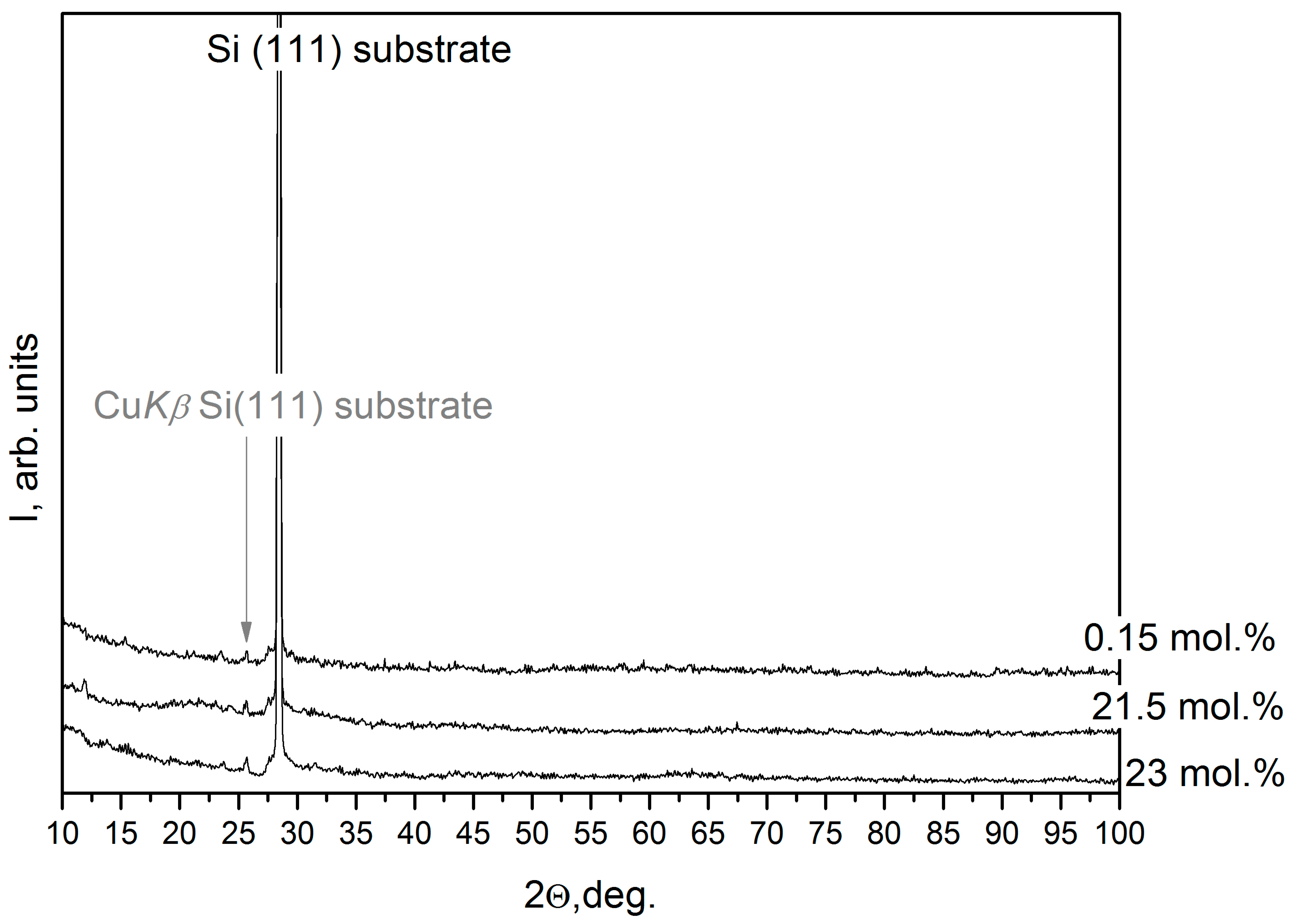
3.1. Analysis of the Presence of Amorphous Silicon Phase in a-SiOx:H + ncl-Si Films according to XRD, Raman and IR Spectroscopy

To assess the possibility of formation of silicon nanocrystals in a-SiOx:H + ncl-Si films, XRD patterns of the films obtained at an oxygen content of 0.15, 21.5 and 23 mol.% were obtained in the chamber of the process reactor (Figure 1).
Diffraction reflections at the angle of 2θ = 28.48° (d-spacing 3.13 Å) were detected in the XRD patterns of all the samples studied, which are associated with reflection from the crystallographic plane Si(111) from monocrystalline substrate (ICDD PDF-2 card No. 01–077-2110). Also, a low-intensity reflection was observed in XRD patterns at 2θ = 25.75°, associated with the reflection of Cu Kß radiation with a wavelength λ = 1.39 Å from the same crystallographic plane Si(111). The absence of other diffraction lines indicates the absence of long-range order (translational symmetry) in these a-SiOx:H + ncl-Si films, i.e., the films are X-ray amorphous.
Therefore, to establish the presence of an amorphous silicon phase in a-SiOx:H + ncl-Si films, Raman spectra were obtained (Figure 2a). Figure 2a clearly shows that in the sample with a minimum oxygen content (0.15 mol%), transverse optical (TO) modes at ∆v~480 cm−1 and longitudinal optical (LO) modes at ∆v~420 cm−1 are well observed, as well as transverse acoustic (TA) modes at ∆v~155 cm−1 and longitudinal acoustic (LA) modes at ∆v~310 cm−1, which is characteristic of the amorphous phase in silicon a-Si [35,36,37,38]. With an increase in the concentration of oxygen in the composition of the gas mixture from 0.15 to 23 mol.% in the Raman spectra of a-SiOx:H + ncl-Si films, the relative intensity of the optical mode of the TO (∆v~480 cm−1) decreases from ~0.2 to 0.01 rel. units, respectively. In addition, in the Raman spectra of all the films, a strong TO mode is observed at ∆v~521 cm−1, which in its position and half-width (5.5 cm−1) corresponds to the spectrum of single-crystal silicon (c-Si) [38]. Since, according to XRD data, silicon phases with translational symmetries were not detected in a-SiOx:H + ncl-Si films, the mode at ∆v~521 cm−1 occurs due to a monocrystalline silicon substrate. Thus, according to Raman spectroscopy data, the presence of an amorphous silicon phase was determined in a-SiOx:H + ncl-Si films.
Next, FTIR absorption spectra were obtained to determine the presence of hydrogen passivating the surface of silicon nanoclusters in a-SiOx:H + ncl-Si films (Figure 2b). From Figure 2b, it can be seen that in the IR spectra of the studied films, there are absorption peaks at ∆v = 610 cm−1, ∆v = 775 cm−1, ∆v = 865 cm−1 corresponding to the doubly degenerate bending vibrations of the H atom in the HSi-Si3-xOx group [39], stretching vibrations of the Si-H bond in the Si-O-Si-H group [39], and in the isolated SiH2 group [39], respectively. The presence of absorption peaks associated with Si-H groups in the FTIR spectra is quite expected and is due to the use of SiH4 silane in the production process of the film. In addition, in FTIR spectra of the films with a high oxygen content (21.5 and 23 mol.%), vibrations of the oxygen atom perpendicular to the plane of the Si-O-Si group (∆ν = 480 cm−1) are detected [39], stretching vibrations of the bridged oxygen in the plane of the Si-O-Si group (∆ν = 980 cm−1) [39], as well as the high-frequency “shoulder” of the main band of stretching vibrations of the Si-O bond of amorphous SiO2 containing no hydrogen (∆ν = 1120 cm−1) [39,40]. Thus, according to FTIR spectroscopy data, the presence of hydrogen necessary for passivation of the surface of amorphous silicon nanoclusters was detected in the studied a-SiOx:H + ncl-Si films, as well as the presence of Si-O bonds in the films obtained with a high oxygen concentration from 0.15 to 23 mol.% in the technological reactor of plasma chemical deposition.

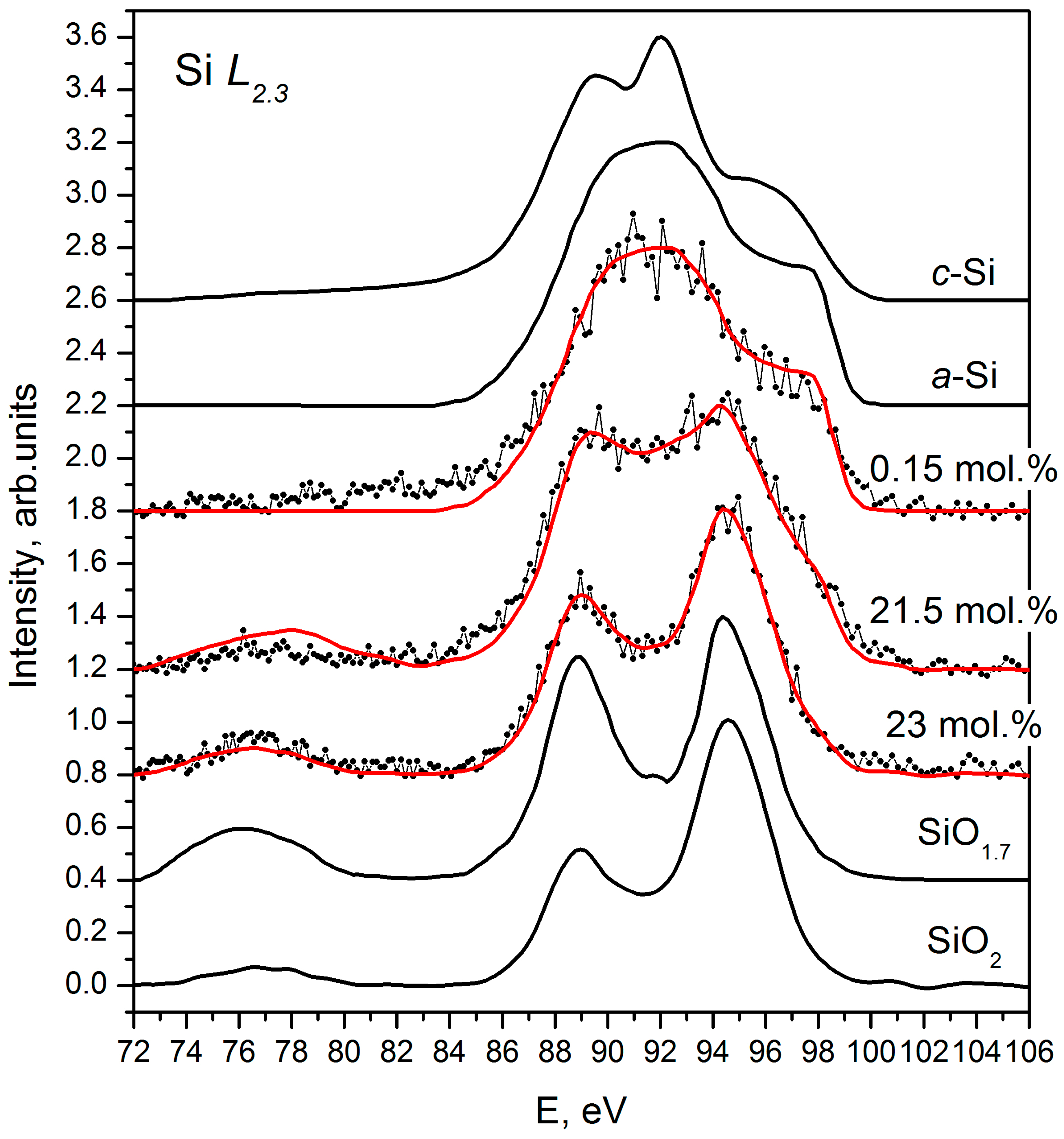
3.2. Analysis of the Phase Composition of a-SiOx:H + ncl-Si Films by the Ultra-Soft X-ray Emission Spectroscopy

To determine the phase composition of a-SiOx:H + ncl-Si films, the USXES method was applied, which allows determining the presence and ratio of crystalline (c-Si) and amorphous phases of silicon a-Si and a-SiOx. The X-ray emission Si L2.3 spectra of a-SiOx:H + ncl-Si films with silicon nanoclusters obtained by the USXES method are shown in Figure 3.
In the X-ray emission Si L2.3 spectrum of the a-SiOx:H + ncl-Si film obtained at a minimum oxygen concentration (0.15 mol%) in the reactor chamber, a broad intensive maximum is observed at E = 92 eV and a high density of electronic states near the valence band top Ev in the energy range E = 95 − 100 eV (Figure 3). These features of the spectrum are characteristic of amorphous silicon, and its spectrum is also shown in Figure 3 for comparison. This form of the X-ray emission spectrum of amorphous silicon a-Si is due to the blurring of the density of electronic states in the valence band compared with crystalline silicon c-Si (Figure 3). As a result of the lack of translational symmetry, disorder in the lengths and bond angles and breaking in the coordination number occur. With an increase in the oxygen concentration in the gas mixture up to 21.5 mol.%, the X-ray spectrum of the a-SiOx:H + ncl-Si film is strongly transformed and it includes two intensive peaks at E = 89 and E = 94.5 eV. The presence of these intensive maxima is due to the presence of Si 3s and 2p states and is characteristic of the SiO2 silicon dioxide spectrum (Figure 3) [31]. At the same time, some part of the density of the s-states of silicon appears in the energy region of the oxygen 2s orbital and this manifests itself as a long-wave satellite at E = 76 − 77 eV. However, the ratio of peak intensities at E = 89 and E = 94.5 eV in the spectrum of the a-SiOx:H + ncl-Si (21.5 moll.%) differs from the spectrum of silicon dioxide. The increase in the intensity of maximum at E = 89 eV is due to an increase in the contribution of Si 3s states as a result of an increase in the number of Si-Si bonds, which is typical for non-stoichiometric silicon oxides, as it is observed in the SiO1.7 spectrum (Figure 3) [31]. In addition, in the X-ray spectrum of the a-SiOx:H + ncl-Si film (21.5 mol.%), the intensity in the 92 eV region is 0.9 arb. units, which is noticeably higher than in the SiO2 spectrum (I = 0.35 arb. units) and even in the SiO1.7 spectrum (I = 0.4 arb. Units). Such an increase in the intensity of the spectrum at 92 eV is due to the presence of the a-SiOx:H + ncl-Si (21.5 mol.%) phase of non-oxidized silicon a-Si in the film, since its maximum in the spectrum is just in this energy region. A further increase in oxygen concentration in the gas mixture up to 23 mol.% leads to an increase in the intensity of the maxima at E = 89 and E = 94.5 eV in the X-ray emission Si L2.3 spectrum of a-SiOx:H + ncl-Si film (23 mol.%). At the same time, the ratio of intensities of these maxima corresponding to Si 3s (E = 89 eV) and O 2p (E = 94.5 eV) states approaches this spectrum to that of silicon dioxide, and a decrease in the intensity of the spectrum in the region of 92 eV to 0.5 arb. units indicates a significant decrease in the content of non-oxidized silicon a-Si in this film.
For more accurate determination of the phase composition from the obtained Si L2.3 spectra of a-SiOx:H + ncl-Si films, computer simulation of the valence band spectrum based on reference spectra was carried out according to the method described in [33]. The simulated spectra are shown in Figure 3 (red curves); the results of analysis of the phase composition of a-SiOx:H + ncl-Si films obtained at different concentrations of oxygen in the gas mixture, according to USXES data, are presented in Table 1.
According to the simulation results, the a-SiOx:H + ncl-Si film obtained at the minimum oxygen concentration in the reactor (0.15 mol.%) during PECVD deposition is an amorphous silicon film (Table 1), which is consistent with Raman spectroscopy data. An increase in the oxygen content in the composition of the gas mixture up to 21.5 mol.% leads to the formation of the film with a complex phase composition containing about 40% a-Si, as well as silicon suboxide SiO1.3 and silicon dioxide SiO2 (Table 1). Further increase in the oxygen content in the reactor atmosphere up to 23 mol.% leads to a significant decrease in the content of the amorphous silicon phase in the films to 15%, while the formation of silicon oxide phases SiO1.7 and SiO2, which are more oxygen-rich (Table 1), takes place. Since, according to the results of computer simulation, in the spectra of Si L2.3 a-SiOx:H + ncl-Si films (21.5 mol.% and 23 mol.%) the presence of various silicon suboxides was detected, the average oxidation state x of the SiOx suboxide matrix was calculated using the formula
x = i ( x i k i ) i k i ,
where xi- and ki- are the degree of oxidation and the relative content of the SiOx phase identified as a result of simulating of USXES spectra.
Evaluation of the average degree of oxidation of SiOx in a-SiOx:H + ncl-Si films (21.5 mol.% and 23 mol.%) allowed the detection of an increase in x for SiOx from ~1.5 to ~1.9 (that is, close to SiO2) with an increase in the oxygen content from 21.5 to 23 mol.% in the composition of the gas mixture during plasma chemical deposition.
Thus, according to USXES, the a-SiOx:H + ncl-Si film obtained with a minimum oxygen content in the gas mixture during plasma chemical sputtering is an amorphous silicon film that does not have translational symmetry, which is consistent with XRD and Raman spectroscopy data. An increase in oxygen concentration up to 21.5 mol.% leads to the formation of a composite film based on SiO1.3 silicon suboxide, SiO2 silicon dioxide and a sufficiently high content of amorphous silicon phase (40%). High content (45%) of the SiO1.3 phase in the composition of the a-SiOx:H + ncl-Si film (21.5 mol.%) explains a high intensity of the absorption peak corresponding to the vibrations of the H atom in the H-Si-Si3-xOx group and observed in the FTIR spectrum of this sample at ∆ν = 610 cm−1. With an increase in the oxygen content up to 23 mol.% in a-SiOx:H + ncl-Si films, the content of amorphous silicon a-Si decreases to 15%. On the contrary, the content of the SiO2 phase increases significantly to 55% and the formation of the SiO1.7 silicon suboxide phase is also observed. Thus, even a slight increase in oxygen concentration from 21.5 to 23 mol.% in the reactor chamber during PECVD deposition of a-SiOx:H + ncl-Si films from a SiH4 + Ar + O2 gas mixture with DC-discharge modulation leads to a decrease in the content of amorphous silicon from 40 to 15%. The average degree of oxidation of the suboxide matrix also increases from SiO1.5 to SiO1.9. In addition, according to USXES data, all silicon-based phases present in the studied a-SiOx:H + ncl-Si films do not have translational symmetry (amorphous), which is consistent with XRD and Raman spectroscopy data. According to [2], amorphous silicon is present in such films in the form of nanoclusters embedded in SiOx dielectric matrix and it possess photoluminescence. Therefore, further studies of the optical properties of a-SiOx:H + ncl-Si films were carried out.

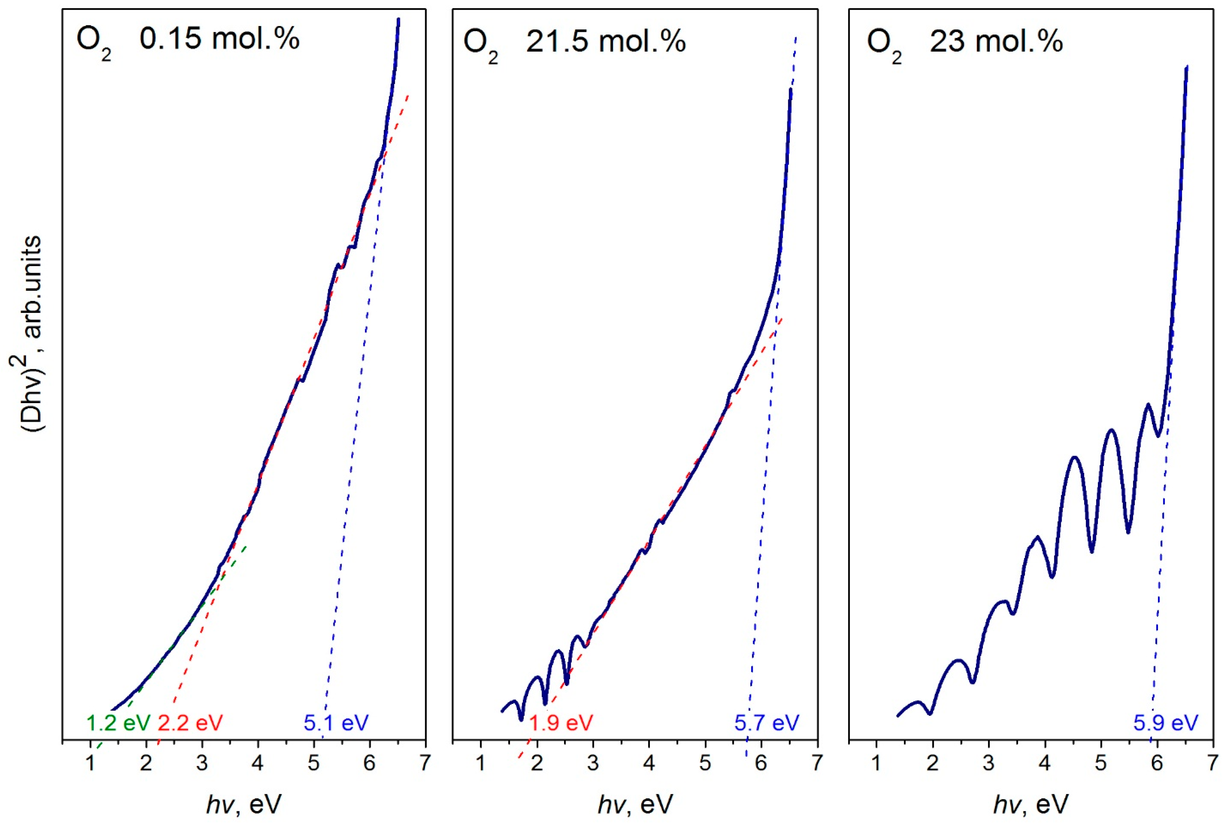
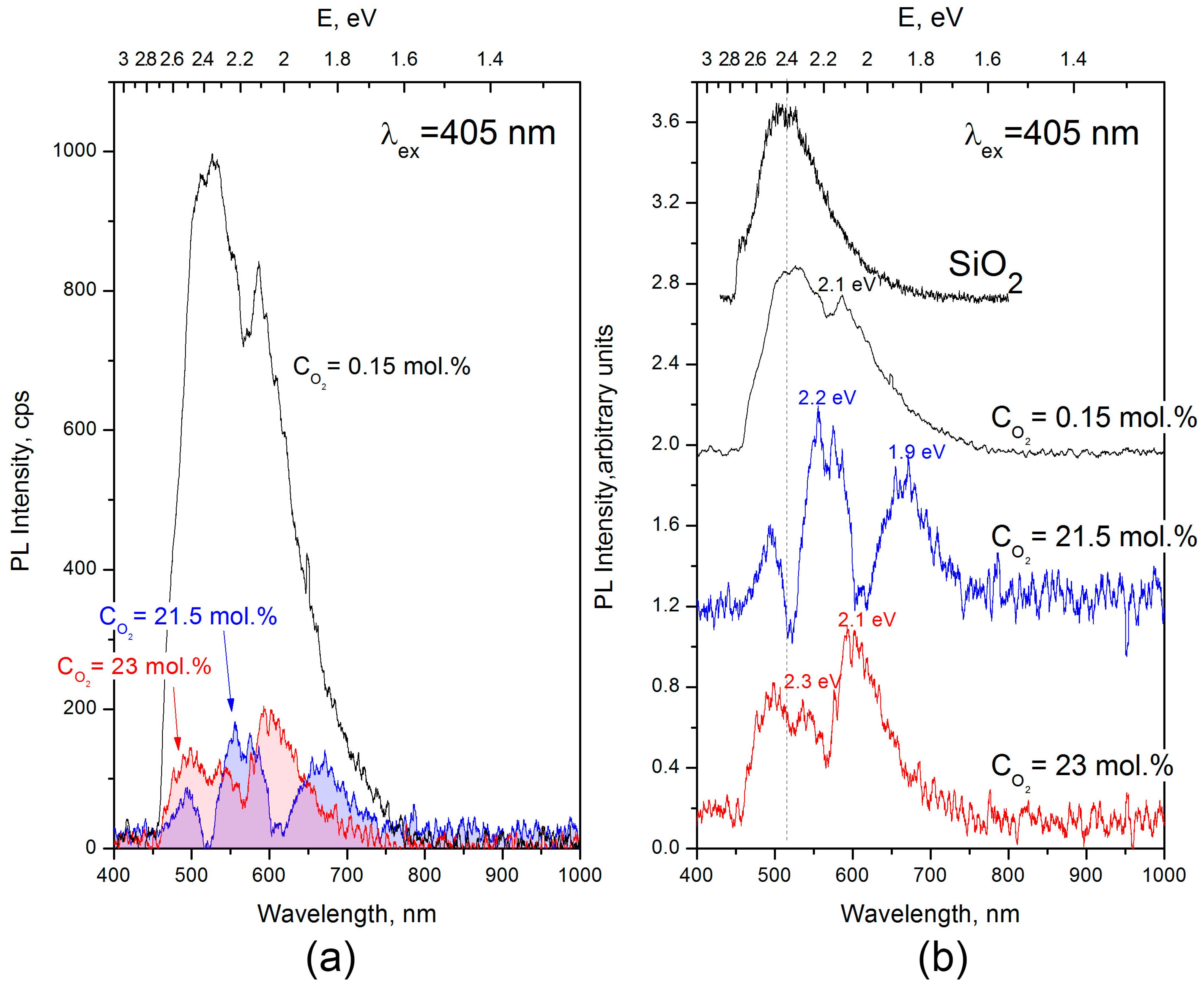
3.3. Optical Properties of a-SiOx:H + ncl-Si Films

Figure 4 shows the dependences of the optical absorption coefficient of a-SiOx:H + ncl-Si films obtained in a gas mixture with different oxygen content (0.15, 21.5, 23 mol.%) during plasma chemical deposition. For the a-SiOx:H + ncl-Si (0.15 mol.%) film, three linear sections are observed in the UV spectrum, and their extrapolation offers the following values of the optical band gap: 1.2, 2.2 and 5.1 eV (Figure 4). If the absorption edge at 1.2 eV corresponds to amorphous silicon, then the edge at 2.2 eV can be attributed to silicon nanoclusters of ~2 nm in size [3,27]. The high-energy absorption edge at 5.1 eV is due to the absorption of SiOx, suboxides present on the silicon surface. According to [41], the optical band gap of ~5 eV corresponds to the SiO1.8 suboxide. for the a-SiOx:H + ncl-Si (21.5 mol.%) film along with the interference pattern, two linear regions are observed in the optical absorption spectrum, and their extrapolation offers the optical band gap of 1.9 eV and 5.7 eV, which is due to the absorption of silicon nanoclusters with a size of ~3 nm [27,41] and a suboxide matrix [41], respectively. In the case of the a-SiOx:H + ncl-Si (23 mol.%) film, a strong interference pattern and one linear section are observed in the UV spectrum, and their extrapolation makes it possible to determine the optical band gap for SiO1.9 suboxide (5.9 eV) [41]. Assumption of the relationship of the absorption edges at hv~2.2 eV and hv~1.9 eV with silicon nanoclusters of ~2–3 nm in size is consistent with the presence of photoluminescence (PL) bands in the energy range of ~2.3–1.9 eV (Figure 5). At the same time, in the PL spectrum of the a-SiOx:H + ncl-Si (0.15 mol.%) film, the main maximum in accordance with its position and half-width is close to the PL spectrum of silicon oxide SiO2 (defect related luminescence in SiO2 network). This is clearly seen in Figure 5b (black curve), where the normalized PL spectra are presented. In turn, the presence of the additional maximum of PL at 2.1 eV correlates with UV spectroscopy data, where a direct transition was detected for this sample at hv~2.2 eV, and this may be due to the luminescence of silicon nanoclusters with a size of ~2 nm [3,27]. However, the intensity of this maximum is quite low, i.e., the main contribution to the PL spectrum of this sample is offered by silicon oxide defects. Increasing oxygen content in the process reactor chamber to 21.5 mol.% leads to the transformation of the PL spectrum with the appearance of pronounced PL bands at 2.2 and 1.9 eV (Figure 5b, blue curve). There is also a decrease in photoluminescence intensity, despite the high content of silicon nanoclusters in the film (40%), which is clearly seen in Figure 5a (blue curve). Such decrease in PL may be due to a high content of the SiO1.3 phase in the dielectric matrix (detected according to USXES data) with a large number of defects that are the centers of non-radiative recombination. The presence of PL bands in the a-SiOx:H + ncl-Si (21.5 mol.%) film at 2.2 and 1.9 eV is consistent with UV spectroscopy data, and indicates the formation of two arrays of nanoclusters in the film with average sizes of ~2 and ~3 nm [3,27,41]. Further increase in the oxygen content up to 23 mol.% in the composition of the gas mixture during plasma chemical deposition leads to a short-wave shift of the PL peaks to ~2.3 and ~2.1 eV (Figure 5b), which may be due to a decrease in the size of silicon nanoclusters to ~1.5–2 nm [3,27,41]. In addition, despite the low content of silicon nanoclusters (15%) in this sample, there is no noticeable decrease in the intensity of the PL spectrum compared to the a-SiOx:H + ncl-Si (21.5 mol.%) sample (Figure 5a). This may be due to the presence of SiO2 and SiO1.7 phases (with a higher symmetry of silicon–oxygen tetrahedra and, as a consequence, a lower defect content compared to the SiO1.3 phase) being a part of the dielectric matrix. Thus, nonlinear qualitative and quantitative changes in the phase composition of a-SiOx:H + ncl-Si films under the influence of oxygen lead to a short-wave shift of the PL peaks.

4. Conclusions

The results of complex studies showed that during the PECVD deposition of a-SiOx:H + ncl-Si films from a SiH4 + Ar + O2 gas mixture with a DC-discharge modulation under oxygen content of 0.15 mol.% in the atmosphere of the process reactor, amorphous silicon film is formed that does not have translational symmetry.
An increase in the oxygen concentration in the composition of the gas mixture up to 21.5 mol.% leads to the formation of a composite film based on SiO1.3 silicon suboxide, SiO2 silicon dioxide with a sufficiently high content of amorphous silicon phase (40%). At the same time, the average degree of oxidation x in the SiOx suboxide matrix is ~1.5.
Even a slight increase in oxygen concentration from 21.5 to 23 mol.% in the reactor chamber during PECVD deposition of a-SiOx:H + ncl-Si films from a SiH4 + Ar + O2 gas mixture with a DC-discharge modulation leads to not only a decrease in the content of amorphous silicon from 40 to 15%, but also an increase in the average degree of oxidation of the suboxide matrix from SiO1.5 to SiO1.9.
According to USXES data, all silicon-based phases present in the studied a-SiOx:H + ncl-Si films do not have translational symmetry, i.e., they are amorphous, which is consistent with XRD and Raman spectroscopy data. At the same time, according to FTIR spectroscopy data, the presence of hydrogen necessary for passivation of the surface of amorphous silicon nanoclusters was detected in the studied a-SiOx:H + ncl-Si films.
All a-SiOx:H + ncl-Si films have optical absorption edges in the energy range of ~2 eV and ≥5 eV due to silicon nanoclusters of ~2–3 nm in size and a suboxide dielectric matrix, respectively. In the PL spectra of a-SiOx:H + ncl-Si films, there are also PL bands in the range of ~1.9–2.3 eV associated with photoluminescence of amorphous silicon nanoclusters.
The PL spectrum of the a-SiOx:H + ncl-Si film (21.5 mol.%) exhibits pronounced maxima at 2.2 and 1.9 eV; their presence is due to the luminescence of nanoclusters with average sizes of ~2 and ~3 nm. Further increase in the oxygen content to 23 mol.% in the composition of the gas mixture during PECVD deposition leads to a short-wave shift of the PL peaks to ~2.3 and ~2.1 eV, respectively, that is associated with a decrease in the size of silicon nanoclusters to ~1.5–2 nm.

Author Contributions

Conceptualization, V.A.T.; methodology, V.A.T. and K.A.B.; software, K.A.B.; validation, A.N.L.; formal analysis, K.A.B., P.V.S. and V.A.T.; investigation, E.I.T., Y.K.U., N.A.K., S.A.I., D.N.N., D.L.G., D.A.M., E.V.P. and I.N.T.; writing—original draft preparation, K.A.B. and V.A.T.; writing—review and editing, P.V.S., K.A.B. and V.A.T.; visualization, E.V.P.; supervision, V.A.T.; project administration, V.A.T.; funding acquisition, V.A.T. All authors have read and agreed to the published version of the manuscript.

Funding

The work was carried out under the support of the Ministry of Science and Higher Education of Russian Federation provided by the grand No. FZGU-2023-0006. The study was supported by the Ministry of Science and Higher Education of Russia under Agreement N 075-15-2021-1351 in part of ultra-soft X-ray emission spectroscopy.

Data Availability Statement

The data are available from the author on request via e-mail.

Acknowledgments

The results of research were partially obtained with the use of equipment of the Center for Collective Use of Voronezh State University. URL: http://ckp.vsu.ru (accessed on 1 March 2023).

Conflicts of Interest

The author declares no conflict of interest.

References

  1. Kim, K.H.; Johnson, E.V.; Kazanskii, A.G.; Khenkin, M.V.; Roca, P. Unravelling a Simple Method for the Low Temperature Synthesis of Silicon Nanocrystals and Monolithic Nanocrystalline Thin Films. Sci. Rep. 2017, 7, 40553. [Google Scholar] [CrossRef] [PubMed]
  2. Undalov, Y.K.; Terukov, E.I.; Trapeznikova, I.N. Formation of Ncl-Si in the Amorphous Matrix a-SiOx:H Located near the Anode and on the Cathode, Using a Time-Modulated DC Plasma with the (SiH4–Ar–O2) Gas Phase (Co2=21.5mol%). Semiconductors 2019, 53, 1514–1523. [Google Scholar] [CrossRef]
  3. Fauchet, P.M. Light Emission from Si Quantum Dots. Mater. Today 2005, 8, 26–33. [Google Scholar] [CrossRef]
  4. Ledoux, G.; Gong, J.; Huisken, F.; Guillois, O.; Reynaud, C. Photoluminescence of Size-Separated Silicon Nanocrystals: Confirmation of Quantum Confinement. Appl. Phys. Lett. 2002, 80, 4834–4836. [Google Scholar] [CrossRef]
  5. Richter, L.J.; Ross, U.; Seibt, M.; Ihlemann, J. Excimer Laser Surface Patterning for Photoluminescence Enhancement of Silicon Nanocrystals. Photonics 2023, 10, 358. [Google Scholar] [CrossRef]
  6. Comedi, D.; Zalloum, O.H.Y.; Wojcik, J.; Mascher, P. Light Emission from Hydrogenated and Unhydrogenated Si-Nanocrystal/Si Dioxide Composites Based on PECVD-Grown Si-Rich Si Oxide Films. IEEE J. Sel. Top. Quantum Electron. 2006, 12, 1561–1569. [Google Scholar] [CrossRef]
  7. González-Fernández, A.A.; Aceves-Mijares, M.; Pérez-Díaz, O.; Hernández-Betanzos, J.; Domínguez, C. Embedded Silicon Nanoparticles as Enabler of a Novel Cmos-Compatible Fully Integrated Silicon Photonics Platform. Crystals 2021, 11, 630. [Google Scholar] [CrossRef]
  8. Tapia Burgos, J.A.; Mahr, C.; Olaya, A.R.S.; Robben, L.; Schowalter, M.; Rosenauer, A.; Wittstock, G.; Wittstock, A.; Bäumer, M. The Impact of the Manufacturing and Corrosion Steps of the AuCu Master Alloy on the Catalytic Activity of Nanoporous Gold for CO Oxidation. SSRN Electron. J. 2021, 3955671. [Google Scholar] [CrossRef]
  9. Nikolskaya, A.A.; Korolev, D.S.; Trushin, V.N.; Yunin, P.A.; Mikhaylov, A.N.; Belov, A.I.; Konakov, A.A.; Okulich, E.V.; Pavlov, D.A.; Tetelbaum, D.I. Photoluminescent Properties of the SiO2/Si System with Ion-Synthesized Hexagonal Silicon of the 9R-Si Phase: Effect of Post-Implantation Annealing. Nucl. Instrum. Methods Phys. Res. Sect. B Beam Interact. Mater. Atoms 2023, 537, 60–64. [Google Scholar] [CrossRef]
  10. Taheri, M.; Mansour, N. Silicon Nanoparticles Produced by Two-Step Nanosecond Pulsed Laser Ablation in Ethanol for Enhanced Blue Emission Properties. Silicon 2020, 12, 789–797. [Google Scholar] [CrossRef]
  11. Patrone, L.; Nelson, D.; Safarov, V.I.; Sentis, M.; Marine, W.; Giorgio, S. Photoluminescence of Silicon Nanoclusters with Reduced Size Dispersion Produced by Laser Ablation. J. Appl. Phys. 2000, 87, 3829–3837. [Google Scholar] [CrossRef]
  12. Ishikawa, Y.; Shibata, N.; Fukatsu, S. Fabrication of Highly Oriented Si:SiO2 Nanoparticles Using Low Energy Oxygen Ion Implantation during Si Molecular Beam Epitaxy. Appl. Phys. Lett. 1996, 68, 2249–2251. [Google Scholar] [CrossRef]
  13. Nikitin, T.; Khriachtchev, L. Optical and Structural Properties of Si Nanocrystals in SiO2 Films. Nanomaterials 2015, 5, 614–655. [Google Scholar] [CrossRef] [PubMed]
  14. Kang, Z.T.; Arnold, B.; Summers, C.J.; Wagner, B.K. Synthesis of Silicon Quantum Dot Buried SiOx Films with Controlled Luminescent Properties for Solid-State Lighting. Nanotechnology 2006, 17, 4477–4482. [Google Scholar] [CrossRef]
  15. Liu, B.; Sun, J.; Zhou, L.; Zhang, P.; Yan, C.; Fu, Q. Microstructure Evolution and Growth Mechanism of Core-Shell Silicon-Based Nanowires by Thermal Evaporation of SiO. J. Adv. Ceram. 2022, 11, 1417–1430. [Google Scholar] [CrossRef]
  16. He, M.; Yang, D.; Li, D. Electroluminescence from Metal–Oxide–Semiconductor Devices Based on Erbium Silicate Nanocrystals and Silicon Nanocrystals Co-Embedded in Silicon Oxide Thin Films. J. Mater. Sci. Mater. Electron. 2021, 32, 20659–20667. [Google Scholar] [CrossRef]
  17. Adhikari, D.; Junda, M.M.; Grice, C.R.; Marsillac, S.X.; Collins, R.W.; Podraza, N.J. N-i-p Nanocrystalline Hydrogenated Silicon Solar Cells with RF-Magnetron Sputtered Absorbers. Materials 2019, 12, 1699. [Google Scholar] [CrossRef]
  18. Comedi, D.; Zalloum, O.H.Y.; Irving, E.A.; Wojcik, J.; Roschuk, T.; Flynn, M.J.; Mascher, P. X-Ray-Diffraction Study of Crystalline Si Nanocluster Formation in Annealed Silicon-Rich Silicon Oxides. J. Appl. Phys. 2006, 99, 023518. [Google Scholar] [CrossRef]
  19. Qin, G.; Qin, G. Photoluminescence Mechanism Model for Oxidized Porous Silicon and Nanoscale-Silicon-Particle-Embedded Silicon Oxide. Phys. Rev. B Condens. Matter Mater. Phys. 2003, 68, 085309. [Google Scholar] [CrossRef]
  20. Puzder, A.; Williamson, A.J.; Grossman, J.C.; Galli, G. Surface Chemistry of Silicon Nanoclusters. Phys. Rev. Lett. 2002, 88, 4. [Google Scholar] [CrossRef]
  21. Daldosso, N.; Das, G.; Larcheri, S.; Mariotto, G.; Dalba, G.; Pavesi, L.; Irrera, A.; Priolo, F.; Iacona, F.; Rocca, F. Silicon Nanocrystal Formation in Annealed Silicon-Rich Silicon Oxide Films Prepared by Plasma Enhanced Chemical Vapor Deposition. J. Appl. Phys. 2007, 101, 113510. [Google Scholar] [CrossRef]
  22. Mandracci, P.; Rivolo, P. Silicon-Based Thin Films and Nanostructures. Coatings 2023, 13, 1075. [Google Scholar] [CrossRef]
  23. Zamchiy, A.O.; Baranov, E.A.; Merkulova, I.E.; Khmel, S.Y.; Maximovskiy, E.A. Determination of the Oxygen Content in Amorphous SiOx Thin Films. J. Non. Cryst. Solids 2019, 518, 43–50. [Google Scholar] [CrossRef]
  24. Wang, X.X.; Zhang, J.G.; Ding, L.; Cheng, B.W.; Ge, W.K.; Yu, J.Z.; Wang, Q.M. Origin and Evolution of Photoluminescence from Si Nanocrystals Embedded in a SiO2 Matrix. Phys. Rev. B Condens. Matter Mater. Phys. 2005, 72, 195313. [Google Scholar] [CrossRef]
  25. Gusev, O.B.; Poddubny, A.N.; Prokofiev, A.A.; Yassievich, I.N. Light Emission from Silicon Nanocrystals. Semiconductors 2013, 47, 183–202. [Google Scholar] [CrossRef]
  26. Yi, L.X.; Heitmann, J.; Scholz, R.; Zacharias, M. Si Rings, Si Clusters, and Si Nanocrystals—Different States of Ultrathin SiOx Layers. Appl. Phys. Lett. 2002, 81, 4248–4250. [Google Scholar] [CrossRef]
  27. Delerue, C.; Allan, G.; Lannoo, M. Optical Band Gap of Si Nanoclusters. J. Lumin. 1998, 80, 65–73. [Google Scholar] [CrossRef]
  28. Fang, Y.C.; Li, W.Q.; Qi, L.J.; Li, L.Y.; Zhao, Y.Y.; Zhang, Z.J.; Lu, M. Photoluminescence from SiOx Thin Films: Effects of Film Thickness and Annealing Temperature. Nanotechnology 2004, 15, 494–500. [Google Scholar] [CrossRef]
  29. Hofmeister, H.; Kahler, U. Si Nanocrystallites in SiOx Films by Vapour Deposition and Thermal Processing. In Silicon Chemistry: From the Atom to Extended Systems; Wiley: Hoboken, NJ, USA, 2007; pp. 252–268. [Google Scholar] [CrossRef]
  30. Hirata, A.; Kohara, S.; Asada, T.; Arao, M.; Yogi, C.; Imai, H.; Tan, Y.; Fujita, T.; Chen, M. Atomic-Scale Disproportionation in Amorphous Silicon Monoxide. Nat. Commun. 2016, 7, 11591. [Google Scholar] [CrossRef]
  31. Wiech, G.; Feldhütter, H.O.; Šimůnek, A. Electronic Structure of Amorphous SiOx:H Alloy Films Studied by x-Ray Emission Spectroscopy: Si K, Si L, and O K Emission Bands. Phys. Rev. B 1993, 47, 6981–6989. [Google Scholar] [CrossRef]
  32. Agarwal, B.K. Soft X-Ray Spectroscopy. In X-Ray Spectroscopy. Springer Series in Optical Sciences; Springer: Berlin/Heidelberg, Germany, 1979; ISBN 978-3-540-50719-2. [Google Scholar]
  33. Terekhov, V.A.; Kashkarov, V.M.; Manukovskii, E.Y.; Schukarev, A.V.; Domashevskaya, E.P. Determination of the Phase Composition of Surface Layers of Porous Silicon by Ultrasoft X-Ray Spectroscopy and X-Ray Photoelectron Spectroscopy Techniques. J. Electron Spectros. Relat. Phenom. 2001, 114–116, 895–900. [Google Scholar] [CrossRef]
  34. Shulakov, A.S. X-Ray Emission Depth-Resolved Spectroscopy for Investigation of Nanolayers. J. Struct. Chem. 2011, 52, 1–12. [Google Scholar] [CrossRef]
  35. Ivanda, M.; Hohl, A.; Montagna, M.; Mariotto, G.; Ferrari, M.; Crnjak Orel, Z.; Turković, A.; Furić, K. Raman Scattering of Acoustical Modes of Silicon Nanoparticles Embedded in Silica Matrix. J. Raman Spectrosc. 2006, 37, 161–165. [Google Scholar] [CrossRef]
  36. Ivanda, M. Raman Spectroscopy of Porous Silicon. In Handbook of Porous Silicon: Second Edition; Springer: Cham, Switzerland, 2018; Volume 1–2, pp. 611–620. ISBN 9783319713816. [Google Scholar]
  37. Li, Z.; Li, W.; Jiang, Y.; Cai, H.; Gong, Y.; He, J. Raman Characterization of the Structural Evolution in Amorphous and Partially Nanocrystalline Hydrogenated Silicon Thin Films Prepared by PECVD. J. Raman Spectrosc. 2011, 42, 415–421. [Google Scholar] [CrossRef]
  38. Iqbal, Z.; Vepřek, S.; Webb, A.P.; Capezzuto, P. Raman Scattering from Small Particle Size Polycrystalline Silicon. Solid State Commun. 1981, 37, 993–996. [Google Scholar] [CrossRef]
  39. Lucovsky, G.; Yang, J.; Chao, S.S.; Tyler, J.E.; Czubatyj, W. Oxygen-Bonding Environments in Glow-Discharge-Deposited Amorphous Silicon-Hydrogen Alloy Films. Phys. Rev. B 1983, 28, 3225–3233. [Google Scholar] [CrossRef]
  40. Galeener, F.L.; Lucovsky, G. Longitudinal Optical Vibrations in Glasses: GeO2 and SiO2. Phys. Rev. Lett. 1976, 37, 1474–1478. [Google Scholar] [CrossRef]
  41. Barranco, A.; Yubero, F.; Espinós, J.P.; Groening, P.; González-Elipe, A.R. Electronic State Characterization of SiOx Thin Films Prepared by Evaporation. J. Appl. Phys. 2005, 97, 1927278. [Google Scholar] [CrossRef]
Figure 1. XRD patterns of PECVD a-SiOx:H + ncl-Si films obtained at different oxygen concentrations in the composition of a SiH4 + Ar + O2 gas mixture.
Symmetry 15 01800 g001
Figure 2. Raman (a) and FTIR absorption (b) spectra of c-Si, a-Si etalons and PECVD a-SiOx:H + ncl-Si films obtained at different oxygen concentrations in the composition of SiH4 + Ar + O2 gas mixture.
Symmetry 15 01800 g002
Figure 3. Ultra-soft X-ray emission Si L2.3 spectra of PECVD a-SiOx:H + ncl-Si films obtained at different oxygen concentrations in the composition of a SiH4 + Ar + O2 gas mixture and reference samples of amorphous silicon a-Si, silicon dioxide SiO2 and silicon suboxide SiO1.7 [31].
Symmetry 15 01800 g003
Figure 4. UV spectra of PECVD a-SiOx:H + ncl-Si films obtained at different oxygen concentrations in the composition of a SiH4 + Ar + O2 gas mixture.
Symmetry 15 01800 g004
Figure 5. PL spectra of PECVD a-SiOx:H + ncl-Si films obtained at different oxygen concentrations in the composition of a SiH4 + Ar + O2 gas mixture, represented in the scale of absolute (a) and relative (b) intensity of the spectra.
Symmetry 15 01800 g005
Table 1. Phase composition of PECVD a-SiOx:H + ncl-Si films obtained at different oxygen concentrations in the composition of a SiH4 + Ar + O2 gas mixture, according to USXES data.
Oxygen Concentrations in the SiH4 + Ar + O2
Gas Mixture
Phase Compositionx in SiOx
a-SiSiO1.3SiO1.7SiO2Error
0.15 mol.%100%---5%-
21.5 mol.%40%45%-15%~1.5
23 mol.%15%-30%55%~1.9
Disclaimer/Publisher’s Note: The statements, opinions and data contained in all publications are solely those of the individual author(s) and contributor(s) and not of MDPI and/or the editor(s). MDPI and/or the editor(s) disclaim responsibility for any injury to people or property resulting from any ideas, methods, instructions or products referred to in the content.

