Article

Effect of the Growth Interruption on the Surface Morphology and Crystalline Quality of MOCVD-Grown h-BN

1
Research and Development Center for Solid State Lighting, Institute of Semiconductors, Chinese Academy of Sciences, Beijing 100083, China
2
College of Electronic, Electrical and Communication Engineering, University of Chinese Academy of Sciences, Beijing 101408, China
3
Key Laboratory of Semiconductor Materials Science, Institute of Semiconductors, Chinese Academy of Sciences, Beijing 100083, China
4
Key Laboratory for Physical Electronics and Devices of Ministry of Education and Shaanxi Provincial Key Laboratory of Photonics & Information Technology, Xi’an Jiaotong University, Xi’an 710049, China
*
Authors to whom correspondence should be addressed.
Crystals 2023, 13(3), 486; https://doi.org/10.3390/cryst13030486
Submission received: 20 February 2023 / Revised: 6 March 2023 / Accepted: 10 March 2023 / Published: 11 March 2023
(This article belongs to the Special Issue Wide-Bandgap Semiconductors)

Abstract

:
Hexagonal boron nitride (h-BN) is one promising material class for applications in DUV optoelectronics due to the layered structure and ultra-wide bandgap. The synthesis of h-BN with smooth surface morphology and high quality on dielectric substrates is the key to construct efficient functional devices thereon. In this study, we reported wafer-scale h-BN on c-plane sapphire substrates by metal organic chemical vapor deposition utilizing the flow modulation epitaxy (FME) with growth interruptions. The effect of the growth interruption location within FME on the surface morphology and crystalline quality of h-BN films was systematically investigated. The interruption after the TEB injection could promote the mobility of B adatoms, and the interruption after the NH3 injection could further relieve the passivation of N terminal growth fronts and mitigate the parasitic gas-phase reaction between growth precursors. By simultaneously employing interruptions after TEB and NH3 injections, the growth rate of h-BN increased significantly from 0.16 nm/min to 4.76 nm/min, and the surface roughness of 2-nm-thick h-BN was reduced to 0.587 nm. In addition, h-BN grown with an interruption solely after the NH3 injection presented the best crystallinity because the relatively slow growth rate reduced the possibility of impurity incorporation.

1. Introduction

Hexagonal boron nitride (h-BN) has attracted extensive attention in the fields of photoelectronics and beyond in recent years. The B and N atoms are connected by sp2 hybridized covalent bonds within the c-plane to form a graphite-like honeycomb structure, while the interlayers are bounded by weak van der Waals force [1,2,3]. Thanks to the special 2D layer structure and good chemical and thermal stability, van der Waals heterojunctions such as h-BN/graphene [4] and TMD/h-BN [5] have been successfully exhibited to realize atomically thin integrated circuitry [6,7]. In addition, the wide bandgap (~6 eV [8,9,10]) enables BN to be applied to deep-ultraviolet high-reflectivity distributed Bragg reflectors (DBRs) [11], light emitting diodes [12,13], photon detectors [14,15,16] and single-photon sources (SPS) [17,18].
Several deposition methods have been studied to prepare h-BN films with high crystal quality and smooth surface morphology, mainly including chemical vapor deposition (CVD), molecular beam epitaxy (MBE) [10], sputtering [19] and metal organic chemical vapor deposition (MOCVD) [20]. Among them, MOCVD can be used to attain high-quality wafer-level h-BN with controllable thickness (1.5 nm–1.7 µm) [20,21,22,23]. Furthermore, it makes the growth of h-BN compatible with other Ⅲ-nitride semiconductors and simplifies the epitaxial growth of III-nitride devices. Triethylboron (TEB) and ammonia (NH3) are commonly used as the growth precursors. Under a conventional continuous MOCVD growth mode, the growth rate of h-BN is quite limited due to the parasitic reactions between the growth precursors and the self-terminating effect because of the Langmuir-Hinshelwood mechanism [23,24]. To address the problems, flow modulation epitaxy (FME) [25,26,27], that is, TEB and NH3 are alternately supplied to the sample surface, has been developed. Kobayashi et al. reported that the growth rate of h-BN was improved by 10 times using the FME mode [25]. Yang et al. studied the dependence of crystal quality and surface morphology of h-BN layers on the precursor injection durations, and found that the optimized FME condition was when just enough NH3 was supplied to fully convert the TEB within one cycle [27]. Nonetheless, there are still parasitic reactions due to intermix of TEB and NH3 at switching times; islands appear on the BN surface because of the limited surface migration of B adatoms [25]. Jiang et al. claimed that introducing growth interruptions within the FME process could mitigate parasitic gas phase reactions and encourage adatoms to find equilibrium positions [28]. Kim et al. explored the role of the carrier gas on the characteristics of h-BN films grown in such modified FME mode, and proved that the crystallinity of h-BN was improved by using H2 carrier gas because of more effective etching and regrowth processes [29]. Then they optimized the growth pressure, and concluded that an appropriate pressure could reduce the generation of the defects like nitrogen vacancies and grain boundaries [30]. However, the strategy to introduce the interruption within FME was barely discussed. In this work, we tuned the growth interruption location within FME and investigated the effects on the growth rate, the surface morphology, and the crystal quality of h-BN. It was found that the growth rate of h-BN was significantly enhanced by introducing a growth interruption after the TEB injection due to the improved surface migration of B adatoms, and further employing a growth interruption after the NH3 injection could obtain better surface smoothness thanks to the effective remission of parasitic reactions. The h-BN film with best crystallinity was achieved when solely introducing a growth interruption after the NH3 injection, which was attributed to the low-concentration impurity incorporation.

2. Materials and Methods

The h-BN films were grown on 2-in. c-plane sapphire substrates using a home-made high-temperature vertical showerhead MOCVD system. Triethylboron (TEB), NH3 and H2 were used as the B precursor, N precursor, and the carrier gas, respectively. The supply rates of TEB and NH3 were fixed at 30 sccm and 2000 sccm, respectively. The growth pressure was 50 torr and the growth temperature was 1250 °C. Four FME modes with different growth interruption locations were implemented. As shown in Figure 1a, the FME mode without growth interruptions denoted as NH3/TEB consists of two steps: (1) NH3 injection for 4 s, (2) TEB injection for 2 s. Figure 1b–d illustrate the other three FME modes with 1 s growth interruption after NH3 injection (NH3/Itrp/TEB), after TEB injection (NH3/TEB/Itrp), and simultaneously after NH3 and TEB injections (NH3/Itrp/TEB/Itrp), respectively. During the growth interruption period, only H2 was allowed into the reactor.
The surface morphology of h-BN films was investigated by scanning electron microscopy (SEM) (Hitachi, Tokyo, Japan; operated at 4.4 kV) and atomic force microscopy (AFM) (D3100, Veeco, New York, NY, USA). The thickness was estimated using the spectroscopic ellipsometer (Horiba scientific, UVISEL PLUS, London, UK). The chemical identity of h-BN films was analyzed according to the infrared reflectance spectra using Fourier transform infrared spectroscopy (FTIR, PerkinElmer Frontier, Waltham, MA, USA) and X-ray photoelectron spectroscopy (XPS, ESCALAB 250Xi, Thermo Scientific, Waltham, MA, USA, using a monochromatic Al Kα X-ray source). The crystalline properties were assessed by high resolution X-ray diffraction (HRXRD, Bede D1, Durham, UK) using Cu Kα radiation (λ = 1.5406 Å) and Raman spectroscope using a 532-nm excitation source (Horiba, Kyoto, Japan). The optical properties were measured by UV-VIS transmission spectrometry (TU-1901 Spectrophotometer, PURSEE, Beijing, China). The defect-related trap states were characterized by photoluminescence with 325 nm laser source (Horiba, Kyoto, Japan).

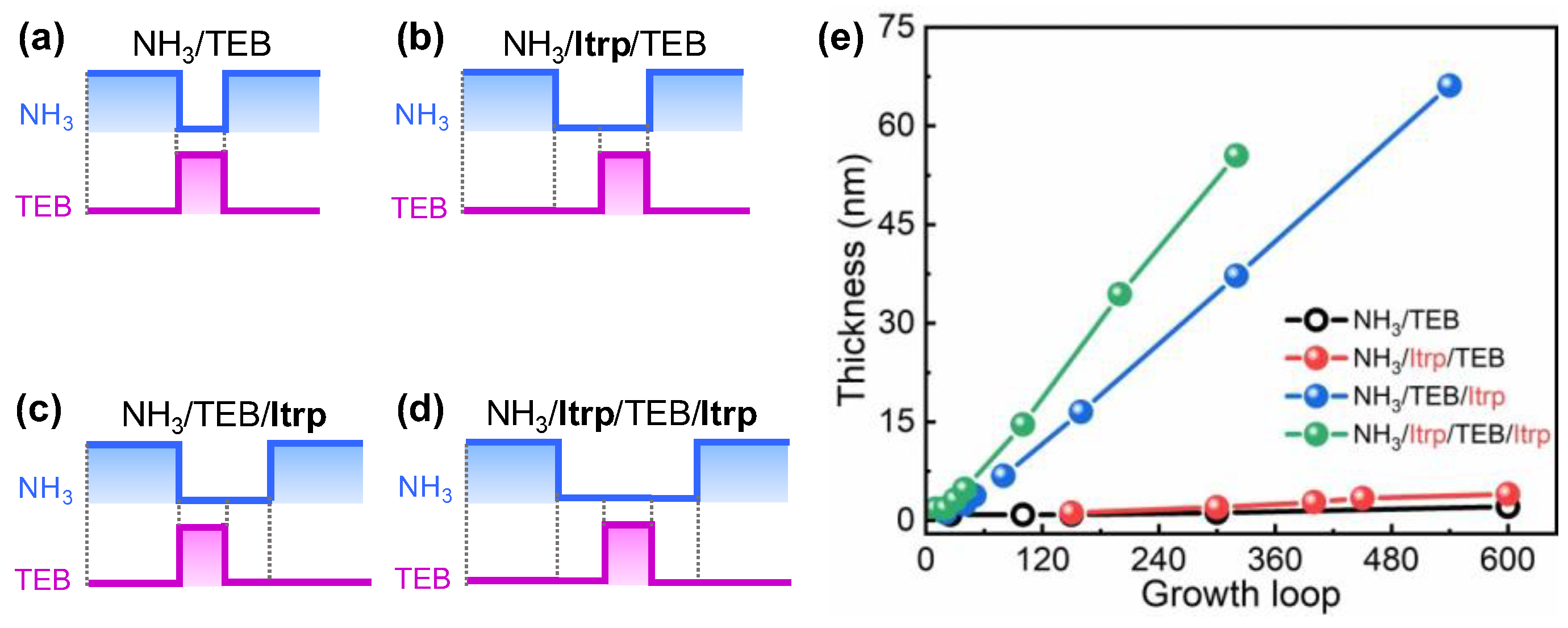
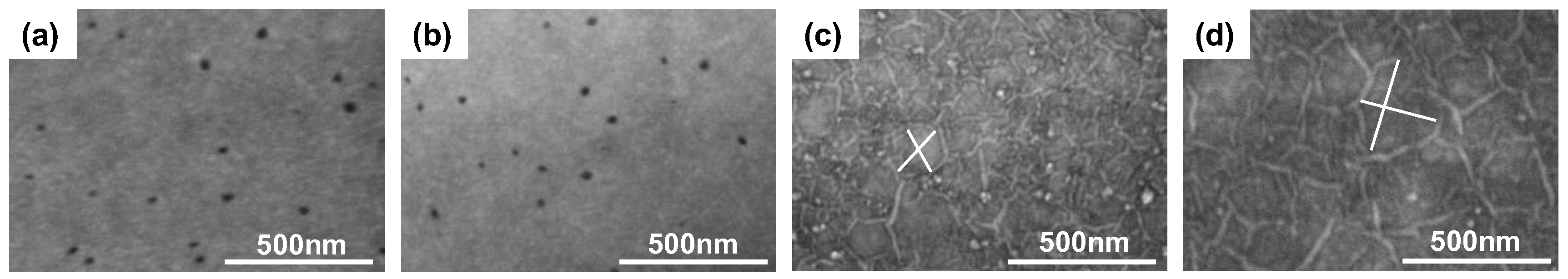
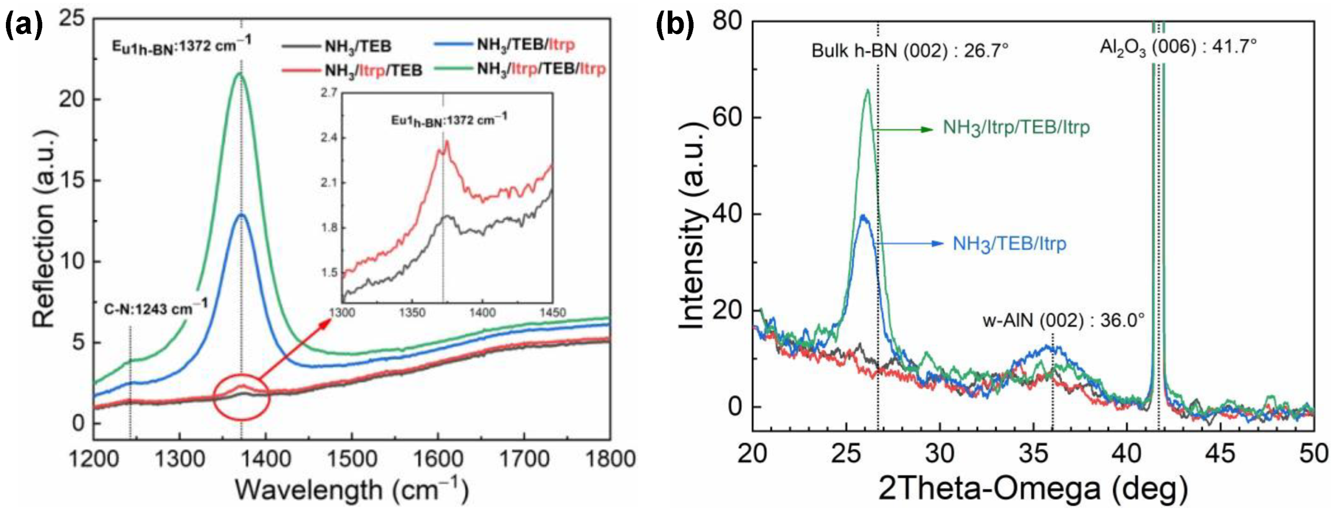
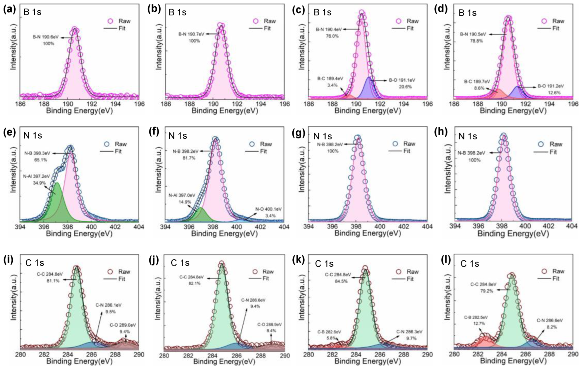
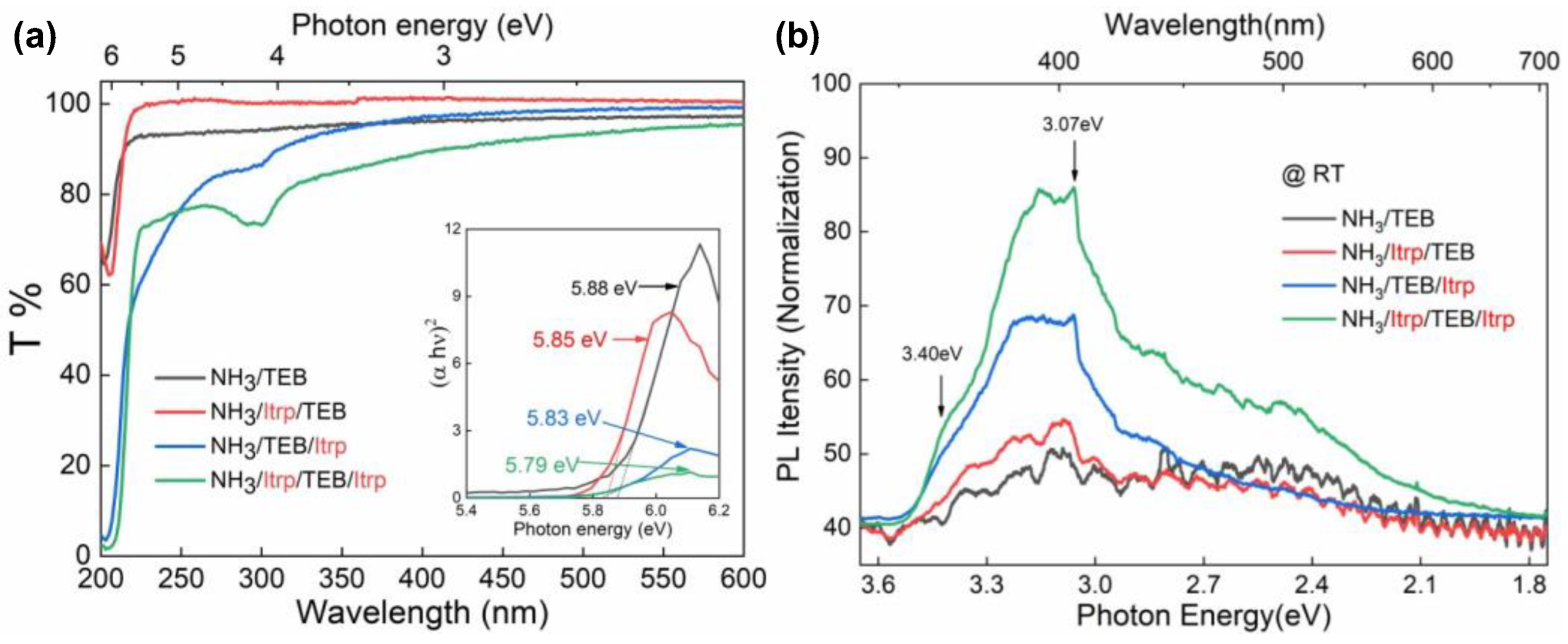
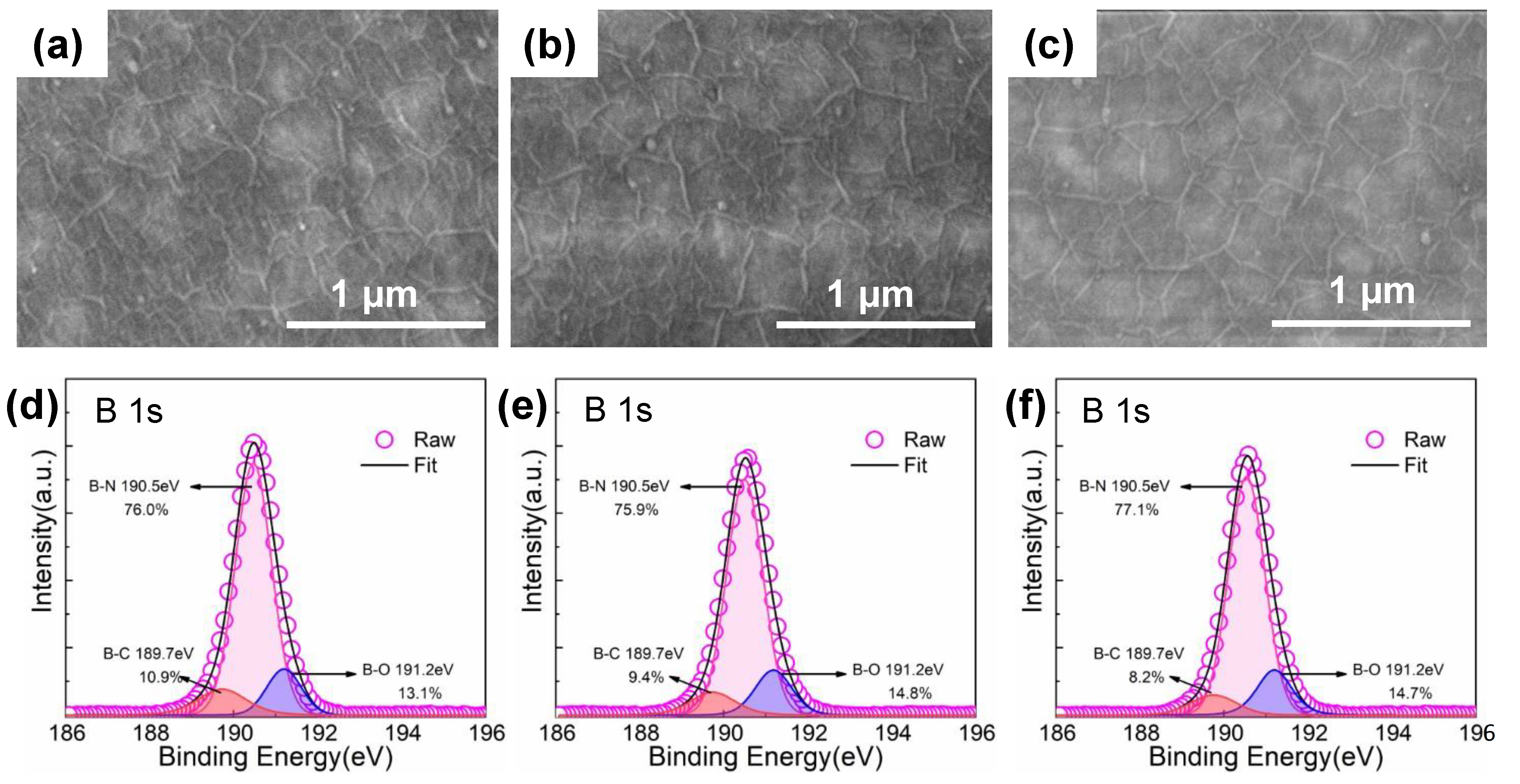
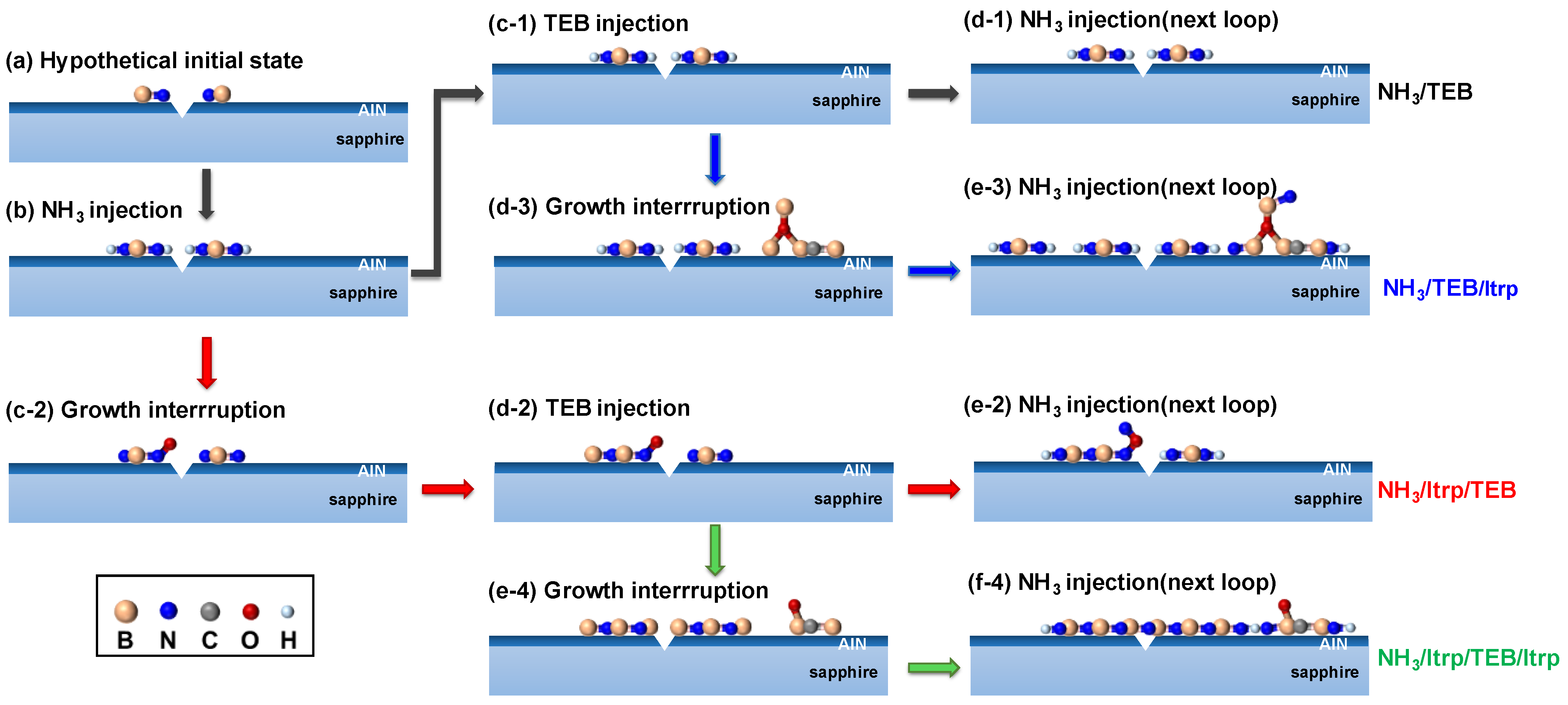
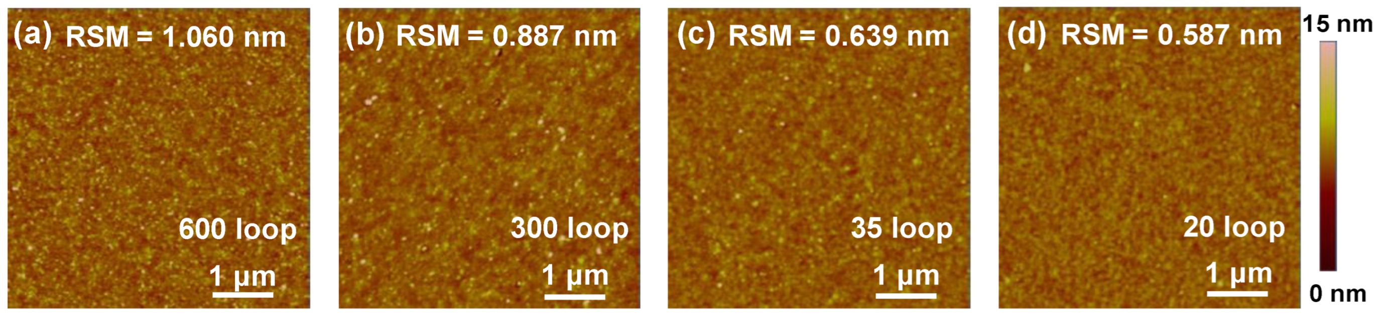
3. Results and Discussion

The variations of h-BN thicknesses with growth loops are summarized in Figure 1e. The surface morphologies under four FME modes are given in Figures S1–S4 (Supplementary Materials). Figure 2 presents the SEM images of h-BN samples grown with fixed 150 loops for intuitive comparisons. For the NH3/TEB mode without any growth interruption, the thickness of h-BN hardly changes with the growth loop. The growth rate is as low as ~0.16 nm/min. Many small black pits exist on the surface, which result from the H2 etching of the sapphire substrate [26]. White BN flakes mainly nucleate around the pits. A similar situation is found in the NH3/Itrp/TEB mode, but the growth rate slightly increases to 0.26 nm/min. As shown in Figure 2a,b, the pit densities are estimated to be 1.89 × 109 cm2 and 1.81 × 109 cm2 respectively for NH3/TEB and NH3/Itrp/TEB modes. The similar pit densities imply that h-BN films are too thin to entirely cover the surfaces of sapphire substrates. When introducing a growth interruption after the TEB injection, the BN thickness increases significantly with prolonged growth loops. The growth rates are calculated to be ~2.74 nm/min and 4.76 nm/min for samples grown in NH3/TEB/Itrp and NH3/Itrp/TEB/Itrp modes, respectively. The clear honeycomb wrinkled surface topographies indicate h-BN growth. The wrinkles are formed due to the thermal compression energy release of h-BN during the cooling process [20]. For the h-BN sample with the NH3/TEB/Itrp mode, lots of 3D BN islands appear on the wrinkles, which should be attributed to the parasitic gas phase reactions [26]. The islands get larger and become the dominant morphological features with increased growth loops, implying a 3D disordered growth. When introducing growth interruptions simultaneously after the NH3 and TEB injections (with the NH3/Itrp/TEB/Itrp mode), the average size and the density of 3D islands decrease notably compared to those with the NH3/TEB/Itrp mode. Therefore, we speculate the interruption after the TEB injection could enhance the surface migration of B adatoms, while the interruption after the NH3 injection could further reduce the parasitic gas phase reactions between precursors and improve the growth rate.
The wrinkle wavelength is usually adopted to describe the size of wrinkled domains, which is estimated by measuring the average length of two crossed line segments across each domain as shown in Figure 2c,d [31]. The BN film with 150 growth loops in the NH3/TEB/Itrp mode has a wrinkle wavelength of 153 nm. As for h-BN grown with 150 growth loops in the NH3/Itrp/TEB/Itrp mode, the wrinkle wavelength increases to 273 nm. As the growth loop (i.e., the film thickness) increases, the wrinkle wavelength monotonically increases, and the density of islands remains at a low level. The results imply that h-BN with the NH3/Itrp/TEB/Itrp mode grows in a layer-by-layer fashion.
The bonding patterns of B and N atoms were investigated by FTIR. As depicted in Figure 3a, the FTIR spectrums of all samples with fixed 150 growth loops have obvious reflection peaks around 1372 cm−1, which is corresponding to the in-plane B-N transverse optical modes (E1u mode) of the sp2-bonded h-BN [32]. Weak reflection peaks locating at 1243 cm−1 are also observed, which are contributed by the C–N bonds [33]. The unintentional incorporation of carbon might occur during the growth process and/or the inevitable surface absorption during the FTIR measurement. Figure 3b shows the XRD 2θ-ω scanning curves to analyze the structural properties of h-BN films. There are no obvious BN-related diffraction peaks in the films with NH3/TEB and NH3/Itrp/TEB growth modes because the BN films are too thin. For samples grown in NH3/TEB/Itrp and NH3/Itrp/TEB/Itrp modes, the (002)-plane diffraction peaks of h-BN are at 25.97° (with a FWHM of 1.6°) and 26.15° (with a FWHM of 1.4°), respectively. The corresponding c-lattice constants are estimated to be 6.86 Å and 6.80 Å, respectively. The deviation from the reported value of bulk h-BN (6.66 Å) may be attributed to weakly ordered turbostratic BN inclusions [34]. The h-BN film grown in the NH3/Itrp/TEB/Itrp mode has a smaller FWHM value and c-lattice constant closer to that of the bulk crystal, demonstrating that further introducing an interruption after the NH3 injection can enhance the phase purity. Besides, a broad and weak diffraction peak around 36.0° is found in four samples, which should be derived from the (002)-plane w-AlN formed during the nitridation of sapphire substrates [35].
The surface chemical states of h-BN under different modes were investigated using XPS. High-resolution scans were performed on peaks of B-1s, N-1s, O-1s, C-1s and Al-2p. All peaks were peak-differentiated and imitated using a linear combination of Gaussian and Lorentzian line shapes, commonly referred as Pearson VII function. Results are shown in Figure 4 and Figures S5 and S6. The main peaks at a binding energy around 190.6 eV for the B 1s and 398.2 eV for the N 1s are in good agreement with the reported values of B-N bonding [35,36]. In Figure 4c,d, sp3 B-O [37] and sp2 B-C [38] bonds are found in the samples with a growth interruption after TEB injection. During the growth process, TEB is first decomposed into solid B and C atoms [39,40], followed by reaction with NH3 to form sp2-BN and CH4. The growth interruption after the TEB injection might result in insufficient supply of NH3, which hiders the second half of the reaction. Therefore, the C impurity is incorporated as sp2-BC [39,41,42,43]. The oxygen impurity should come from the degradation of sapphire substrates at high temperature [44]. Neither sp3 B-O and sp3 N-O bond are observed in the sample without any interruption. It is attributed to the severe passivation of N-terminal growth front and the rapid migration rate of O atoms. The integral intensity of B-O bond in Figure 4c is relatively higher in the h-BN film with the NH3/TEB/Itrp mode, while the integral intensities of B-C bond in Figure 4d and C-B bond in Figure 4l are higher in the h-BN film with the NH3/Itrp/TEB/Itrp mode. This is because the faster growth rate in the NH3/Itrp/TEB/Itrp mode leads to more C impurities incorporated into the film. The B/N atomic ratios of h-BN films under NH3/TEB/Itrp and NH3/Itrp/TEB/Itrp modes are estimated to be 1.41 and 1.45 respectively, indicating of B-rich growth environment. The B/N atomic ratios of h-BN films under NH3/TEB and NH3/Itrp/TEB modes are 0.95 and 1.02 respectively, meaning that the films have a good stoichiometric ratio. In addition, strong N-Al [45] bonds observed in Figure 4e,f, which are consistent with the XRD scanning results. As the thickness of h-BN increases, the surface N-Al bond becomes invisible in Figure 4g,h. The Sp3 N-O bond located at 400.1 eV [46] is found in h-BN film grown in the NH3/Itrp/TEB mode in Figure 4f. With the assistance of sp3 N-O bonds, h-BN debris particles are more likely to formed in the NH3/Itrp/TEB mode compared to that in the NH3/TEB mode in Figures S1 and S2.
The optical properties of h-BN films grown under four FME modes were evaluated by the UV-VIS transmission spectra as shown in Figure 5a. The exact optical bandgap energy (Eg) of h-BN is estimated from the Tauc’s plot in the inset of Figure 5a. The Eg values are 5.88, 5.85, 5.83 and 5.79 eV, respectively, for the NH3/TEB, NH3/Itrp/TEB, NH3/TEB/Itrp, and NH3/Itrp/TEB/Itrp modes. According to previous reports [20,26], the energy bandgap should correspond to the free exciton transition. The h-BN film with the NH3/Itrp/TEB/Itrp mode has the smallest Eg value, indicating of highest defect concentration. There is also an obvious valley in the transmission spectrum at ~300 nm (4.1 eV) of this sample, which is attributed to the transition from CN to VN.
The normalized RT-PL spectra of four sample were displayed to characterize the defect luminescence by dividing the PL intensity by the film thickness. In Figure 5b, the samples under the NH3/TEB/Itrp and NH3/Itrp/TEB/Itrp modes show broad luminescence bands from 3.5 to 2.0 eV. There are two intensive peaks near 3.40 and 3.07 eV, which are probably concerned with the donor-acceptor pair (DAP) recombination involving a shallow ON donor and a deep CN acceptor [47]. The peak at 3.40 eV corresponds to the zero-phonon line (ZPL) of (CN-ON)-complex. The wide asymmetric emission band around 3.07 eV is associated with transitions of phonon-assisted (CN-ON)-complex [48,49,50]. The transition from CN to the valence band with an energy of 2.3 eV might also submerge in the broad luminescence spectra. The defect luminescence intensities in h-BN films with the NH3/TEB/Itrp and NH3/Itrp/TEB/Itrp growth modes are stronger than those with the NH3/TEB and NH3/Itrp/TEB modes. There are two reasons responsible for this phenomenon: (1) the B-rich growth conditions lower the formation energy of CN and ON defects [51,52] and result in high-concentration defects; (2) the rapid growth rates facilitate the incorporation of impurities.
Considering the B-rich growth environment and high concentration impurities in the NH3/Itrp/TEB/Itrp mode, a series of experiments were carried out to study the effect of the duration of NH3 supply. As shown in Figure 6a–c, the surface morphology is nearly identical as the NH3 injection duration increases from 2 s to 12 s. The thickness decreases from 29 nm to 25 nm, and the corresponding growth rate decreases from 5.78 nm/min to 5.02 nm/min. It should be noted that the growth rates are somehow higher than that of the above experiments because of the state fluctuations of facilities at different stages. Furthermore, the ratios of the B-C (B-O) bond to the B 1s peak are 10.9% (13.1%), 9.4% (14.8%), and 8.2% (14.7%) for samples with NH3 injection durations of 2 s, 4 s and 12 s, respectively, and the B/N atomic ratios are estimated to be around 1.46~1.43. It seems that the increase of NH3 injection duration in each loop could suppress the incorporation of C impurity, whereas increase the incorporation probability of O impurity; the growth rate would be slightly decreased due to the reduced surface migration of B adatoms [27] and the aggravated passivation of N-terminal growth front. More careful optimization of growth conditions under NH3/Itrp/TEB/Itrp mode are needed to inhibit the concomitant incorporation of C and O impurities, which are beyond the scope of this work.
Based on the morphological and chemical states analysis, the growth mechanisms of h-BN under four FME modes are discussed as below. As shown in Figure 7, in the early stage of the growth, BN nucleates primarily around the H2 etching caused pits on the nitrided substrate surface. In the absence of growth interruptions, the growth rate is quite slow due to the passivation of N-terminal growth fronts by hydrogen atoms [53], and the low surface mobility of B adatoms. Introducing the growth interruption after NH3 injection could remove the passivation of N-terminal fronts, while introducing the growth interruption after TEB injection could enhance the migration of B adatoms. Considering the huge difference in the growth rates between the samples under NH3/Itrp/TEB and NH3/TEB/Itrp modes, we can conclude that the growth rate is dominantly determined by the surface migration ability of B adatoms. Adopting growth interruptions after NH3 and TEB injections would suppress the possible the parasitic reaction more thoroughly, further increases the growth rate and improves the surface morphology. In addition, the high growth rate leads to the incorporation of C and O impurities to substitute N sites, forming sp2 B-C bonds and sp3 B-O bonds.
Finally, h-BN films with a similar thickness (2 ± 0.3 nm) were prepared using different FME methods with 4 s NH3 injection durations by adjusting the growth loops. Figure 8 shows the surface morphology of h-BN films grown by four FME methods. The surface roughness decreases after introducing the growth interruption. The sample using the NH3/Itrp/TEB/Itrp growth mode has the smoothest surface because of the enhanced surface mobility of B adatoms and weakened parasitic reaction.
In Figure 9a,c, the characteristic peaks of h-BN are significant in FTIR and Raman spectra for all samples. The sapphire substrate has a characteristic peak at 1353.8 cm−1 (marked as peak1) in Figure 9c. It might interfere the observation of the characteristic peak of thin h-BN, which is around 1370 cm−1 contributed by the E2g vibration mode [54]. Hence, we used multi-peaks gaussian fitting to obtain the calibrated FWHM values and the Raman shifts of h-BN. The fitted FWHM values of fixed peak1 is around 37 cm−1 for all samples, confirming that the fitting results are reliable. The h-BN sample under NH3/Itrp/TEB FME mode has the narrowest FWHM values of characteristic FTIR and Raman peaks, 26 cm−1 and 23 cm−1, respectively, indicating that h-BN with excellent crystalline quality can be achieved by solely introducing an interruption after the NH3 injection. The passivation of the N-terminals can be efficiently eliminated during the interruption, thus promote the lateral merging of nucleation islands, and improve the crystallinity of h-BN. On the other hand, the relative slow growth rate reduces the concentration of N-related defects.

4. Conclusions

In summary, the effect of the growth interruption on the surface morphology and crystalline quality of h-BN by MOCVD was investigated. It was found that the growth interruption after the TEB injection could enhance the surface mobility of B adatoms and improve the growth rate of h-BN dramatically; while the growth interruption after the NH3 injection could eliminate the N-terminal passivation and reduce the parasitic reactions between precursors. As a result, the h-BN film grown in the NH3/Itrp/TEB/Itrp mode presents the smoothest surface morphology and the fastest growth rate, providing a feasible method to prepare thick h-BN films. The surface RMS of 24 nm-thick h-BN film is 2.01 nm after the 150-loop NH3/Itrp/TEB/Itrp growth mode, which is lower than that of 20 nm-thick reported in [26] (RMS = 3.77 nm). But further optimization of growth conditions is required to suppress the concomitant incorporation of C and O impurities. Meanwhile, thin h-BN with excellent crystalline quality can be obtained by introducing a growth interruption solely after the NH3 injection due to the promotion of the lateral growth of BN domains and the low concentration of defects. Under this mode, the FWHM values of E2g peaks of 2 nm-thick h-BN is 23 cm−1, which is compatible to the results in [26,29,30] (27–36 cm−1).

Supplementary Materials

The following supporting information can be downloaded at https://www.mdpi.com/article/10.3390/cryst13030486/s1. Figure S1: The surface morphology variations of h-BN films grown by NH3/TEB with the growth loops; Figure S2: The surface morphology variations of h-BN films grown by NH3/Itrp/TEB with the growth loops; Figure S3: The surface morphology variations of h-BN films grown by NH3/TEB/Itrp with the growth loops; Figure S4: The surface morphology variations of h-BN films grown by NH3/Itrp/TEB/Itrp with the growth loops; Figure S5: The XPS spectra of Al 2p peak in h-BN film under four FME modes. (a) NH3/TEB, (b) NH3/Itrp/TEB, (c) NH3/TEB/Itrp, (d) NH3/Itrp/TEB/Itrp; Figure S6: The XPS spectra of O 1s peak in h-BN film under four FME modes. (a) NH3/TEB, (b) NH3/Itrp/TEB, (c) NH3/TEB/Itrp, (d) NH3/Itrp/TEB/Itrp; Table S1: The variations of binding energy, FWHM and percentage content of different bonds of B 1s, N 1s and C 1s XPS core level spectra in h-BN films by four FME modes.

Author Contributions

Conceptualization, Q.Z. and Y.G.; methodology, Q.Z., Y.G. and Z.L.; validation, Q.Z. and Y.G.; formal analysis, Q.Z., Y.G., D.W. and Q.L.; investigation, Q.Z. and D.W.; resources, Q.Z. and D.W.; data curation, Q.Z.; writing—original draft preparation, Q.Z.; writing—review and editing, Q.Z., Y.G., Z.L., D.W. and Q.L.; visualization, Q.Z.; supervision, J.Y., J.L. and J.W.; project administration, J.Y., J.L. and J.W.; funding acquisition, Y.G., J.Y. and J.W. All authors have read and agreed to the published version of the manuscript.

Funding

This work was supported by National Key RD Program of China (2022YFB3605104 and 2016YFB0400800); National Natural Science Foundation of China (62135013, 62022080, 62274163, 62234001); Youth Innovation Promotion Association CAS (2022000028 and 2023123).

Institutional Review Board Statement

Not applicable.

Informed Consent Statement

Not applicable.

Data Availability Statement

The data presented in this study are available on request from the corresponding author.

Conflicts of Interest

The authors declare no conflict of interest.

References

  1. Liu, L.; Feng, Y.P.; Shen, Z.X. Structural and electronic properties ofh-BN. Phys. Rev. B 2003, 68, 104102. [Google Scholar] [CrossRef]
  2. Ooi, N.; Rairkar, A.; Lindsley, L.; Adams, J.B. Electronic structure and bonding in hexagonal boron nitride. J. Phys. Condens. Matter 2006, 18, 97–115. [Google Scholar] [CrossRef]
  3. Hod, O. Graphite and Hexagonal Boron-Nitride have the Same Interlayer Distance. Why? J. Chem. Theory Comput. 2012, 8, 1360–1369. [Google Scholar] [CrossRef] [Green Version]
  4. Han, N.; Liu, H.; Zhang, J.; Gao, J.; Zhao, J. Atomistic understanding of the lateral growth of graphene from the edge of an h-BN domain: Towards a sharp in-plane junction. Nanoscale 2017, 9, 3585–3592. [Google Scholar] [CrossRef]
  5. Ludwiczak, K.; Da Browska, A.K.; Binder, J.; Tokarczyk, M.; Iwanski, J.; Kurowska, B.; Turczynski, J.; Kowalski, G.; Bozek, R.; Stepniewski, R.; et al. Heteroepitaxial Growth of High Optical Quality, Wafer-Scale van der Waals Heterostrucutres. ACS Appl. Mater. Interfaces 2021, 13, 47904–47911. [Google Scholar] [CrossRef]
  6. Levendorf, M.P.; Kim, C.J.; Brown, L.; Huang, P.Y.; Havener, R.W.; Muller, D.A.; Park, J. Graphene and boron nitride lateral heterostructures for atomically thin circuitry. Nature 2012, 488, 627–632. [Google Scholar] [CrossRef]
  7. Wang, H.; Zhao, Y.; Xie, Y.; Ma, X.; Zhang, X. Recent progress in synthesis of two-dimensional hexagonal boron nitride. J. Semicond. 2017, 38, 031003. [Google Scholar] [CrossRef]
  8. Kubota, Y.; Watanabe, K.; Tsuda, O.; Taniguchi, T. Deep ultraviolet light-emitting hexagonal boron nitride synthesized at atmospheric pressure. Science 2007, 317, 932–934. [Google Scholar] [CrossRef] [PubMed] [Green Version]
  9. Cassabois, G.; Valvin, P.; Gil, B. Hexagonal boron nitride is an indirect bandgap semiconductor. Nat. Photonics 2016, 10, 262–266. [Google Scholar] [CrossRef] [Green Version]
  10. Wang, P.; Lee, W.; Corbett, J.P.; Koll, W.H.; Vu, N.M.; Laleyan, D.A.; Wen, Q.; Wu, Y.; Pandey, A.; Gim, J.; et al. Scalable Synthesis of Monolayer Hexagonal Boron Nitride on Graphene with Giant Bandgap Renormalization. Adv. Mater. 2022, 34, e2201387. [Google Scholar] [CrossRef]
  11. Li, Q.; Zhang, Q.; Bai, Y.; Zhang, H.; Hu, P.; Li, Y.; Yun, F. Deep-UV hexagonal boron nitride (hBN)/BAlN distributed Bragg reflectors fabricated by RF-sputtering. Opt. Mater. Express 2020, 11, 180–188. [Google Scholar] [CrossRef]
  12. Laleyan, D.A.; Zhao, S.R.; Woo, S.Y.; Tran, H.N.; Le, H.B.; Szkopek, T.; Guo, H.; Botton, G.A.; Mi, Z.T. AIN/h-BN Heterostructures for Mg Dopant-Free Deep Ultraviolet Photonics. Nano Lett. 2017, 17, 3738–3743. [Google Scholar] [CrossRef] [PubMed]
  13. Wu, Q.; Guo, Y.; Sundaram, S.; Yan, J.; Zhang, L.; Wei, T.; Wei, X.; Wang, J.; Ougazzaden, A.; Li, J. Exfoliation of AlN film using two-dimensional multilayer hexagonal BN for deep-ultraviolet light-emitting diodes. Appl. Phys. Express 2019, 12, 015505. [Google Scholar] [CrossRef]
  14. Chen, J.; Wang, G.; Meng, J.; Cheng, Y.; Yin, Z.; Tian, Y.; Huang, J.; Zhang, S.; Wu, J.; Zhang, X. Low-Temperature Direct Growth of Few-Layer Hexagonal Boron Nitride on Catalyst-Free Sapphire Substrates. ACS Appl. Mater. Interfaces 2022, 14, 7004–7011. [Google Scholar] [CrossRef]
  15. Grenadier, S.; Maity, A.; Li, J.; Lin, J.Y.; Jiang, H.X. Lateral charge carrier transport properties of B-10 enriched hexagonal BN thick epilayers. Appl. Phys. Lett. 2019, 115, 072108. [Google Scholar] [CrossRef]
  16. Li, J.; Majety, S.; Dahal, R.; Zhao, W.P.; Lin, J.Y.; Jiang, H.X. Dielectric strength, optical absorption, and deep ultraviolet detectors of hexagonal boron nitride epilayers. Appl. Phys. Lett. 2012, 101, 171112. [Google Scholar] [CrossRef] [Green Version]
  17. Bourrellier, R.; Meuret, S.; Tararan, A.; Stephan, O.; Kociak, M.; Tizei, L.H.; Zobelli, A. Bright UV Single Photon Emission at Point Defects in h-BN. Nano Lett. 2016, 16, 4317–4321. [Google Scholar] [CrossRef]
  18. Gan, L.; Zhang, D.; Zhang, R.; Zhang, Q.; Sun, H.; Li, Y.; Ning, C.Z. Large-Scale, High-Yield Laser Fabrication of Bright and Pure Single-Photon Emitters at Room Temperature in Hexagonal Boron Nitride. ACS Nano 2022, 16, 14254–14261. [Google Scholar] [CrossRef]
  19. Li, Q.; Wang, M.; Bai, Y.; Zhang, Q.; Zhang, H.; Tian, Z.; Guo, Y.; Zhu, J.; Liu, Y.; Yun, F.; et al. Two-Inch Wafer-Scale Exfoliation of Hexagonal Boron Nitride Films Fabricated by RF-Sputtering. Adv. Funct. Mater. 2022, 32, 2206094. [Google Scholar] [CrossRef]
  20. Li, X.; Sundaram, S.; El Gmili, Y.; Ayari, T.; Puybaret, R.; Patriarche, G.; Voss, P.L.; Salvestrini, J.P.; Ougazzaden, A. Large-Area Two-Dimensional Layered Hexagonal Boron Nitride Grown on Sapphire by Metalorganic Vapor Phase Epitaxy. Cryst. Growth Des. 2016, 16, 3409–3415. [Google Scholar] [CrossRef]
  21. Dahal, R.; Li, J.; Majety, S.; Pantha, B.N.; Cao, X.K.; Lin, J.Y.; Jiang, H.X. Epitaxially grown semiconducting hexagonal boron nitride as a deep ultraviolet photonic material. Appl. Phys. Lett. 2011, 98, 211110. [Google Scholar] [CrossRef] [Green Version]
  22. Doan, T.C.; Li, J.; Lin, J.Y.; Jiang, H.X. Charge carrier transport properties in layer structured hexagonal boron nitride. AIP Adv. 2014, 4, 107126. [Google Scholar] [CrossRef] [Green Version]
  23. Paduano, Q.S.; Snure, M.; Bondy, J.; Zens, T.W.C. Self-terminating growth in hexagonal boron nitride by metal organic chemical vapor deposition. Appl. Phys. Express 2014, 7, 071004. [Google Scholar] [CrossRef]
  24. Rice, A.; Allerman, A.; Crawford, M.; Beechem, T.; Ohta, T.; Spataru, C.; Figiel, J.; Smith, M. Effects of deposition temperature and ammonia flow on metal-organic chemical vapor deposition of hexagonal boron nitride. J. Cryst. Growth 2018, 485, 90–95. [Google Scholar] [CrossRef]
  25. Kobayashi, Y.; Makimoto, T. Growth of Boron Nitride on 6H–SiC Substrate by Flow-Rate Modulation Epitaxy. Jpn. J. Appl. Phys. 2006, 45, 3519–3521. [Google Scholar] [CrossRef]
  26. Chugh, D.; Wong-Leung, J.; Li, L.; Lysevych, M.; Tan, H.H.; Jagadish, C. Flow modulation epitaxy of hexagonal boron nitride. 2D Mater. 2018, 5, 045018. [Google Scholar] [CrossRef]
  27. Yang, X.; Nitta, S.; Nagamatsu, K.; Bae, S.-Y.; Lee, H.-J.; Liu, Y.; Pristovsek, M.; Honda, Y.; Amano, H. Growth of hexagonal boron nitride on sapphire substrate by pulsed-mode metalorganic vapor phase epitaxy. J. Cryst. Growth 2018, 482, 1–8. [Google Scholar] [CrossRef]
  28. Jiang, H.X.; Lin, J.Y. Review—Hexagonal Boron Nitride Epilayers: Growth, Optical Properties and Device Applications. ECS J. Solid State Sci. Technol. 2016, 6, Q3012–Q3021. [Google Scholar] [CrossRef]
  29. Kim, D.Y.; Han, N.; Jeong, H.; Kim, J.; Hwang, S.; Kim, J.K. Role of hydrogen carrier gas on the growth of few layer hexagonal boron nitrides by metal-organic chemical vapor deposition. AIP Adv. 2017, 7, 045116. [Google Scholar] [CrossRef] [Green Version]
  30. Kim, D.Y.; Han, N.; Jeong, H.; Kim, J.; Hwang, S.; Song, K.; Choi, S.-Y.; Kim, J.K. Pressure-Dependent Growth of Wafer-Scale Few-layer h-BN by Metal–Organic Chemical Vapor Deposition. Cryst. Growth Des. 2017, 17, 2569–2575. [Google Scholar] [CrossRef]
  31. Bera, K.; Chugh, D.; Patra, A.; Tan, H.H.; Jagadish, C.; Roy, A. Strain distribution in wrinkled hBN films. Solid State Commun. 2020, 310, 113847. [Google Scholar] [CrossRef]
  32. Geick, R.; Perry, C.H.; Rupprecht, G. Normal Modes in Hexagonal Boron Nitride. Phys. Rev. 1966, 146, 543–547. [Google Scholar] [CrossRef]
  33. Yap, Y.K.; Kida, S.; Aoyama, T.; Mori, Y.; Sasaki, T. Influence of negative dc bias voltage on structural transformation of carbon nitride at 600 degrees C. Appl. Phys. Lett. 1998, 73, 915–917. [Google Scholar] [CrossRef]
  34. Kobayashi, Y.; Akasaka, T. Hexagonal BN epitaxial growth on (0001) sapphire substrate by MOVPE. J. Cryst. Growth 2008, 310, 5044–5047. [Google Scholar] [CrossRef]
  35. Ahmed, K.; Dahal, R.; Weltz, A.; Lu, J.J.Q.; Danon, Y.; Bhat, I.B. Effects of sapphire nitridation and growth temperature on the epitaxial growth of hexagonal boron nitride on sapphire. Mater. Res. Express 2017, 4, 015007. [Google Scholar] [CrossRef] [Green Version]
  36. Tay, R.Y.; Tsang, S.H.; Loeblein, M.; Chow, W.L.; Loh, G.C.; Toh, J.W.; Ang, S.L.; Teo, E.H.T. Direct growth of nanocrystalline hexagonal boron nitride films on dielectric substrates. Appl. Phys. Lett. 2015, 106, 101901. [Google Scholar] [CrossRef]
  37. Souqui, L.; Palisaitis, J.; Högberg, H.; Pedersen, H. Plasma CVD of B–C–N thin films using triethylboron in argon–nitrogen plasma. J. Mater. Chem. C 2020, 8, 4112–4123. [Google Scholar] [CrossRef] [Green Version]
  38. Nasrin, K.; Sudharshan, V.; Subramani, K.; Karnan, M.; Sathish, M. In-Situ Synergistic 2D/2D MXene/BCN Heterostructure for Superlative Energy Density Supercapacitor with Super-Long Life. Small 2022, 18, e2106051. [Google Scholar] [CrossRef] [PubMed]
  39. Lewis, J.S.; Vaidyaraman, S.; Lackey, W.J.; Agrawal, P.K.; Freeman, G.B.; Barefield, E.K. Chemical vapor deposition of boron-carbon films using organometallic reagents. Mater. Lett. 1996, 27, 327–332. [Google Scholar] [CrossRef]
  40. Mazaheri, A.; Javadi, M.; Abdi, Y. Chemical Vapor Deposition of Two-Dimensional Boron Sheets by Thermal Decomposition of Diborane. ACS Appl. Mater. Interfaces 2021, 13, 8844–8850. [Google Scholar] [CrossRef]
  41. Snure, M.; Paduano, Q.; Hamilton, M.; Shoaf, J.; Mann, J.M. Optical characterization of nanocrystalline boron nitride thin films grown by atomic layer deposition. Thin Solid Film. 2014, 571, 51–55. [Google Scholar] [CrossRef]
  42. Caban, P.A.; Teklinska, D.; Michalowski, P.P.; Gaca, J.; Wojcik, M.; Grzonka, J.; Ciepielewski, P.; Mozdzonek, M.; Baranowski, J.M. The role of hydrogen in carbon incorporation and surface roughness of MOCVD-grown thin boron nitride. J. Cryst. Growth 2018, 498, 71–76. [Google Scholar] [CrossRef]
  43. Pedersen, H.; Höglund, C.; Birch, J.; Jensen, J.; Henry, A. Low Temperature CVD of Thin, Amorphous Boron-Carbon Films for Neutron Detectors. Chem. Vap. Depos. 2012, 18, 221–224. [Google Scholar] [CrossRef] [Green Version]
  44. Yang, X.; Nitta, S.; Pristovsek, M.; Liu, Y.; Nagamatsu, K.; Kushimoto, M.; Honda, Y.; Amano, H. Interface amorphization in hexagonal boron nitride films on sapphire substrate grown by metalorganic vapor phase epitaxy. Appl. Phys. Express 2018, 11, 051002. [Google Scholar] [CrossRef]
  45. Zhao, L.; Yang, K.; Ai, Y.; Zhang, L.; Niu, X.; Lv, H.; Zhang, Y. Crystal quality improvement of sputtered AlN film on sapphire substrate by high-temperature annealing. J. Mater. Sci. Mater. Electron. 2018, 29, 13766–13773. [Google Scholar] [CrossRef]
  46. Thangasamy, P.; Santhanam, M.; Sathish, M. Supercritical Fluid Facilitated Disintegration of Hexagonal Boron Nitride Nanosheets to Quantum Dots and Its Application in Cells Imaging. ACS Appl. Mater. Interfaces 2016, 8, 18647–18651. [Google Scholar] [CrossRef]
  47. Du, X.Z.; Li, J.; Lin, J.Y.; Jiang, H.X. The origin of deep-level impurity transitions in hexagonal boron nitride. Appl. Phys. Lett. 2015, 106, 021110. [Google Scholar] [CrossRef] [Green Version]
  48. Berzina, B.; Korsaks, V.; Trinkler, L.; Sarakovskis, A.; Grube, J.; Bellucci, S. Defect-induced blue luminescence of hexagonal boron nitride. Diam. Relat. Mater. 2016, 68, 131–137. [Google Scholar] [CrossRef]
  49. Vokhmintsev, A.; Weinstein, I.; Zamyatin, D. Electron-phonon interactions in subband excited photoluminescence of hexagonal boron nitride. J. Lumin. 2019, 208, 363–370. [Google Scholar] [CrossRef]
  50. Sunny, A.; Balapure, A.; Ganesan, R.; Thamankar, R. Room-Temperature Deep-UV Photoluminescence from Low-Dimensional Hexagonal Boron Nitride Prepared Using a Facile Synthesis. ACS Omega 2022, 7, 33926–33933. [Google Scholar] [CrossRef]
  51. Ngwenya, T.B.; Ukpong, A.M.; Chetty, N. Defect states of complexes involving a vacancy on the boron site in boronitrene. Phys. Rev. B 2011, 84, 245425. [Google Scholar] [CrossRef] [Green Version]
  52. Weston, L.; Wickramaratne, D.; Mackoit, M.; Alkauskas, A.; Van de Walle, C.G. Native point defects and impurities in hexagonal boron nitride. Phys. Rev. B 2018, 97, 214104. [Google Scholar] [CrossRef] [Green Version]
  53. He, Y.; Tian, H.; Khanaki, A.; Shi, W.; Tran, J.; Cui, Z.; Wei, P.; Liu, J. Large-area adlayer-free single-layer h-BN film achieved by controlling intercalation growth. Appl. Surf. Sci. 2019, 498, 143851. [Google Scholar] [CrossRef]
  54. Cao, X.K.; Clubine, B.; Edgar, J.H.; Lin, J.Y.; Jiang, H.X. Two-dimensional excitons in three-dimensional hexagonal boron nitride. Appl. Phys. Lett. 2013, 103, 191106. [Google Scholar] [CrossRef]
Figure 1. The schematic diagrams of (a) NH3/TEB, (b) NH3/Itrp/TEB, (c) NH3/TEB/Itrp and (d) NH3/Itrp/TEB/Itrp. (e) the thickness variations of h-BN thickness with growth loops under four FME modes.
Crystals 13 00486 g001
Figure 2. The SEM images of BN films with fixed 150 growth loops under four FME modes: (a) NH3/TEB, (b) NH3/Itrp/TEB, (c) NH3/TEB/Itrp, (d) NH3/Itrp/TEB/Itrp. White crossed line segments within wrinkled domains in (c,d) are used to estimate the wrinkle wavelength.
Crystals 13 00486 g002
Figure 3. (a) FTIR spectra and (b) XRD 2theta-omega scans of the h-BN films with fixed 150 growth loops under four FME modes. The inset is magnified spectra in the red circle in (a).
Crystals 13 00486 g003
Figure 4. The XPS spectra of (ad) B-1s, (eh) N-1s and (il) C-1s in h-BN film under four FME modes. (a,e,i) NH3/TEB, (b,f,j) NH3/Itrp/TEB, (c,g,k) NH3/TEB/Itrp, (d,h,l) NH3/Itrp/TEB/Itrp.
Crystals 13 00486 g004
Figure 5. (a) The UV–vis transmission spectra and (b) normalized RT-PL spectra of the h-BN films with fixed 150 growth loops under four FME modes. The inset of (a) shows the (αhν)2 versus photon energy hν for determining the optical bandgap energy of h-BN.
Crystals 13 00486 g005
Figure 6. The SEM images and XPS spectra of h-BN films with different NH3 injection durations under NH3/Itrp/TEB/Itrp modes: (a,d) 2 s, (b,e) 4 s and (c,f) 12 s. The TEB injection duration and the growth loop were kept 2 s and 150, respectively.
Crystals 13 00486 g006
Figure 7. Schematic growth model of h-BN grown by NH3/TEB (a,b,c-1,d-1), NH3/Itrp/TEB (a,b,c-2,d-2,e-2), NH3/Itrp/TEB (a,b,c-1,d-3,e-3) and NH3/Itrp/TEB/Itrp (a,b,c-2,d-2,e-4,f-4).
Crystals 13 00486 g007
Figure 8. The AFM images of 2-nm-thick BN films grown by four FME modes: (a) NH3/TEB, (b) NH3/Itrp/TEB, (c) NH3/TEB/Itrp, (d) NH3/Itrp/TEB/Itrp.
Crystals 13 00486 g008
Figure 9. (a) FTIR spectra, (b) the variations of FWHM of Eu1 peaks, (c) Raman spectra and (d) the variations of FWHM (left axis in black) and location of E2g (right axis in red) of the h-BN with a similar thickness grown by four FME modes.
Crystals 13 00486 g009
Disclaimer/Publisher’s Note: The statements, opinions and data contained in all publications are solely those of the individual author(s) and contributor(s) and not of MDPI and/or the editor(s). MDPI and/or the editor(s) disclaim responsibility for any injury to people or property resulting from any ideas, methods, instructions or products referred to in the content.

