Article

Mechanochemically Synthesized Chalcogenide Cu3BiS3 Nanocrystals in an Environmentally Friendly Manner for Solar Cell Applications

by
Erika Dutková
1,*,
Matej Baláž
1,
María Jesús Sayagués
2,
Jaroslav Kováč
3 and
Jaroslav Kováč, Jr.
3
1
Department of Mechanochemistry, Institute of Geotechnics Slovak Academy of Sciences, Watsonova 45, 04001 Košice, Slovakia
2
Institute of Material Science of Seville, Consejo Superior de Investigaciones Científicas, Seville University, Avenida Américo Vespucio 49, 41092 Seville, Spain
3
Institute of Electronics and Photonics, Slovak University of Technology, Ilkovičova 3, 81219 Bratislava, Slovakia
*
Author to whom correspondence should be addressed.
Crystals 2023, 13(3), 487; https://doi.org/10.3390/cryst13030487
Submission received: 31 January 2023 / Revised: 3 March 2023 / Accepted: 4 March 2023 / Published: 11 March 2023
(This article belongs to the Special Issue Optoelectronics of Thin Films and Nanoparticles)

Abstract

:
Ternary wittichenite Cu3BiS3 nanocrystals were prepared mechanochemically using a planetary ball mill from elemental copper, bismuth and sulfur in a stoichiometric ratio in only 5 min. The orthorhombic wittichenite Cu3BiS3 was nanocrystalline with an approximate crystallite size of 38 nm ± 9 nm, as confirmed by Rietveld refinement. The nanocrystalline character of orthorhombic Cu3BiS3 was also proven by transmission electron microscopy. The measured Raman spectrum confirmed the formation of pure wittichenite Cu3BiS3. The morphology characterization demonstrated the homogeneity of the sample. The value of the specific surface area for pure mechanochemically prepared Cu3BiS3 after 5 min was 2.7 m2g−1. The optical properties were investigated using UV–Vis absorption and micro-photoluminescence spectroscopy. From the absorption UV–Vis spectrum, the value of the bandgap energy was determined to be 1.52 eV, which creates an assumption for the use of wittichenite Cu3BiS3 in photovoltaic applications. The optoelectrical properties of the prepared Cu3BiS3 nanocrystals were verified by current–voltage measurements in the dark and under white light illumination. The photocurrent increased by 26% compared to the current in the dark at a voltage of 1 V. The achieved results confirmed a very fast and efficient way of synthesizing a ternary wittichenite Cu3BiS3, which can be used for applications in solar cells.

1. Introduction

Ternary copper–bismuth–sulfide (Cu-Bi-S) materials have recently gained importance in solar cell investigation as substitutive absorbers because of their low toxicity, low cost and earth-abundant elements [1].
Wittichenite Cu3BiS3 has a p-type conductivity, direct bandgap (1.10–1.86 eV) and large absorption coefficient (>105 cm1). Furthermore, Bi, compared with Te and In, is less toxic, readily accessible and relatively inexpensive [2]. Cu3BiS3 has been proposed as an potential absorber material for photovoltaics [3] due to the suitable direct optical bandgap, which is close to the optimum value for efficient solar energy conversion [4]. Cu3BiS3 nanomaterials also have potential applications in bio-imaging [5,6].
Wittichenite Cu3BiS3, with many potential applications, has been tentatively synthesized using various techniques. Cu3BiS3 nanorods with strong absorption in the second near-infrared window were successfully synthesized by a facile organic route using oleylamine as the stabilizing agent [7]. Semiconducting Cu3BiS3 thin films produced by the solid-state reaction from chemically deposited CuS and thermally evaporated bismuth thin films were studied in paper [8]. Cu3BiS3 nanorods with different aspect ratios were synthesized via an ethanol–thermal pathway between CuCl2, H2O, BiCl3 and thiourea using different solvents in a previous study [9]. Large-grain and highly crystalline Cu3BiS3 thin films were synthesized by a one-step dimethyl sulfoxide-based solution coating process [10]. One-dimensional Cu3BiS3 nano- and micro-structures prepared by a solvothermal route using the structural directing agent polyethylene glycol as a soft template were investigated in paper [11]. Single tetra-pod-like 3D-architecture Cu3BiS3 nanopowders for photodetector applications were prepared using the solvothermal route by Murali et al. [12]. Yan et al. [13] prepared Cu3BiS3 nanostructures with various morphology through the solvothermal method. Cu3BiS3 dendrites prepared by cyclic microwave radiation using L-cysteine and a complexing agent were investigated by Aup-Ngoen et al. [14]. Zeng et al. [15] prepared flower-like Cu3BiS3 hierarchical structures using the facile hydrothermal method. Coral-shaped Cu3BiS3 nanostructures were synthesized by a rapid polyol process by Shen et al. [16]. Deng et al. [17] synthesized Cu3BiS3 nanosheets and nanoparticles using 1-octadencence and 1-dodecanethiol as capping ligands through a single-source method. Wittichenite Cu3BiS3 nanocrystals, which exhibit a clear photoresponse in I-V measurement, were prepared by the hot-injection method by Yan et al. [18]. Cu3BiS3 nanoparticles synthesized by hydrothermal and solvothermal methods using L-cysteine biomolecules and a complexing agent were studied by Aup-Ngoen et al. [19]. Wittichenite Cu3BiS3 semiconductor thin films deposited on glass slides via a spray pyrolysis approach were investigated by Liu et al. [20]. Zhong et al. [21] synthesized flower-like Cu3BiS3 nanorods using a facile biomolecule-assisted solvothermal method employing CuCl2·2H2O, Bi(NO)3·5H2O and L-cystine as reactants. Cu-Bi-S thin films deposited onto soda lime glass substrates using a one-stage co-evaporation process from Cu2S and Bi2S3 sources were studied by Hussain et al. [22]. Cu3BiS3 films for efficient hydrogen evolution from solar-driven photoelectrochemical water splitting prepared using the spray pyrolysis method were investigated in study [23]. Cu3BiS3 was also prepared by a simplified route through chemical bath deposition in paper [24]. A comprehensive review of the synthesis, characterizations, processing, and solar photovoltaic applications of Cu3BiS3 thin films was reported in paper [2].
Mechanochemistry is a branch of chemistry used for the extensive diversity of synthesis of different organic and inorganic materials [25,26,27]. Currently, its application potential is already exhaustive and new applications regularly appear [28]. By applying the tools of high-energy ball milling, it offers a satisfactory option to prepare nanocrystalline materials in a one-step, solvent-free, environmentally friendly manner without the need to apply external heating or pressure, in contrast to the classical methods [29]. Mechanochemistry is a scalable and reproducible method. Moreover, the mechanochemically synthesized compounds are composed of morphologically inhomogeneous, weakly crystallized and structurally disordered nanoparticles. The mechanochemical solid-state approach has also been successfully applied for ternary chalcogenide synthesis by our group [30,31,32,33,34].
To our best knowledge, the wittichenite Cu3BiS3 preparation by a facile one-step environmentally friendly mechanochemical synthesis is reported for the first time in this study. The main focus is on its optical and optoelectrical properties.

2. Materials and Methods

Ternary Cu3BiS3 nanocrystals were prepared in the planetary ball mill Pulverisette 6 (Fritsch, Idar-Oberstein, Germany) from 1.92 g of copper (99.7%, Merck, Darmstadt, Germany), 2.11 g of bismuth (99.5%, Aldrich, Taufkirchen, Germany) and 0.97 g of sulfur (99%, Ites, Vranov n/T, Slovakia) in a Cu:Bi:S stoichiometric ratio of 3:1:3, according to the reaction (Equation (1)). The particle size distribution of the elemental precursors used for the synthesis is shown in the Supplementary Materials (SM) in Figure S1.
3Cu + Bi + 3S→Cu3BiS3
The mechanochemical synthesis was performed using a tungsten carbide milling chamber (250 mL in volume) filled with 50 tungsten carbide milling balls (10 mm in diameter) at 550 rpm, in an argon atmosphere (>99.998%, Linde Gas group, Bratislava, Slovakia), for 0.5–5 min without break cooling due to the very short milling times. The milling chamber was not filled with Ar using a glow box; instead, Ar gas was purged for about 3 min into the chamber while air was being pushed out of it via the other ventil. A ball-to-powder ratio of 73:1 was used. The yield of mechanochemically synthesized Cu3BiS3 was 96%.
XRD characterization was carried out using a D8 Advance diffractometer (Brucker, Bremen, Germany) with the CuKα radiation in the Bragg–Brentano configuration. The generator was adjusted to 40 kV and 40 mA. The divergence and receiving slits were 0.3° and 0.1 mm, respectively. The XRD patterns were observed in the range of 10–70° 2θ with a step of 0.03°. Rietveld refinements from the XRD data of the synthesized samples were carried out using the TOPAS Academic program [35,36]. For the purpose of obtaining a proper geometry setup and to eliminate instrumental broadening, the instrumental resolution function was identified by the refinement of LaB6 standard specimen. The phase identification was made using the JCPDS PDF2 database [37].
Micro-Raman and micro-PL spectra were recorded by a UV–Vis–NIR confocal Raman microscope (Spectroscopy & Imaging, Warstein, Germany). An Ar laser with a wavelength of 514 nm was used to excite the measured sample.
The microstructural characterization was investigated using a TEM-200 kV JEOL-2100-PLUS microscope (JEOL, Akishima, Japan) equipped with a LaB6 filament (point resolution of 0.25 nm) and an energy-dispersive X-ray detector (EDX, Oxford Instruments, Nanolab Technologies Inc. Milpitas, CA, USA) detector. High-resolution TEM (HRTEM) images, lattice spacing, selected area electron diffraction (SAED) patterns, fast Fourier-transform (FFT) and phase interpretation were analyzed with the Gatan Digital Micrograph software (Gatan Inc., Pleasanton, CA, USA) and the Java version of the electron microscope software (JEMS-SWISS, Jongny, Switzerland). The elemental analysis quantification was made with the INCA software. For the SEM/TEM measurement, a small quantity of the powder sample was dispersed in ethanol and deposited on carbon-coated nickel grids (to avoid the interference between the Cu grid and the Cu from the sample in the EDX analysis).
The morphology was studied using scanning electron microscopy (SEM). SEM images were recorded on an S-4800 field emission microscope (Hitachi, Japan) in secondary electron mode at an acceleration voltage of 2 kV. Energy-dispersive X-ray spectrometry (EDX) was realized by means of a Bruker detector coupled to the SEM microscope to enable elemental mapping using an acceleration voltage of 20 kV.
EDX analysis was conducted in several areas of the sample in both TEM and SEM microscopes and the presented values are the averages in each case. The detectors coupled to the microscopes have internal standards that allow a semi-quantitative analysis, showing the elemental ratios in each analyzed area.
The chemical composition of the sample was as well analyzed by the inductively coupled plasma–optical emission spectrometry (ICP-OES) method on a dual-view iCAP 7200 (Thermo Fisher Scientific, Waltham, Massachusetts). A sample mass of 10 mg was mixed with 4 mL of HCl (37% Fisher Chemical, Hampton, New Hampshire) and 2 mL of HNO3 (58% AnalR Normapur, AVANTOR, VWR, Radnor, Pennsylvania). Then, the mixture was introduced into a reactor vessel and digested using an ETHOS EASY (Milestone) microwave digestion system, using 1800 W at 250 °C/15 min. The digested sample was diluted to 50 mL using ultrapure water and analyzed in the ICP-OES equipment using three injections.
The specific surface area was determined by the low-temperature nitrogen adsorption method using a NOVA 1200e Surface Area and Pore Size Analyzer (Quantachrome Instruments, Boynton Beach, FL, USA). The values were calculated using BET theory.
A Mastersizer Scirocco 2000M (MALVERN Instruments, Malvern, Great Britain) working in laser diffraction mode was employed to measure the particle size distribution in the range 0.1–200 μm.
The absorption ultraviolet–visible (UV–Vis) spectrum was acquired by the UV–Vis spectrophotometer Helios Gamma (Thermo Electron Corporation, Warwickshire, UK). The sample was dispersed in absolute ethanol and placed in quartz cuvettes for the spectral analysis. The energy bandgap (Eg) can be determined by the utilization of the Tauc equation (Equation (2)):
α = A ( h ν E g ) n h ν
where α—absorption coefficient, h—Plank’s constant, A—constant, ν—frequency and n is a constant associated with different kinds of electronic transitions. The optical bandgap, Eg, was estimated by plotting (αhν)2 as a function of the photon energy hν. The optical bandgap energy was found by the extrapolation of the straight-line portion of the Tauc plot for the zero absorption coefficient (α = 0).
The optoelectrical properties of the prepared Cu3BiS3 nanocrystals were verified by current–voltage measurements in the dark and under focused halogen white light with an illumination intensity ~600 mW/cm2. The sample for measurement was prepared by dropping a solution of nanocrystalline powder in isopropyl alcohol onto a structure with interdigital Au contacts. The interdigital structure used has an area of 3 × 3 mm with finger/gap dimensions of 30/12 μm. The electrical connection of the interdigital structure to the socket was realized using Au wires glued with silver paste.

3. Results

3.1. Structural Characterization

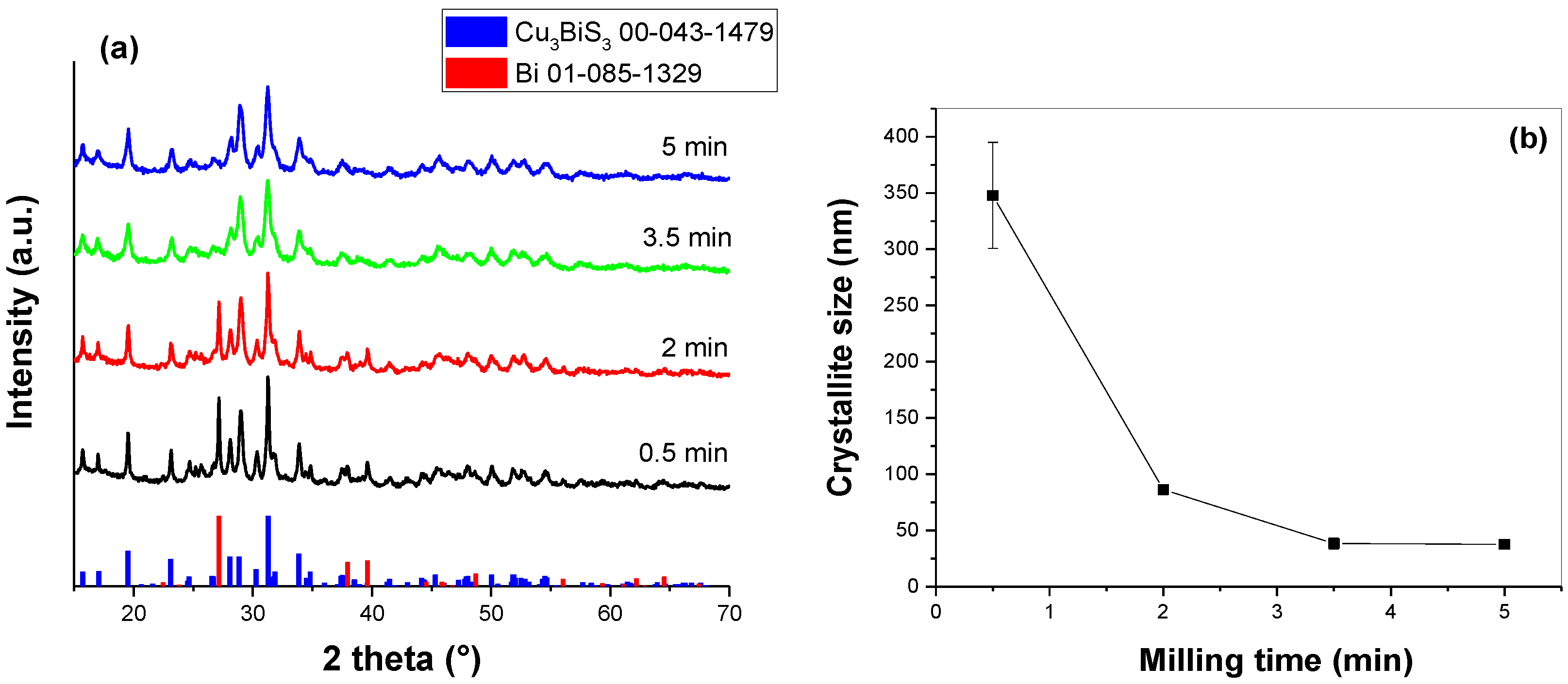
3.1.1. X-ray Diffraction

The kinetics of the mechanochemical synthesis of wittichenite Cu3BiS3 was investigated by X-ray diffraction (XRD). The XRD patterns were observed at different milling times (0.5, 2, 3.5 and 5 min), as shown in Figure 1. The desired phase for wittichenite Cu3BiS3 (PDF 00-043-1479) was identified at the shortest milling time (0.5 min) and unreacted bismuth Bi, syn (PDF 01-085-1329), is also present. After 2 min of milling, the unreacted bismuth Bi is still present. However, after 3.5 min of milling, only Cu3BiS3 as the final product is present, the unreacted Bi disappears, and the mechanochemical reaction is almost complete. A further 1.5 min of treatment did not bring about any significant changes in the XRD pattern. A substantial peak broadening reveals the obvious nanocrystalline character of the sample, and this was also established by calculations from the XRD. The estimated phase compositions obtained by Rietveld refinement match well with the analysis of the XRD patterns described above. Specifically, the content of unreacted elemental Bi for the reaction mixtures milled for 0.5 min and 2 min was 8.6 ± 0.6 and 7.3 ± 0.6%, respectively. Afterwards, a Bi0 phase was not present.
By means of Rietveld refinement, the crystallite size of the produced Cu3BiS3 was also estimated (Figure 1b). During its rapid formation after 5 min, the crystals are slightly less than 350 nm in size and the size drops well below 100 nm for all other cases. Interestingly, the crystallite size of the non-reacted bismuth is 67 ± 5 nm and 61 ± 5 nm in the mixtures after 0.5 and 3.5 min, respectively. The crystallite size for the Cu3BiS3 phase obtained after 3.5 and 5 min is practically identical (38 ± 9 nm), meaning that the supply of more energy does not lead to a larger reaction. In the case of these two samples, microstrain also comes into play, being 0.72 ± 0.22 and 0.65 ± 0.17 for the product obtained after 3.5 and 5 min, respectively. This means that the crystal lattice becomes deformed as the reaction completion approaches. Hussain et al. [22] prepared Cu3BiS3 thin films with the crystallite size from 38 to 44 nm via one-stage thermal evaporation with increasing deposition temperatures up to 400 °C. Santhanapriya et al. [38] also synthesized the pure single-phase orthorhombic structure of Cu3BiS3 with an average crystallite size of 38 nm. These reported results are in good agreement with our results.
The added value of this research strategy for preparing Cu3BiS3 nanoparticles by mechanochemical synthesis is, namely, its economic affordability: its very rapid synthesis, solvent-free character, ambient pressure and room temperature conditions. The approach is reproducible, ensuring high yield, is simple and is easy to operate. The final pure sample prepared after only 5 min of milling was selected for further characterization of the structural and microstructural properties as well being investigated from optical and optoelectrical points of view.

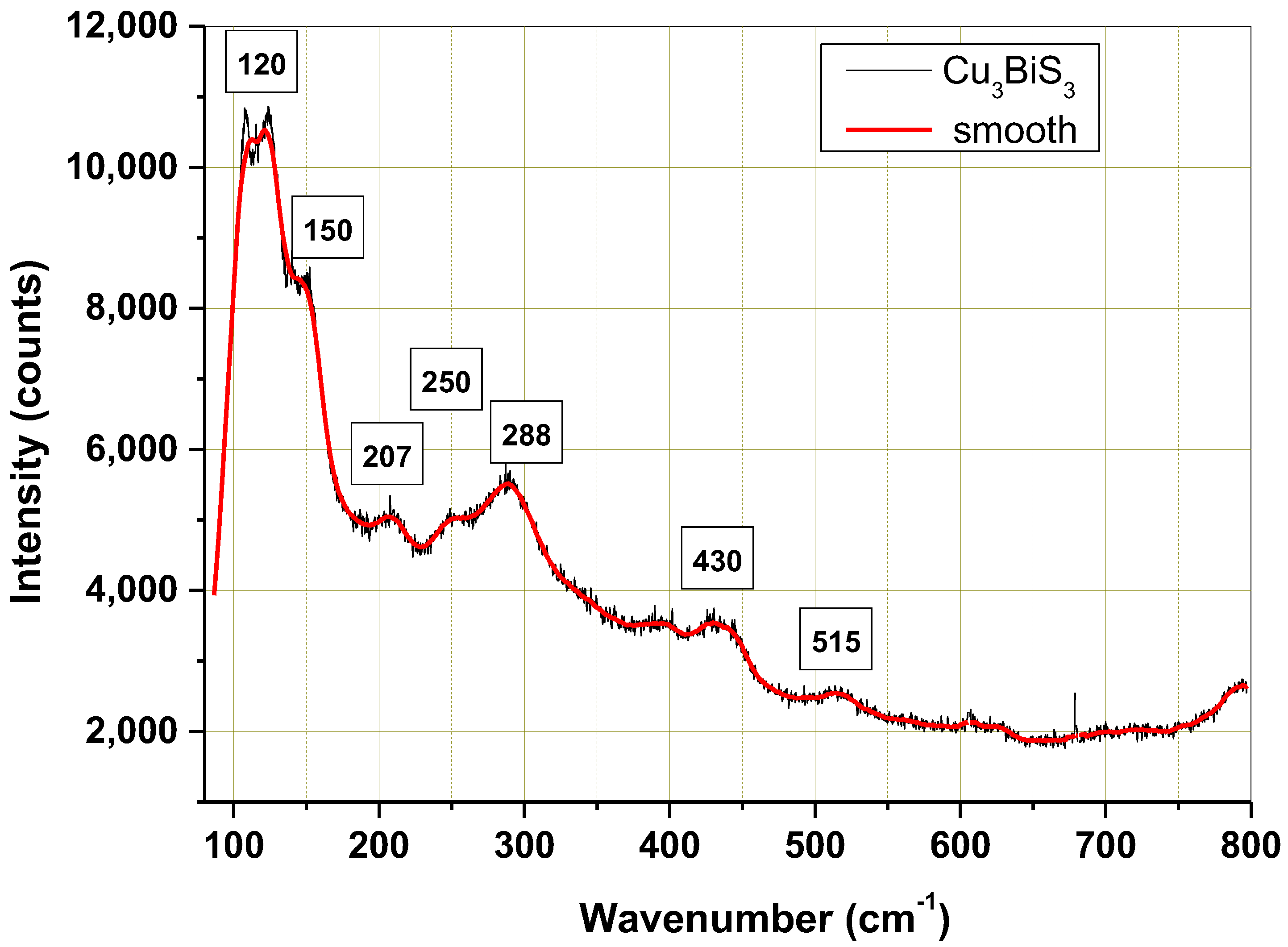
3.1.2. Raman Spectroscopy

The results of Raman spectroscopy recorded between 80 and 800 cm−1 confirming the crystallinity and structural phase analysis of the prepared Cu3BiS3 sample are shown in Figure 2. The representative micro-Raman spectrum obtained using laser excitation at 514 nm shows modes of 120, 150, 207, 250, 288, 430 and 515 cm−1. The observed modes are close to those of the Cu3BiS3 phase reported in the literature [18,22,39,40,41] and RRUFF database. The measured spectrum from the micro-Raman measurements confirmed that the synthesized Cu3BiS3 is phase pure and the results are in agreement with the measurements obtained from the XRD analysis (Figure 1).

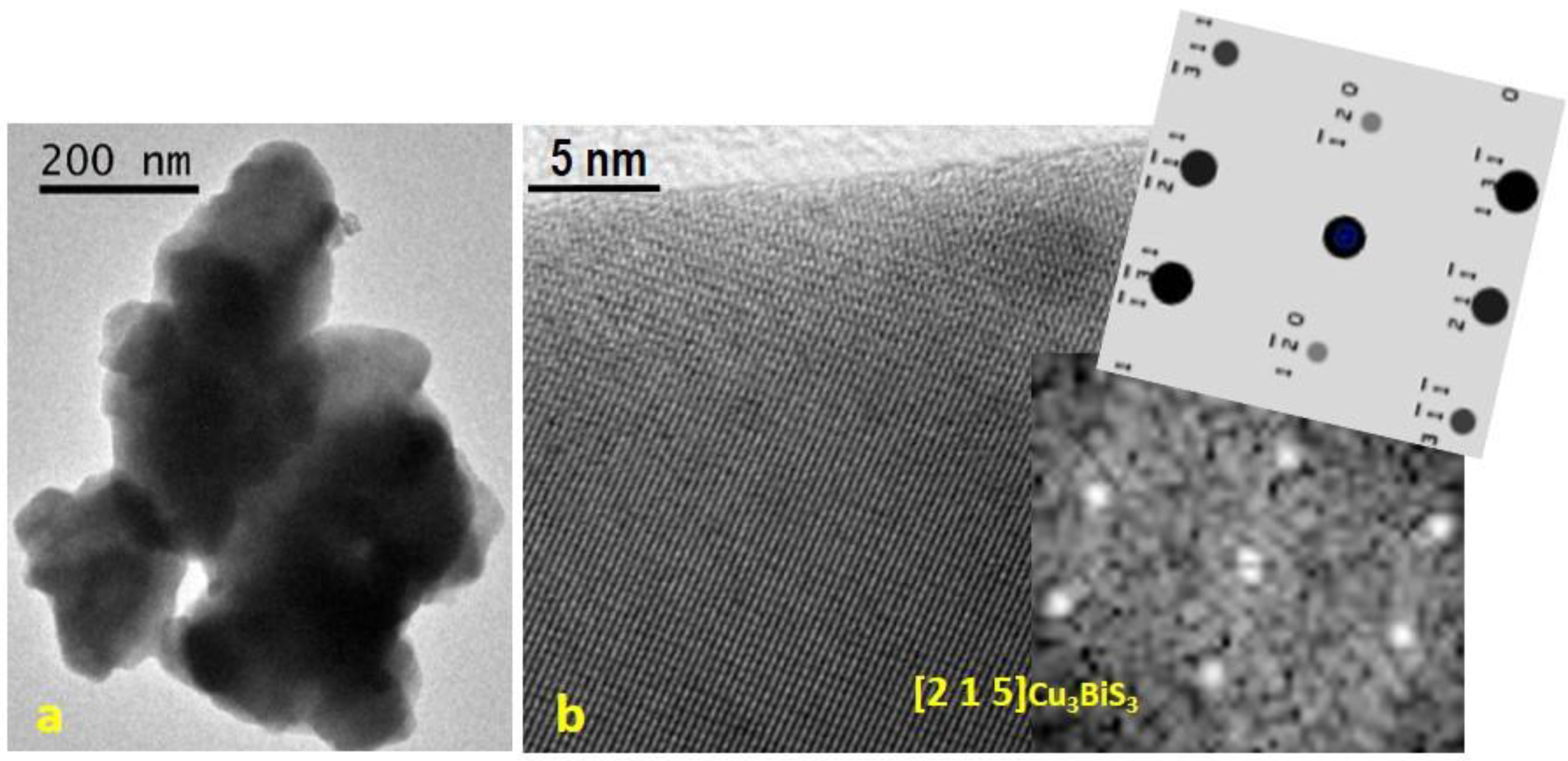
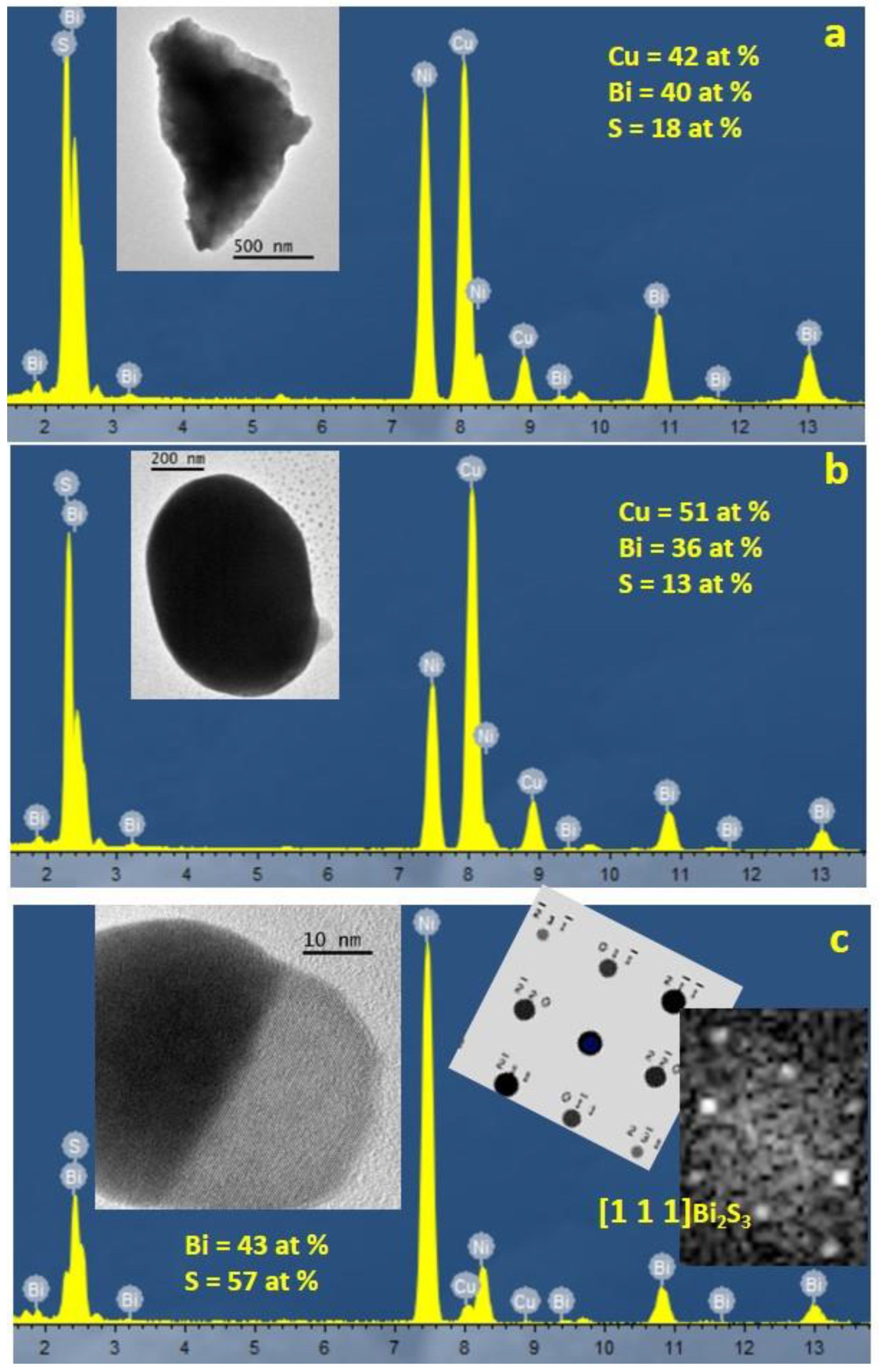
3.2. Microstructural Characterization

The wittichenite Cu3BiS3 sample was further described by TEM and related techniques. A low-magnification image of the sample is presented in Figure 3a, showing the typical appearance of mechanochemically synthesized samples, where small crystallites are agglomerated, forming large particles. The medium particle size is between 0.5 and 2 µm. A HRTEM study indicates that the nanocrystals can be indexed in an orthorhombic symmetry consistent with the Cu3BiS3 structure (space group P212121 with lattice parameters a = 7.723 Å, b = 10.395 Å and c = 6.716 Å, α = β = γ = 90°), in good agreement with the XRD results. A representative micrograph directed along the [2 1 5]Cu3BiS3 zone axis is shown in Figure 3b and the appropriate FFT and simulated EDP are inset. However, the Cu3BiS3 sample was unstable under the beam irradiation. It was found that small nanocrystallites of Bi2S3 are ejected from the as-received Cu3BiS3 during TEM analysis. This was confirmed by EDX analysis and the results are displayed and described in Figure 4.
An X-ray spectroscopy (EDX) study was performed to interpret the instability of the sample under the beam irradiation. EDX allowed us to determine the chemical composition of the particles before and after being irradiated, as well as that of the crystallites that were ejected out of the Cu3BiS3 particles. The composition before irradiation (EDX spectrum of a particle, Figure 4a) shows an atomic ratio in accordance with Cu3BiS3 stoichiometry (42 at % of Cu, 18 at % of Bi and 40 at % of S). However, after some minutes of irradiation, the composition changes to 51 at % of Cu, 13 at % of Bi and 36 at % of S (Figure 4b), meaning that the content of Bi and S has decreased, whereas that of Cu has increased. This composition change is due to the ejection of some small Bi2S3 crystallites out of the irradiated particle (see inset in Figure 4b,c). The HRTEM study shows that such crystallites have a structure according to the orthorhombic Bi2S3 (unit cell parameters, a = 11.15 Å, b = 11.30 Å and c = 3.98 Å, α = β = γ = 90° and space group Pbnm). A Bi2S3 nanocrystal oriented along [1 1 1]Bi2S3 is presented in Figure 4c and the corresponding FFT and the calculated EDP are inset.

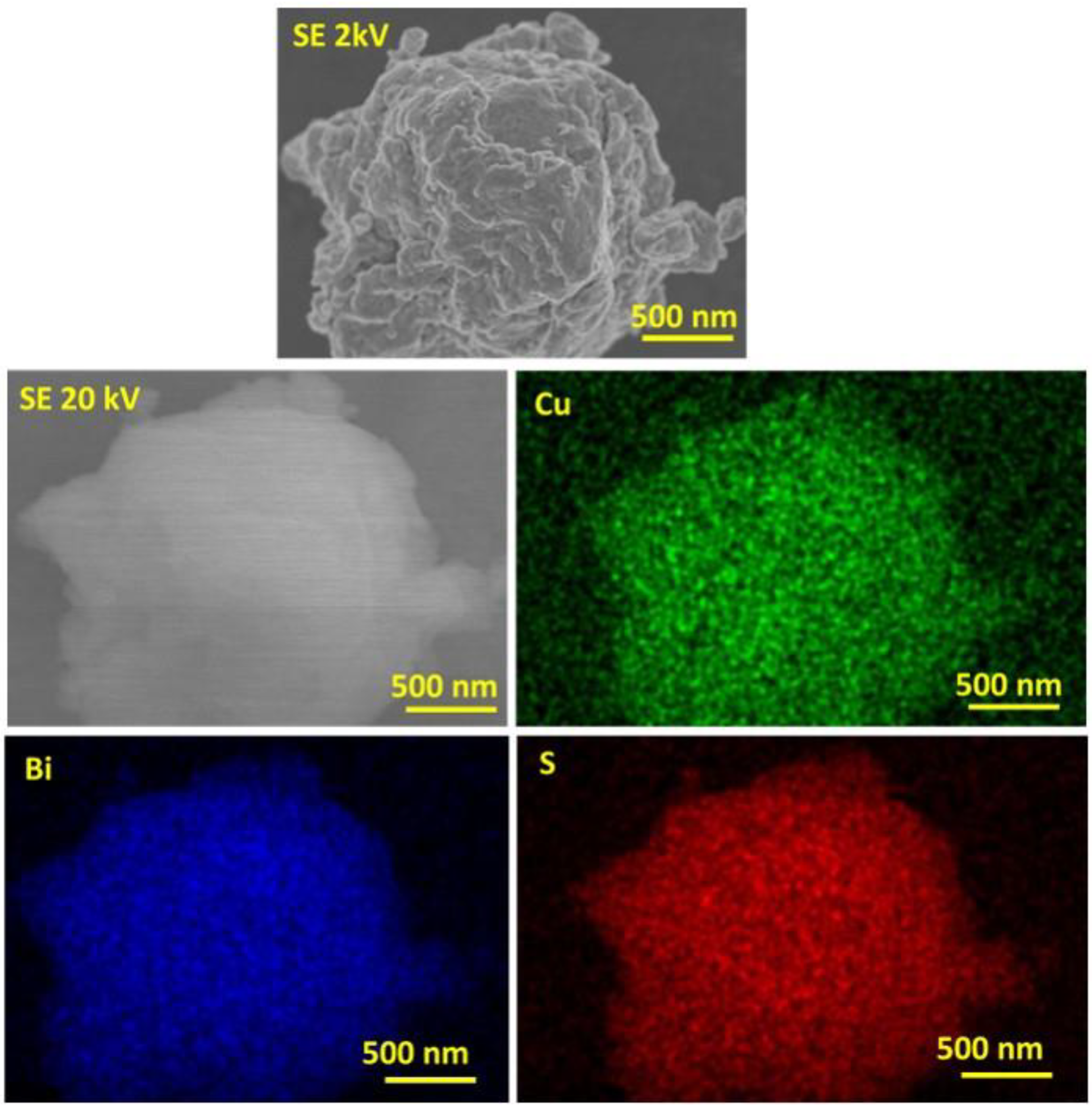
3.3. Morphological Characterization

The morphology and chemical composition of the mechanochemically synthesized Cu3BiS3 after 5 min of milling are documented by SEM study and elemental mapping analysis (Figure 5). The representative SEM image of mechanochemically synthesized Cu3BiS3 showing several grains at lower magnification is displayed in the Supplementary Materials (SM) in Figure S2. The chemical composition was also analyzed using ICP. The Cu, Bi and S elemental maps show that the three elements are homogeneously distributed thought the sample, with an elemental ratio according to a monophasic Cu3BiS3. These data are in good agreement with the ICP results, where 10 mg of Cu3BiS3 sample in 50 mL of solution gave 75.75 ppm of Cu, 85.36 ppm of Bi and 39.10 ppm of S. It must be taken into account that in the mechanosynthesis method, all of the elements that are introduced as precursors will be present in the final product of the reaction, regardless of whether or not the reaction has been completed. This was confirmed via the ICP results, which indicated the amounts of each element that were introduced into the reaction and were present in the dissolved sample.

3.4. Specific Surface Area Measurement

The nanosized crystallites usually possess a high specific surface area; however, they have a tendency to form agglomerates because of their small size. The surface properties were investigated by the low-temperature nitrogen adsorption method. The specific surface area values increased with the increase in the milling time from 0.7 m2g−1 to 2.7 m2g−1. The highest value 2.7 m2g−1 was measured for the pure Cu3BiS3 sample milled after 5 min. The measured values are in accordance with those reported for other mechanochemically prepared ternary sulfides [33,42]. Contrary to our mechanochemical synthesis, it is possible to obtain Cu3BiS3 with a higher specific surface area around 17 m2g−1 when applying the biomolecule-assisted hydrothermal and solvothermal method [19].

3.5. Optical Properties

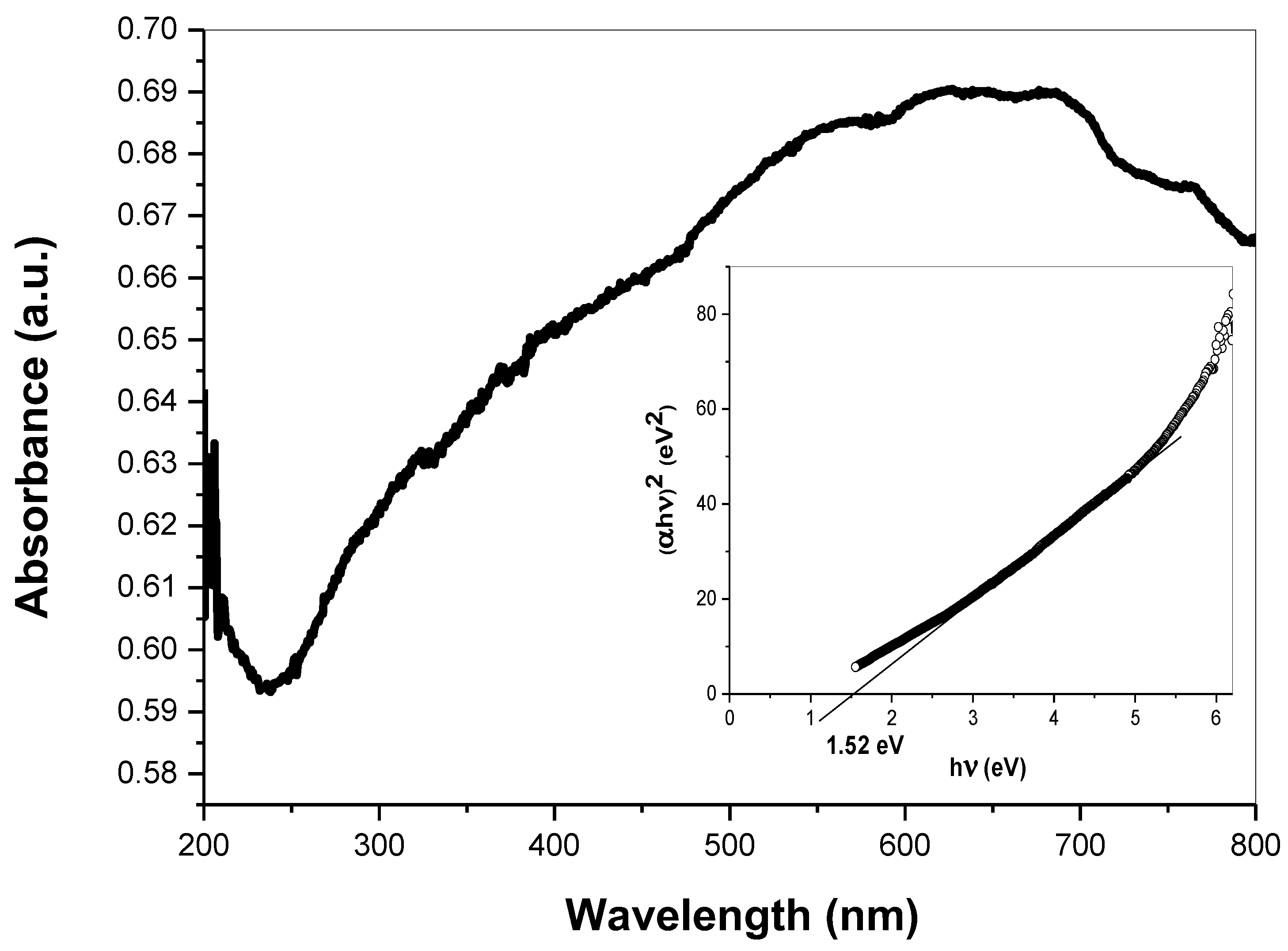
3.5.1. UV–Vis Spectroscopy

The absorption properties of mechanochemically synthesized wittichenite Cu3BiS3 prepared after 5 min of milling were investigated using UV–Vis absorption microscopy. The measured spectrum in the range from 200 nm to 800 nm, displayed in Figure 6, shows a broad absorption peak with increasing absorbance from 250 nm and a maximum at approximately 670 nm.
The determined optical bandgap, 1.52 eV, calculated by the utilization of the Tauc equation (Equation (2)) and displayed by the Tauc plot in the inset of Figure 6 is in good accordance with previous reports [4,18,19,43,44]. Yan et al. [18] and Chakraborty et al. [44] used a hot-injection method to synthesize wittichenite nanocrystals with optical bandgaps of 1.56 eV and 1.5 eV, respectively. Viezbicke et al. [4] prepared Cu3BiS3 by a solvothermal method with a direct bandgap at approximately 1.5 eV. Deshmukh et al. [43] prepared Cu3BiS3 thin films exhibiting the optical bandgap 1.56 eV using the chemical bath deposition (CBD) technique. The obtained bandgap value of Cu3BiS3 is greater than the bandgap of bulk Cu3BiS3 (1.40 eV) [3], which can be attributed to the quantum confinement effect in the nanocrystals. This bandgap value corresponds to the optimum for solar cells and confirms that wittichenite is a suitable material for use in solar cells.

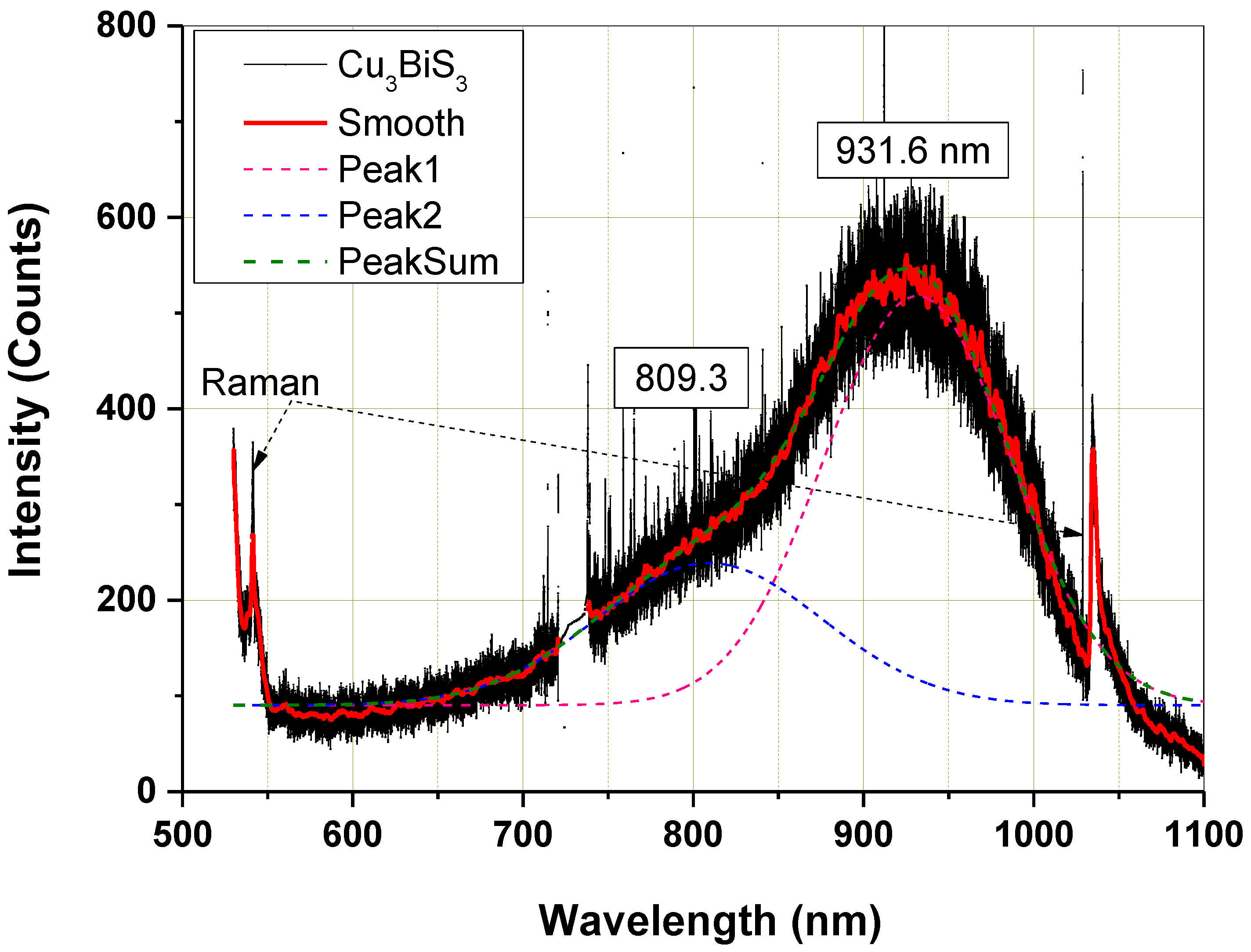
3.5.2. Micro-Photoluminescence Spectroscopy

Figure 7 shows the measured micro-PL spectrum obtained upon excitation of the sample with a wavelength of 514 nm. In the spectrum, a broad emission peak is located near 931.6 nm (1.33 eV) with an onset at 809.3 nm (1.53 eV), which agrees with the measured results obtained in a previous report [45]. The values obtained that correspond to the fitted PL Cu3BiS3 peaks are in good agreement with the published bandgap data for bulk Cu3BiS3 (around 1.40 eV) [3].

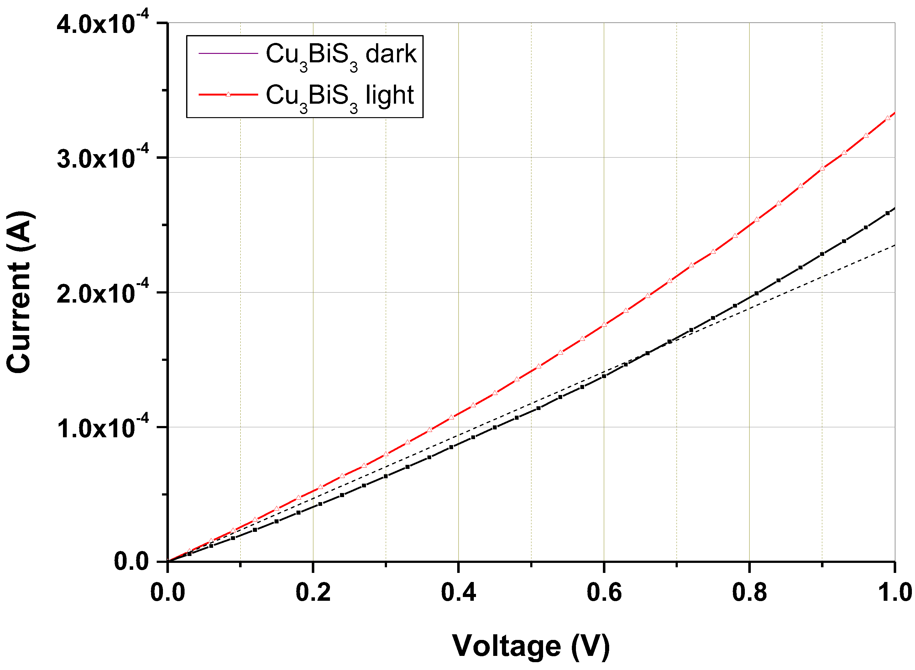
3.6. Optoelectrical Properties

The optoelectrical properties of the Cu3BiS3 powder nanocrystals dispersed on interdigital contacts from solution were verified by measuring the current–voltage (I–V) characteristics in the dark and under focused halogen light illumination. In doing so, we assumed that in the thin dispersed layer on Au fingers, active bridges from the nanopowder will be created in the gaps for the possibility of measuring electrical and optoelectrical parameters. Our measurements were carried out to confirm the fact that the prepared nanocrystalline powder exhibits suitable electrical conductivity and photosensitivity. This was confirmed by the measurement of the current–voltage characteristics, as shown in Figure 8. The I–V characteristics show only a slightly nonlinear dependence on the voltage, which indicates the formation of an acceptable ohmic contact between the Au fingers of the interdigital structure. Under intense illumination, a thin layer of dispersed Cu3BiS3 nanocrystals shows an increase in the current due to the generation of charge carriers, which causes an increase in the photo-responsive current. The generated photo-responsive current shows a 26% increase at 1V compared to the current in the dark for the measured sample.
The I–V characteristics of the synthetized Cu3BiS3 nanostructures and their photo-responsive properties have been previously studied in [11] and a similar nanocrystal film prepared by drop-casted Cu3BiS3 nano ink on glass is presented in [18], both of which show comparable optoelectrical properties.

4. Conclusions

In this research, the very rapid one-step mechanochemical synthesis of wittichenite Cu3BiS3 from copper, bismuth and sulfur precursors using high-energy milling after only 5 min in a planetary mill is reported. The crystallite size of the orthorhombic Cu3BiS3 calculated by Rietveld refinement was around 38 nm ± 9 nm. Micro-Raman spectroscopy confirmed the purity of the synthesized Cu3BiS3. The nanocrystalline character of the Cu3BiS3 was also endorsed by transmission electron microscopy. The morphology characterization demonstrated the homogeneity of the prepared sample. The morphological characterization using SEM and the surface properties investigated by the low-temperature nitrogen adsorption showed that the prepared nanocrystallites are agglomerated into micron-scale particles that exhibit specific surface areas below 3 m2g−1. The medium particle size of wittichenite Cu3BiS3 is between 0.5 and 2 µm. The optical bandgap of Cu3BiS3 was detected to be 1.52 eV. The Cu3BiS3 nanocrystals show ~26% enhancement on the photo-responsive current, which proves that wittichenite Cu3BiS3 exhibits acceptable photoelectric properties and provides a prerequisite for use in photovoltaics. The present research shows that mechanochemical synthesis is a feasible way to prepare Cu3BiS3 nanocrystals in an environmentally friendly manner that are potentially applicable in solar cells.

Supplementary Materials

The following supporting information can be downloaded at: https://www.mdpi.com/article/10.3390/cryst13030487/s1, Figure S1: Particle size analysis of the used precursors: (a) Cu, (b) Bi, (c) S; Figure S2: SEM image of mechanochemically synthesized Cu3BiS3 after 5 min of milling at lower magnification.

Author Contributions

Conceptualization, E.D.; methodology, E.D., M.B., M.J.S., J.K. and J.K.J.; validation, E.D., M.B., M.J.S., J.K. and J.K.J.; investigation, E.D., M.B., M.J.S., J.K. and J.K.J.; writing—original draft preparation, E.D.; writing—review and editing, M.B., M.J.S., J.K. and J.K.J.; visualization, E.D., M.B., M.J.S., J.K. and J.K.J. All authors have read and agreed to the published version of the manuscript.

Funding

This research was supported by the Slovak Research and Development Agency (contract No. APVV-18-0357 and APVV-20-0437) and Slovak Grant Agency VEGA (projects 2/0112/22 and 2/0084/23).

Data Availability Statement

The data presented in this study are available on request from the corresponding author.

Acknowledgments

The authors would like to thank R. Bureš for performing the PSD analyses of the used precursors.

Conflicts of Interest

The authors declare no conflict of interest. The funders had no role in the design of the study; in the collection, analyses, or interpretation of data; in the writing of the manuscript, or in the decision to publish the results.

References

  1. Kehoe, A.B.; Temple, D.J.; Watson, G.W.; Scanlon, D.O. Cu(3)MCh(3) (M = Sb, Bi; Ch = S, Se) as candidate solar cell absorbers: Insights from theory. PCCP 2013, 15, 15477–15484. [Google Scholar] [CrossRef] [PubMed]
  2. Deshmukh, S.G.; Kheraj, V. A comprehensive review on synthesis and characterizations of Cu3BiS3 thin films for solar photovoltaics. Nanotechnol. Environ. Eng. 2017, 2, 15. [Google Scholar] [CrossRef] [Green Version]
  3. Gerein, N.J.; Haber, J.A. One-step synthesis and optical and electrical properties of thin film Cu3BiS3 for use as a solar absorber in photovoltaic devices. Chem. Mater. 2006, 18, 6297–6302. [Google Scholar] [CrossRef]
  4. Viezbicke, B.D.; Birnie, D.P. Solvothermal Synthesis of Cu3BiS3 Enabled by Precursor Complexing. Acs Sustain. Chem. Eng. 2013, 1, 306–308. [Google Scholar] [CrossRef]
  5. Yang, Y.; Wu, H.X.; Shi, B.Z.; Guo, L.L.; Zhang, Y.J.; An, X.; Zhang, H.; Yang, S.P. Hydrophilic Cu3BiS3 Nanoparticles for Computed Tomography Imaging and Photothermal Therapy. Part. Part. Syst. Charact. 2015, 32, 668–679. [Google Scholar] [CrossRef]
  6. Lu, R.; Zhu, J.Y.; Yu, C.W.; Nie, Z.L.; Gao, Y. Cu(3)BiS(3)Nanocrystals as Efficient Nanoplatforms for CT Imaging Guided Photothermal Therapy of Arterial Inflammation. Front. Bioeng. Biotechnol. 2020, 8. [Google Scholar] [CrossRef]
  7. Li, A.; Li, X.; Yu, X.J.; Li, W.; Zhao, R.Y.; An, X.; Cui, D.X.; Chen, X.Y.; Li, W.W. Synergistic thermoradiotherapy based on PEGylated Cu3BiS3 ternary semiconductor nanorods with strong absorption in the second near-infrared window. Biomaterials 2017, 112, 164–175. [Google Scholar] [CrossRef]
  8. Estrella, V.; Nair, M.T.S.; Nair, P.K. Semiconducting Cu3BiS3 thin films formed by the solid-state reaction of CuS and bismuth thin films. Semicond. Sci. Technol. 2003, 18, 190–194. [Google Scholar] [CrossRef]
  9. Chen, D.; Shen, G.; Tang, K.; Liu, X.; Qian, Y.; Zhou, G. The synthesis of Cu3BiS3 nanorods via a simple ethanol-thermal route. J. Cryst. Growth 2003, 253, 512–516. [Google Scholar] [CrossRef]
  10. Li, J.J.; Han, X.X.; Zhao, Y.; Li, J.; Wang, M.; Dong, C. One-step synthesis of Cu3BiS3 thin films by a dimethyl sulfoxide (DMSO)-based solution coating process for solar cell application. Sol. Energy Mater. Sol. Cells 2018, 174, 593–598. [Google Scholar] [CrossRef]
  11. Manimozhi, T.; Archana, J.; Ramamurthi, K. Shape controlled synthesis of Cu3BiS3 nano- and microstructures by PEG assisted solvothermal method and functional properties. Ceram. Int. 2018, 44, 15385–15392. [Google Scholar] [CrossRef]
  12. Murali, B.; Krupanidhi, S.B. Tailoring the Band Gap and Transport Properties of Cu3BiS3 Nanopowders for Photodetector Applications. J. Nanosci. Nanotechnol. 2013, 13, 3901–3909. [Google Scholar] [CrossRef]
  13. Yan, J.M.; Yu, J.; Zhang, W.J.; Li, Y.N.; Yang, X.Y.; Li, A.M.; Yang, X.K.; Wang, W.; Wang, J.Q. Synthesis of Cu3BiS3 and AgBiS2 crystallites with controlled morphology using hypocrellin template and their catalytic role in the polymerization of alkylsilane. J. Mater. Sci. 2012, 47, 4159–4166. [Google Scholar] [CrossRef]
  14. Aup-Ngoen, K.; Thongtem, S.; Thongtem, T. Cyclic microwave-assisted synthesis of Cu3BiS3 dendrites using L-cysteine as a sulfur source and complexing agent. Mater. Lett. 2011, 65, 442–445. [Google Scholar] [CrossRef]
  15. Zeng, Y.P.; Li, H.X.; Qu, B.H.; Xiang, B.Y.; Wang, L.; Zhang, Q.L.; Li, Q.H.; Wang, T.H.; Wang, Y.G. Facile synthesis of flower-like Cu3BiS3 hierarchical nanostructures and their electrochemical properties for lithium-ion batteries. Crystengcomm 2012, 14, 550–554. [Google Scholar] [CrossRef]
  16. Shen, G.Z.; Chen, D.; Tang, K.B.; Qian, Y.T. Synthesis of ternary sulfides Cu(Ag)-Bi-S coral-shaped crystals from single-source precursors. J. Cryst. Growth 2003, 257, 293–296. [Google Scholar] [CrossRef]
  17. Deng, M.J.; Shen, S.L.; Zhang, Y.J.; Xu, H.R.; Wang, Q.B. A generalized strategy for controlled synthesis of ternary metal sulfide nanocrystals. New J. Chem. 2014, 38, 77–83. [Google Scholar] [CrossRef]
  18. Yan, C.; Gu, E.N.; Liu, F.Y.; Lai, Y.Q.; Li, J.; Liu, Y.X. Colloidal synthesis and characterizations of wittichenite copper bismuth sulphide nanocrystals. Nanoscale 2013, 5, 1789–1792. [Google Scholar] [CrossRef]
  19. Aup-Ngoen, K.; Dumrongrojthanath, P.; Thongtem, T.; Thongtem, S. Effect of medium solvents on crystalline degree and specific surface area of Cu3BiS3 nanoparticles synthesised by biomolecule-assisted hydrothermal and solvothermal methods. Int. J. Nanotechnol. 2017, 14, 22–30. [Google Scholar] [CrossRef]
  20. Liu, S.; Wang, X.B.; Nie, L.Y.; Chen, L.J.; Yuan, R. Spray pyrolysis deposition of Cu3BiS3 thin films. Thin Solid Film. 2015, 585, 72–75. [Google Scholar] [CrossRef]
  21. Zhong, J.S.; Xiang, W.D.; Cai, Q.; Liang, X.J. Synthesis, characterization and optical properties of flower-like Cu3BiS3 nanorods. Mater. Lett. 2012, 70, 63–66. [Google Scholar] [CrossRef]
  22. Hussain, A.; Luo, J.T.; Fan, P.; Liang, G.X.; Su, Z.H.; Ahmed, R.; Ali, N.; Wei, Q.P.; Muhammad, S.; Chaudhry, A.R.; et al. p-type Cu3BiS3 thin films for solar cell absorber layer via one stage thermal evaporation. Appl. Surf. Sci. 2020, 505, 144597. [Google Scholar] [CrossRef]
  23. Huang, D.W.; Li, L.T.; Wang, K.; Li, Y.; Feng, K.; Jiang, F. Wittichenite semiconductor of Cu3BiS3 films for efficient hydrogen evolution from solar driven photoelectrochemical water splitting. Nat. Commun. 2021, 12. [Google Scholar] [CrossRef] [PubMed]
  24. Fazal, T.; Iqbal, S.; Shah, M.Z.; Mahmood, Q.; Ismail, B.; Alsaab, H.O.; Awwad, N.S.; Ibrahium, H.A.; Elkaeed, E.B. Optoelectronic, structural and morphological analysis of Cu3BiS3 sulfosalt thin films. Results Phys. 2022, 36, 105453. [Google Scholar] [CrossRef]
  25. James, S.L.; Adams, C.J.; Bolm, C.; Braga, D.; Collier, P.; Friscic, T.; Grepioni, F.; Harris, K.D.M.; Hyett, G.; Jones, W.; et al. Mechanochemistry: Opportunities for new and cleaner synthesis. Chem. Soc. Rev. 2012, 41, 413–447. [Google Scholar] [CrossRef] [Green Version]
  26. de Oliveira, P.F.M.; Torresi, R.M.; Emmerling, F.; Camargo, P.H.C. Challenges and opportunities in the bottom-up mechanochemical synthesis of noble metal nanoparticles. J. Mater. Chem. A 2020, 8, 16114–16141. [Google Scholar] [CrossRef]
  27. Do, J.L.; Friscic, T. Mechanochemistry: A Force of Synthesis. Acs Cent. Sci. 2017, 3, 13–19. [Google Scholar] [CrossRef] [Green Version]
  28. Baláž, M.; Vella-Zarb, L.; Hernández, J.G.; Halasz, I.; Crawford, D.E.; Krupička, M.; André, V.; Niidu, A.; García, F.; Maini, L.; et al. Mechanochemistry: A disruptive innovation for the industry of the future. Chim. Oggi-Chem. Today 2019, 37. [Google Scholar]
  29. Baláž, P.; Achimovičová, M.; Baláž, M.; Billik, P.; Cherkezova-Zheleva, Z.; Criado, J.M.; Delogu, F.; Dutková, E.; Gaffet, E.; Gotor, F.J.; et al. Hallmarks of mechanochemistry: From nanoparticles to technology. Chem. Soc. Rev. 2013, 42, 7571–7637. [Google Scholar] [CrossRef] [Green Version]
  30. Dutková, E.; Sayagues, M.J.; Briančin, J.; Zorkovská, A.; Bujňáková, Z.; Kováč, J.; Kováč, J.J.; Baláž, P.; Ficeriová, J. Synthesis and characterization of CuInS2 nanocrystalline semiconductor prepared by high-energy milling. J. Mater. Sci. 2016, 51, 1978–1984. [Google Scholar] [CrossRef]
  31. Dutkova, E.; Bujnakova, Z.; Kovac, J.; Skorvanek, I.; Sayagues, M.J.; Zorkovska, A.; Kovac, J.; Balaz, P. Mechanochemical synthesis, structural, magnetic, optical and electrooptical properties of CuFeS2 nanoparticles. Adv. Powder Technol. 2018, 29, 1820–1826. [Google Scholar] [CrossRef]
  32. Dutkova, E.; Sayagues, M.J.; Fabian, M.; Kovac, J.; Kovac, J.; Balaz, M.; Stahorsky, M. Mechanochemical synthesis of ternary chalcogenide chalcostibite CuSbS2 and its characterization. J. Mater. Sci.-Mater. Electron. 2021, 32, 22898–22909. [Google Scholar] [CrossRef]
  33. Dutkova, E.; Sayagues, M.J.; Fabian, M.; Balaz, M.; Achimovicova, M. Mechanochemically synthesized ternary chalcogenide Cu3SbS4 powders in a laboratory and an industrial mill. Mater. Lett. 2021, 291, 129566. [Google Scholar] [CrossRef]
  34. Dutková, E.; Sayagués, M.J.; Fabián, M.; Baláž, M.; Kováč, J.; Kováč, J., Jr.; Stahorský, M.; Achimovičová, M.; Lukáčová Bujňáková, Z. Nanocrystalline Skinnerite (Cu3SbS3) Prepared by High-Energy Milling in a Laboratory and an Industrial Mill and Its Optical and Optoelectrical Properties. Molecules 2023, 28, 326. [Google Scholar] [CrossRef] [PubMed]
  35. Coelho, A.A. TOPAS and TOPAS-Academic: An optimization program integrating computer algebra and crystallographic objects written in C plus. J. Appl. Crystallogr. 2018, 51, 210–218. [Google Scholar] [CrossRef] [Green Version]
  36. Evans, J.S.O. Advanced Input Files & Parametric Quantitative Analysis Using Topas. Extending Reach. Powder Diffr. Model. User Defin. Macros 2010, 651, 1–9. [Google Scholar] [CrossRef]
  37. Rodriguez-Carvajal, J.; Roisnel, T. Line Broadening Analysis Using FullProf*: Determination of Microstructural Properties. In Materials Science Forum; Trans Tech Publications Ltd.: Bäch SZ, Switzerland, 2004; Volume 443, pp. 123–126. [Google Scholar]
  38. Santhanapriya, R.; Muthukannan, A.; Sivakumar, G.; Mohanraj, K. Solvothermal-Assisted Synthesis of Cu3XS3 (X = Bi and Sb) Chalcogenide Nanoparticles. Synth. React. Inorg. Met.-Org. Nano-Met. Chem. 2016, 46, 1388–1394. [Google Scholar] [CrossRef]
  39. Whittles, T.J.; Veal, T.D.; Savory, C.N.; Yates, P.J.; Murgatroyd, P.A.E.; Gibbon, J.T.; Birkett, M.; Potter, R.J.; Major, J.D.; Durose, K.; et al. Band Alignments, Band Gap, Core Levels, and Valence Band States in Cu3BiS3 for Photovoltaics. ACS Appl. Mater. Interfaces 2019, 11, 27033–27047. [Google Scholar] [CrossRef]
  40. Yakushev, M.V.; Maiello, P.; Raadik, T.; Shaw, M.J.; Edwards, P.R.; Krustok, J.; Mudryi, A.V.; Forbes, I.; Martin, R.W. Investigation of the Structural, Optical and Electrical Properties of Cu3BiS3 Semiconducting Thin Films. Adv. Mater. Charact. Tech. Sol. Cells Ii 2014, 60, 166–172. [Google Scholar] [CrossRef] [Green Version]
  41. Koskela, K.M.; Tadle, A.C.; Chen, K.Y.; Brutchey, R.L. Solution Processing Cu3BiS3 Absorber Layers with a Thiol-Amine Solvent Mixture. Acs Appl. Energy Mater. 2021, 4, 11026–11031. [Google Scholar] [CrossRef]
  42. Balaz, P.; Balaz, M.; Achimovicova, M.; Bujinakova, Z.; Dutkova, E. Chalcogenide mechanochemistry in materials science: Insight into synthesis and applications (a review). J. Mater. Sci. 2017, 52, 11851–11890. [Google Scholar] [CrossRef]
  43. Deshmukh, S.G.; Panchal, A.K.; Vipul, K. Chemical Bath Deposition of Cu3BiS3 Thin Films. In Proceedings of the International Conference on Condensed Matter and Applied Physics (ICC 2015), Bikaner, India, 30–31 October 2015; Volume 1728. [Google Scholar]
  44. Chakraborty, M.; Thangavel, R.; Komninou, P.; Zhou, Z.Y.; Gupta, A. Nanospheres and nanoflowers of copper bismuth sulphide (Cu3BiS3): Colloidal synthesis, structural, optical and electrical characterization. J. Alloy. Compd. 2019, 776, 142–148. [Google Scholar] [CrossRef]
  45. Li, B.; Ye, K.C.; Zhang, Y.X.; Qin, J.B.; Zou, R.J.; Xu, K.B.; Huang, X.J.; Xiao, Z.Y.; Zhang, W.J.; Lu, X.W.; et al. Photothermal Theragnosis Synergistic Therapy Based on Bimetal Sulphide Nanocrystals Rather Than Nanocomposites. Adv. Mater. 2015, 27, 1339–1345. [Google Scholar] [CrossRef] [PubMed]
Figure 1. XRD analysis of mechanochemically synthesized wittichenite Cu3BiS3: (a) XRD patterns (milling time and corresponding numbers of PDF cards of the identified crystallographic phases from the JCPDS PDF2 database are provided in the figure); (b) Cu3BiS3 crystallite size change with milling time estimated by the Rietveld refinement.
Crystals 13 00487 g001
Figure 2. Micro-Raman spectrum of mechanochemically synthesized Cu3BiS3 after 5 min of milling.
Crystals 13 00487 g002
Figure 3. (a) TEM and (b) HRTEM images of mechanochemically synthesized Cu3BiS3. The corresponding FFT and calculated EDP are inset.
Crystals 13 00487 g003
Figure 4. EDX spectra with inset of TEM/HRTEM images of Cu3BiS3 sample before irradiation (a) and after irradiation (b,c).
Crystals 13 00487 g004
Figure 5. SEM images (2 and 20 kV) of mechanochemically synthesized Cu3BiS3 after 5 min of milling and elemental mapping results (EDX at 20 kV) showing Cu, Bi and S distribution.
Crystals 13 00487 g005
Figure 6. Wavelength-dependent absorbance of mechanochemically synthesized Cu3BiS3 after 5 min of milling. The inset shows a Tauc plot for determining the optical bandgap.
Crystals 13 00487 g006
Figure 7. Wavelength-dependent micro-PL spectrum of mechanochemically synthesized Cu3BiS3 after 5 min of milling measured upon excitation of the sample with a wavelength of 514 nm.
Crystals 13 00487 g007
Figure 8. Measured current–voltage characteristics in the dark and under illumination.
Crystals 13 00487 g008
Disclaimer/Publisher’s Note: The statements, opinions and data contained in all publications are solely those of the individual author(s) and contributor(s) and not of MDPI and/or the editor(s). MDPI and/or the editor(s) disclaim responsibility for any injury to people or property resulting from any ideas, methods, instructions or products referred to in the content.

