Article

Ga2O3/Ag/Ga2O3-Laminated Film Fabricated at Room Temperature: Toward Applications in Ultraviolet Transparent Highly Conductive Electrodes

1
School of Microelectronics, Dalian University of Technology, Dalian 116602, China
2
EpiTop Optoelectronic Co., Ltd., Maanshan 243071, China
3
School of Physical Science and Technology, Inner Mongolia University, Hohhot 010021, China
4
College of Sciences, Inner Mongolia University of Technology, Hohhot 010051, China
*
Author to whom correspondence should be addressed.
These authors contributed equally to this work.
Crystals 2023, 13(7), 1018; https://doi.org/10.3390/cryst13071018
Submission received: 20 May 2023 / Revised: 18 June 2023 / Accepted: 19 June 2023 / Published: 27 June 2023
(This article belongs to the Special Issue Optoelectronics of Thin Films and Nanoparticles)

Abstract

:
Ga2O3/Ag/Ga2O3-laminated films with high electrical conductivity and ultraviolet (UV) transparency were achieved by radio frequency magnetron sputtering at room temperature (RT) on quartz glass. The influence of annealing temperature and ambient on the structural, electrical and optical properties of Ga2O3/Ag/Ga2O3-laminated films were investigated in detail. As the annealing temperature increases, the optical bandgap of the Ga2O3-laminated films widens. The Ga2O3/Ag/Ga2O3-laminated films exhibited good photoelectric performance with a figure-of-merit (FOM) value of 5.83 × 10⁻³ Ω−1, a sheet resistance of 12.55 Ω/sq, a transmittance of 95.15% at 325 nm, and an average transmittance of 77.56% (250~300 nm). All these results suggest that RT-fabricated Ga2O3/Ag/Ga2O3-laminated films show great potential in UV transparent conductive electrodes for UV optoelectronic devices and in flexible electronics.

1. Introduction

Ultraviolet (UV, λ < 400 nm) transparent and conductive metallic oxides (TCOs) are essential as electrodes in flexible electronics and UV optoelectronic devices, such as light emitting diodes (LEDs), solar-blind photodetectors, solar cells, etc. [1,2,3]. Usually, low electric resistance and high optical transmittance are the two typical figure-of-merit (FOM) parameters by which to evaluate the performance of TCOs. However, conventional TCOs, such as Sn-doped In2O3 (ITO) and Al-doped ZnO (AZO), present low transmittance in the UV region due to their small bandgaps [4,5]. As one of the ultra-wide bandgap semiconductors, Ga2O3 has emerged as an interesting alternative because of its wide bandgap (~4.9 eV) and adjustable electrical resistivity [6,7]. Orita et al. prepared Sn-doped Ga2O3 single-layer UV TCO films with the n-type conductivity of ~1 Scm−1 and optical transmittance beyond 50% at the wavelength of ~248 nm [8]. Zhu et al. prepared Si-doped Ga2O3 single-layer UV TCO films with optical transmittance up to 50% at 280 nm, electron mobility of 11.8 cm2 V−1 s−1 and carrier concentration of 2.59 × 1017 cm−3, respectively [9]. Jeon et al. obtained homoepitaxial Si-doped β-Ga2O3 single-layer UV TCO films with a conductivity of 2323 Scm−1 [10]. Despite these inspiring results, the high-cost and high-temperature fabrication, relatively low electrical properties, small wafer size and low thermal conductivity of Ga2O3 still limit it as TCO electrodes in applications for UV devices and flexible electronics.
To overcome these limitations, metal/Ga2O3-stacked or laminated structures, allowing simple, low cost and mass production at room temperature (RT), have recently been proposed due to the low resistivity, low absorption and high thermal conduction of metal materials including Ag, Au, Cu, Al, etc. Woo et al. [11] and Kim et al. [12] reported Ag/Ga2O3- and ITO/Ga2O3-bilayer UV TCO films using magnetron sputtering, where the optical transmittance and sheet resistance of the Ag/Ga2O3- and ITO/Ga2O3-bilayer UV TCO films were about 91% (380 nm), 80.94% (380 nm) and <42 Ω/sq, 58.6 Ω/sq, respectively. Zhuang et al. [13], Kim et al. [14] and Liang et al. [15] studied the properties of Ga2O3/Cu/ITO-, Ga2O3/Ag/Ga2O3- and ITO/Ga2O3/Ag/Ga2O3 -multilayer TCO films, respectively. The optical transmittance and sheet resistance of these UV TCO films are 86% (300~850 nm), 87.16% (300~350 nm), 86.4% (335 nm) and 45 Ω/sq, 8.48 Ω/sq and 3.43 Ω/sq, respectively. Furthermore, the FOM was calculated as 8.89 × 10⁻² Ω−1 and 2.98 × 10⁻² Ω−1 for Ga2O3/Cu/ITO- and Ga2O3/Ag/Ga2O3-multilayer TCO films, respectively. As for laminated Ga2O3 TCOs, magnetron sputtering was generally used to deposit Ga2O3 layers, and they were annealed in N2, air or a N2/O2 mixture ambient for further device fabrication [16]. A recent report demonstrated that high-temperature N2 annealing may cause α-Ga2O3 formation and much higher resistance states due to compensation doping [17]. The nanopores were also possibly formed which leads to poor optical transmittance. Therefore, the fabrication and thermal annealing process of Ga2O3/metal-laminated film still needs to be optimized for further applications in UV devices and flexible electronics.
In this work, the Ga2O3/Ag/Ga2O3-laminated films were fabricated by magnetron sputtering at RT. The influences of the thickness of Ag interlayer and thermal annealing temperature and ambient (i.e., Ar, O2 and vacuum) were studied systematically to facilitate the optimization of the optical and electric performance of Ga2O3/Ag/Ga2O3 TCO films. The introduction of an Ag interlayer into a Ga2O3 UV transparent electrode sharply decreased the sheet resistance of the laminated structure but with little loss of the total transmittance. Post-deposition thermal treatments under different conditions have shown an improvement in their performance and thermal stability on glass substrates for potential applications that require higher temperatures.

2. Experimental Details

The Ag and Ga2O3 targets with a purity of 99.99% were used for the sputtering of Ag and Ga2O3 films, respectively. The Ga2O3/metal/Ga2O3-laminated thin films were successively deposited on quartz glass substrates while the substrate temperature of all the samples was kept at RT. Prior to deposition, both of the two targets were pre-sputtered for 10 min to remove any surface contaminants. The quartz glass substrates were ultrasonically cleaned in acetone, isopropyl alcohol, and deionized water and then subsequently dried by N2 blowing. The bottom and top Ga2O3 layers were deposited with a radio frequency (RF) power of 50 W at a working pressure of 0.2 Pa in a pure Ar atmosphere at a flow rate of 30 sccm. The Ag interlayer was deposited under the same conditions but with a different RF power of 30 W. To study the annealing effect, post-annealing was performed in a tubular furnace equipped with a turbo pump.
The thickness of each layer was calibrated by a profilometer (ET-3000I, Kosaka, Japan) and estimated by an average deposition rate. The surface morphology of films was observed by a field emission scanning electron microscope (SEM, SU8220, Hitachi, Japan). The crystalline properties were characterized via X-ray diffractometry (XRD) (Empyrean, Malvern Panalytical, Almelo, The Netherlands) with Cu-kα (λ = 0.154056 nm) radiation. The optical properties were studied by a UV-Vis spectrophotometer (Lambda 650, PerkinElmer, Waltham, MA, USA). The electrical properties of the films were measured using the standard four-probe technique at RT.

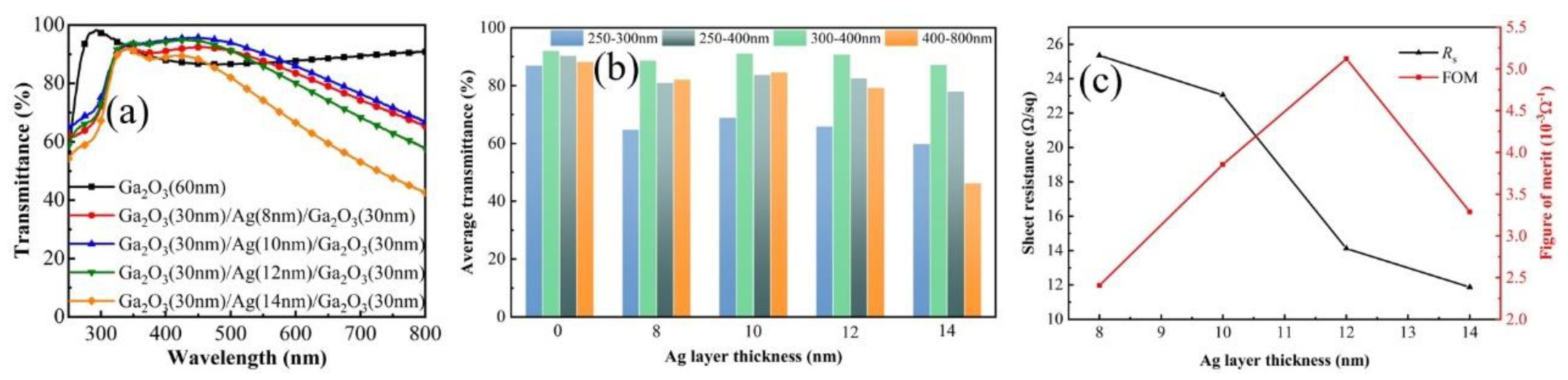
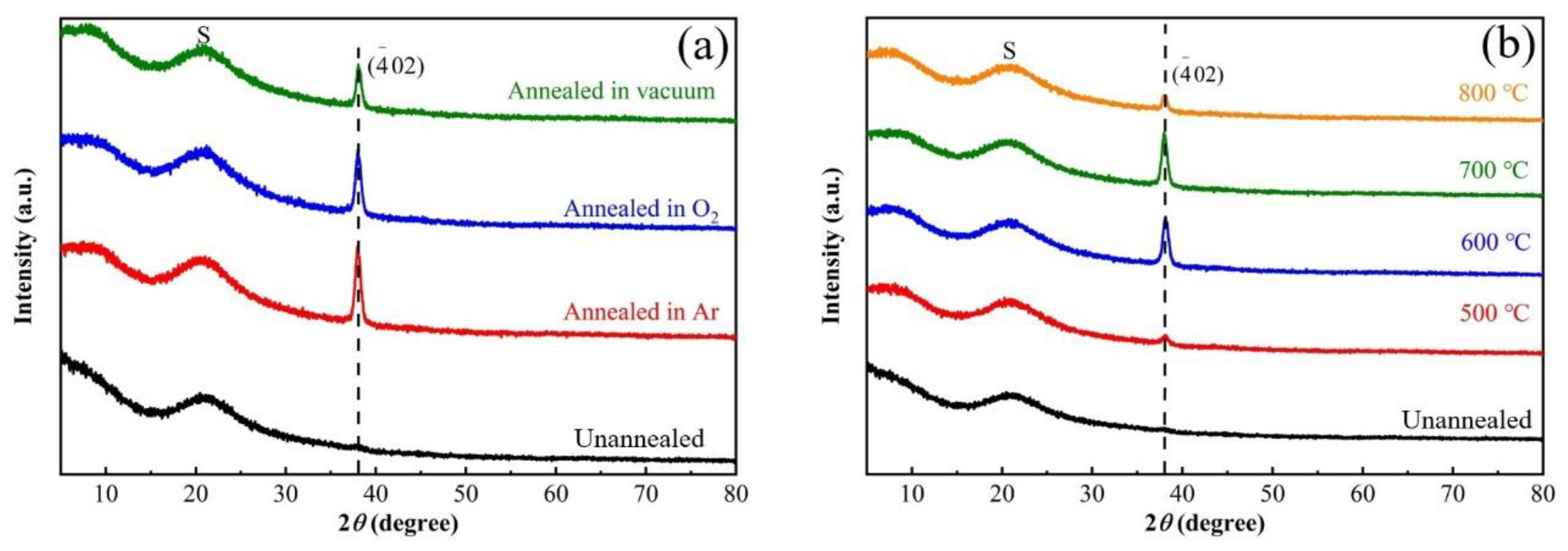
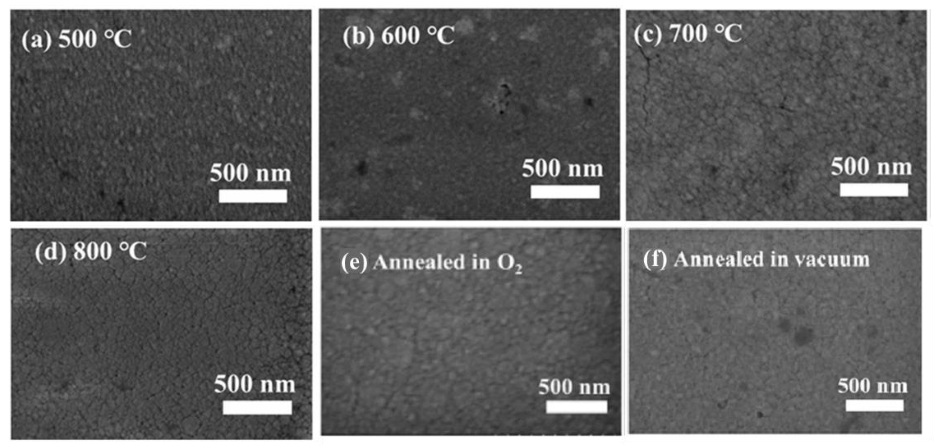
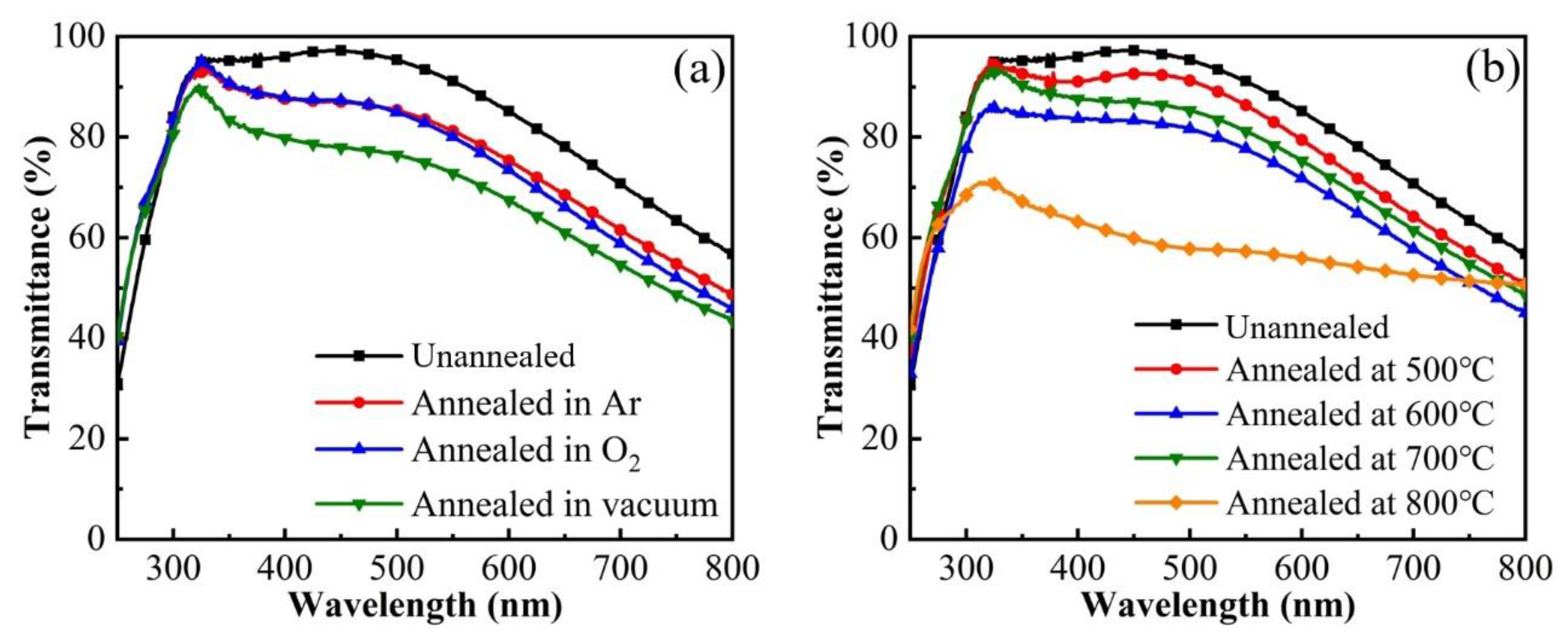
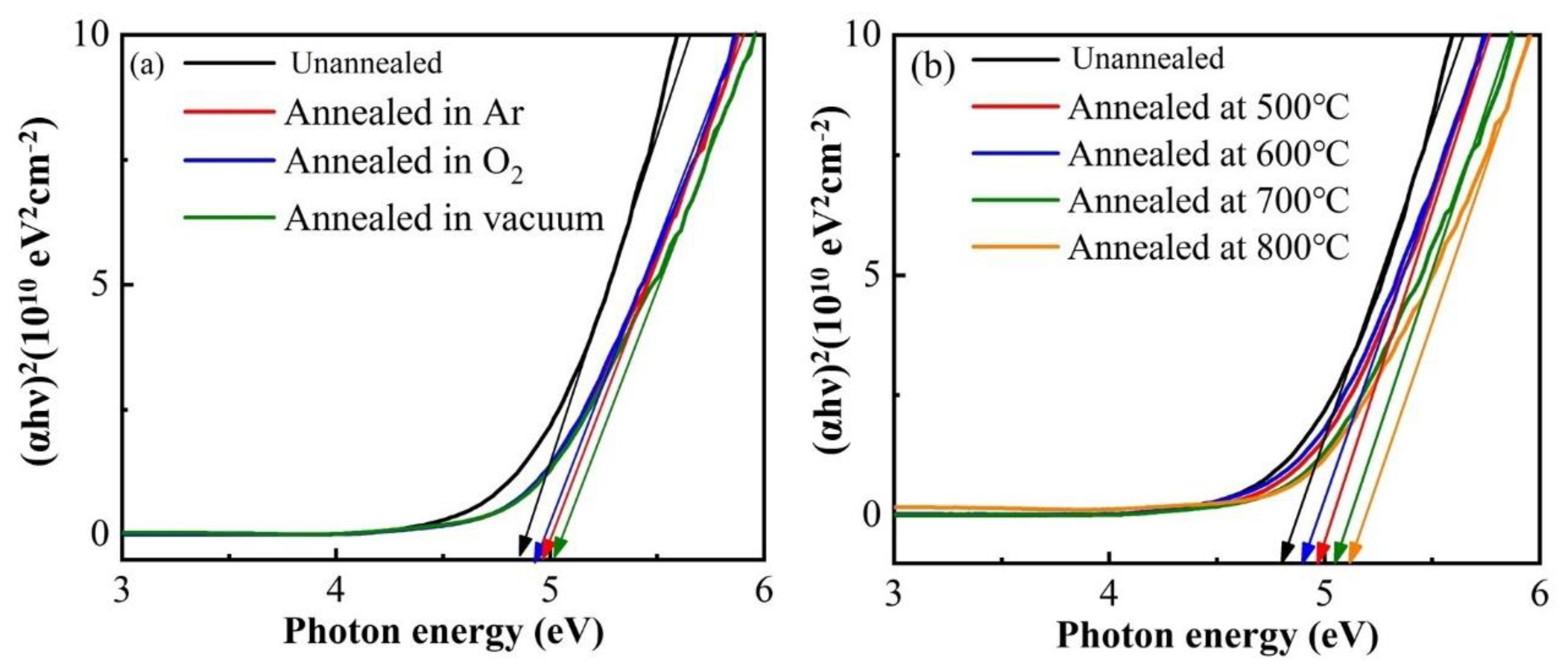
3. Results and Discussion

To study the effect of the Ag interlayer on the optical and electric properties of Ga2O3/metal/Ga2O3-laminated films, the thicknesses of both the top and bottom Ga2O3 layers were fixed at 30 nm. Figure 1 shows the optical transmittance spectra, the average transmittance and the sheet resistance of unannealed Ga2O3/Ag/Ga2O3-laminated films as functions of the thickness of the Ag interlayer. Compared with the Ga2O3 single-layer film, the Ag interlayer causes the degradation of optical transmittance, especially below 350 nm. The peak transmittance of ~95% appears at ~440 nm and shifts towards a long wavelength region. Based on the formula T = 1−RA in which T is transmittance, R is reflectance and A is absorbance, the reduction in transmittance is mainly due to the reflectance loss of the Ag interlayer as a mirror coating. The absorption loss should be considered due to the plasmon resonant absorption and free carrier absorption in some cases. While in the range of 350 to 550 nm, the transmittance of laminated films enhances a little due to the percolation effect from the imperfectly covered Ag film [18,19]. The observed low transmittance of light in the wavelength range of 700~800 nm is caused by the free carrier absorption by the additional free electrons available in the thicker Ag layer. As the thickness of Ag increases, the average transmittance in the UV band and the visible region first increases and then decreases. This phenomenon can be explained according to the surface morphology evolution of the Ag interlayer from isolated island-shaped particles to a continuous nested film and then finally to a compact homogeneous film as the Ag sputtering time increases. As light propagates into the laminated films, Rayleigh scattering and plasmon resonant absorption may occur due to the Ag island-shaped particles, leading to a reduction in transmittance even at short wavelengths. If the compact homogeneous Ag film forms, light reflection and free carrier absorption will also degrade the transmittance, especially at long wavelengths. The connected nested structure enhances the optical transmittance through macropores or micropores. It is noted that the antireflection effect of Ag mirror films will occur to enhance optical transmittance if the Ag thickness increases to a particular value. Our result is somewhat different from that obtained by Kim et al. [14], possibly because of the UV–ozone wet pretreatment which made the Ag interlayer not a compact film even at 14 nm. As mentioned in our previous work [20], the change of sheet resistance of the laminated film is mainly determined by the Ag interlayer. It is observed in Figure 1c that the black line shows the variation in the square resistance of the Ga2O3-stacked film with the thickness of the Ag layer, and the square resistance of the Ga2O3-stacked film decreases with the increase in the thickness of the Ag layer, and the resistance of these samples decreases from 25.6 Ω/sq to 11.89 Ω/sq. The reason for this is that the thickness of the Ag film gradually increases to form a continuous film, resulting in a gradual decrease in the square resistance of the Ga2O3-stacked film. The calculated FOM value reaches a maximum of 5.12 × 10⁻³ Ω−1 when the Ag film becomes continuous at a thickness of 12 nm. Table 1 gives the average transmittance, sheet resistance and FOM values of our Ga2O3-(30 nm)/Ag-(12 nm)/Ga2O3(30 nm)-laminated films compared to similar films reported in the literature at wavelengths of 300~400 nm, where the FOM is defined by the Haacke [21]:
φ = T a v 10 R s
where Tav10 is the average optical transmittance and Rs is the sheet resistance. The transmittance obtained in this work is slightly higher than the previously reported values, and the FOM values are close to those of Ref. [14].
Then, the effect of different annealing temperatures (500 °C, 600 °C, 700 °C, 800 °C) under an Ar atmosphere on the crystallinity of Ga2O3/Ag/Ga2O3-laminated films with an Ag interlayer with a thickness of 12 nm was analyzed. Figure 2a shows the X-ray diffraction pattern of unannealed and annealed Ga2O3/Ag/Ga2O3-laminated films at different temperatures, where the S part represents the quartz substrate. As can be seen from Figure 2a, the unannealed laminated film is amorphous since no obvious diffraction peak appears. The annealed laminated film has a diffraction peak corresponding to the 4 ¯ 02   orientation of β-Ga2O3 at 2θ = 38.5°. The grain size D can be calculated according to the Scherrer formula:
D = k λ β c o s θ
where β represents the XRD half-maximum width (FWHM) at   4 ¯ 02 , θ represents the Bragg diffraction angle, and λ is the X-ray wavelength. The grain sizes of samples annealed at 500~800 °C were calculated to be 10.61 nm, 12.55 nm, 12.44 nm and 11.68 nm, respectively. The average grain size increases at first and then decreases, which shows that high-temperature annealing has a significant effect on the grain size of the films. At 500 °C, a weaker diffraction peak appeared, indicating that the β-phase Ga2O3 was formed at this temperature, and the intensity of the diffraction peak gradually increased with the increase in the annealing temperature, indicating that the crystallinity of the film increased with the increase in temperature. However, the strength decreased at 800 °C since the excessively high temperature results in poor crystallization quality due to the damage of the Ag film, e.g., the oxidation of the Ag interlayer or the occurrence of Ag agglomeration [22]. This needs further investigation in another work. The increase in crystallinity can be attributed to the provision of thermal energy to the atoms during the annealing process, which helps the recovery of the crystal and reduces the defects inside the film.
The above results show that the crystallinity of Ga2O3-laminated films is the best when annealed at 700 °C. The next step is to analyze the effect of the annealing atmosphere on the crystallinity of Ga2O3-laminated films. The X-ray diffraction patterns of Ga2O3/Ag/Ga2O3-laminated films treated in different annealing atmospheres (Ar, O2, vacuum) at 700 °C are shown in Figure 2b. As can be seen from the diagram, the unannealed laminated films have no obvious diffraction peak, indicating that the laminated films are in an amorphous state. The diffraction peak of 4 ¯ 02 orientation of β-Ga2O3 appears at 2θ = 38.5°, which indicates that the annealing atmosphere did not affect the formation of crystal orientation during annealing. After annealing, the crystallinity of the β-Ga2O3 films was greatly improved, especially in Ar. The high temperature promotes the migration of surface atoms, which helps to bind Ga and O atoms into the lattice sites. On the other hand, there are many Ga dangling bonds associated with O defects at the grain boundaries. When the annealing temperature is raised, these defects are beneficial to the consolidation process to form larger grains, thus improving the crystallinity.
Figure 3 is the SEM image of the β-Ga2O3/Ag/β-Ga2O3-laminated film after annealing. Figure 3a–d are the SEM images of the surface of the β-Ga2O3/Ag/β-Ga2O3-laminated film at different annealing temperatures in an Ar atmosphere. When the annealing temperature increases from 500 °C to 800 °C, the surfaces of the films gradually become flatter and the average particle size increases, indicating an improvement in crystal quality. The surface morphology of the sample annealed in the Ar atmosphere is composed of small particles, which are closely connected with obvious boundaries between the particles. As shown in Figure 3e, the particles shrink after annealing in O2, causing the space among the particles to become wider. Figure 3f shows that the sample was annealed in a vacuum, and it can be observed that the particles are closely connected, and these results are also consistent with the above XRD results. The annealing treatment has a significant effect on the surface of the laminated film. After annealing, the atoms gain higher energy, and the crystal defect density decreases, resulting in a more uniform crystal growth and a smoother film surface. However, due to the addition of the metal interlayer, there may be a certain degree of mutual diffusion and accumulation at the interface of the interlayer during the annealing process [23].
Figure 4a shows the transmittance of a β-Ga2O3/Ag/β-Ga2O3-laminated film annealed in Ar, O2 and a vacuum. In the UV region, the transmittance of the annealed laminated film is higher than the unannealed laminated film, with the highest transmittance annealing in an Ar atmosphere. It can be seen from the SEM image that the samples annealed in O2 have larger surface voids, which increases the transmittance of the sample. For samples annealed in an Ar atmosphere, the particles are closely connected with obvious boundaries. Figure 4b shows the transmittance of a β-Ga2O3/Ag/β-Ga2O3-laminated film with different annealing temperatures in an Ar atmosphere. Compared with the unannealed Ga2O3-laminated film, the optical transmittance of the annealed Ga2O3-laminated film is improved in the UV wavelength range of 250~320 nm. This enhanced optical property by annealing is related to the increase in the refractive index [24] since a higher refractive index has a better anti-reflection effect on the Ag interlayer [25]. In addition, the Ga2O3 is transformed from amorphous to crystalline during the annealing process, which increases the optical bandgap. Therefore, the transmittance of the β-Ga2O3-laminated film after annealing is improved by the anti-reflection effect and the increase in the optical bandgap below 300 nm, and the crystallinity of the β-Ga2O3 laminated film increases with the increase in the annealing temperature, reducing the thickness of the film. The lattice defects, weakening the scattering and absorption of light, enhance the optical transmittance in the UV region [26]. In the wavelength range above 320 nm, due to the aggregation and scattering of the Ag layer, and with the further increase in the annealing temperature, the formation of Ag islands increases the scattering of light [1], resulting in a decrease in the transmittance of the Ga2O3-laminated film.
By analyzing the absorption coefficient as a function of photon energy near the fundamental absorption edge, the optical bandgap energy Eg of the β-Ga2O3/Ag/β-Ga2O3-laminated transparent conductive film is estimated using the following Tauc expression [27]:
α h ν n = A h ν E g
where α is the absorption coefficient, h is Planck’s constant, υ is the frequency of the incident light, A is the constant, and hv is the energy of the incident photon. The value of the exponent n is determined by the transition type with n = 2 (1/2) for direct (indirect) transitions. While Ga2O3 is a direct transition semiconductor, n = 2 was used in the formula. Using the interpolation of the linear fit of the plot in Figure 5a, the optical bandgaps of the stacked films annealed in O2, Ar, and a vacuum were about 4.93 eV, 4.96 eV and 5.02 eV, respectively, which are larger than that of the bulk β-Ga2O3 crystal (4.9 eV).
Figure 5b shows the optical bandgap Eg of the Ga2O3/Ag/Ga2O3-laminated films at different annealing temperatures in an Ar ambient. The Eg of the Ga2O3/Ag/Ga2O3-laminated films annealed at 500 °C, 600 °C, 700 °C and 800 °C was 4.97 eV, 4.90 eV, 5.06 eV and 5.12 eV, respectively. As the annealed temperature increased from 500 °C to 800 °C, the absorption edge shifted to a shorter wavelength, indicating an increase in Eg. When the annealing temperature increased, the crystallinity of the film improved with a gradual decrease in the number of defects, thus widening the optical bandgap.

4. Conclusions

The Ga2O3/Ag/Ga2O3-laminated films with high conductivity and UV transparency were deposited on quartz substrates via RF magnetron sputtering. As the thickness of the Ag interlayer increases, the square resistance of the laminated films gradually decreased to 11.89 Ω/sq, and the transmittance showed a trend of increasing and then decreasing. The treatment by thermal annealing was an effective way to improve the structural and optical properties of the film. The Ga2O3-laminated films were post-annealed in O2, Ar, and a vacuum to investigate the effect of different annealing conditions on the optoelectronic properties of the Ga2O3-laminated films. Through analysis and comparison, the annealed Ga2O3-stacked films all formed β-phase Ga2O3 films. Compared with the unannealed Ga2O3-stacked films, the annealed samples showed an improved transmittance in the UV wavelength range of 250~320 nm but a slight decrease in the visible wavelength range. As the annealing temperature increased, the optical band gap of the Ga2O3-stacked films increased to as high as 5.12 eV. We believe that the optical and electric performance of the presented laminated films can be further improved to serve as a UV-transparent conductive electrode if combined with several methods such as doping and defect engineering and using nonstoichiometric targets, etc.

Author Contributions

Conceptualization, K.Z. and J.Z.; methodology, K.Z. and J.Z.; validation, L.F. and L.W.; formal analysis, L.F., L.W., S.H. and J.S.; investigation, L.F. and L.W.; resources, K.Z., J.Z. and H.Z.; data curation, J.Z. and H.Z.; writing—original draft preparation, L.F. and L.W.; writing—review and editing, K.Z. and J.Z.; supervision, J.Z., H.L. and T.Y.; project administration, J.Z., H.L. and T.Y.; funding acquisition, K.Z. and J.Z. All authors have read and agreed to the published version of the manuscript.

Funding

This work was supported by the National Natural Science Foundation of China (Grant Nos. 12105033, 12164031, 61464009 and 11864029), the Fundamental Research Fund for the Central Universities (Grant No. DUT20RC(3)042), and the Science Foundation of Inner Mongolia Autonomous Region (Grant No. 2020MS06007).

Data Availability Statement

Data available on request from the corresponding author.

Conflicts of Interest

The authors declare no conflict of interest.

References

  1. Guillén, C.; Herrero, J. TCO/metal/TCO structures for energy and flexible electronics. Thin Solid Film. 2011, 520, 1–17. [Google Scholar] [CrossRef]
  2. Yu, X.; Marks, T.J.; Facchetti, A. Metal oxides for optoelectronic applications. Nat. Mater. 2016, 15, 383–396. [Google Scholar] [CrossRef] [PubMed]
  3. Spencer, J.A.; Mock, A.L.; Jacobs, A.G.; Schubert, M.; Zhang, Y.; Tadjer, M.J. A review of band structure and material properties of transparent conducting and semiconducting oxides: Ga2O3, Al2O3, In2O3, ZnO, SnO2, CdO, NiO, CuO, and Sc2O3. Appl. Phys. Rev. 2022, 9, 011315. [Google Scholar] [CrossRef]
  4. Kneissl, M.; Seong, T.Y.; Han, J.; Amano, H. The emergence and prospects of deep-ultraviolet light-emitting diode technologies. Nat. Photonics 2019, 13, 233–244. [Google Scholar] [CrossRef]
  5. Xie, C.; Lu, X.T.; Tong, X.W.; Zhang, Z.X.; Liang, F.X.; Liang, L.; Luo, L.B.; Wu, Y.C. Recent Progress in Solar-Blind Deep-Ultraviolet Photodetectors Based on Inorganic Ultrawide Bandgap Semiconductors. Adv. Funct. Mater. 2019, 29, 1806006. [Google Scholar] [CrossRef]
  6. Zhu, J.; Xu, Z.; Ha, S.; Li, D.; Zhang, K.; Zhang, H.; Feng, J. Gallium Oxide for Gas Sensor Applications: A Comprehensive Review. Materials 2022, 15, 7339. [Google Scholar] [CrossRef]
  7. Ramana, C.V.; Rubio, E.J.; Barraza, C.D.; Miranda Gallardo, A.; McPeak, S.; Kotru, S.; Grant, J.T. Chemical bonding, optical constants, and electrical resistivity of sputter-deposited gallium oxide thin films. J. Appl. Phys. 2014, 115, 043508. [Google Scholar] [CrossRef] [Green Version]
  8. Orita, M.; Ohta, H.; Hirano, M.; Hosono, H. Deep-ultraviolet transparent conductive ß-Ga2O3 thin films. Appl. Phys. Lett. 2000, 77, 4166–4168. [Google Scholar] [CrossRef]
  9. Zhu, Y.; Zhang, D.; Zheng, W.; Huang, F. Multistep Thermodynamics Yielding Deep Ultraviolet Transparent Conductive Ga2O3 Films. J. Phys. Chem. C 2020, 124, 16722–16727. [Google Scholar] [CrossRef]
  10. Jeon, H.M.; Leedy, K.D.; Look, D.C.; Chang, C.S.; Muller, D.A.; Badescu, S.C.; Vasilyev, V.; Brown, J.L.; Green, A.J.; Chabak, K.D. Homoepitaxial β-Ga2O3 transparent conducting oxide with conductivity σ = 2323Scm−1. APL Mater. 2021, 9, 101105. [Google Scholar] [CrossRef]
  11. Woo, K.Y.; Lee, J.H.; Kim, K.H.; Kim, S.J.; Kim, T.G. Highly transparent conductive Ag/Ga2O3 electrode for near-ultraviolet light-emitting diodes. Phys. Status Solidi Appl. Mater. Sci. 2014, 211, 1760–1763. [Google Scholar] [CrossRef]
  12. Kim, J.K.; Lee, J.M. Electrical and optical properties of near UV transparent conductive ITO/Ga2O3 multilayer films deposited by RF magnetron sputtering. Appl. Phys. Lett. 2016, 109, 172107. [Google Scholar] [CrossRef]
  13. Zhuang, H.; Yan, J.; Xu, C.; Meng, D. Transparent conductive Ga2O3/Cu/ITO multilayer films prepared on flexible substrates at room temperature. Appl. Surf. Sci. 2014, 307, 241–245. [Google Scholar] [CrossRef]
  14. Kim, S.W.; Lee, H.J.; Oh, S.; Noh, B.R.; Park, S.Y.; Im, Y.B.; Son, S.; Song, Y.W.; Kim, K.K. Transparent Conductive Electrodes of β-Ga2O3/Ag/β-Ga2O3 Multilayer for Ultraviolet Emitters. J. Nanosci. Nanotechnol. 2019, 19, 6328–6333. [Google Scholar] [CrossRef]
  15. Liang, S.; Zhou, Q.; Li, X.; Zhong, M.; Wang, H. Electrical and optical properties of a transparent conductive ITO/Ga2O3/Ag/Ga2O3 multilayer for ultraviolet light-emitting diodes. Nanomaterials 2019, 9, 403. [Google Scholar] [CrossRef] [Green Version]
  16. Saikumar, A.K.; Nehate, S.D.; Sundaram, K.B. Review—RF Sputtered Films of Ga2O3. ECS J. Solid State Sci. Technol. 2019, 8, Q3064–Q3078. [Google Scholar] [CrossRef]
  17. Hou, X.; Zhao, X.; Zhang, Y.; Zhang, Z.; Liu, Y.; Qin, Y.; Tan, P.; Chen, C.; Yu, S.; Ding, M.; et al. High-Performance Harsh-Environment-Resistant GaOX Solar-Blind Photodetectors via Defect and Doping Engineering. Adv. Mater. 2022, 34, 2106923. [Google Scholar] [CrossRef]
  18. Jo, H.; Yang, J.H.; Choi, S.W.; Park, J.; Song, E.J.; Shin, M.; Ahn, J.H.; Kwon, J.D. Highly transparent and conductive oxide-metal-oxide electrodes optimized at the percolation thickness of AgOx for transparent silicon thin-film solar cells. Sol. Energy Mater. Sol. Cells 2019, 202, 110131. [Google Scholar] [CrossRef]
  19. Castillo, R.H.; Peñuñuri, F.; Canto-Reyes, D.; Pool, A.B.; Mendez-Gamboa, J.A.; Acosta, M. Electrical percolation threshold evaluation of silver thin films for multilayer WO3/Ag/WO3 transparent conductive oxide. Mater. Lett. 2020, 260, 2019–2021. [Google Scholar] [CrossRef]
  20. Ren, N.; Zhu, J.; Ban, S. Highly transparent conductive ITO/Ag/ITO trilayer films deposited by RF sputtering at room temperature. AIP Adv. 2017, 7, 055009. [Google Scholar] [CrossRef] [Green Version]
  21. Haacke, G. New figure of merit for transparent conductors. J. Appl. Phys. 1976, 47, 4086–4089. [Google Scholar] [CrossRef]
  22. Roh, H.S.; Cho, S.H.; Lee, W.J. Study on the durability against heat in ITO/Ag-alloy/ITO transparent conductive multilayer system. Phys. Status Solidi Appl. Mater. Sci. 2010, 207, 1558–1562. [Google Scholar] [CrossRef]
  23. Li, M.; Wang, Y.; Wang, Y.; Wei, X. AZO/Ag/AZO transparent flexible electrodes on mica substrates for high temperature application. Ceram. Int. 2017, 43, 15442–15446. [Google Scholar] [CrossRef]
  24. Donmez, I.; Ozgit-Akgun, C.; Biyikli, N. Low temperature deposition of Ga2O3 thin films using trimethylgallium and oxygen plasma. J. Vac. Sci. Technol. A Vac. Surf. Film. 2013, 31, 01A110. [Google Scholar] [CrossRef]
  25. Leftheriotis, G.; Yianoulis, P.; Patrikios, D. Deposition and optical properties of optimised ZnS/Ag/ZnS thin films for energy saving applications. Thin Solid Films 1997, 306, 92–99. [Google Scholar] [CrossRef]
  26. Kermani, H.; Fallah, H.R.; Hajimahmoodzadeh, M. Design and fabrication of nanometric ZnS/Ag/MoO3 transparent conductive electrode and investigating the effect of annealing process on its characteristics. Phys. E Low-Dimens. Syst. Nanostruct. 2013, 47, 303–308. [Google Scholar] [CrossRef]
  27. Huang, Z.; Zhou, S.; Chen, L.; Zheng, Q.; Li, H.; Xiong, Y.; Ye, L.; Kong, C.; Fan, S.; Zhang, H.; et al. Fully Transparent Amorphous Ga2O3-Based Solar-Blind Ultraviolet Photodetector with Graphitic Carbon Electrodes. Crystals 2022, 12, 1427. [Google Scholar] [CrossRef]
Figure 1. (a) Optical transmittance spectra, (b) average transmittance and (c) sheet resistance and FOM of unannealed Ga2O3/Ag/Ga2O3-laminated films with different thicknesses of Ag interlayer.
Crystals 13 01018 g001
Figure 2. XRD patterns of Ga2O3/Ag/Ga2O3-laminated films annealed (a) at different temperatures in Ar atmosphere and (b) in different ambient.
Crystals 13 01018 g002
Figure 3. SEM images of Ga2O3/Ag/Ga2O3-laminated films annealed at (a) 500 °C, (b) 600 °C, (c) 700 °C and (d) 800 °C in an Ar atmosphere, at 700 °C in (e) an O2 atmosphere and (f) in a vacuum atmosphere.
Crystals 13 01018 g003
Figure 4. Transmittance spectra of Ga2O3/Ag/Ga2O3-laminated films annealed (a) in different ambient and (b) at different temperatures in Ar atmosphere.
Crystals 13 01018 g004
Figure 5. Optical bandgap of Ga2O3/Ag/Ga2O3-laminated films annealed (a) in different ambient and (b) at different temperatures in an Ar atmosphere.
Crystals 13 01018 g005
Table 1. FOM values calculated from the average transmittance (300~400 nm) and sheet resistance of Ga2O3-stacked films extracted from the literature.
FOM (×10−3 Ω−1)Tav (%) (300~400 nm)Rs (Ω/sq)Reference
Ag/Ga2O36.886.2232.94[10]
ITO/Ga2O30.0257.61190[11]
Ga2O3/Cu/ITO0.0000434.4052.52[12]
Ga2O3/Ag/Ga2O323.3085.038.84[13]
ITO/Ga2O3/Ag/Ga2O316.4074.993.43[14]
This work22.0789.0014.13N/A
Disclaimer/Publisher’s Note: The statements, opinions and data contained in all publications are solely those of the individual author(s) and contributor(s) and not of MDPI and/or the editor(s). MDPI and/or the editor(s) disclaim responsibility for any injury to people or property resulting from any ideas, methods, instructions or products referred to in the content.

