
Improved Electrical Performance of InAlN/GaN High Electron Mobility Transistors with Post Bis(trifluoromethane) Sulfonamide Treatment
Abstract
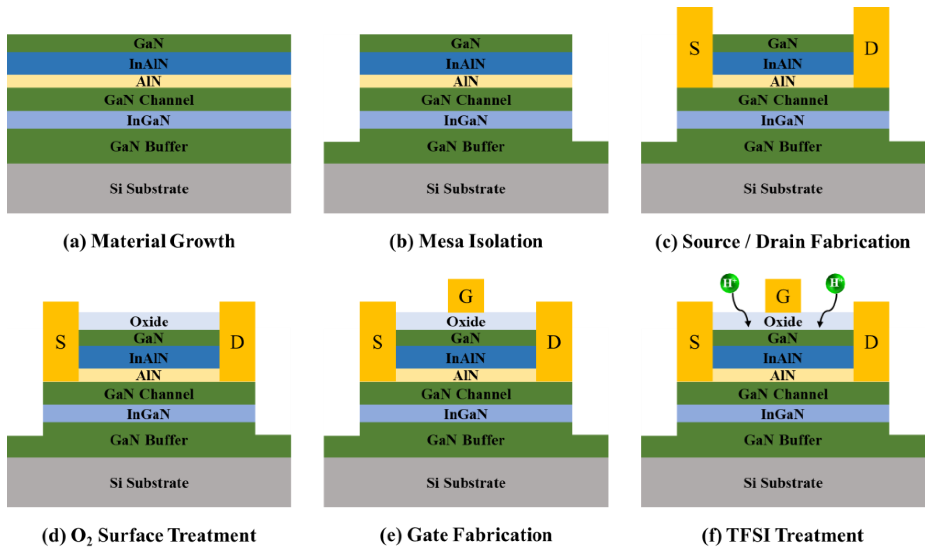
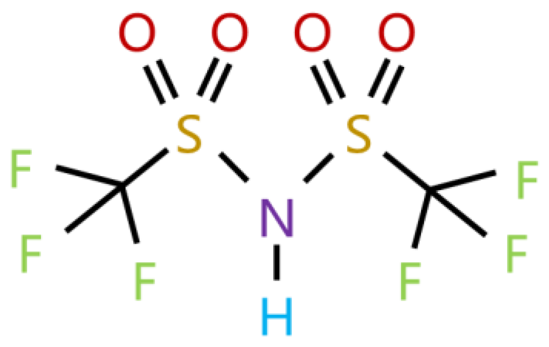
:1. Introduction
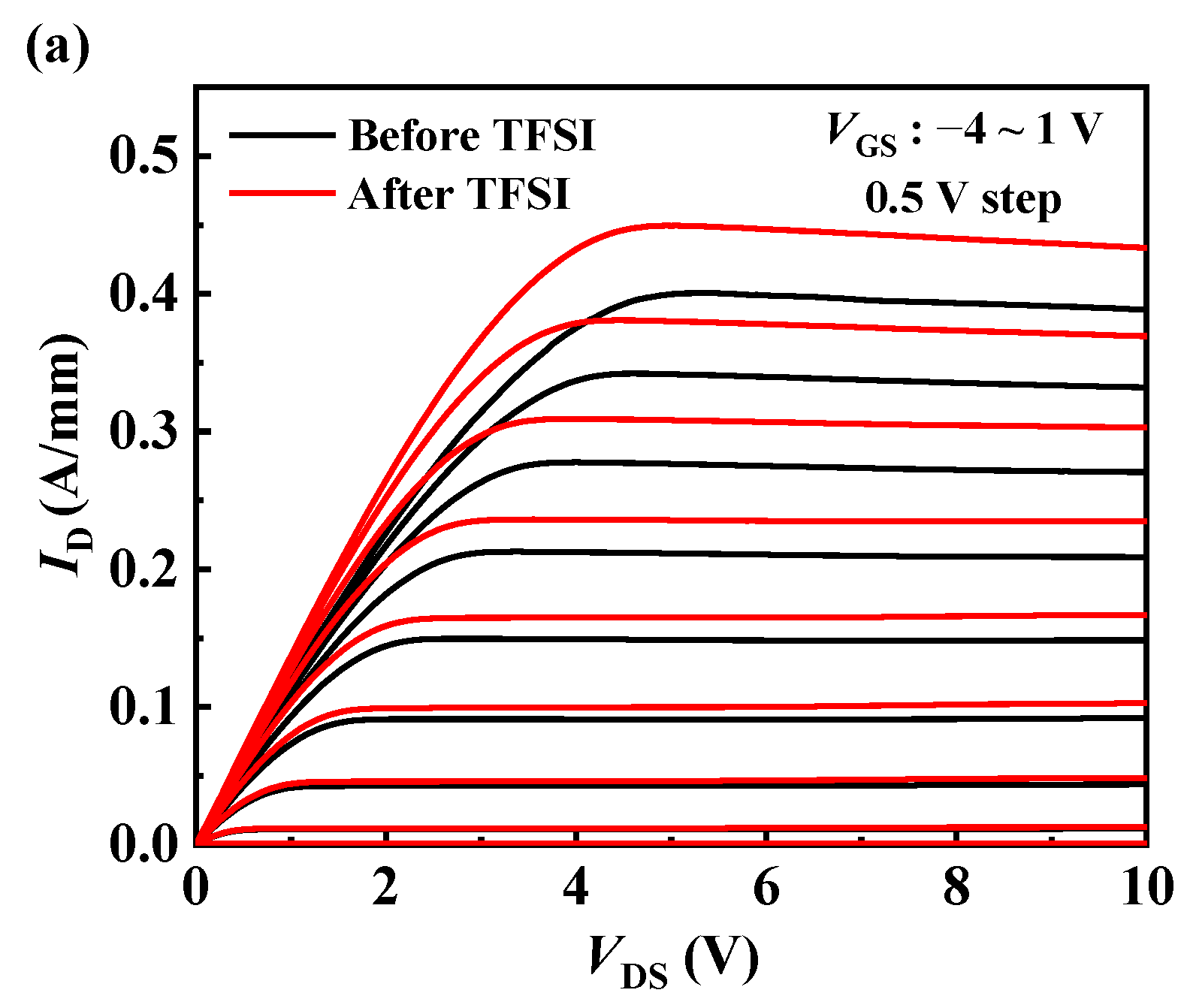
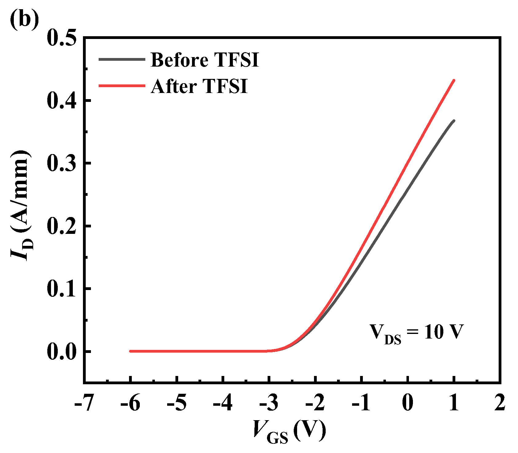
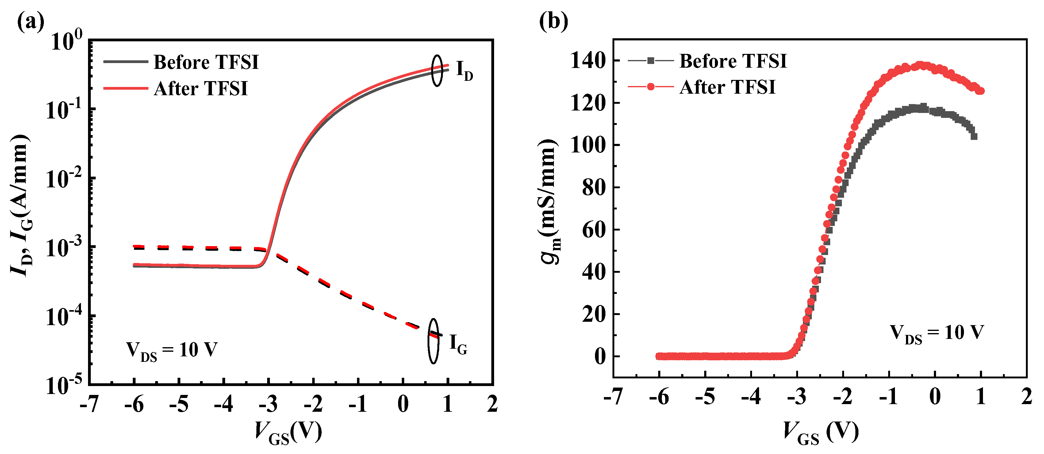
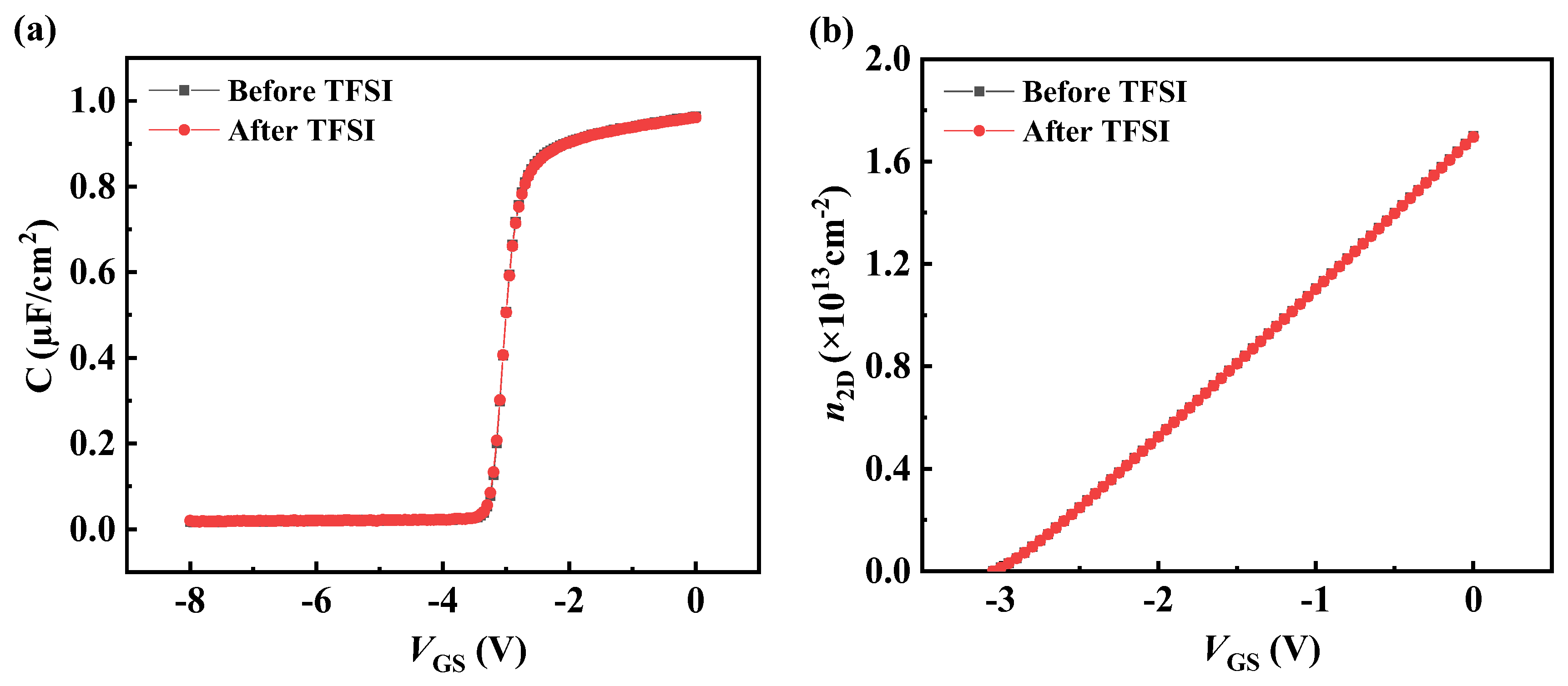
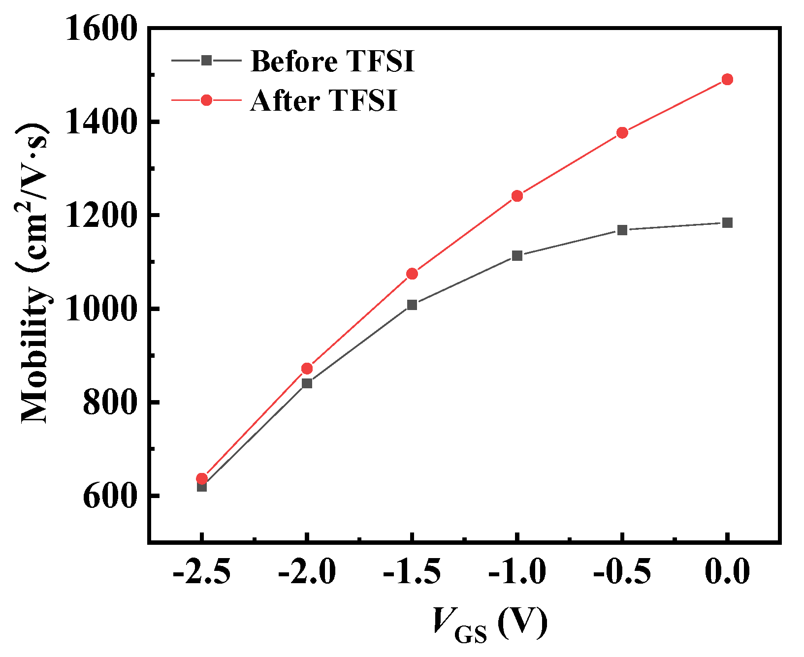
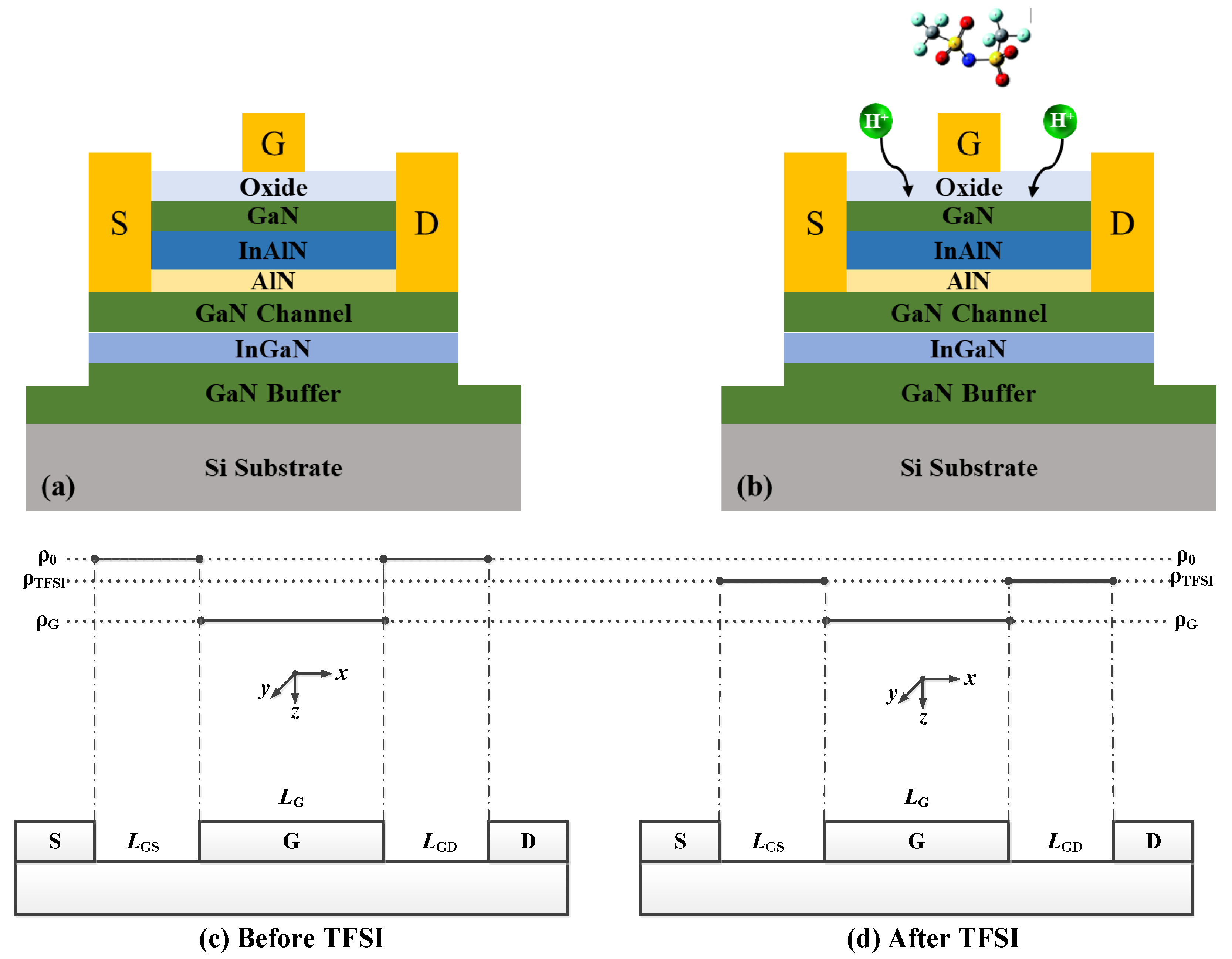
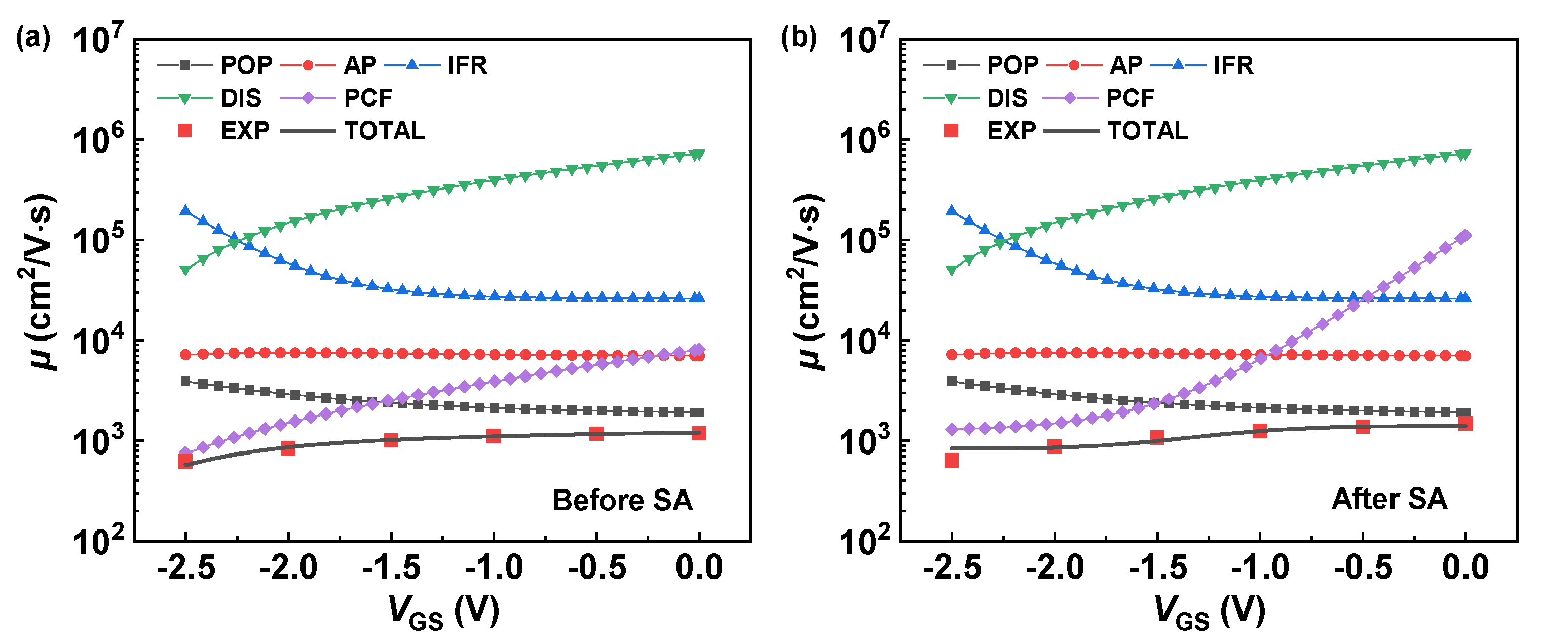
2. Results
3. Conclusions
Author Contributions
Funding
Institutional Review Board Statement
Informed Consent Statement
Data Availability Statement
Conflicts of Interest
References
- Selvaraj, S.L.; Watanabe, A.; Wakejima, A.; Egawa, T. 1.4-kV Breakdown Voltage for AlGaN/GaN High-Electron-Mobility Transistors on Silicon Substrate. IEEE Electron Device Lett. 2012, 33, 1375–1377. [Google Scholar] [CrossRef]
- Lu, B.; Palacios, T. High Breakdown (>1500 V) AlGaN/GaN HEMTs by Substrate-Transfer Technology. IEEE Electron Device Lett. 2010, 31, 951–953. [Google Scholar] [CrossRef]
- Cui1, P.; Mercante1, A.; Lin, G.; Zhang1, J.; Yao, P.; Prather, D.W.; Zeng, Y. High-performance InAlN/GaN HEMTs on silicon substrate with high fT × Lg. Appl. Phys. Express 2019, 12, 104001. [Google Scholar] [CrossRef]
- Mishra, U.K.; Shen, L.; Kazior, T.E.; Wu, Y.F. GaN-Based RF Power Devices and Amplifiers. Proc. IEEE 2008, 96, 287–305. [Google Scholar] [CrossRef]
- Ťapajna, M.; Hilt, O.; Bahat-Treidel, E.; Würfl, J.; Kuzmík, J. Gate Reliability Investigation in Normally-Off p-Type-GaN Cap/AlGaN/GaN HEMTs Under Forward Bias Stress. IEEE Electron Device Lett. 2016, 37, 385–388. [Google Scholar] [CrossRef]
- Kuzmik, J.; Kostopoulos, A.; Konstantinidis, G.; Carlin, J.-F.; Georgakilas, A.; Pogany, D. InAlN/GaN HEMTs: A first insight into technological optimization. IEEE Trans. Electron Devices 2006, 53, 422–426. [Google Scholar] [CrossRef]
- Wang, R.; Saunier, P.; Tang, Y.; Fang, T.; Gao, X.; Guo, S.; Snider, G.; Fay, P.; Jena, D.; Xing, H. Enhancement-Mode InAlN/AlN/GaN HEMTs with 10−12 A/mm Leakage Current and 1012 on/off Current Ratio. IEEE Electron Device Lett. 2011, 32, 309–311. [Google Scholar] [CrossRef]
- Lee, H.; Piedra, D.; Sun, M.; Gao, X.; Guo, S.; Palacios, T. 3000-V 4.3-mΩ·cm2 InAlN/GaN MOSHEMTs with AlGaN Back Barrier. IEEE Electron Device Lett. 2012, 33, 982–984. [Google Scholar] [CrossRef]
- Lee, D.S.; Gao, X.; Guo, S.; Kopp, D.; Fay, P.; Palacios, T. 300-GHz InAlN/GaN HEMTs with InGaN Back Barrier. IEEE Electron Device Lett. 2011, 32, 1525–1527. [Google Scholar] [CrossRef]
- Li, L.; Nomoto, K.; Pan, M.; Li, W.; Hickman, A.; Miller, J.; Lee, K.; Hu, Z.; Bader, S.J.; Lee, S.M.; et al. GaN HEMTs on Si with Regrown Contacts and Cutoff/Maximum Oscillation Frequencies of 250/204 GHz. IEEE Electron Device Lett. 2020, 41, 689–692. [Google Scholar] [CrossRef]
- Yue, Y.; Hu, Z.; Guo, J.; Sensale-Rodriguez, B.; Li, G.; Wang, R.; Faria, F.; Fang, T.; Song, B.; Gao, X.; et al. InAlN/AlN/GaN HEMTs with Regrown Ohmic Contacts and fT of 370 GHz. IEEE Electron Device Lett. 2012, 33, 988–990. [Google Scholar] [CrossRef]
- Kuzmik, J. Power electronics on InAlN/(In)GaN: Prospect for a record performance. IEEE Electron Device Lett. 2001, 22, 510–512. [Google Scholar] [CrossRef]
- Kuzmik, J.; Pozzovivo, G.; Ostermaier, C.; Strasser, G.; Pogany, D.; Gornik, E.; Carlin, J.-F.; Gonschorek, M.; Feltin, E.; Grandjean, N. Analysis of degradation mechanisms in lattice-matched InAlN/GaN high-electron-mobility transistors. J. Appl. Phys. 2009, 106, 124503. [Google Scholar] [CrossRef]
- Wang, R.; Saunier, P.; Xing, X.; Lian, C.; Gao, X.; Guo, S.; Snider, G.; Fay, P.; Jena, D.; Xing, H. Gate-Recessed Enhancement-Mode InAlN/AlN/GaN HEMTs with 1.9-A/mm Drain Current Density and 800-mS/mm Transconductance. IEEE Electron Device Lett. 2010, 31, 1383–1385. [Google Scholar] [CrossRef]
- Medjdoub, F.; Carlin, J.-F.; Gonschorek, M.; Feltin, E.; Py, M.A.; Ducatteau, D.; Gaquiere, C.; Grandjean, N.; Kohn, E. Can InAlN/GaN be an alternative to high power/high temperature AlGaN/GaN devices? In Proceedings of the 2006 International Electron Devices Meeting, San Francisco, CA, USA, 11–13 December 2006; pp. 1–4. [Google Scholar]
- Wang, R.; Li, G.; Laboutin, O.; Cao, Y.; Johnson, W.; Snider, G.; Fay, P.; Jena, D.; Xing, H. 210-GHz InAlN/GaN HEMTs with Dielectric-Free Passivation. IEEE Electron Device Lett. 2011, 32, 892–894. [Google Scholar] [CrossRef]
- Medjdoub, F.; AlOmari, M.; Carlin, J.-F.; Gonschorek, M.; Feltin, E.; Py, M.A.; Grandjean, N.; Kohn, E. Barrier-Layer Scaling of InAlN/GaN HEMTs. IEEE Electron Device Lett. 2008, 29, 422–425. [Google Scholar] [CrossRef]
- Gonschorek, M.; Carlin, J.-F.; Feltin, E.; Py, M.A.; Grandjean, N. High electron mobility lattice-matched AlInN/GaN field-effect transistor heterostructures. Appl. Phys. Lett. 2006, 89, 062106. [Google Scholar] [CrossRef]
- Medjdoub, F.; Carlin, J.-F.; Gonschorek, M.; Feltin, E.; Py, M.A.; Knez, M.; Troadec, D.; Gaquiere, C.; Chuvilin, A.; Kaiser, U.; et al. Barrier layer downscaling of InAIN/GaN HEMTs. In Proceedings of the 2007 65th Annual Device Research Conference, South Bend, IN, USA, 18–20 June 2007; pp. 109–110. [Google Scholar]
- Lee, D.S.; Chung, J.W.; Wang, H.; Gao, X.; Guo, S.; Fay, P.; Palacios, T. 245-GHz InAlN/GaN HEMTs with Oxygen Plasma Treatment. IEEE Electron Device Lett. 2011, 32, 755–757. [Google Scholar] [CrossRef]
- Cui, P.; Zhang, J.; Yang, T.-Y.; Chen, H.; Zhao, H.; Lin, G.; Wei, L.; Xiao, J.Q.; Chueh, Y.-L.; Zeng, Y. Effects of N2O surface treatment on the electrical properties of the InAlN/GaN high electron mobility transistors. J. Phys. D Appl. Phys. 2020, 53, 065103. [Google Scholar] [CrossRef]
- Ganguly, S.; Verma, J.; Hu, Z.Y.; Xing, H.L.; Jena, D. Performance enhancement of InAIN/GaN HEMTs by KOH surface treatment. Appl. Phys. Express 2014, 7, 034102. [Google Scholar] [CrossRef]
- Song, X.; Gu, G.; Dun, S.; Lü, Y.; Han, T.; Wang, Y.; Xu, P.; Feng, Z. DC and RF characteristics of enhancement-mode InAlN/GaN HEMT with fluorine treatment. J. Semicond. 2014, 35, 044002. [Google Scholar] [CrossRef]
- Cui, P.; Yang, T.-Y.; Zhang, J.; Chueh, Y.-L.; Zeng, Y. Improved On/Off Current Ratio and Linearity of InAlN/GaN HEMTs with N2O Surface Treatment for Radio Frequency Application. ECS J. Solid State Sci. Technol. 2021, 10, 065013. [Google Scholar] [CrossRef]
- Lin, G.; Zhao, M.-Q.; Jia, M.; Cui, P.; Zhao, H.; Zhang, J.; Gundlach, L.; Liu, X.; Johnson, A.T.C.; Zeng, Y. Improving the electrical performance of monolayer top-gated MoS2 transistors by post bis(trifluoromethane) sulfonamide treatment. J. Phys. D: Appl. Phys. 2020, 53, 415106. [Google Scholar] [CrossRef]
- Zeng, Y.; Khandelwal, S.; Shariar, K.F.; Wang, Z.; Lin, G.; Cheng, Q.; Cui, P.; Opila, R.; Balakrishnan, G.; Addamane, S.; et al. InAs FinFETs Performance Enhancement by Superacid Surface Treatment. IEEE Trans. Electron Devices 2019, 66, 1856–1861. [Google Scholar] [CrossRef]
- Amani, M.; Lien, D.-H.; Kiriya, D.; Xiao, J.; Azcatl, A.; Noh, J.; Madhvapathy, S.R.; Addou, R.; Kc, S.; Dubey, M.; et al. Near-unity photoluminescence quantum yield in MoS2. Science 2015, 350, 1065–1068. [Google Scholar] [CrossRef] [PubMed] [Green Version]
- Hirakawa, K.; Sakaki, H. Mobility of the two-dimensional electron gas at selectively doped n-type AlxGa1-xAs/GaAs heterojunctions with controlled electron concentrations. Phys. Rev. B 1986, 33, 8291–8303. [Google Scholar] [CrossRef] [PubMed]
- Gurusinghe, M.N.; Davidsson, S.K.; Andersson, T.G. Two-dimensional electron mobility limitation mechanisms in AlxGa1−xN/GaN heterostructures. Phys. Rev. B 2005, 72, 045316. [Google Scholar] [CrossRef]
- Luan, C.; Lin, Z.; Lv, Y.; Zhao, J.; Wang, Y.; Chen, H.; Wang, Z. Theoretical model of the polarization Coulomb field scattering in strained AlGaN/AlN/GaN heterostructure field-effect transistors. J. Appl. Phys. 2014, 116, 044507. [Google Scholar] [CrossRef]
- Shariar, K.F.; Lin, G.; Wang, Z.; Cui, P.; Zhang, J.; Opila, R.; Zeng, Y. Effect of bistrifluoromethane sulfonimide treatment on nickel/InAs contacts. Appl. Phys. A 2019, 125, 429. [Google Scholar] [CrossRef]
- Anwar, A.F.M.; Webster, R.T.; Smith, K.V. Bias induced strain in AlGaN/GaN heterojunction field effect transistors and its implications. Appl. Phys. Lett. 2006, 88, 203510. [Google Scholar] [CrossRef]
- Yang, M.; Lin, Z.; Zhao, J.; Cui, P.; Fu, C.; Lv, Y.; Feng, Z. Effect of Polarization Coulomb Field Scattering on Parasitic Source Access Resistance and Extrinsic Trans-conductance in AlGaN/GaN Heterostructure FETs. IEEE Trans. Electron Devices 2016, 63, 1471–1477. [Google Scholar] [CrossRef]
- Cui, P.; Mo, J.; Fu, C.; Lv, Y.; Liu, H.; Cheng, A.; Luan, C.; Zhou, Y.; Dai, G.; Lin, Z.; et al. Effect of Different Gate Lengths on Polarization Coulomb Field Scattering Potential in AlGaN/GaN Hetero-structure Field-Effect Transistors. Sci. Rep. 2018, 8, 9036. [Google Scholar] [CrossRef] [PubMed]
- Cui, P.; Liu, H.; Lin, W.; Lin, Z.; Cheng, A.; Yang, M.; Liu, Y.; Fu, C.; Lv, Y.; Luan, C.; et al. Influence of Different Gate Biases and Gate Lengths on Parasitic Source Access Resistance in AlGaN/GaN Het-erostructure FETs. IEEE Trans. Electron Devices 2017, 64, 1038–1044. [Google Scholar] [CrossRef]


Publisher’s Note: MDPI stays neutral with regard to jurisdictional claims in published maps and institutional affiliations. |
© 2022 by the authors. Licensee MDPI, Basel, Switzerland. This article is an open access article distributed under the terms and conditions of the Creative Commons Attribution (CC BY) license (https://creativecommons.org/licenses/by/4.0/).
Share and Cite
Chen, S.; Cui, P.; Xu, M.; Lin, Z.; Xu, X.; Zeng, Y.; Han, J. Improved Electrical Performance of InAlN/GaN High Electron Mobility Transistors with Post Bis(trifluoromethane) Sulfonamide Treatment. Crystals 2022, 12, 1521. https://doi.org/10.3390/cryst12111521
Chen S, Cui P, Xu M, Lin Z, Xu X, Zeng Y, Han J. Improved Electrical Performance of InAlN/GaN High Electron Mobility Transistors with Post Bis(trifluoromethane) Sulfonamide Treatment. Crystals. 2022; 12(11):1521. https://doi.org/10.3390/cryst12111521
Chicago/Turabian StyleChen, Siheng, Peng Cui, Mingsheng Xu, Zhaojun Lin, Xiangang Xu, Yuping Zeng, and Jisheng Han. 2022. "Improved Electrical Performance of InAlN/GaN High Electron Mobility Transistors with Post Bis(trifluoromethane) Sulfonamide Treatment" Crystals 12, no. 11: 1521. https://doi.org/10.3390/cryst12111521