Review

Research Progress in Capping Diamond Growth on GaN HEMT: A Review

1
Institute of Novel Semiconductors, Shandong University, Jinan 250100, China
2
The State Key Laboratory of Crystal Materials, Shandong University, Jinan 250100, China
3
School of Microelectronics, Shandong University, Jinan 250100, China
*
Authors to whom correspondence should be addressed.
Crystals 2023, 13(3), 500; https://doi.org/10.3390/cryst13030500
Submission received: 23 January 2023 / Revised: 3 March 2023 / Accepted: 7 March 2023 / Published: 14 March 2023
(This article belongs to the Special Issue Wide-Bandgap Semiconductors)

Abstract

:
With the increased power density of gallium nitride (GaN) high electron mobility transistors (HEMTs), effective cooling is required to eliminate the self-heating effect. Incorporating diamond into GaN HEMT is an alternative way to dissipate the heat generated from the active region. In this review, the four main approaches for the integration of diamond and GaN are briefly reviewed, including bonding the GaN wafer and diamond wafer together, depositing diamond as a heat-dissipation layer on the GaN epitaxial layer or HEMTs, and the epitaxial growth of GaN on the diamond substrate. Due to the large lattice mismatch and thermal mismatch, as well as the crystal structure differences between diamond and GaN, all above works face some problems and challenges. Moreover, the review is focused on the state-of-art of polycrystalline or nanocrystalline diamond (NCD) passivation layers on the topside of GaN HEMTs, including the nucleation and growth of the diamond on GaN HEMTs, structure and interface analysis, and thermal characterization, as well as electrical performance of GaN HEMTs after diamond film growth. Upon comparing three different nucleation methods of diamond on GaN, electrostatic seeding is the most commonly used pretreatment method to enhance the nucleation density. NCDs are usually grown at lower temperatures (600–800 °C) on GaN HEMTs, and the methods of “gate after growth” and selective area growth are emphasized. The influence of interface quality on the heat dissipation of capped diamond on GaN is analyzed. We consider that effectively reducing the thermal boundary resistance, improving the regional quality at the interface, and optimizing the stress–strain state are needed to improve the heat-spreading performance and stability of GaN HEMTs. NCD-capped GaN HEMTs exhibit more than a 20% lower operating temperature, and the current density is also improved, which shows good application potential. Furthermore, the existing problems and challenges have also been discussed. The nucleation and growth characteristics of diamond itself and the integration of diamond and GaN HEMT are discussed together, which can more completely explain the thermal diffusion effect of diamond for GaN HEMT and the corresponding technical problems.

1. Introduction

As a representative third-generation semiconductor material, GaN has excellent properties, such as a large band gap, high breakdown voltage, and high electron saturation drift velocity [1,2,3,4]. The GaN-based devices exhibit high-power density and conversion efficiency. In the applications of 5G communication and radar, GaN HEMTs can provide more than 10 times higher power density than existing Si technology, so they have great application in high-frequency, high-power microwave, millimeter wave devices and circuits [5]. However, due to this high operating power density, the heat effect in the active region of the chip accumulates, and the heat flux of the local hot spot can reach 10 kW·cm2, while the volumetric heat generation under the package exceeds 100 W·cm−3 [6]. The reliability and stability of GaN HEMT devices are seriously challenged with conventional thermal management. As the highest thermal conductivity material in nature, diamond is a good thermal management choice. Early simulations and modeling showed that the passive thermal extraction by directly fabricating it with diamond could dramatically reduce junction temperatures by 25–50%. In recent years, great experimental progress has been made [7,8,9]. Apart from GaN HEMTs, some researchers have also studied the heat-dissipation effect of diamond on LED [10,11], which is beyond the scope of the review.
In this paper, several methods to enhance the heat dissipation of GaN HEMTs by using diamond are briefly introduced. The integration process of capped-diamond on GaN HEMTs is mainly described, including the nucleation and growth of diamond on GaN, the analysis and optimization of interface quality, and the improvement of the thermal and electrical properties of devices after diamond layer deposition. In this method, the nucleation of diamond on GaN, keeping a high-quality interface, high stress–strain, and thermal boundary resistance are the main difficulties and breakthrough directions. This paper describes in detail the potential and technical challenges of this approach and discusses its advantages and disadvantages.

2. Heat Dissipation Technology of GaN HEMTs with Diamond

The well-established technology for AlGaN/GaN heterojunction materials was grown on sapphire, high-resistance silicon and silicon carbide (SiC) substrates [12,13,14]. Up to now, SiC has been the mainstream substrate for high-power applications due to the highest thermal conductivity and least lattice mismatch of these three. The currently fielded and commercially available HEMTs are operating at only 5–6 W/mm, which is far lower than the experimental 42 W/mm [15]. Diamond has more prominent application advantages over other materials and is expected to significantly improve the self-heating effect of the devices and solve the problem of the deterioration of device performance under high-frequency and high-power operating conditions, as listed in Table 1. However, there are still great mismatches between diamond and GaN, mainly including lattice constants, thermal expansion coefficients (TECs), and crystalline structures. Thus, the integration of diamond and GaN also faces great technical challenges.
How to use diamond as heat sinks or substrates for GaN-based power devices has been reported in a variety of technical methods, mainly including bonding diamond to GaN wafers or HEMT devices, the epitaxial growth of GaN on single crystal diamond substrates, and the growth of nanocrystalline or polycrystalline diamond on the topside or backside of GaN or HEMT devices, as shown in Figure 1.

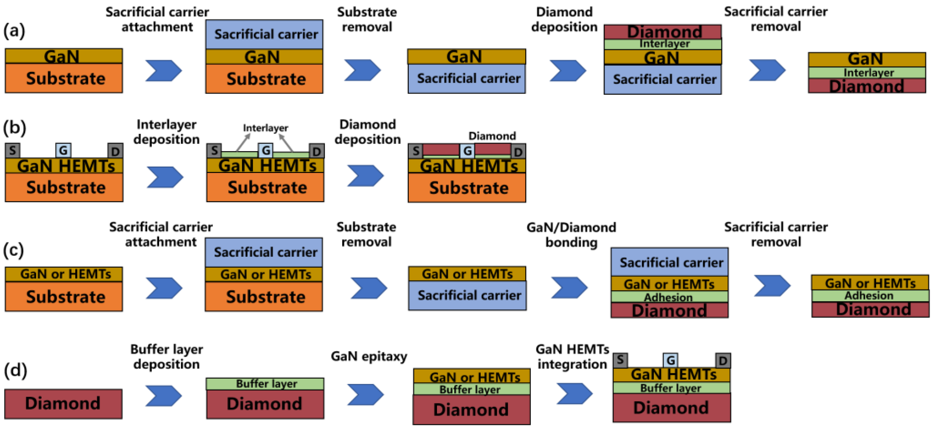
2.1. Bonding Diamond to GaN Wafers or HEMT Devices

The GaN/diamond bonding method based on transfer technology is a flexible process, which can realize the simultaneous preparation of the GaN epitaxial layer and diamond substrate and effectively ensure high thermal conductivity of the diamond substrate [6]. In this method, GaN epitaxial materials or devices are first grown on Si and other substrates, and the upper surface is bonded with a suitable sacrificial carrier to remove the original substrate, and then, the lower surface of the epitaxial material is combined with the diamond heat-dissipation layer at the atomic level. Finally, the sacrificial carrier is removed to obtain GaN epitaxial materials or devices based on diamond substrates. At present, this technical method has been able to adopt a more mature form of low-temperature bonding reported by the BAE Systems and Nanjing Electronic Devices Institute (NEDI) [20,21]. The output power density of GaN devices on diamond substrates obtained by BAE Systems is 3.6 times that of traditional SiC substrates, reaching 11 W/mm [20,22]. However, this method has great requirements for the quality of the bonding interface layer, such as parallelism, deformation, and surface roughness. High-precision machining on the bonding surface of the large-size diamond substrate and GaN epitaxial layer is necessary. In addition, further optimizing the relevant parameters, such as the thermal conductivity, thickness, and bonding process of the bonding layer to reduce the boundary thermal resistance between the heterogeneous layers, should be carried out systematically.

2.2. Epitaxial Growth of GaN on the Diamond Substrate

There is a lasting interest in the method of direct epitaxial GaN or HEMTs on the diamond substrate [23,24]. Representative research groups include Swiss EPFL [25], Element 6, and Japanese NTT teams [26,27,28]. A polycrystalline diamond substrate has been tried, which led to serious deterioration of the GaN film, even to amorphous growth, so it is far from the device demand. With the development of single crystal growth, the mainstream application substrate of this method turns to single crystal diamond. The focus is on the use of single crystal diamonds with different orientations, such as (110), (111), and (100), etc. In 2011, Hriama et al. from NTT Corporation, Japan, reported GaN-based HEMTs with a max power output of 220 mA/mm on the (111) diamond substrate. The two-dimensional electron gas mobility (2DEG) and sheet carrier density were 730 cm2/Vs and 1.0 × 1013 cm−2 at room temperature, respectively. The current gain cut-off frequency and the maximum oscillation frequency are 3 GHz and 7 GHz, respectively [27]. Subsequently, in 2012, the same group updated the new result. At 1 GHz, the output power density is 2.13 W/mm, the gain is 28 dB, the power added efficiency is 46%, and the current gain cut-off frequency and the highest oscillation frequency are 5 GHz and 18 GHz, respectively [28]. This is the first report on the RF characteristics of HEMT devices made of AlGaN/GaN heterostructure material grown epitaxially on a diamond substrate. While successfully preparing heteroepitaxial materials and devices on single crystal diamond substrates, the out-power density is near half that of GaN-on-SiC HEMTs. This implies that this approach faces great technical challenges originating from the large differences in lattice constants and thermal expansion coefficients and the structural differences between diamond and GaN. Therefore, nowadays, the core task is to overcome the bottleneck of direct epitaxy GaN materials or devices on the diamond substrate [29,30].

2.3. Diamond Epitaxially Grown on GaN Substrate or HEMTs

The epitaxial growth of diamond on GaN is a relatively mature method. It can also be divided into the direct growth of diamond on the back of GaN epitaxial layers or HEMT devices and the direct deposition of a polycrystalline or nanocrystalline diamond heat dissipation layer on the top of GaN HEMTs. However, it is difficult to grow a single crystal phase even on some cubic structure substrates, since diamond only nucleates on the substrate of some potential carbide-forming materials. Therefore, the diamond deposited on GaN only forms a polycrystalline or nanocrystalline phase. The direct deposition of diamond on a GaN epitaxial layer has the advantage of being as close as possible to the heat-generation position of HEMTs, which is obviously helpful to the heat dissipation [31].
The chemical vapor deposition (CVD) process is the most suited technique for large-area thin films, which involves chemical reaction inside a gas-phase, as well as deposition onto a substrate surface. William G Eversole proposed a CVD growth method in 1961 [32]. Angus et al. [33] became the first group who could synthesize diamond via a CVD process. Based on the sort of energy supply, the activation can be generated by microwave (MW), radio frequency (RF), laser-induced (LI), direct current (DC), hot filament (HF), and chemical activation (CA) [34]. Among the above-mentioned, the diamond prepared via the microwave plasma chemical vapor deposition (MPCVD) method has the advantages of a stable growth process, high purity, large-area film preparation, and high thermal conductivity. Therefore, it is widely used as a heat-dissipation material under ultra-high heat flow density conditions, such as radar components.
Figure 2 is the photo of directly depositing polycrystalline or nanocrystalline diamond at the topside of GaN HEMTs. The capping diamond concept was initially proposed in 1991 [35]. This method being applied to GaN HEMTs started relatively late, and diamond was directly deposited into the channel of the devices, closer to the active region. Many researchers used the simulation method to study the heat dissipation effect of diamond as important reference information.
From the results of Figure 3 and Table 2, capped diamond can effectively suppress the self-heating effect and improve the electrical performance of GaN HEMTs. Compared with those of the conventional GaN-on-Si, gm and fT are increased by 14% and 17%, respectively [36]. Zhang et al. conducted a series of simulations on the cooling effect of capped diamond on GaN HEMTs. For the 12-finger model with a 20 µm gate pitch gate distance and gate power density of 6 W/mm, a 20 µm layer of capped diamond could reduce the junction temperature by 12.1% for GaN-on-diamond HEMTs and by 25.3% for GaN-on-SiC HEMTs [37]. They simulated the heat-spreading effect of the film thickness and diamond anisotropy on the pulsed-operated GaN HEMTs [38]. The results showed that the 2 μm-thick diamond film can effectively reduce the dynamic steady-state peak junction temperature to 14.7% when the device works at a duty cycle of 2.5%, a pulse period of 200 μs, and a peak power density of 19.58 W/mm. Because the peak power density is inversely proportional to the duty cycle, the intensive heating decreases as the duty cycle increases. In addition, the device operating with a smaller pulse period has a narrower pulse ON-state time window, so the heat-accumulation effect becomes weaker. Therefore, the duty cycle and pulse period under this condition will also make the cooling effect of the capped diamond more profound. In addition, the above group also tried to integrate the capped diamond with the manifold microchannel cooling (EMMC) GaN HEMTs [39]. The 5 μm-thick diamond layer can increase the drain current of the device by 10.5%, and the self-heating effect can be neglected for a 100 ns pulse width at a 1 V gate and 20 V drain voltage. The new EMMC device structure complements the capped diamond to reduce the junction thermal-spreading resistance and expand the near-junction cooling scheme. In 2017, Zhou et al. [40] extensively studied the heat-spreading benefit of polycrystalline diamond layers with different thin film thicknesses, in which polycrystalline diamond films exhibited strong layer-thickness dependence. Use of the experimental KDia and thermal boundary resistance values in the device simulation predicted that the peak temperature was reduced by up to 15% when the source-drain opening of the GaN HEMT was overgrown with PCD. The simulation and experiment provided guidance for the heat-spreading limit of this technical method. The integration of diamond and GaN provides positive results from above-simulated modeling. However, the experimental results still show many technical problems needed to be further solved and will be further discussed in detail in Section 6.
Using the method of depositing diamond on the back of the GaN epitaxial layer, Group 4 Laps from the United States is the main research group [23,41,42,43]. They studied the decomposition mechanism of GaN in the high-temperature gas environment and the influence of the diamond deposition process on GaN HEMT devices. They first proposed three important conclusions: (1) GaN can be exposed at higher temperature for a long time without detecting changes in electrical properties, (2) the thermal mismatch between the GaN epitaxial layer and the diamond film does not affect the device [42], and (3) diamond can be deposited on Si-based GaN [44]. The group of Obo and Sugino deposited diamond films on the (0001)-oriented GaN epitaxial layer and realized the growth of directional heteroepitaxial isolated diamond crystals [45]. However, due to the low nucleation density, a continuous diamond film was not formed. This is the first attempt to deposit diamond film on hexagonal GaN. In 2011, D. Francis and Tyhach M of Group 4 Labs completed a 4-inch GaN HEMT on a 100 μm-thick diamond substrate [46], which is the largest diameter for a GaN wafer on a diamond substrate ever reported. At present, the optimal RF performance of AlGaN/GaN HEMTs can obtain a power density of 7.9 W/mm at 10 GHz and a 40 V bias voltage, and the PAE can reach 46% [47].
However, subjecting GaN to the harsh diamond-growth environment, which is the hydrogen-containing high-temperature condition, leads to performance degradation of GaN and related devices. The coping strategy is to deposit a dielectric layer on the backside of GaN epitaxial layer or on the topside of the device and then use chemical vapor deposition (CVD) to grow the diamond film heat-dissipation layer [48,49,50]. Obviously, the introduction of the interlayer will increase the effective thermal boundary resistance (TBReff), limiting the heat dissipation performance of diamond for the GaN-based devices. Secondly, there is a nucleation layer during the diamond growth process, which will lead to enhanced phonon scattering due to the high density of different orientation nanocrystalline diamond grains, grain boundaries, impurities, and defects. Thirdly, because of the easy degradation of GaN during diamond deposition, a lower temperature condition is needed. Therefore, how to ensure the quality of diamond at low temperature is also an important problem. Table 3 shows the advantages and disadvantages of different integration methods.
The method of depositing capped diamond on GaN HEMTs is the focus of this review. All works listed in this review were undertaken to solve the problems, including the degradation of III-nitride layers in the harsh CVD environment, thermal stress caused by the mismatch of the thermal expansion coefficient of the materials, and reducing the thermal boundary resistance of GaN/interlayer/diamond [52]. Any change in the stress–strain state in AlGaN/GaN heterostructures, especially in the AlGaN barrier layer, will have a great influence on 2DEG characteristics [53]. Researchers try to find a way to achieve the balance between the properties of GaN HEMTs and the deposition conditions of diamond. Thus, the subsequent section focuses on the nucleation and growth characteristics of diamond, the analysis of the GaN/diamond interface, and the thermal and electrical properties of GaN HEMTs.

3. Nucleation of Diamond

GaN is very stable in an air environment and begins to decompose when it is heated to 1300 °C. However, it becomes very unstable in a high-temperature hydrogen plasma environment and is prone to decomposition and deterioration, which will lead to a large number of new defects and seriously affect the electrical properties of AlGaN/GaN [52,54]. From the study of Akinori Koukitu et al., H2 promotes the decomposition of GaN in the high-temperature environment. H and N atoms combine to form NH3, and the increased temperature will also lead to Ga and H atoms combining and even cause the formation of Ga droplets [55]. The addition of N2 can make the balance of the GaN decomposition reaction shift to the left, inhibit the decomposition of GaN, and enhance the stability of GaN. In addition, forming a dense diamond nucleation layer on the surface of GaN in a short time can play an effective role in protecting GaN.
Nucleation is a key process for the growth of diamond films. Spontaneously nucleation on heterogeneous substrates is difficult. This is mainly because the high surface energy of diamond. Rapid nucleation (a few minutes commonly) is a necessary condition for the deposition of high-quality diamond films. The characteristics of the substrate, such as surface defects, surface energy, surface diffusion and bulk diffusion of atoms, and chemical reactivity [56,57], affect the diamond nucleation process. Especially, a GaN substrate, which has a large lattice mismatch and thermal expansion mismatch with diamond, puts forward some difficult requirements for diamond nucleation. The temperature of the substrate also affects the diamond nucleation process. Considering the quality and rate of diamond nucleation and the thermal stability of GaN HEMT, researchers regard ~600 °C as a more suitable nucleation temperature. A. Kromka et al. introduced the thermodynamic and kinetic conditions of diamond nucleation in detail in his work [58]. To achieve high-quality nucleation efficiency, adopting some technical methods of assisted nucleation is necessary. Substrate pretreatment becomes a commonly used method, mainly including ultrasonic treatment with a diamond powder suspension, applying bias voltage to enhance nucleation and electrostatic seeding on the substrate surface by diamond nanoparticles. The above methods are for technical approaches to the growth of diamond on GaN layers.

3.1. Nucleation through Ultrasonic Particle Treatment

Ultrasonic pretreatment in a diamond powder suspension is performed to form scratches on the substrate surface or attach diamond particles to the substrate as nucleation sites [59]. The liquid used for the suspension is mainly ethanol, acetone, and pure water, etc. [60]. This method is relatively simple to operate, because there is no excessive requirement for the substrate’s geometry, and no special deposition equipment is required. In the experiment by Mohapatra et al. [61], to enhance the density of diamond nucleation sites, the substrate was ultrasonically treated in a 2 μm-sized diamond powder suspension for 10 min, with subsequent cleaning with acetone and deionized water in an ultrasonic bath. Continuous diamond films with a high nucleation density were obtained. However, the core purpose of the ultrasonic pretreatment method is to damage the substrate surface and create residual diamond particles to increase the nucleation density, which makes the substrate damaged or roughened [56]. Therefore, it is limited to use in the subsequent experimental study of diamond film growth on GaN. Especially, for the technical method of directly depositing diamond on the top of GaN HEMTs, this pretreatment process is likely to cause damage to the AlGaN barrier layer and affect the further use of the devices. This method is not very suitable for this growth technique approach.

3.2. Bias Enhanced Nucleation

The use of a biased voltage in a CVD chamber to promote diamond nucleation is called Bias Enhanced Nucleation (BEN), which was first proposed by Yugo et al. [62]. Lifshitz et al. detailed described the bias-enhanced nucleation process and proposed the corresponding mechanism [63]. As mentioned above, Oba and Sugino have used bias enhanced nucleation prior to diamond deposition onto GaN materials in a microwave plasma chemical vapor deposition chamber [64]. However, they could not grow a continuous film due to the low nucleation density. In 2011, Alomari et al. reported a 0.5 μm-thick NCD film process on In0.17Al0.83N/GaN HEMTs via hot filament chemical vapor deposition at 750–800 °C [65]. After NCD deposition, the fT and fmax of the device were 4.2 and 5 GHz, respectively. Moreover, the DC characteristics were basically similar to those before deposition. However, the RF-tested device showed high gate leakage, probably due to the effect of the high-temperature and hydrogen-rich deposition environment on the gate dielectric and gate metal. In 2014, the NCD layer was increased to a 2.8 μm thickness [66].
BEN can greatly improve the nucleation site density before diamond growth, providing a prerequisite for the high-quality nanocrystalline diamond. The typical nucleation density achieved by BEN is in the order of 1010 cm−2. However, the BEN method also has some disadvantages, such as being only applicable to conductive substrates [56].

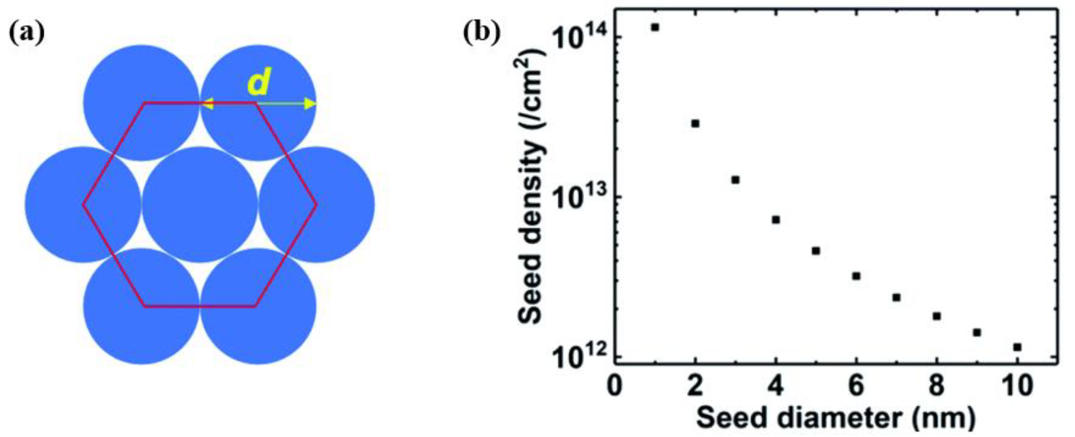
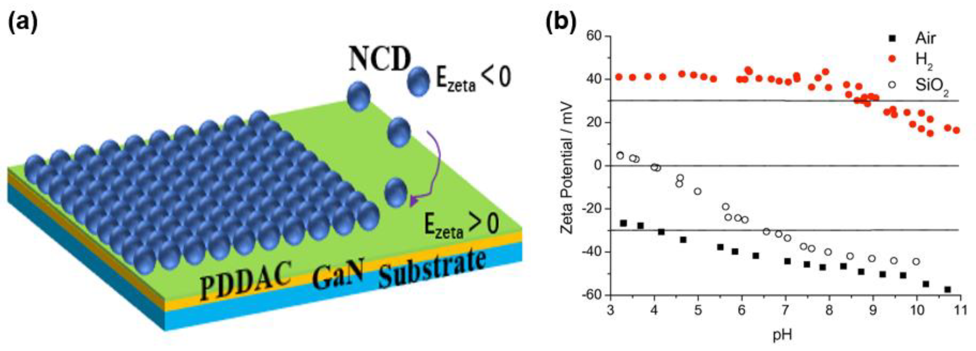
3.3. Electrostatic Seeding

At present, electrostatic seeding is the most widely used pretreatment method for enhancing the nucleation of polycrystalline diamond films [67]. The main process is to establish a heterogeneous charge difference between the substrate and the diamond powders and use electrostatic adsorption to realize the diamond powder seeding [68,69]. Specifically, by cleaning the substrate or directly coating a suitable polymer layer on the substrate surface, the nanodiamond powders with opposite potential are self-assembled on the substrate to form a uniform single-particle diamond powder layer. Figure 4 shows a schematic diagram of perfectly spherical seeds densely packed in hexagons and the theoretical maximum seeding density with different seed diameters. The preparation of a stable and uniform diamond colloidal suspension is one of the important prerequisites. Diamond is insoluble in water or any other solvent, which helps the corresponding diamond colloidal suspension form. The colloidal suspension stability is determined by the suspended particles’ potential, and it is generally believed that an absolute value of the ζ-potential more than 30 mV will create a good condition for forming a stable colloidal suspension [52]. It should be noted that the amount of nanodiamond particles added to the solvent is also the critical factor. Too few nanodiamond particles may not meet the high-density diamond particle seeding requirement. Too many nanodiamond particles will lead to a great increase in the collision probability between particles. This process will make the van der Waals forces between particles possible to overcome the repulsive potential caused by the surface charge and finally lead to agglomeration. In addition, the diamond particle size will also have a certain impact on the colloid stability [70]. Obtaining a uniform monodisperse colloidal suspension is an essential part; the colloid is conducive to improving the seeding quality and increase seeding density [69,71,72]. Smaller particles currently used for seeding treatment are produced via the detonation of unused or decommissioned explosives, and these diamond particles are called detonation nanodiamond (DND). In the process of producing nanodiamond via detonation, a large amount of sp2-phase carbon is formed, and it is precisely because this part of non-diamond carbon promotes the formation of large diamond particle agglomerates. The existence of agglomerates makes it difficult to obtain monodisperse diamond colloids. The methods of preparing monodisperse single nanodiamond particulates are mainly high-power ultrasonic treatment, stirred-media-milling method, and dispersant assisted dispersion. An in-depth discussion about preparing monodisperse nanodiamond colloids is beyond the scope of this review.
In 2007, Ozawa et al. obtained the first DND (4–5 nm sized particles) monodisperse colloidal suspension via a wet milling process using zirconia beads to help disperse diamond powders [73]. Due to the smaller gap between particles, the smaller diamond particles can effectively achieve a high seed density. Stehlik et al. used 2 nm DND as diamond seeds to obtain a seed density of up to 2.88 × 1013 cm−2 [74]. As mentioned above, the reason why a high seeding density can be formed on the substrate surface is that there is a certain potential difference between the substrate surface and the DND colloid. Changing the condition, such as the pH value and surface potential, can control this part of the potential difference. Figure 5 shows the ζ potential of a hydrogenated and oxidized diamond colloid solution measured over a wide range of pH values. Mandal et al. studied the potential changes in the Ga-face and N-face GaN with pH in detail [75]. Between pH 5.5 and 9, both showed a negative ζ potential, while the potential of N-face GaN showed a more negative ζ potential, which was mainly due to the larger concentration of adsorbed oxygen on the surface. Some researchers have also tried to change the surface potential ζ by covering a polymer layer on the substrate [76,77,78,79]. This polymer will undergo corrosion decomposition during the CVD heating process, leaving nanocrystalline diamond seeds on the substrate surface. Currently, the polymers commonly used are poly-diallyldimethylammonium chloride polymer (PDDAC), polystyrene sulfonic acid (PSS), and polyvinyl alcohol (PVA) etc., and the process adsorbed on the surface of the substrate particles or polymer mass is determined by the Sauerbrey equation. At present, this technology has been able to achieve selective seeding on the substrate and allow ND deposition matching complex 3D structures [58,68,76,78,80].
In addition, nucleation is also affected by process parameters. Too high pressure in the reaction chamber will lead to a decrease in the nucleation rate. An excessive substrate temperature and carbon concentration will make the quality of diamond films decrease. Otherwise, it will affect the uniformity of nucleation. Moreover, the material of the substrate will also have a significant impact on the nucleation process. This section aims to focus on the effect of pretreatment methods on nucleation, and the dependence on the temperature is slightly mentioned. Temperature is generally a key parameter of the nucleation by increasing the surface diffusion of atomic species. Many examples of enhanced nucleation with temperature were found with different deposition methods, and an optimum temperature has been found to exist at ~860 °C where the nucleation density reaches a maximum. Reactive species or molecules are physically (<900 °C) and chemically (>900 °C) adsorbed on the substrate surface. This leads to an abrupt change in the diffusion length at ~900 °C. When the temperature is close to 860 °C, the adhesion probability of the active species on the substrate surface increases [81]. The effect of substrate temperature on diamond nucleation can be obtained from this literature in detail [82,83,84].

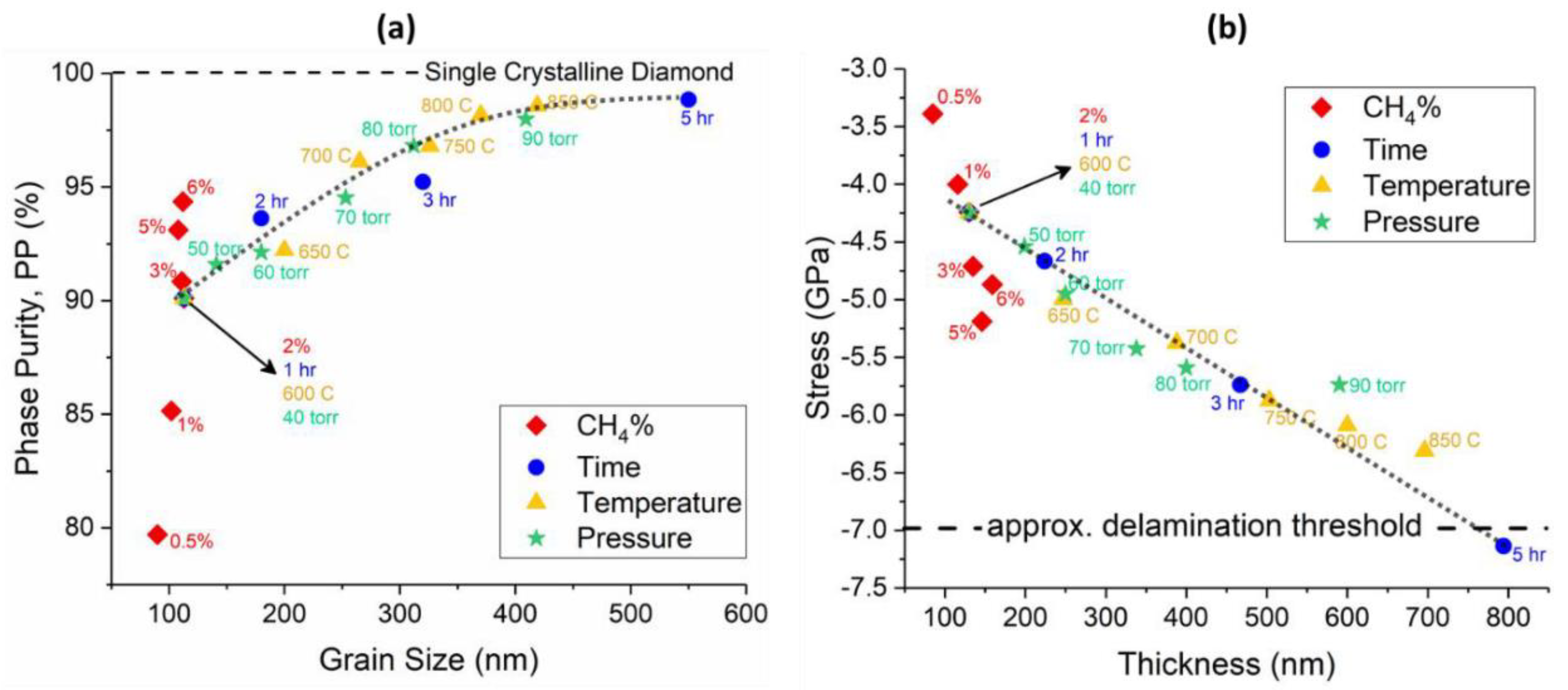
4. Growth of Polycrystalline or Nanocrystalline Diamond

The diamond deposition reaction mainly includes the following three main processes [85,86]:
CdH + H* → Cd* + H2
Cd* + H* → CdH
Cd* + CH3 = Cd-CH3
The first two equations represent the activation process of surface reaction sites for carbon deposition. Equation (3) indicates that the process of diamond deposition is the result of the interaction between the growth and etching of diamond. The percentage of surface open reaction sites is a key parameter to determine the growth rate, which is usually expressed by the fraction of reaction rates (k1/k2) [87]. The reaction rates of those equations can be described by A*exp(−Ea/RT), where the activation energy for k1 is 7.3 and is 0 kcal/mol for k2 [88,89,90]. In this process, under the action of microwaves, hydrogen is decomposed into H plasma, which can bombard the surface of the sample. Then, the chemical bonds on the substrate material surface can be opened, so as to provide dangling bonds for the free radicals of the carbon source to bind to the surface and help diamond growth. During this process, hydrogen plasma will also cause an etching effect on the substrate and improve the growth quality of diamond by etching the growth defects of the surface and amorphous carbon, graphite, and other phases [85]. According to a large number of experimental studies, setting different growth conditions can significantly affect the surface morphology, quality, and growth rate of polycrystalline diamond. These growth parameters mainly include the microwave power, pressure, temperature, gas system and proportion, and plasma conditions, etc. Higher power and gas pressure can effectively suppress the secondary nucleation of diamond, and a faster growth rate contributes to the formation of micron-crystalline diamond. On the contrary, if the secondary nucleation rate of diamond is enhanced by controlling the parameters, including a high substrate temperature, high methane concentration, and the addition of inert gas, the formation of nanocrystalline diamond will be promoted [87,91]. Moreover, in the atmosphere of Ar, nanocrystalline diamond and ultra-nanocrystalline diamond (UNCD) can be obtained by Ar ion bombardment. However, the existence of a large amount of Ar ions will lead to low diamond phase purity, that is, the ratio of sp3/sp2 is lower, which should be considered in the application for thermal diffusion [92,93].
In Figure 6, Seelmann-Eggebert et al. firstly explored the preparation of a diamond passivation layer on the GaN field effect transistor (FET) surface, optimized the growth of the protective layer, nucleation, and deposition process, and completed the deposition of 0.7 μm- and 2 μm-thickness diamond (sub-μm particle size) at 440 °C and 480 °C [94]. Although the diamond quality is poor and the heat dissipation effect is not good due to low-temperature growth conditions, it provides some guiding tips for the application of diamond to GaN devices for heat dissipation.
As is shown in Figure 7a,b, Alomari et al. successfully grew a 4.5 μm-thick nanocrystalline diamond layer on InAlN/GaN in a temperature range of 750 °C to 800 °C [95]. However, there are problems of poor current efficiency and ohmic contact degradation [65], which is because the device itself is not resistant to a high-temperature and hydrogen-rich environment. In 2011, Govindaraju et al. deposited an NCD layer on AlGaN/GaN HEMT via a low-temperature growth process (<350 °C) and found that this process will not cause damage to the metallization of the device [8]. However, under these low temperatures, the quality of the diamond film is relatively poor. Moreover, they considered that the metallization damage is a complex phenomenon, involving the solid-state reaction between the metal and the substrate. In addition, Goyal et al. directly deposited high-quality nanocrystalline diamond films on GaN substrates at low temperatures of 450–500 °C [96]. The grain size of crystalline diamond is in the range of 100–200 nm. The above study complements the experiment of depositing diamond on a GaN substrate at this temperature range and obtains better diamond quality and surface morphology. In 2012, M. J. Tadjer et al. proposed AlGaN/GaN HEMTs with high-quality nanocrystalline diamond heat-spreading layers (0.5 and 2 μm-thick) using a “diamond-before-gate” approach [97]. The nanocrystalline diamond film provided a high thermal conductivity path only 50 nm away from the gate, and the heat spreading effect was increased by 20%.
In 2019, Malakoutian et al. analyzed the method and path of growing polycrystalline diamond on N-GaN using Si3N4 as passivation layer in detail and summarized a relatively complete growth window of polycrystalline diamond on such substrates, in Figure 8, which provided a general guideline for related work [98]. Subsequently, the group used the existing growth parameters to successfully prepare a thin and dense nanocrystalline diamond layer with abrupt interface on a bare and Si3N4-coated N-polar GaN substrate and kept the growth rate at 0.18–0.25 μm/h with a uniform particle (140–180 nm) and thickness (180–250 nm). The next step will be expected to be further grown on large-sized wafers.
Selective area deposition has also been the focus of researchers. Compared with the overgrowth method, the selective area deposition process can avoid the deposition of diamond on the electrodes, eliminate the effect of electrode degradation, and omit the step of ICP etching to open the electrode position. Zou et al. deposited diamond films on patterned GaN substrates with a thin silicon nitride protective layer [99], which effectively prevented plasma-induced GaN decomposition and etching, eliminated film cracks and delamination, and obtained high-quality diamond films. In 2010, Babchenko et al. reported the approach of a photo-resistive polymer to pattern the diamond-seeding layer [100]. By combining reactive ion etching (i.e., dry process) and wet photo lithographical processing using two polymer layers, better processing technology for patterned diamond growth was achieved. Tibor Izak et al. used selective area in a three-layer sandwich structure (polymer/seeding layer/polymer) for diamond nucleation and growth on AlGaN/GaN heterostructures [80] to eliminate surface and metal contact damage (Ni, NiO, Ir, and IrO2) and suppress the spontaneous nucleation of diamond. Selective area growth is considered a possible and viable method that still needs improvements to avoid the uncertainty caused by the etching process after diamond deposition. Figure 7c shows a top-view SEM image of NCD grown on a GaN substrate via selective area deposition.

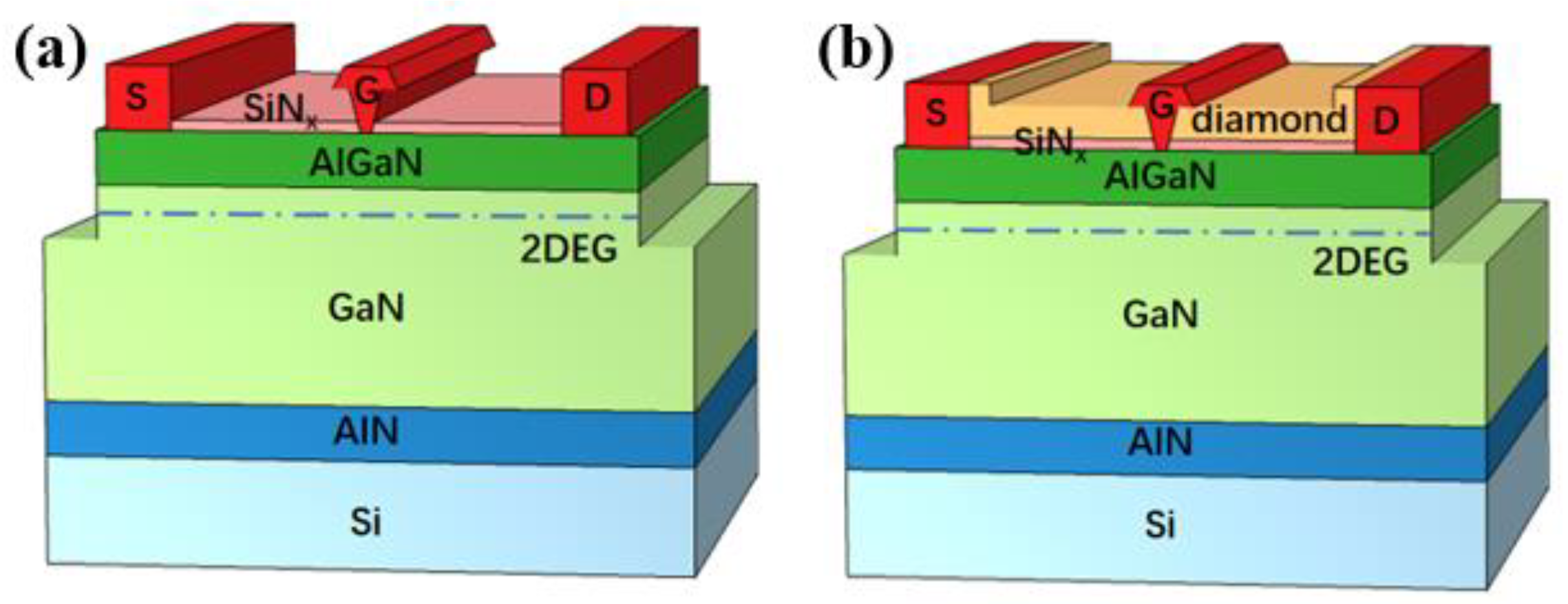
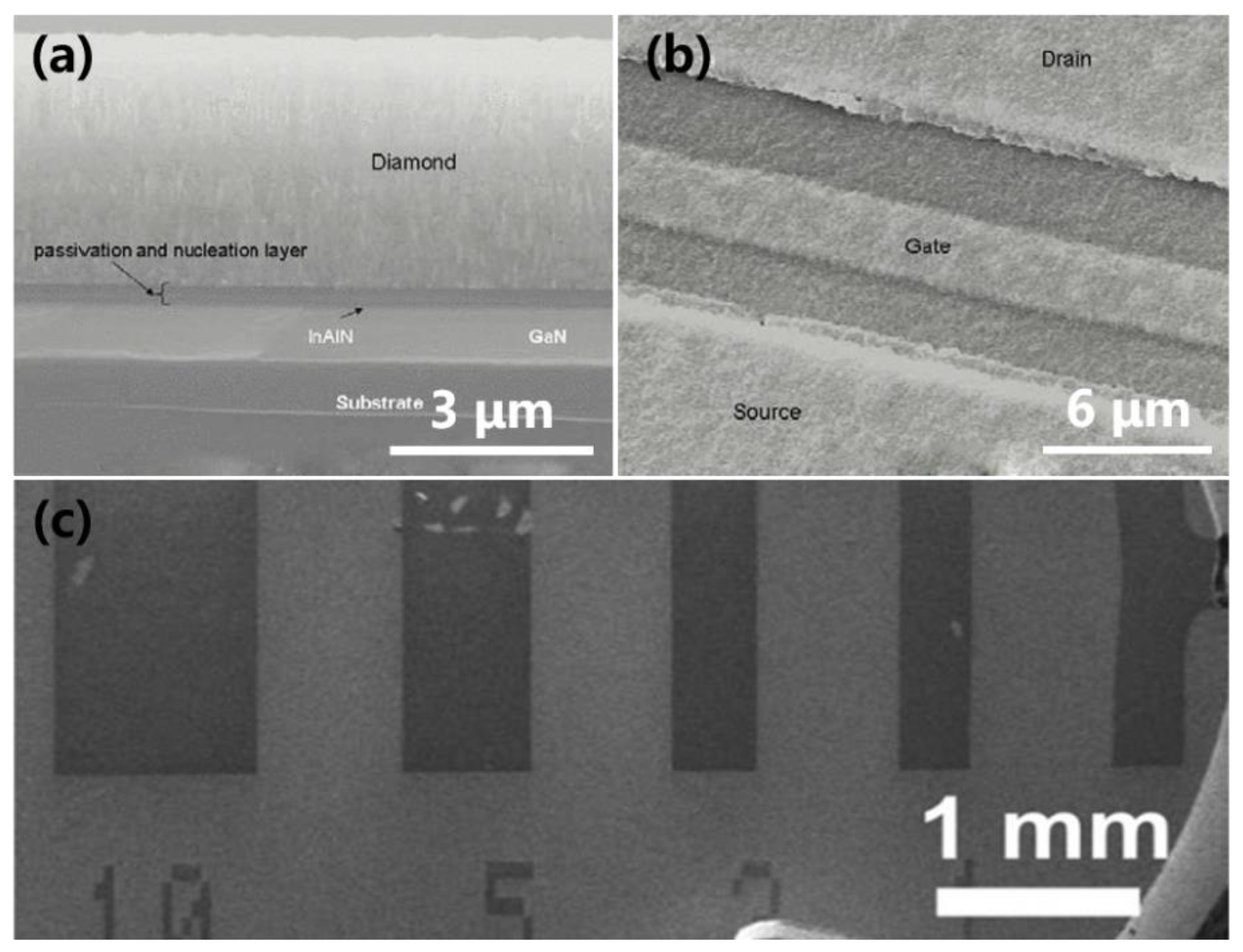
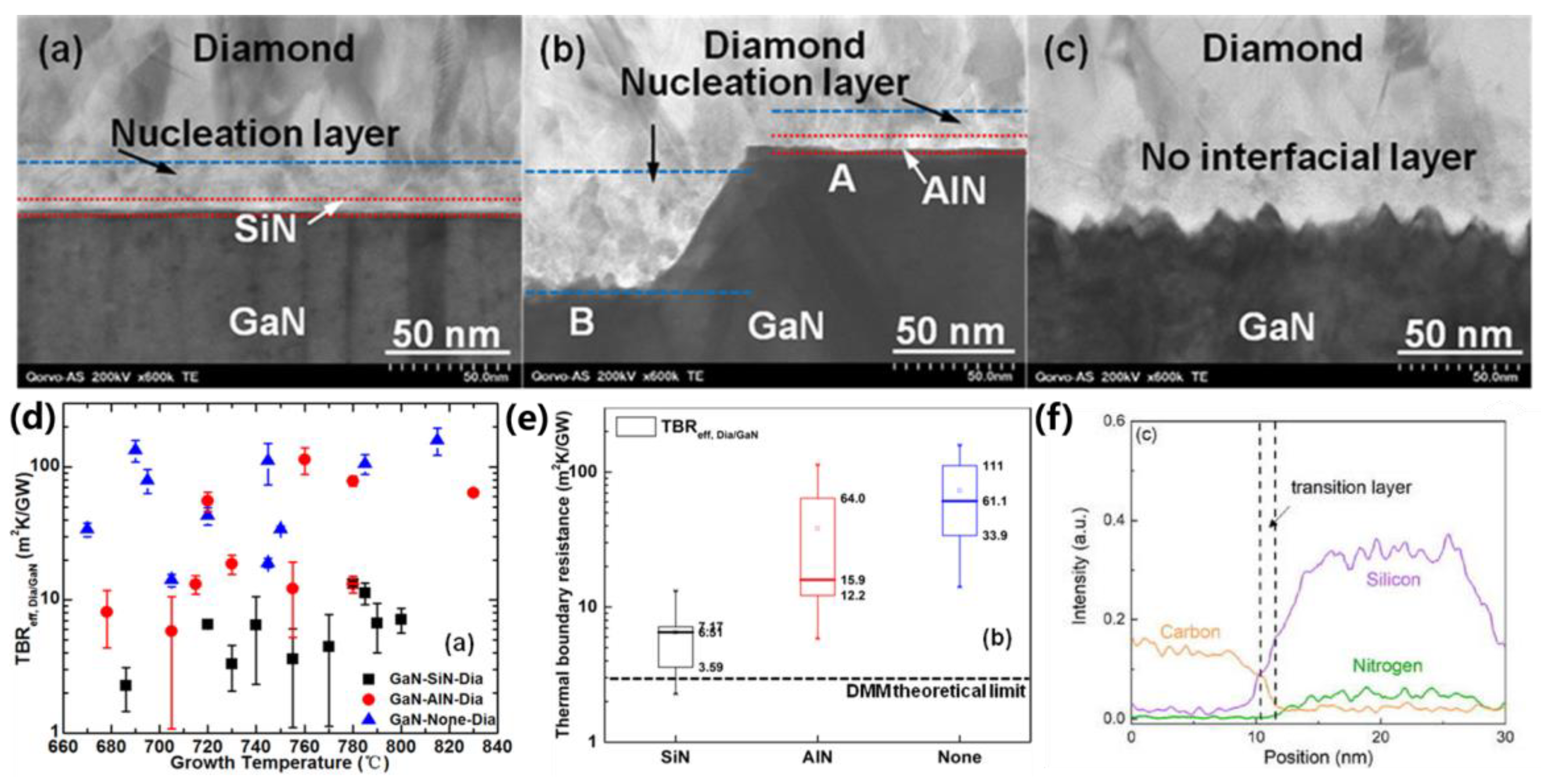
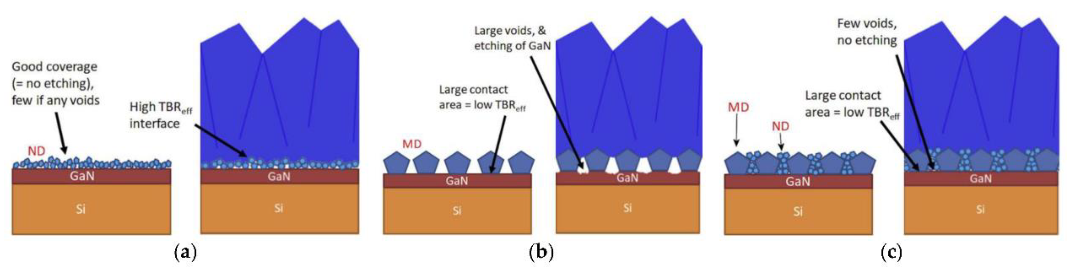
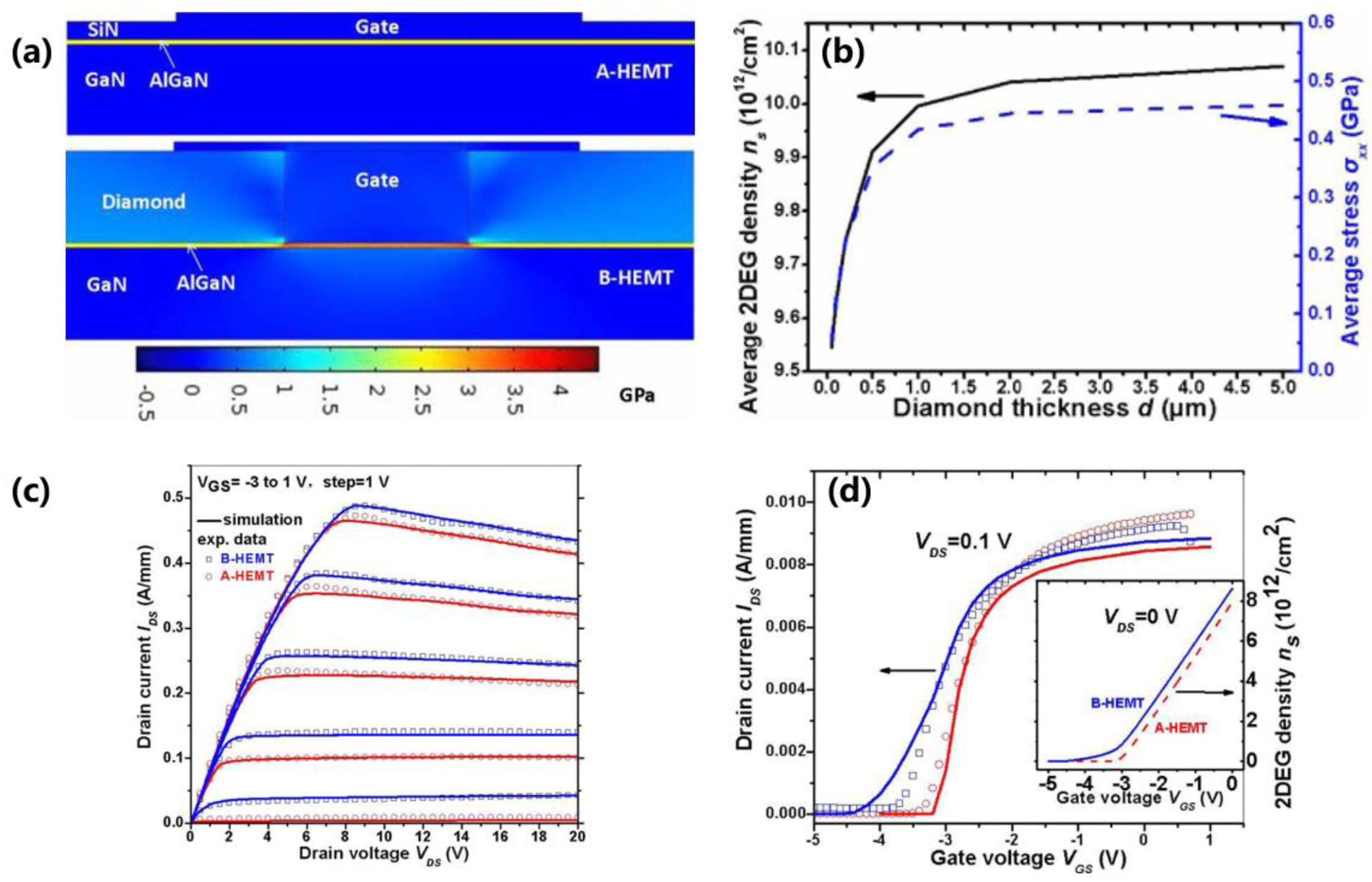
5. Structure and Interface of Diamond on GaN HEMT

A dielectric layer is usually used to protect the GaN and to evenly deposit diamond seeds. Moreover, increasing nitrogen partial pressure and the pre-deposition of a protective layer on the surface of GaN can be also used to raise the GaN stability [101]. However, inherent to the growth of GaN HEMTs, a dielectric layer is placed between the GaN and diamond, which can contribute significantly to the overall thermal resistance of the structure [6]. The requirement for the protective layer is to have plasma insulation, which can effectively prevent the penetration of hydrogen [102], and have good binding properties for both GaN and diamond. The commonly used dielectric layers include SiN, AlN, and SiO2, etc., and the high-quality SiN layer is easily obtained and can form a strong binding transition layer with C atoms. Therefore, SiN film is also considered the primary candidate of dielectric layers. Nowadays, reducing thermal boundary resistance is the important task for the dielectric layer.
First of all, the main measurement methods of thermal boundary resistance are the three-dimensional (3D) Raman thermography mapping method, transient thermoreflectance (TTR), and time-domain thermoreflectance (TDTR). Moreover, the value of thermal boundary resistance can be calculated using the phonon mismatch and diffusion mismatch model (DMM) [103]. At present, the effective thermal boundary resistance (TBReff) is considered to be a thermal parameter that can effectively measure the heat transfer among GaN/interlayer/diamond, which mainly includes the thermal resistance generated by the interface layer, the inherent thermal resistance of the material boundary, and the thermal resistance increased by the crystal defects near the interface, etc. [104].
Cho et al. studied the phonon transient mechanism at the GaN/SiN/diamond interface in detail [105]. They pointed out that the defects of the materials and the phonon scattering caused by the interface determine the thermal resistance at the heterogeneous interface. At the same time, the defects and phonon scattering are closely related to the type and thickness of the dielectric layers and the quality of the diamond-nucleation layer. Therefore, a good abrupt interface layer is a necessary condition for achieving low thermal resistance.
Optimizing the type and thickness of the dielectric layers can effectively reduce the thermal boundary resistance and enhance the thermal-diffusion effect of GaN HEMT devices. Yates et al. used diamond samples with different interface layers (SiN, AlN, and no interfacial layer) to prepare three kinds of GaN-on-diamond samples [50]. According to time-domain thermal-reflectance (TDTR) analysis, the sample with SiN as the interfacial layer has the lowest thermal boundary resistance (<10 m2 K GW−1) with a 5 nm thickness. In contrast, the remaining samples with AlN and no interfacial layer yielded higher TBR values (>20 m2 K GW−1). The corresponding results are shown in Figure 9a–e.
Theoretically, the AlN thermal conductivity is higher than that of the SiN interlayer. Thus, at the same thickness of dielectric layers, the TBR with a diamond/AlN/GaN structure should be lower than that with a SiN interlayer structure. However, during the diamond deposition process, using AlN as the interfacial layer or no interfacial layer of the sample, which will be attributed to the rough interface, this deteriorating interface will enhance the phonon-scattering effect and will not be conducive to heat spreading. This was also verified by Jia et al. and Zhou et al. [50,104,106,108]. The TBR obtained with 100 nm-thick AlN and SiN dielectric layers is 56.4 and 38.5 m2·K/GW, respectively. Thus, SiN is still the better choice. This is because it can better reduce the etching of GaN during the growth process and can result in relatively smooth and orderly elemental transition throughout the interlayer, thereby reducing disorder and enhancing phonon transport across the interface. It is worth noting that the quality of AlN has an important influence on the value of interface thermal resistance. Depositing a high-quality AlN layer is a necessary condition to reduce the interface thermal resistance and give free rein to the high thermal conductivity of AlN itself. The main results of different interlayers are summarized in Table 4.
Use of the periodic patterned SiN layer structure can effectively increase the diamond-nucleation density, reduce the thermal boundary resistance among GaN/SiN/diamond, and improve the heat-dissipation capability of GaN-on-diamond by Jia et al. [114]. This is because the periodic structure increases the contact area of the interface and phonon transmission efficiency, while increasing the nucleation density further reduces the adverse effect on interface heat transfer. Moreover, in the experiment of depositing 1.5 μm-thick polycrystalline diamond on an AlGaN/GaN heterojunction with a 20 nm SiN interlayer, Wu et al. analyzed the interface via transmission electron microscopy (TEM) and electron energy loss spectroscopy (EELS) [107]. The results showed that the thickness of the SiN layer was reduced by ~1.7 nm after diamond growth (Figure 9f), and it was converted into a thin SiC layer at the diamond/SiN interface, which is formed by the possible substitution of N atoms by C atoms. The SiC transition layer can adjust the heat transfer of the diamond/SiN interface, which is conducive to thermal spreading. Therefore, the formation of an Si-C covalent bond might provide a new way to further reduce the thermal resistance of the diamond/GaN interface. This is similarly illustrated in other papers [113,115].
In addition, Downey et al. [116] explored the effect of different thicknesses (5–50 nm) of SiN interlayers on the large-signal output power density and channel temperature reduction and found that the SiN layer with a thickness of 50 nm had the highest output power density and power-added efficiency (PAE) at 4 and 10 GHz. They considered that a reduced trapping effect at the NCD/SiN interface or in the NCD layer itself improved the DC-RF dispersion with a 50 nm-thickness SiN interlayer. From the experimental results and thermal modeling, the extracted channel temperature (TCH) shows no obvious dependence on SiN interlayer thickness. The relevant results are shown in Figure 10.
Furthermore, the defects in the interfacial layer and at the interface between different layers can also result in an increase in thermal boundary resistance. This is precisely because of the high-quality interface between diamond and SiN that does not show any voids or defects. Therefore, the thermal boundary resistance has been significantly reduced. Of course, this is closely related to the quality of the deposited SiN itself. Most of the research in this part is only focused on qualitative analysis. Regarding the method of the diamond passivation layer on GaN HEMT, there is not much discussion on the relationship between defect density and phonon scattering at the specific interface, which is mainly due to the difficulty of nano-scale interface characterization and analysis. Similarly, Cho et al. used the related model to try to analyze the phonon conduction in GaN-diamond composite substrates and obtained a boundary thermal resistance as low as 17 m2 K GW−1 when the point defect density was near 3 × 1018 cm−3 [105]. Meanwhile, optimizing the quality of the diamond-nucleation layer can also provide a positive effect on reducing the thermal boundary resistance. As mentioned above, DND particles can effectively increase the number of diamond nucleation sites. Although DND particles have higher seeding densities, it may not be the best choice for thermal management applications, which is also because of the high TBR value between diamond and substrate. Specifically, a so-called diamond nucleation region exists in the initial diamond seeds, which contains a high concentration of defects and grain boundaries. Thus, this layer increases phonon scattering and consequently reduces thermal conductivity [52]. DND particles with an amorphous shell will lead to an increase in sp2 bonds close to the interface [117]. Secondly, the high seed density means that they are not allowed to grow significantly before coalescing with each other, and this results in a further increase in the number of defects and grain boundaries.
On the other hand, the grain/grain boundaries ratio may be effectively improved by seeding diamond powders with larger particle sizes. In 2020, Bai et al. evaluated the thermal conductivity of deposited diamond films via a 4 and 20 nm diamond particle-seeding process on Si substrates [118]. The seeding densities are 7 × 109 cm−2 with 20 nm seeds and 3 × 1011 cm−2 with 4 nm seeds, respectively. Although the larger-size diamond seeds lead to smaller seeding densities on the substrate surface, they would produce larger-sized grains (indicating larger contact area) near the interface region and have higher thermal conductivity. Smith et al. [109] used the mixed seeds of microdiamond and nanodiamond for pretreatment and deposited CVD diamond on GaN and AlN thin films on Si substrates. They proposed a two-step seeding method using microcrystalline diamond and then continuous seeding with nano-diamond particles, as is shown in Figure 11. The thermal properties were measured via transient thermal reflection (TTR), and an extremely low TBR value of 1.47 m2·K/GW was obtained at the diamond/AlN interface, 30 times smaller than that of films using nanodiamond seeding alone.
Due to the large lattice constant and thermal expansion coefficient difference between GaN and diamond, thermal stress concentration will occur during the deposition of diamond films [119,120], which will lead to the easy shedding of the diamond film and the deterioration of the overall performance of the device. It is very important to perform stress analysis and stress reduction. The thermal stress will accumulate at the GaN/diamond interface via a CTE mismatch. Mismatch will change the stress–strain state in the AlGaN/GaN heterostructures and further have a significant impact on the 2DEG characteristics. The residual stress is related to the thickness of GaN, the deposition temperature of diamond, and the kind of interlayer, as well as other factors [108,121]. Based on the Raman shift of the diamond peak position, Ižák et al. used a temperature-dependent Raman method to measure the thermally induced stress with different temperatures (50–400 °C) and diamond thicknesses (0.78 and 2.8 μm) [122]. As the temperature increases from 50 °C to 400 °C, the stress value decreases from 0.27 GPa to 0.18 GPa. Moreover, with a thickness of diamond layers from 0.78 μm and 2.8 μm, the stress decreases from 0.32 GPa to 0.1 GPa.
Various simulation methods have been used to study the thermal stress and strain generated during diamond deposition on a GaN substrate [121,123,124,125]. Cuenca et al. calculated the expected thermal stress in the circular membranes by establishing a finite element model and investigated the related effects of varying the geometric shape, materials, and temperature. It was found that the membrane deformation during the heating process defines the structure after cooling to room temperature [125]. Therefore, reducing the deformation will significantly improve the overall thermal stress generation. Wang et al. reported the electrical performance of the GaN-based devices based on the internal stress of the diamond capping layer, as shown in Figure 12. Their results show that there is highly localized heat dissipation, high thermal stress, and high inverse piezoelectric stress at the drain side of the gate edge, which leads to obvious mechanical degradation of the devices. Specifically, the stress in the passivation layer will affect the total stress at the gate edge. The compressive stress in the passivation layer will decrease the mechanical degradation of the device, but will cause greater electrical performance damage. When tensile stress occurs, the effect will be the opposite. In addition, the quality of the diamond film itself will have a certain impact on stress generation. The discontinuity of the films will lead to the generation of additional shear stress. Zhang et al. [124] studied the changes in the static and dynamic thermo-mechanical response in AlGaN/GaN HEMTs. Using diamond as the heat spreader, the decrease in peak temperature and the increase in thermal stress need to be weighed. It was found that the peak temperature can be effectively reduced by 45–60 K. Regarding 300 K as a reference, the maximum temperature can occur with a decrease of 30–40%. In addition, a reasonable increase in the diamond layers’ thickness can improve the thermal reliability. The 10 μm diamond layer can reduce the maximum temperature by about 40%. However, mainly due to the large Young ‘s modulus of diamond material and the large thermal expansion coefficient difference between diamond and contact materials, it is worth noting that the max thermal stress value of GaN HEMT will increase by 4–5 times after adding the diamond heat spreader. In 2021, in order to release the points and thermal mismatch caused by localized stress, Jia et al. proposed a double-sided diamond deposition technology to prepare a low-stress GaN-on-diamond structure [126]. The stress problem caused by thermal mismatch at the interface has been better solved. They obtained a tensile stress as low as ~0.5 GPa of the GaN-on-diamond structure, and the crystal quality of GaN did not deteriorate significantly after the wafer transfer process.

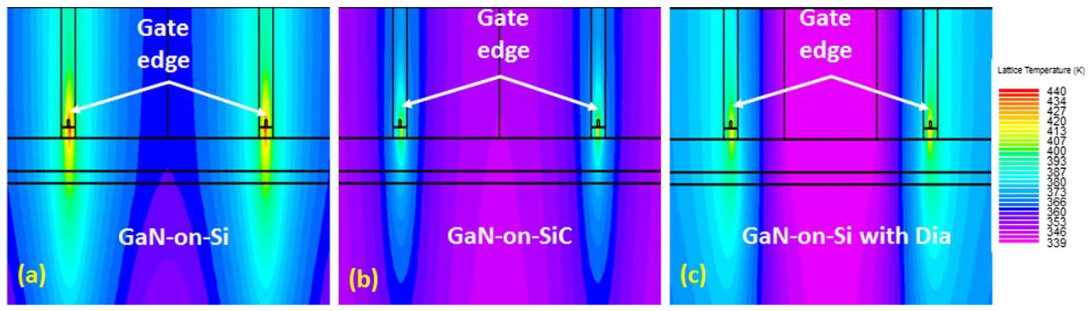
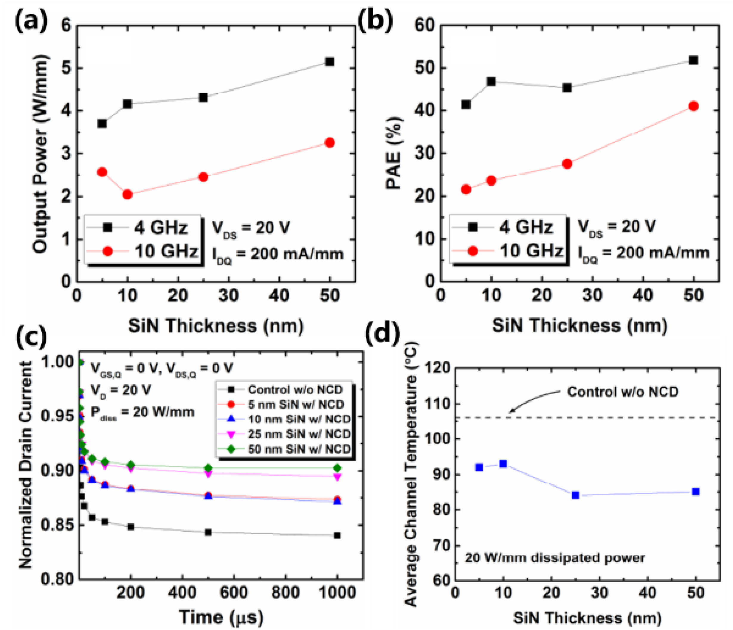
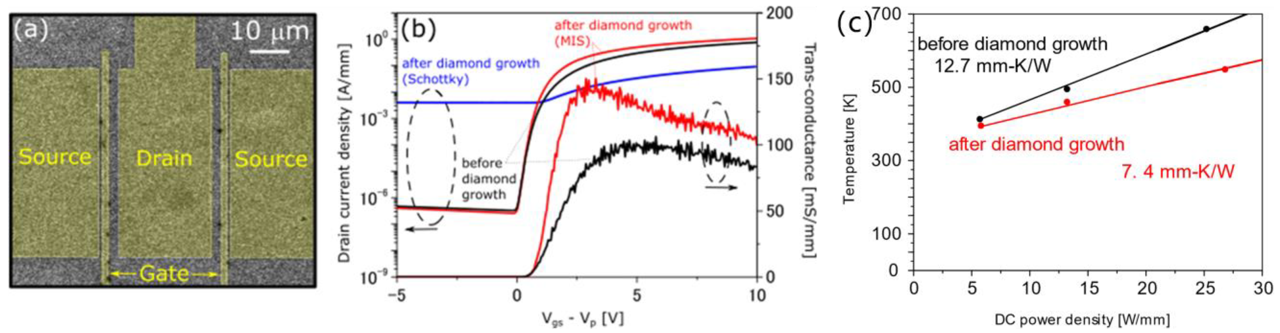
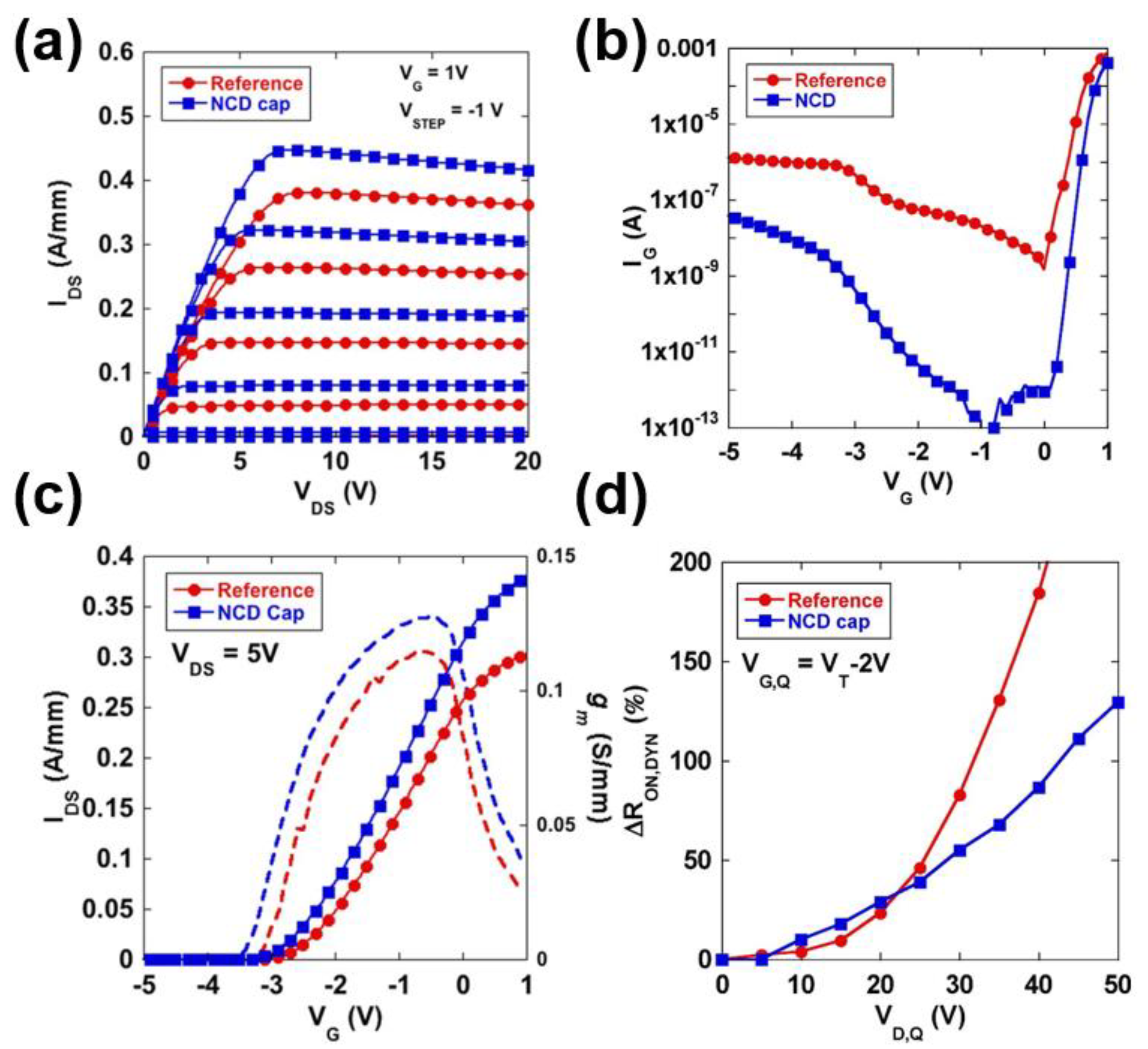
6. Improvement of Device Performance

As above mentioned in Section 2, the performance of the devices may be damaged in the process of growing a diamond layer. How to solve this problem and listing the research progress of device performance improvements are the focus of this section.
Alomari and Dipalo et al. directly grew a nano-diamond film on InAlN/GaN HEMTs and analyzed the electrical properties of the device after diamond growth [65,95,98]. The results showed that InAlN/GaN HEMTs had good compatibility with nano-diamond films, and the current gain cut-off frequency and the maximum oscillation frequency of the device were 4.2 GHz and 5 GHz, respectively. Apart from GaN material, the conventional gate and source and drain electrodes cannot withstand high temperature and hydrogen-rich aggressive conditions. Therefore, some researchers tried to change the kind of electrodes and gate dielectrics. From the research of Gabriel et al. [127], the influence of the diamond-deposition process on Schottky electrode degradation and HEMT electrical characteristics was analyzed. Their group did not use a more conventional Ni/Au metal but compared the stability of the Ir gate electrode and the metal oxide gate electrode layer (IrO2). From their results, IrO2 is an ideal material for preparing stable and high Schottky barrier height (SBH) gate contacts. In 2018, Babchenko’s group [49] complemented the experiment of diamond-coated HEMT devices operating at 500 °C and innovatively proposed the use of high-temperature stable Ir/Al-based gate contacts to prove that AlGaN/GaN-based c-HEMTs coated with diamond/SiNx are functional in the range of room temperature to 500 °C. The U.S. Naval Research Laboratory [128] placed the Boron-doped p+ nanocrystalline diamond (B-NCD) heat-spreading layer in direct contact with the source of self-heating, at the drain side of the gate, replacing the common Ni/Au gate as the gate electrode. Using high-thermal conductivity NCD material, the device channel’s temperature was reduced by 20%. Specially, ID max increased from ≈290 mA/mm to ≈430 mA/mm, the on-resistance decreased from 29.4 to 12.1 Ω·mm, and the leakage gate current decreased by nearly one order of magnitude at a gate voltage of −10 V [129]. In 2014, Meyer and co-workers first introduced an improvement in the large-signal RF output power of GaN HEMTs via NCD top-side coating and focused on the influence of an NCD-capped layer on DC, pulsed, small-signal, and large-signal RF electrical properties [130]. At 4 GHz, the output power density is 5.8 W/mm, the gain is 10.1 dB, and the power added efficiency is 32.6%. Compared with the Schottky gate structure, the 40 nm SiNx MIS gate structure reported by Yaita et al. [131] can remain stable under the condition of high-temperature diamond film deposition. The thermal conductivity of the diamond film reached 200 W m−1 K−1, and the thermal resistance decreased from 12.7 mm K W−1 to 7.4 mm K W−1, as is shown in Figure 13. The Id and gm of the diamond-coated HEMTs increased from 0.9 to 1.1 A/mm and from 102 to 148 mS/mm.
With the development of the technical method, some good experimental results were obtained. The researchers of the Naval Research Laboratory successfully demonstrated a “gate after diamond” approach, which enabled scalable, large-area diamond integration and improved the thermal budget of the process by depositing NCD without degrading the Schottky metal gate [128,132,133,134]. The channel temperature of the NCD-capped device was reduced by 20% up to 10 W/mm of DC power under equivalent power dissipation. This method significantly improved the on-resistance and breakdown voltage, and reduced gate leakage, solving the problem of reduced the on-resistance and breakdown behaviors of the original NCD-capped HEMTs. In the subsequent research, the group optimized the process step again for this mid-process integration scheme [132,133,135]. The NCD layer is allowed to be deposited directly on the GaN surface, which improves the performance of the 2DEG compared to that with the HEMTs passivated with a SiN interlayer. The 2DEG density and mobility are 1.02 × 1013 cm−2 and 1280 cm2/(V·S), which are higher than the original 8.92 × 1012 cm−2 and 1220 cm2/(V·S), respectively. As is shown in Figure 14, ID max and gm peak also increased from 380 to 445 mA/mm and from 114 to 127 mS/mm, while the on-resistance of the device decreased from 14.6 to 11.9 Ω·mm. At the same time, Fujitsu Limited has recently made a breakthrough and has successfully reduced the temperature of GaN HEMT operation by more than 40%. Using the high thermal conductivity of diamond, the temperature can be reduced by 100 °C or more [136]. The improvement in GaN HEMT performance is summarized in Table 5.

7. Conclusions and Outlook

In this study, the approaches of using diamond for effective cooling to eliminate the self-heating effect are systematically summarized. Especially, the method of directly depositing polycrystalline or nanocrystalline diamond at the topside of GaN-based HEMTs, including the nucleation and growth of diamond, structure and interface analysis, and thermal and electronic characterization of GaN HEMTs, is discussed in detail. A nucleation prerequisite for diamond growth on a non-diamond substrate is needed. At present, electrostatic seeding by diamond nanoparticles is the most commonly used seeding method. This method is suitable for most substrates, and the nucleation densities are in excess of 1013 cm−2 using 2 nm DND seeds. Moreover, this is faced with a tough dilemma between growth temperature and device stability in the process of diamond deposition. At present, two-step growth is commonly used: a low-temperature nucleation and high-temperature growth process. The growth temperature of capped diamond on GaN HEMTs is kept at 600–800 °C. At the same time, optimizing the quality and thickness of the interlayer and the nucleation region of diamond are the key points to reduce thermal boundary resistance and stress of the GaN/interlayer/diamond. The extremely low TBR values of 1.47 and 3.1 ± 0.7 m2 K/GW were obtained at the diamond/AlN and diamond/SiN interfaces, respectively.
Apart from the problems of diamond, GaN, and interlayer preparation, in order to avoid damage to the device electrode caused by high temperature deposition, the “gate after growth” method is proposed by the US Naval Laboratory. The leading results are reported that the 2DEG density and mobility are 1.02 × 1013 cm−2 and 1280 cm2/(V·S), which are higher than the original 8.92 × 1012 cm−2 and 1220 cm2/(V·S), respectively. ID max and gm peak also increased from 380 to 445 mA/mm and from 114 to 127 mS/mm, while the on-resistance of the device decreased from 14.6 to 11.9 Ω·mm. Moreover, Fujitsu laboratory has successfully reduced the temperature of GaN HEMT operation by more than 40%.
Although some progress has been made, the main experimental results were obtained by the US Naval Laboratory and Fujitsu Limited. Through all above results, NCD-capped devices have a 20% lower channel temperature at an equivalent power dissipation, and this integration method has great advantages for industry.

Author Contributions

Conceptualization, X.H. (Xiufei Hu), L.G. and X.X. (Xuejian Xie).; collecting and sorting data, Z.L., B.L. and Y.Y.; writing—original draft, Y.W., S.L. and X.W.; writing—review & editing, visualization, M.X., Y.P., X.X. (Xiangang Xu) and X.H. (Xiaobo Hu) All authors have read and agreed to the published version of the manuscript.

Funding

This research received no external funding.

Data Availability Statement

Not applicable.

Conflicts of Interest

The authors declare no conflict of interest.

References

  1. Asif Khan, M.; Bhattarai, A.; Kuznia, J.N.; Olson, D.T. High electron mobility transistor based on a GaN-AlxGa1−xN heterojunction. Appl. Phys. Lett. 1993, 63, 1214–1215. [Google Scholar] [CrossRef]
  2. Wang, X.; Hu, G.; Ma, Z.; Ran, J.; Wang, C.; Xiao, H.; Tang, J.; Li, J.; Wang, J.; Zeng, Y.; et al. AlGaN/AlN/GaN/SiC HEMT structure with high mobility GaN thin layer as channel grown by MOCVD. J. Cryst. Growth 2007, 298, 835–839. [Google Scholar] [CrossRef]
  3. Wang, X.L.; Chen, T.S.; Xiao, H.L.; Tang, J.; Ran, J.X.; Zhang, M.L.; Feng, C.; Hou, Q.F.; Wei, M.; Jiang, L.J.; et al. An internally-matched GaN HEMTs device with 45.2W at 8GHz for X-band application. Solid-State Electron. 2009, 53, 332–335. [Google Scholar] [CrossRef]
  4. Millan, J.; Godignon, P.; Perpina, X.; Perez-Tomas, A.; Rebollo, J. A Survey of Wide Bandgap Power Semiconductor Devices. IEEE Trans. Power Electron. 2014, 29, 2155–2163. [Google Scholar] [CrossRef]
  5. Amano, H.; Baines, Y.; Beam, E.; Borga, M.; Bouchet, T.; Chalker, P.R.; Charles, M.; Chen, K.J.; Chowdhury, N.; Chu, R.; et al. The 2018 GaN power electronics roadmap. J. Phys. D Appl. Phys. 2018, 51, 163001. [Google Scholar] [CrossRef]
  6. Sang, L. Diamond as the heat spreader for the thermal dissipation of GaN-based electronic devices. Funct. Diam. 2021, 1, 174–188. [Google Scholar] [CrossRef]
  7. Sussmann, R.S.; Brandon, J.R.; Scarsbrook, G.A.; Sweeney, C.G.; Valentine, T.J.; Whitehead, A.J.; Wort, C.J.H. Properties of bulk polycrystalline CVD diamond. Diam. Relat. Mater. 1994, 3, 303–312. [Google Scholar] [CrossRef]
  8. Govindaraju, N.; Singh, R.N. Processing of nanocrystalline diamond thin films for thermal management of wide-bandgap semiconductor power electronics. Mater. Sci. Eng. B. 2011, 176, 1058–1072. [Google Scholar] [CrossRef]
  9. Inyushkin, A.V.; Taldenkov, A.N.; Ralchenko, V.G.; Bolshakov, A.P.; Koliadin, A.V.; Katrusha, A.N. Thermal conductivity of high purity synthetic single crystal diamonds. Phys. Rev. B Condens. Matter. 2018, 97, 144305. [Google Scholar] [CrossRef]
  10. Hsu, C.Y.; Lin, Y.L. Junction temperature of high-power LED packages with diamond film. In Proceedings of the 3rd International Nanoelectronics Conference (INEC), Hong Kong, China, 3–8 January 2010. [Google Scholar] [CrossRef]
  11. Chen, P.H.; Lin, C.L.; Liu, Y.K.; Chung, T.Y.; Liu, C.Y. Diamond Heat Spreader Layer for High-Power Thin-GaN Light-Emitting Diodes. IEEE Photonics Technol. Lett. 2008, 20, 845–847. [Google Scholar] [CrossRef]
  12. Francis, D.; Wasserbauer, J.; Faili, F.; Babic, D.; Ejeckam, F.; Hong, W.; Specht, P. GaN-HEMT epilayers on diamond substrates: Recent progress. In Proceedings of the CS MANTECH Conference, Austin, TX, USA, 14–17 May 2007; Available online: https://www.researchgate.net/publication/237386477 (accessed on 7 October 2021).
  13. Shibata, H.; Waseda, Y.; Ohta, H.; Kiyomi, K.; Shimoyama, K.; Fujito, K.; Nagaoka, H.; Kagamitani, Y.; Simura, R.; Fukuda, T. High Thermal Conductivity of Gallium Nitride (GaN) Crystals Grown by HVPE Process. Mater. Trans. 2007, 48, 2782–2786. [Google Scholar] [CrossRef] [Green Version]
  14. Wei, R.; Song, S.; Yang, K.; Cui, Y.; Peng, Y.; Chen, X.; Hu, X.; Xu, X. Thermal conductivity of 4H-SiC single crystals. J. Appl. Phys. 2013, 113, 2782–2786. [Google Scholar] [CrossRef]
  15. Guo, H.; Kong, Y.; Han, P.; Cheng, T. Progress of Chip-level Thermal Management for GaN Power Devices. Res. Prog. SSE 2018, 88, 316–323. [Google Scholar]
  16. Bhatnagar, M.; Baliga, B.J. Comparison of 6H-SiC, 3C-SiC, and Si for power devices. IEEE Trans. Electron Devices 1993, 40, 645–655. [Google Scholar] [CrossRef]
  17. Mishra, U.K.; Parikh, P.; Yi-Feng, W. AlGaN/GaN HEMTs-an overview of device operation and applications. Proc. IEEE 2002, 90, 1022–1031. [Google Scholar] [CrossRef] [Green Version]
  18. Leszczynski, M.; Teisseyre, H.; Suski, T.; Grzegory, I.; Bockowski, M.; Jun, J.; Porowski, S.; Pakula, K.; Baranowski, J.M.; Foxon, C.T.; et al. Lattice parameters of gallium nitride. Appl. Phys. Lett. 1996, 69, 73–75. [Google Scholar] [CrossRef]
  19. Zhu, R.H.; Miao, J.Y.; Liu, J.L.; Chen, L.X.; Guo, J.C.; Hua, C.Y.; Ding, T.; Lian, H.K.; Li, C.M. High temperature thermal conductivity of free-standing diamond films prepared by DC arc plasma jet CVD. Diamond Relat. Mater. 2014, 50, 55–59. [Google Scholar] [CrossRef]
  20. Chao, P.-C.; Chu, K.; Creamer, C.; Diaz, J.; Yurovchak, T.; Shur, M.; Kallaher, R.; McGray, C.; Via, G.D.; Blevins, J.D. Low-Temperature Bonded GaN-on-Diamond HEMTs with 11 W/mm Output Power at 10 GHz. IEEE Trans. Electron Devices 2015, 62, 3658–3664. [Google Scholar] [CrossRef]
  21. Liu, T.; Kong, Y.; Wu, L.; Guo, H.; Zhou, J.; Kong, C.; Chen, T. 3-inch GaN-on-Diamond HEMTs with Device-First Transfer Technology. IEEE Electron Device Lett. 2017, 38, 1417–1420. [Google Scholar] [CrossRef]
  22. Chu, K.K.; Chao, P.C.; Diaz, J.A.; Yurovchak, T.; Creamer, C.T. Low-Temperature Substrate Bonding Technology for High Power GaN-on-Diamond HEMTs. In Proceedings of the Lester Eastman Conference, Ithaca, NY, USA, 5–7 August 2014. [Google Scholar]
  23. Tadjer, M.J.; Anderson, T.J.; Ancona, M.G.; Raad, P.E.; Komarov, P.; Bai, T.; Gallagher, J.C.; Koehler, A.D.; Goorsky, M.S.; Francis, D.A.; et al. GaN-On-Diamond HEMT Technology with TAVG = 176 °C at PDC, max = 56 W/mm Measured by Transient Thermoreflectance Imaging. IEEE Electron Device Lett. 2019, 40, 881–884. [Google Scholar] [CrossRef]
  24. Ejeckam, F.; Francis, D.; Faili, F.; Twitchen, D.; Bolliger, B.; Babic, D.; Felbinger, J. GaN-on-diamond: A brief history. In Proceedings of the 2014 Lester Eastman Conference on High Performance Devices (LEC), Ithaca, NY, USA, 5–7 August 2014. [Google Scholar]
  25. Dussaigne, A.; Gonschorek, M.; Malinverni, M.; Py, M.A.; Martin, D.; Mouti, A.; Stadelmann, P.; Grandjean, N. High-Mobility AlGaN/GaN Two-Dimensional Electron Gas Heterostructure Grown on (111) Single Crystal Diamond Substrate. Jpn. J. Appl. Phys. 2010, 49, 061001. [Google Scholar] [CrossRef]
  26. Alomari, M.; Dussaigne, A.; Martin, D.; Grandjean, N.; Gaquière, C.; Kohn, E. AlGaN/GaN HEMT on (111) single crystalline diamond. Electron. Lett. 2010, 46, 4. [Google Scholar] [CrossRef]
  27. Hirama, K.; Taniyasu, Y.; Kasu, M. AlGaN/GaN high-electron mobility transistors with low thermal resistance grown on single-crystal diamond (111) substrates by metalorganic vapor-phase epitaxy. Appl. Phys. Lett. 2011, 98, 162112. [Google Scholar] [CrossRef]
  28. Hirama, K.; Kasu, M.; Taniyasu, Y. RF High-Power Operation of AlGaN/GaN HEMTs Epitaxially Grown on Diamond. IEEE Electron Device Lett. 2012, 33, 513–515. [Google Scholar] [CrossRef]
  29. Webster, R.F.; Cherns, D.; Kuball, M.; Jiang, Q.; Allsopp, D. Electron microscopy of gallium nitride growth on polycrystalline diamond. Semicond. Sci. Technol. 2015, 30, 114007. [Google Scholar] [CrossRef]
  30. Ahmed, R.; Siddique, A.; Anderson, J.; Gautam, C.; Holtz, M.; Piner, E. Integration of GaN and Diamond Using Epitaxial Lateral Overgrowth. ACS Appl. Mater. Interfaces 2020, 12, 39397–39404. [Google Scholar] [CrossRef]
  31. Tijent, F.Z.; Faqir, M.; Chouiyakh, H.; Essadiqi, E.H. Review—Integration Methods of GaN and Diamond for Thermal Management Optimization. ECS J. Solid State Sci. Technol. 2021, 10, 074003. [Google Scholar] [CrossRef]
  32. William, G.E. Synthesis of Diamond. US Patent 3030188, 17 April 1962. [Google Scholar]
  33. John, C.A.; Herbert, A.W.; Wayne, S.S. Growth of Diamond Seed Crystals by Vapor Deposition. J. Appl. Phys. 1968, 39, 2915. [Google Scholar]
  34. Michael, S.; Knut, P. A review of diamond synthesis by CVD processes. Diam. Relat. Mater. 2011, 20, 1287–1301. [Google Scholar]
  35. Siegal, M.P.; Friedmann, T.A.; Sullivan, J.P.; Mikkalson, J.; Dominguez, F. Diamond and Diamond-Like Carbon Films for Advanced Electronic Applications; Sandia National Lab: Albuquerque, NM, USA.
  36. Arivazhagan, L.; Jarndal, A.; Nirmal, D. GaN HEMT on Si substrate with diamond heat spreader for high power applications. J. Comput. Electron. 2021, 20, 873–882. [Google Scholar] [CrossRef]
  37. Zhang, H.; Guo, Z.; Lu, Y. Enhancement of Hot Spot Cooling by Capped Diamond Layer Deposition for Multifinger AlGaN/GaN HEMTs. IEEE Trans. Electron Devices 2020, 67, 47–52. [Google Scholar] [CrossRef]
  38. Zhang, H.; Guo, Z. Thickness Dependence and Anisotropy of Capped Diamond Thermal Conductivity on Cooling of Pulse-Operated GaN HEMTs. IEEE Trans. Compon. Packag. Manuf. Technol. 2021, 11, 233–240. [Google Scholar] [CrossRef]
  39. Zhang, H.; Guo, Z. Near-junction microfluidic cooling for GaN HEMT with capped diamond heat spreader. Int. J. Heat Mass Transf. 2022, 186, 122476. [Google Scholar] [CrossRef]
  40. Zhou, Y.; Ramaneti, R.; Anaya, J.; Korneychuk, S.; Derluyn, J.; Sun, H.; Pomeroy, J.; Verbeeck, J.; Haenen, K.; Kuball, M. Thermal characterization of polycrystalline diamond thin film heat spreaders grown on GaN HEMTs. Appl. Phys. Lett. 2017, 111, 041901. [Google Scholar] [CrossRef] [Green Version]
  41. Dumka, D.C.; Chou, T.M.; Jimenez, J.L.; Fanning, D.M.; Francis, D.; Faili, F.; Ejeckam, F.; Bernardoni, M.; Pomeroy, J.W.; Kuball, M. Electrical and Thermal Performance of AlGaN/GaN HEMTs on Diamond Substrate for RF Applications. In Proceedings of the 2013 IEEE Compound Semiconductor Integrated Circuit Symposium (CSICS), Monterey, CA, USA, 13–16 October 2013. [Google Scholar]
  42. Blevins, J.D.; Via, G.D.; Sutherlin, K.; Tetlak, S.; Poling, B.; Gilbert, R.; Moore, B.; Hoelscher, J.; Stumpff, B.; Bar-Cohen, A.; et al. Recent Progress in GaN-on-Diamond Device Technology. In Proceedings of the CS MANTECH Conference, Denver, CO, USA, 19–22 May 2014. [Google Scholar]
  43. Via, G.D.; Felbinger, J.G.; Blevins, J.; Chabak, K.; Jessen, G.; Gillespie, J.; Fitch, R.; Crespo, A.; Sutherlin, K.; Poling, B.; et al. Wafer-scale GaN HEMT performance enhancement by diamond substrate integration. Phys. Status Solidi C 2014, 11, 871–874. [Google Scholar] [CrossRef]
  44. Pomeroy, J.; Bernardoni, M.; Sarua, A.; Manoi, A.; Dumka, D.C.; Fanning, D.M.; Kuball, M. Achieving the Best Thermal Performance for GaN-on-Diamond. In Proceedings of the 2013 IEEE Compound Semiconductor Integrated Circuit Symposium (CSICS), Monterey, CA, USA, 13–16 October 2013. [Google Scholar]
  45. Oba, M.; Sugino, T. Growth of (111)-Oriented Diamond Grains on Hexagonal GaN. Jpn. J. Appl. Phys. 2000, 39, L1213. [Google Scholar]
  46. Francis, D.; Faili, F.; Babić, D.; Ejeckam, F.; Nurmikko, A.; Maris, H. Formation and characterization of 4-inch GaN-on-diamond substrates. Diam. Relat. Mater. 2010, 19, 229–233. [Google Scholar] [CrossRef]
  47. Dumka, D.C.; Chou, T.M.; Faili, F.; Francis, D.; Ejeckam, F. AlGaN/GaN HEMTs on diamond substrate with over 7 W/mm output power density at 10 GHz. Electron. Lett. 2013, 49, 1298–1299. [Google Scholar] [CrossRef]
  48. Sun, H.; Pomeroy, J.W.; Simon, R.B.; Francis, D.; Faili, F.; Twitchen, D.J.; Kuball, M. Temperature-Dependent Thermal Resistance of GaN-on-Diamond HEMT Wafers. IEEE Electron Device Lett. 2016, 37, 621–624. [Google Scholar] [CrossRef]
  49. Babchenko, O.; Vanko, G.; Gerboc, M.; Ižák, T.; Vojs, M.; Lalinský, T.; Kromka, A. Study on electronic properties of diamond/SiNx-coated AlGaN/GaN high electron mobility transistors operating up to 500 °C. Diam. Relat. Mater. 2018, 89, 266–272. [Google Scholar] [CrossRef]
  50. Yates, L.; Anderson, J.; Gu, X.; Lee, C.; Bai, T.; Mecklenburg, M.; Aoki, T.; Goorsky, M.S.; Kuball, M.; Piner, E.L.; et al. Low Thermal Boundary Resistance Interfaces for GaN-on-Diamond Devices. ACS Appl. Mater. Interfaces 2018, 10, 24302–24309. [Google Scholar] [CrossRef]
  51. Toshihiro, O.; Atsushi, Y.; Yuichi, M.; Kozo, M.; Junji, K.; Shiro, O.; Masaru, S.; Naoya, O.; Kazukiyo, J.; Norikazu, N. An Over 20-W/mm S-Band InAlGaN/GaN HEMT with SiC/Diamond-Bonded Heat Spreader. IEEE Electron Device Lett. 2019, 40, 287–290. [Google Scholar]
  52. Babchenko, O.; Dzuba, J.; Lalinský, T.; Vojs, M.; Vincze, A.; Ižák, T.; Vanko, G. Stability of AlGaN/GaN heterostructures after hydrogen plasma treatment. Appl. Surf. Sci. 2017, 395, 92–97. [Google Scholar] [CrossRef]
  53. Mendes, J.C.; Liehr, M.; Li, C. Diamond/GaN HEMTs: Where from and Where to? Materials 2022, 15, 415. [Google Scholar] [CrossRef]
  54. Yeh, Y.-H.; Chen, K.-M.; Wu, Y.-H.; Hsu, Y.-C.; Yu, T.-Y.; Lee, W.-I. Hydrogen etching of GaN and its application to produce free-standing GaN thick films. J. Cryst. Growth 2011, 333, 16–19. [Google Scholar] [CrossRef]
  55. Koukitu, A.; Mayumi, M.; Kumagai, Y. Surface polarity dependence of decomposition and growth of GaN studied using in situ gravimetric monitoring. J. Cryst. Growth 2002, 246, 230–236. [Google Scholar] [CrossRef]
  56. Mandal, S. Nucleation of diamond films on heterogeneous substrates: A review. RSC Adv. 2021, 11, 10159–10182. [Google Scholar] [CrossRef] [PubMed]
  57. Cardoso, J.; Harsdorff, M. The Influence of Surface Defects on the Heterogeneous Nucleation and Growth of Thin Films. Z. Nat. A 2014, 33, 442–446. [Google Scholar] [CrossRef]
  58. Kromka, A.; Babchenko, O.; Potocky, S.; Rezek, B.; Sveshnikov, A.; Demo, P.; Izak, T.; Varga, M. Diamond nucleation and seeding techniques for tissue regeneration. Diam. -Based Mater. Biomed. Appl. 2013, 206–255. [Google Scholar]
  59. Spitsyn, B.V.; Bouilov, L.L.; Derjaguin, B.V. Vapor growth of diamond on diamond and other surfaces. J. Cryst. Growth 1981, 52, 219–226. [Google Scholar] [CrossRef]
  60. Schweitz, K.O.; Schou-Jensen, R.B.; Eskildsen, S.S. Ultrasonic pre-treatment for enhanced diamond nucleation. Diam. Relat. Mater. 1996, 5, 206–210. [Google Scholar] [CrossRef]
  61. Mohapatra, D.R.; Rai, P.; Misra, A.; Tyagi, P.K.; Yadav, B.S.; Misra, D.S. Parameter window of diamond growth on GaN films by microwave plasma chemical vapor deposition. Diam. Relat. Mater. 2008, 17, 1775–1779. [Google Scholar] [CrossRef]
  62. Yugo, S.; Kanai, T.; Kimura, T.; Muto, T. Generation of diamond nuclei by electric field in plasma chemical vapor deposition. Appl. Phys. Lett. 1991, 58, 1036–1038. [Google Scholar] [CrossRef]
  63. Lifshitz, Y.; Köhler, T.; Frauenheim, T.; Guzmann, I.; Hoffman, A.; Zhang, R.Q.; Zhou, X.T.; Lee, S.T. The Mechanism of Diamond Nucleation from Energetic Species. Science 2002, 297, 1531–1533. [Google Scholar] [CrossRef]
  64. Oba, M.; Sugino, T. Oriented growth of diamond on (0001) surface of hexagonal GaN. Diam. Relat. Mater. 2001, 10, 1343–1346. [Google Scholar] [CrossRef]
  65. Alomari, M.; Dipalo, M.; Rossi, S.; Diforte-Poisson, M.A.; Delage, S.; Carlin, J.F.; Grandjean, N.; Gaquiere, C.; Toth, L.; Pecz, B.; et al. Diamond overgrown InAlN/GaN HEMT. Diam. Relat. Mater. 2011, 20, 604–608. [Google Scholar] [CrossRef]
  66. Kohn, E.; Alomari, M.; Gao, Z.; Rossi, S.; Dussaigne, A.; Carlin, J.-F.; Grandjean, N.; Aretouli, K.E.; Adikimenakis, A.; Konstantinidis, G.; et al. Direct Interpretation of Diamond Heat Spreader with GaN-Based HEMT Device Structures. In Proceedings of the High Performance Devices. Lester Eastman Conference (LEC), Ithaca, NY, USA, 5–7 August 2014; pp. 1–4. [Google Scholar]
  67. Williams, O.A.; Douhéret, O.; Daenen, M.; Haenen, K.; Ōsawa, E.; Takahashi, M. Enhanced diamond nucleation on monodispersed nanocrystalline diamond. Chem. Phys. Lett. 2007, 445, 255–258. [Google Scholar] [CrossRef]
  68. Girard, H.A.; Perruchas, S.; Gesset, C.; Chaigneau, M.; Vieille, L.; Arnault, J.C.; Bergonzo, P.; Boilot, J.P.; Gacoin, T. Electrostatic grafting of diamond nanoparticles: A versatile route to nanocrystalline diamond thin films. ACS Appl. Mater. Interfaces 2009, 1, 2738–2746. [Google Scholar] [CrossRef] [PubMed]
  69. Hees, J.; Kriele, A.; Williams, O.A. Electrostatic self-assembly of diamond nanoparticles. Chem. Phys. Lett. 2011, 509, 12–15. [Google Scholar] [CrossRef]
  70. Wiese, G.R.; Healy, T.W. Effect of particle size on colloid stability. R. Soc. Chem. 1970, 66, 490–499. [Google Scholar] [CrossRef]
  71. Williams, O.A.; Hees, J.; Dieker, C.; Jäger, W.; Kirste, L.; Nebel, C.E. Size-Dependent Reactivity of Diamond Nanoparticles. ACS Nano 2010, 4, 4824–4830. [Google Scholar] [CrossRef]
  72. Gines, L.; Mandal, S.; Morgan, D.J.; Lewis, R.; Davies, P.R.; Borri, P.; Morley, G.W.; Williams, O.A. Production of Metal-Free Diamond Nanoparticles. ACS Omega 2018, 3, 16099–16104. [Google Scholar] [CrossRef]
  73. Ozawa, M.; Inaguma, M.; Takahashi, M.; Kataoka, F.; Krüger, A.; Ōsawa, E. Preparation and Behavior of Brownish, Clear Nanodiamond Colloids. Adv. Mater. 2007, 19, 1201–1206. [Google Scholar] [CrossRef]
  74. Stehlik, S.; Varga, M.; Stenclova, P.; Ondic, L.; Ledinsky, M.; Pangrac, J.; Vanek, O.; Lipov, J.; Kromka, A.; Rezek, B. Ultrathin Nanocrystalline Diamond Films with Silicon Vacancy Color Centers via Seeding by 2 nm Detonation Nanodiamonds. ACS Appl. Mater. Interfaces 2017, 9, 38842–38853. [Google Scholar] [CrossRef] [PubMed]
  75. Mandal, S.; Thomas, E.L.H.; Middleton, C.; Gines, L.; Griffiths, J.T.; Kappers, M.J.; Oliver, R.A.; Wallis, D.J.; Goff, L.E.; Lynch, S.A.; et al. Surface Zeta Potential and Diamond Seeding on Gallium Nitride Films. ACS Omega 2017, 2, 7275–7280. [Google Scholar] [CrossRef]
  76. Girard, H.A.; Scorsone, E.; Saada, S.; Gesset, C.; Arnault, J.C.; Perruchas, S.; Rousseau, L.; David, S.; Pichot, V.; Spitzer, D.; et al. Electrostatic grafting of diamond nanoparticles towards 3D diamond nanostructures. Diam. Relat. Mater. 2012, 23, 83–87. [Google Scholar] [CrossRef]
  77. Santos, M.; Campos, R.A.; Azevedo, A.F.; Baldan, M.R.; Ferreira, N.G. Nanocrystalline Diamond Films Prepared with Different Diamond Seeding Processes of 4 Nm and 0.25 Μm Diamond Powders. Mater. Sci. Forum 2014, 802, 146–151. [Google Scholar] [CrossRef]
  78. Domonkos, M.; Ižák, T.; Kromka, A.; Varga, M. Polymer-based nucleation for chemical vapour deposition of diamond. J. Appl. Polym. Sci. 2016, 133, 43688. [Google Scholar] [CrossRef]
  79. Scorsone, E.; Saada, S.; Arnault, J.C.; Bergonzo, P. Enhanced control of diamond nanoparticle seeding using a polymer matrix. J. Appl. Phys. 2009, 106, 014908. [Google Scholar] [CrossRef]
  80. Izak, T.; Babchenko, O.; Jirásek, V.; Vanko, G.; Vallo, M.; Vojs, M.; Kromka, A. Selective area deposition of diamond films on AlGaN/GaN heterostructures. Phys. Status Solidi B 2014, 251, 2574–2580. [Google Scholar] [CrossRef]
  81. Das, D.; Singh, R.N. A review of nucleation, growth and low temperature synthesis of diamond thin films. Int. Mater. Rev. 2007, 52, 29–64. [Google Scholar] [CrossRef]
  82. Zhang, W.; Xia, Y.; Shi, W.; Wang, L.; Fang, Z. Effect of substrate temperature on the selective deposition of diamond films. Diam. Relat. Mater. 2000, 9, 1687–1690. [Google Scholar] [CrossRef]
  83. Larijani, M.M.; Navinrooz, A.; Le Normand, F. The bias-assisted HF CVD nucleation of diamond: Investigations on the substrate temperature and the filaments location. Thin Solid Film 2006, 501, 206–210. [Google Scholar] [CrossRef]
  84. Silva, W.M.; Ferreira, N.G.; Travello, J.; Almeida, E.C.; Azevedo, A.F.; Baldan, M.R. Dependence of diamond nucleation and growth through graphite etching at different temperatures. Diam. Relat. Mater. 2007, 16, 1705–1710. [Google Scholar] [CrossRef]
  85. Frenklach, M. The role of hydrogen in vapor deposition of diamond. J. Appl. Phys. 1989, 65, 5142–5149. [Google Scholar] [CrossRef]
  86. Goodwin, D.G. Scaling laws for diamond chemical-vapor deposition. I. Diamond surface chemistry. J. Appl. Phys. 1993, 74, 6888–6894. [Google Scholar] [CrossRef] [Green Version]
  87. Butler, J.E.; Woodin, R.L. Thin film diamond growth mechanisms. Philos. Trans. R. Soc. A 1993, 342, 209–224. [Google Scholar]
  88. Harris, S.J.; Weiner, A.M. Reaction kinetics on diamond: Measurement of H atom destruction rates. J. Appl. Phys. 1993, 74, 1022–1026. [Google Scholar] [CrossRef]
  89. Dawnkaski, E.J.; Srivastava, D.; Garrison, B.J. Time dependent Monte Carlo simulations of H reactions on the diamond {001}(2×1) surface under chemical vapor deposition conditions. J. Chem. Phys. 1995, 102, 9401–9411. [Google Scholar] [CrossRef] [Green Version]
  90. Butler, J.E.; Mankelevich, Y.A.; Cheesman, A.; Ma, J.; Ashfold, M.N. Understanding the chemical vapor deposition of diamond: Recent progress. J Phys. Condens. Matter. 2009, 21, 364201. [Google Scholar] [CrossRef] [PubMed]
  91. Butler, J.E.; Sumant, A.V. The CVD of Nanodiamond Materials. Chem. Vap. Depos. 2008, 14, 145–160. [Google Scholar] [CrossRef]
  92. Williams, O.A.; Nesladek, M.; Daenen, M.; Michaelson, S.; Hoffman, A.; Osawa, E.; Haenen, K.; Jackman, R.B. Growth, electronic properties and applications of nanodiamond. Diam. Relat. Mater. 2008, 17, 1080–1088. [Google Scholar] [CrossRef]
  93. Malakoutian, M.; Ren, C.; Woo, K.; Li, H.; Chowdhury, S. Development of Polycrystalline Diamond Compatible with the Latest N-Polar GaN mm-Wave Technology. Cryst. Growth Des. 2021, 21, 2624–2632. [Google Scholar] [CrossRef]
  94. Seelmann-Eggebert, M.; Meisen, P.; Schaudel, F.; Koidl, P.; Vescan, A.; Leier, H. Heat-spreading diamond films for GaN-based high-power transistor devices. Diam. Relat. Mater. 2001, 10, 744–749. [Google Scholar] [CrossRef]
  95. Dipalo, M.; Alomari, M.; Carlin, J.F.; Grandjean, N.; Diforte-Poisson, M.A.; Delage, S.L.; Kohn, E. Thick nano-crystalline diamond overgrowth on InAlN/GaN devices for thermal management. In Proceedings of the 2009 Device Research Conference, University Park, PA, USA, 22–24 June 2009. [Google Scholar]
  96. Goyal, V.; Sumant, A.V.; Teweldebrhan, D.; Balandin, A.A. Direct Low-Temperature Integration of Nanocrystalline Diamond with GaN Substrates for Improved Thermal Management of High-Power Electronics. Adv. Funct. Mater. 2012, 22, 1525–1530. [Google Scholar] [CrossRef]
  97. Tadjer, M.J.; Anderson, T.J.; Hobart, K.D.; Feygelson, T.I.; Caldwell, J.D.; Eddy, C.R.; Kub, F.J.; Butler, J.E.; Pate, B.; Melngailis, J. Reduced Self-Heating in AlGaN/GaN HEMTs Using Nanocrystalline Diamond Heat-Spreading Films. IEEE Electron Device Lett. 2012, 33, 23–25. [Google Scholar] [CrossRef]
  98. Malakoutian, M.; Laurent, M.A.; Chowdhury, S. A Study on the Growth Window of Polycrystalline Diamond on Si3N4-coated N-Polar GaN. Crystals 2019, 9, 498. [Google Scholar] [CrossRef] [Green Version]
  99. Zou, Y.S.; Yang, Y.; Chong, Y.M.; Ye, Q.; He, B.; Yao, Z.Q.; Zhang, W.J.; Lee, S.T.; Cai, Y.; Chu, H.S. Chemical Vapor Deposition of Diamond Films on Patterned GaN Substrates via a Thin Silicon Nitride Protective Layer. Cryst. Growth Des. 2008, 8, 1770–1773. [Google Scholar] [CrossRef]
  100. Babchenko, O.; Izak, T.; Ukraintsev, E.; Hruska, K.; Rezek, B.; Kromka, A. Toward surface-friendly treatment of seeding layer and selected-area diamond growth. Phys. Status Solidi B 2010, 247, 3026–3029. [Google Scholar] [CrossRef]
  101. Han-mei, T.; Jin-long, L.; Liang-xian, C.; Jun-jun, W.; Li-fu, H.; Cheng-ming, L. Decomposition of GaN and Direct Deposition of Nano-diamond Film in Microwave Plasma. J. Synth. Cryst. 2015, 44, 7–12. [Google Scholar]
  102. Izak, T.; Babchenko, O.; Jirásek, V.; Vanko, G.; Vojs, M.; Kromka, A. Influence of Diamond CVD Growth Conditions and Interlayer Material on Diamond/GaN Interface. Mater. Sci. Forum 2015, 821–823, 982–985. [Google Scholar] [CrossRef]
  103. Cho, J.; Li, Z.; Asheghi, M.; Goodson, K.E. Near-junction thermal management: Thermal conduction in gallium nitride composite substrates. Annu. Rev. Heat Transf. 2015, 11, 7–45. [Google Scholar] [CrossRef] [Green Version]
  104. Jia, X.; Wei, J.; Kong, Y.; Li, C.; Liu, J.; Chen, L.; Sun, F.; Wang, X. The influence of dielectric layer on the thermal boundary resistance of GaN-on-diamond substrate. Surf. Interface Anal. 2019, 51, 783–790. [Google Scholar] [CrossRef]
  105. Cho, J.; Francis, D.; Altman, D.H.; Asheghi, M.; Goodson, K.E. Phonon conduction in GaN-diamond composite substrates. J. Appl. Phys. 2017, 121, 055105. [Google Scholar] [CrossRef]
  106. Zhou, Y.; Anaya, J.; Pomeroy, J.; Sun, H.; Gu, X.; Xie, A.; Beam, E.; Becker, M.; Grotjohn, T.A.; Lee, C.; et al. Barrier-Layer Optimization for Enhanced GaN-on-Diamond Device Cooling. ACS Appl. Mater. Interfaces 2017, 9, 34416–34422. [Google Scholar] [CrossRef]
  107. Wu, M.; Cheng, K.; Yang, L.; Hou, B.; Zhang, X.-C.; Wang, P.; Zhang, M.; Zhu, Q.; Zheng, X.-F.; Hu, Y.-S.; et al. Structural and thermal analysis of polycrystalline diamond thin film grown on GaN-on-SiC with an interlayer of 20 nm PECVD-SiN. Appl. Phys. Lett. 2022, 120, 121603. [Google Scholar] [CrossRef]
  108. Siddique, A.; Ahmed, R.; Anderson, J.; Nazari, M.; Yates, L.; Graham, S.; Holtz, M.; Piner, E.L. Structure and Interface Analysis of Diamond on an AlGaN/GaN HEMT Utilizing an in Situ SiNx Interlayer Grown by MOCVD. ACS Appl. Electron. Mater. 2019, 1, 1387–1399. [Google Scholar] [CrossRef]
  109. Smith, E.J.W.; Piracha, A.H.; Field, D.; Pomeroy, J.W.; Mackenzie, G.R.; Abdallah, Z.; Massabuau, F.C.P.; Hinz, A.M.; Wallis, D.J.; Oliver, R.A.; et al. Mixed-size diamond seeding for low-thermal-barrier growth of CVD diamond onto GaN and AlN. Carbon 2020, 167, 620–626. [Google Scholar] [CrossRef]
  110. Cho, J.; Won, Y.; Francis, D.; Asheghi, M.; Goodson, K.E. Thermal Interface Resistance Measurements for GaN-on-Diamond Composite Substrates. In Proceeding of the 2014 IEEE Compound Semiconductor Integrated Circuit Symposium (CSICS), La Jolla, CA, USA, 19–22 October 2014. [Google Scholar]
  111. Sun, H.; Simon, R.B.; Pomeroy, J.W.; Francis, D.; Faili, F.; Twitchen, D.J.; Kuball, M. Reducing GaN-on-diamond interfacial thermal resistance for high power transistor applications. Appl. Phys. Lett. 2015, 106, 111906. [Google Scholar] [CrossRef] [Green Version]
  112. Malakoutian, M.; Field, D.E.; Hines, N.J.; Pasayat, S.; Graham, S.; Kuball, M.; Chowdhury, S. Record-Low Thermal Boundary Resistance between Diamond and GaN-on-SiC for Enabling Radiofrequency Device Cooling. ACS Appl. Mater. Interfaces 2021, 13, 60553–60560. [Google Scholar] [CrossRef]
  113. Field, D.E.; Cuenca, J.A.; Smith, M.; Fairclough, S.M.; Massabuau, F.C.; Pomeroy, J.W.; Williams, O.; Oliver, R.A.; Thayne, I.; Kuball, M. Crystalline Interlayers for Reducing the Effective Thermal Boundary Resistance in GaN-on-Diamond. ACS Appl. Mater. Interfaces 2020, 12, 54138–54145. [Google Scholar] [CrossRef] [PubMed]
  114. Jia, X.; Huang, L.; Sun, M.; Zhao, X.; Wei, J.; Li, C. The Effect of Interlayer Microstructure on the Thermal Boundary Resistance of GaN-on-Diamond Substrate. Coatings 2022, 12, 672. [Google Scholar] [CrossRef]
  115. Liu, J.-L.; Tian, H.-M.; Chen, L.-X.; Wei, J.-J.; Hei, L.-F.; Li, C.-M. Prepration of nano-diamond films on GaN with a Si buffer layer. New Carbon Mater. 2016, 31, 518–524. [Google Scholar] [CrossRef]
  116. Downey, B.P.; Meyer, D.J.; Ancona, M.G.; Feygelson, T.I.; Pate, B.B.; Roussos, J.A.; Tadjer, M.J.; Anderson, T.J.; Hardy, M.T.; Nepal, N.; et al. RF Power Performance of Nanocrystalline Diamond Coated InAlN/AlN/GaN HEMTs. ECS Trans. 2016, 75, 85. [Google Scholar] [CrossRef]
  117. Ōsawa, E. Monodisperse single nanodiamond particulates. Pure Appl. Chem. 2008, 80, 1365–1379. [Google Scholar] [CrossRef]
  118. Bai, T.; Wang, Y.; Feygelson, T.I.; Tadjer, M.J.; Hobart, K.D.; Hines, N.J.; Yates, L.; Graham, S.; Anaya, J.; Kuball, M.; et al. Diamond Seed Size and the Impact on Chemical Vapor Deposition Diamond Thin Film Properties. ECS J. Solid State Sci. Technol. 2020, 9, 053002. [Google Scholar] [CrossRef]
  119. Moelle, C.; Klose, S.; Szücs, F.; Fecht, H.J.; Johnston, C.; Chalker, P.R.; Werner, M. Measurement and calculation of the thermal expansion coefficient of diamond. Diam. Relat. Mater. 1997, 6, 839–842. [Google Scholar] [CrossRef]
  120. Reeber, R.R.; Wang, K. Lattice parameters and thermal expansion of GaN. J. Mater. Res. 2011, 15, 40–44. [Google Scholar] [CrossRef]
  121. Hancock, B.L.; Nazari, M.; Anderson, J.; Piner, E.; Faili, F.; Oh, S.; Twitchen, D.; Graham, S.; Holtz, M. Ultraviolet micro-Raman spectroscopy stress mapping of a 75-mm GaN-on-diamond wafer. Appl. Phys. Lett. 2016, 108, 211901. [Google Scholar] [CrossRef] [Green Version]
  122. Ižák, T.; Jirásek, V.; Vanko, G.; Dzuba, J.; Kromka, A. Temperature-dependent stress in diamond-coated AlGaN/GaN heterostructures. Mater. Des. 2016, 106, 305–312. [Google Scholar] [CrossRef]
  123. Wang, A.; Tadjer, M.J.; Anderson, T.J.; Baranyai, R.; Pomeroy, J.W.; Feygelson, T.I.; Hobart, K.D.; Pate, B.B.; Calle, F.; Kuball, M. Impact of Intrinsic Stress in Diamond Capping Layers on the Electrical Behavior of AlGaN/GaN HEMTs. IEEE Trans. Electron Devices 2013, 60, 3149–3156. [Google Scholar] [CrossRef]
  124. Zhang, R.; Zhao, W.S.; Yin, W.Y.; Zhao, Z.G.; Zhou, H.J. Impacts of diamond heat spreader on the thermo-mechanical characteristics of high-power AlGaN/GaN HEMTs. Diam. Relat. Mater. 2015, 52, 25–31. [Google Scholar] [CrossRef]
  125. Cuenca, J.A.; Smith, M.D.; Field, D.E.; Massabuau, F.C.-P.; Mandal, S.; Pomeroy, J.; Wallis, D.J.; Oliver, R.A.; Thayne, I.; Kuball, M.; et al. Thermal stress modelling of diamond on GaN/III-Nitride membranes. Carbon 2021, 174, 647–661. [Google Scholar] [CrossRef]
  126. Jia, X.; Wei, J.; Huang, Y.; Shao, S.; An, K.; Kong, Y.; Liu, J.; Chen, L.; Li, C. Fabrication of low stress GaN-on-diamond structure via dual-sided diamond film deposition. J. Mater. Sci. 2021, 56, 6903–6911. [Google Scholar] [CrossRef]
  127. Gabriel, V.; Tibor, I.; Oleg, B.; Alexander, K. Diamond Coated AlGaN/GaN High Electron Mobility Transiitors—Effect of Deposition Process on Gate Electrode. In Proceedings of the Nano Conference, Brno, Czech Republic, 14–16 October 2015. [Google Scholar]
  128. Koehler, A.D.; Anderson, T.J.; Hobart, K.D.; Tadjer, M.J.; Feygelson, T.I.; Hite, J.K.; Pate, B.B.; Kub, F.J.; Charles, R.; Eddy, J. Boron-Doped P+ Nanocrystalline Diamond Gate Electrode for AlGaN/GaN HEMTs. In Proceedings of the CS MANTECH Conference, Denver, CO, USA, 19–22 May 2014. [Google Scholar]
  129. Anderson, T.J.; Koehler, A.D.; Hobart, K.D.; Tadjer, M.J.; Feygelson, T.I.; Hite, J.K.; Pate, B.B.; Kub, F.J.; Eddy, C.R. Nanocrystalline Diamond-Gated AlGaN/GaN HEMT. IEEE Electron Device Lett. 2013, 34, 1382–1384. [Google Scholar] [CrossRef]
  130. Meyer, D.J.; Koehler, A.D.; Hobart, K.D.; Eddy, C.R.; Feygelson, T.I.; Anderson, T.J.; Roussos, J.A.; Tadjer, M.J.; Downey, B.P.; Katzer, D.S.; et al. Large-Signal RF Performance of Nanocrystalline Diamond Coated AlGaN/GaN High Electron Mobility Transistors. IEEE Electron Device Lett. 2014, 35, 1013–1015. [Google Scholar] [CrossRef]
  131. Yaita, J.; Yamada, A.; Kotani, J. Growth of microcrystalline diamond films after fabrication of GaN high-electron-mobility transistors for effective heat dissipation. Jpn. J. Appl. Phys. 2021, 60, 076502. [Google Scholar] [CrossRef]
  132. Anderson, T.J.; Hobart, K.D.; Tadjer, M.J.; Koehler, A.D.; Imhoff, E.A.; Hite, J.K.; Feygelson, T.I.; Pate, B.B.; Eddy, C.R.; Kub, F.J. Nanocrystalline Diamond Integration with III-Nitride HEMTs. ECS J. Solid State Sci. Technol. 2016, 6, Q3036–Q3039. [Google Scholar] [CrossRef]
  133. Koehler, A.D.; Anderson, T.J.; Tadjer, M.J.; Feygelson, T.I.; Hite, J.K.; Hobart, K.D.; Pate, B.B.; Kub, F.J.; Eddy, C.R., Jr. Topside Nanocrystalline Diamond Integration on AlGaN/GaN HEMTs for High Temperature Operation. Addit. Conf. 2014, 2014, 1–6. [Google Scholar] [CrossRef]
  134. Anderson, T.J.; Hobart, K.D.; Tadjer, M.J.; Koehler, A.D.; Feygelson, T.I.; Pate, B.B.; Hite, J.K.; Kub, F.J.; Eddy, C.R. Nanocrystalline Diamond for Near Junction Heat Spreading in GaN Power HEMTs. ECS Trans. 2014, 61, 45. [Google Scholar] [CrossRef]
  135. Anderson, T.J.; Koehler, A.D.; Tadjer, M.J.; Hobart, K.D.; Feygelson, T.I.; Pate, B.B.; Kub, F.J. Process Improvements for an Improved Diamond-capped GaN HEMT Device. In Proceedings of the CS MANTECH Conference, New Orleans, LA, USA, 13–16 May 2013. [Google Scholar]
  136. Fujitsu. Fujitsu Successfully Grows Diamond Film to Boost Heat Dissipation Efficiency of GaN HEMT. Press Release 2019. Available online: https://www.fujitsu.com/global/about/resources/news/press-releases/2019/1205-01.html%202019 (accessed on 7 October 2021).
Figure 1. Fabrication of the GaN and diamond for the HEMT devices. (a,b): Diamond grown on the backside and the topside of HEMTs. (c): Diamond bonding to the GaN wafers or HEMTs. (d): GaN or HEMTs with epitaxial growth on the diamond substrate.
Crystals 13 00500 g001
Figure 2. Capping diamond concept. AlGaN/GaN HEMT before (a) and after (b) growing the diamond.
Crystals 13 00500 g002
Figure 3. Simulated lattice temperature profile in AlGaN/GaN HEMT at VDS = 30 V and VGS = 0 V. (a) GaN-on-Si. (b) GaN-on-SiC. (c) GaN-on-Si with diamond heat spreader. Gate edge represents the two gate fingers [36].
Crystals 13 00500 g003
Figure 4. (a) Arrangement model of spherical seeds in hexagonal close packed structure. (b) Maximum possible seed density based on corresponding model [56].
Crystals 13 00500 g004
Figure 5. (a) The electrostatic grafting of negatively charged diamond nanoparticles on a cationic polymer-coated substrate. (b) Zeta-potential of a hydrogenated (H2) and oxygenated (air) diamond colloid measured over a wide range of pH values [69].
Crystals 13 00500 g005
Figure 6. REM image of a two-finger GaN-FET with a 0.7 μm diamond film (deposition temperature 440 °C) [94].
Crystals 13 00500 g006
Figure 7. Cross-section (a) and surface (b) morphology of GaN HEMT coated with a 4.5 μm-thick diamond layer [95]. Surface (c) morphology of NCD grown on a GaN substrate via selective area deposition [80].
Crystals 13 00500 g007
Figure 8. Characteristics of the diamond layer with different growth parameters. (a) Phase purity versus grain size of the diamond layer. (b) Residual stress as a function of film thickness [98].
Crystals 13 00500 g008
Figure 9. Cross-section TEM images [106], (d,e) effective thermal boundary resistance of GaN/barrier layer/diamond interface, and (f) EDS results of diamond/SiN/GaN interface [107]. (a) SiN, (b) AlN, and (c) no-barrier layer.
Crystals 13 00500 g009
Figure 10. Thermal and electrical performance of NCD-coated HEMTs with different MBE SiN interlayer thicknesses. (a) Large-signal output power density. (b) Power-added efficiency measured for 4 GHz and 10 GHz at peak PAE. (c) Normalized cold-pulsed drain current transient measurements. (d) Calculated average channel temperature at 20 W/mm of dissipated power. The control HEMT has no NCD coating and a 125 nm PECVD SiN passivation layer [116].
Crystals 13 00500 g010
Figure 11. Mixed-size diamond-seeding process. (a) Seeding with ND particles alone, (b) seeding with MD particles alone, and (c) two-step seeding with different size particles [109].
Crystals 13 00500 g011
Figure 12. Simulation results of diamond capping layers on AlGaN/GaN HEMTs [123]. (a) 2-D distribution of stress in the A-(100 nm-thick SiN passivation layer) and B-(10 nm-thick SiN layer and 500 nm-thick NCD cap) HEMT. (b) Average 2-DEG density (left axis) and additional stress (right axis) in the channel under the gate for B-HEMT with varied thickness of the diamond layer. Comparison of experimental and simulation results for IDS as a function of (c) VDS and (d) VGS.
Crystals 13 00500 g012
Figure 13. (a) SEM image of diamond films grown on GaN HEMTs. (b) Transfer curve and transconductance versus gate voltage. (c) Channel temperature calculated from the Raman peak shift [131].
Crystals 13 00500 g013
Figure 14. DC ID-VG curves (a) and transfer curves (c) with and without the NCD cap via the “gate after growth” method. Gate leakage (b) and dynamic on-resistance (d) characteristics via the “gate after growth” method [132].
Crystals 13 00500 g014
Table 1. Properties of relevant materials [6,16,17,18,19].
SubstrateSiSapphireGaNSiCDiamond
Lattice constant
(Å)
5.4204.7583.1893.09 (a)3.567
Coefficient of thermal expansion
(×10−6 K−1)
2.64.5–5.85.6 (a0)
3.17 (c0)
3.08~1.0
Thermal conductivity
(W·m−1·K−1)
15027130380–4502000
Table 2. Simulated electrical behavior of different AlGaN/GaN HEMTs [36].
Different AlGaN/GaN HEMTMax. Channel Current (mA/mm)Channel Temperature (K) at VDS = 30 V and VGS = 0 VMax. Transconductance (mS/mm)Cut-Off Frequency (GHz) at VDS = 30 V and VGS = −2 V
GaN-on-Si65043215521.14
GaN-on-SiC730409129
GaN-on-Si with diamond heat spreader74039815025.36
Table 3. Comparison of different Integration methods.
Integration MethodAchievementProblemRef.
Bonding
Technique
High output power density: 22.3 W/mm
Lower thermal resistance: 60%
Large Bonding interface thermal resistance[20,51]
GaN Growth
On Diamond
Low thermal resistance: 1.5 K·mm/W
High source-drain saturation current:
800 mA/mm
Large lattice mismatch
Large thermal expansion mismatch
[28]
Diamond Growth
On GaN
Higher power density: 7.9 W/mm
Power-added-efficiency: 46%
Poor stability of GaN during diamond growth
Poor high temperature tolerance of temporary substrate
[46,47]
Diamond Passivated LayerLower peak temperature: 20%
Lower thermal resistance: ~3.75 times
Low thermal conductivity of nanodiamond
Large transverse thermal resistance
[36,37]
Table 4. Summary on the TBReff at the interface of diamond on GaN.
InterlayerTBR (m2·K/GW)MeasurementRef.
MaterialThickness (nm)
AlN1301.47 ± 0.35TTR[109]
AlN10056.4 ± 5.5TDTR[104]
SiN10038.5 ± 2.4TDTR[104]
Si3N45045–91TTR[40]
SiN4652.8 + 5.1/−3.2TTR[108]
SiNx3029TDTR[110]
SiNx2812TTR[111]
SiN2039.35TDTR[107]
SiNx~5<10TDTR[50]
SiNx~56.5TTR[40]
Si3N4<13.1 ± 0.7TTR[112]
SiC~530 ± 5.5TTR[113]
No0<6TTR[109]
Table 5. Summary of the typical improvement in device performance.
Diamond Layer ThicknessDecreasing Peak TemperatureON-ResistanceMaximum Current/Output PowerRef.
400 nm 5.8 W/mm *[130]
500 nm20%10.1 Ω·mm445 mA/mm[132]
1 μm15% [40]
2.5 μm>100 K 1.1 A/mm[131]
>40% [136]
* Output Power.
Disclaimer/Publisher’s Note: The statements, opinions and data contained in all publications are solely those of the individual author(s) and contributor(s) and not of MDPI and/or the editor(s). MDPI and/or the editor(s) disclaim responsibility for any injury to people or property resulting from any ideas, methods, instructions or products referred to in the content.

