Brief Report

Hydrogen-Terminated Single Crystal Diamond MOSFET with a Bilayer Dielectric of Gd2O3/Al2O3

1
Key Lab for Physical Electronics and Devices, Ministry of Education, Xi’an Jiaotong University, Xi’an 710049, China
2
Institute of Wide Band Gap Semiconductors, School of Electronics and Information Engineering, Xi’an Jiaotong University, Xi’an 710049, China
*
Author to whom correspondence should be addressed.
Crystals 2023, 13(5), 783; https://doi.org/10.3390/cryst13050783
Submission received: 14 April 2023 / Revised: 4 May 2023 / Accepted: 4 May 2023 / Published: 8 May 2023
(This article belongs to the Special Issue Wide-Bandgap Semiconductors)

Abstract

:
In this paper, two dielectric layers of Al2O3 and Gd2O3 were prepared by an atomic layer deposition (ALD) and magnetron sputtering deposition (SD), respectively. Based on this, a metal-oxide-semiconductor field-effect transistor (MOSFET) was successfully prepared on a hydrogen-terminated single-crystal diamond (H-diamond), and its related properties were studied. The results showed that this device had typical p-type channel MOSFET output and transfer characteristics. In addition, the maximum current was 15.3 mA/mm, and the dielectric constant of Gd2O3 was 24.8. The effective mobility of MOSFET with Gd2O3/Al2O3 was evaluated to be 182.1 cm2/Vs. To the best of our knowledge, the bilayer dielectric of Gd2O3/Al2O3 was first used in a hydrogen-terminated diamond MOSFET and had the potential for application.

1. Introduction

Diamond has many excellent electrical properties, such as an ultra-wide band gap (5.45 eV), high breakdown voltage (>10 MV / cm ), high carrier mobility (electron: 4500 cm 2 / Vs , hole: 3800 cm 2 / Vs ), the highest thermal conductivity (22 W / K cm ), effective resistance, etc. [1,2,3,4,5,6,7,8,9,10]. All of these characteristics make a diamond a promising semiconductor material. In this way, electronic devices made of this material can withstand higher voltage and temperature, and their parasitic parameters are smaller, especially parasitic capacitance and conduction resistance. Compared with other semiconductors, it is more suitable for application at a high frequency, high power, high temperature, and harsh environment. Due to the high activation energy of dopants commonly used in the semiconductor industry, such as boron (380 meV ) and phosphorus (570 meV ), the carrier densities of diamonds are low at room temperature [8]. To solve this problem, the δ-doping technique has been used to manufacture diamond metal oxide semiconductor field effect transistors (MOSFETs) [11,12,13]. However, the δ-doping technique has not been widely used because of its complex doping process and low carrier mobility. In practical applications, a two-dimensional hole gas (2DHG) layer was formed due to the hydrogen termination on its surface, with a sheet density of 1013  cm 2 and mobility of 30–200 cm 2 / Vs , by which a hydrogen-terminated MOSFET device was developed. The C-H bonds on the H-diamond surface are easily affected by their external environment and lead to bond fracture, influencing its related properties [8]. Therefore, a dielectric layer can be deposited to protect the surface, and the commonly applied dielectric materials for this are Al2O3, Ta2O5, ZrO2, HfO2, Y2O3, LaAlO3 and so on [14,15,16,17,18,19,20,21]. The above dielectric layers can be prepared by atomic layer deposition (ALD) and magnetron sputtering (SD). However, the plasma discharge affects 2DHG during SD [21]. Therefore, ALD technology is typically used to deposit an Al2O3 layer to protect the H-diamond.
MOSFET devices have a wide range of applications in integrated circuits as well as in 5G/WiMAX/WLAN communications [22,23]. In MOSFET, a high dielectric constant (high-k) can control large charge responses and high-density carriers at a small bias voltage, which indicates that the preparation of a high dielectric constant (high-k) on h-diamond is promising [17,19,20]. In the selection of the new high-k dielectric layer, the first point is that the k value of the dielectric layer should be high and thermodynamically have good stability to ensure that the device can work under harsh conditions; its band bias as an insulator whose contact with the semiconductor should exceed 1 eV can reduce carrier injection; the dielectric layer in the MOS structure should form a good electrical interface with the semiconductor; and finally, the dielectric layer should have lower volume electrical defects. Gadolinium oxide (Gd2O3) is a promising dielectric for the H-diamond MOSFET with a high dielectric constant (9–14) and large band gap (5.3 eV ) [24,25,26]. In addition, due to its stable properties, the dielectric layer and the semiconductor film base were better bonded with a lower density of interfacial states, and the leakage current of the device was small, which is now widely used in dynamic random memory and other fields. To our knowledge, Gd2O3 as the dielectric layer has not been reported for its utilization in H-diamond MOSFETs.
In this work, we fabricated single-crystal H-diamond MOSFET, Al2O3 was used as a buffer layer by ALD technology, and Gd2O3 was applied by SD technology to form a double dielectric layer structure. Then, the electric properties were investigated at room temperature.

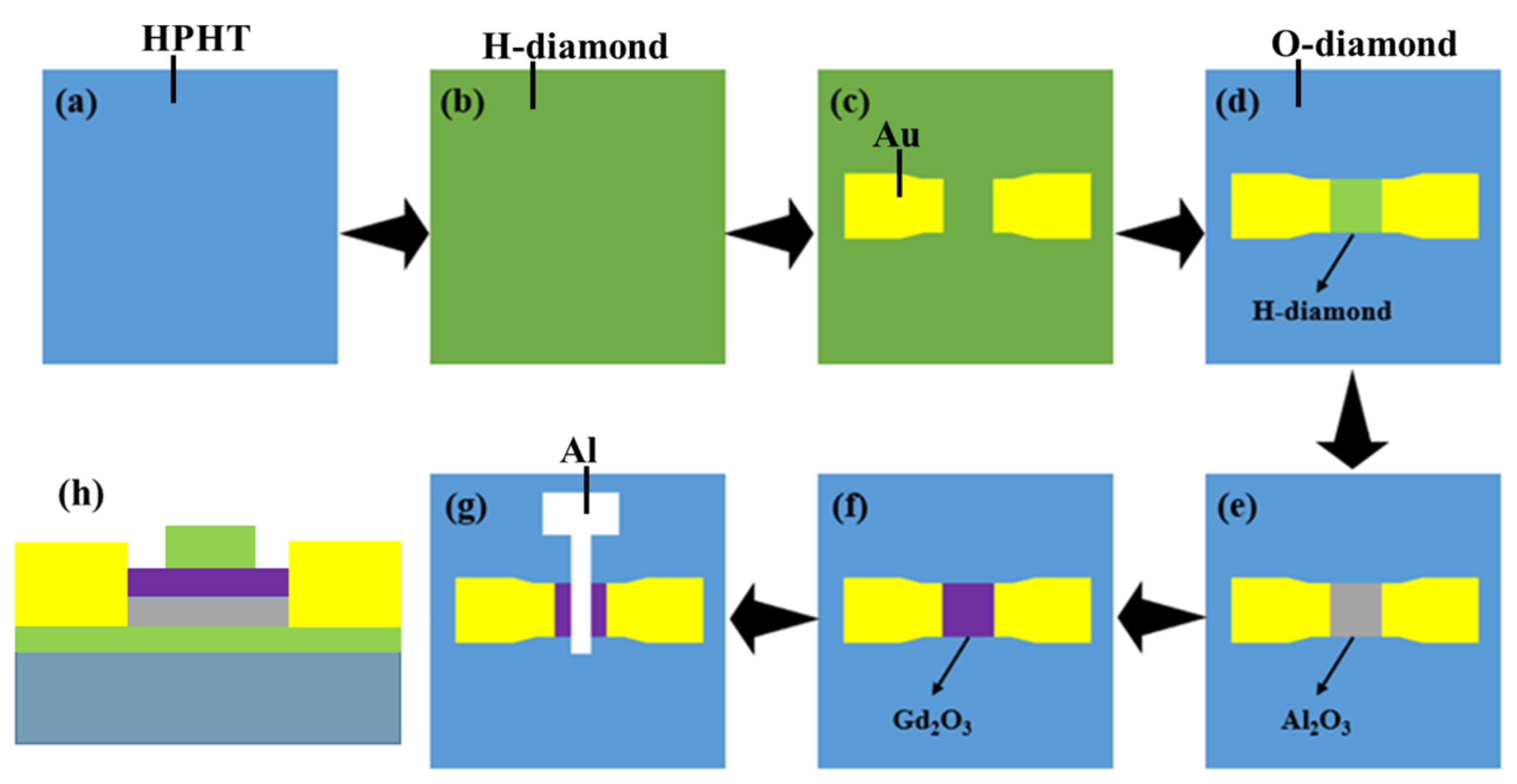
2. Material and Methods

One 3 × 3 × 0.5 mm3 high-pressure and high-temperature (HPHT) synthesized (001) single-crystal diamond was used as a substrate.
Figure 1 shows the device preparation process of Gd2O3 and Al2O3 dual dielectric layer H-diamond MOSFETs. Before this, impurities on the diamond substrate were removed by acid cleaning (H2SO4:HNO3 = 31.2:36, at 250 °C) to ensure the consistency of the device’s performance. Then, a 200 nm undoped single-crystal diamond was grown on the HPHT substrate by a microwave plasma CVD system. The methane flow rate was then set to zero and treated with hydrogen to form 2DHG, as shown in Figure 1b. Next, the source and drain images were prepared on the substrate surface by traditional photolithography. After that, a 150 nm Au film was plated on the substrate surface by electron beam deposition (EB), and a source leakage electrode was obtained by stripping, as shown in Figure 1c. The distance between the source and drain was 20 μm (LSD = 20 μm). Then, the device channel was covered with photoresist, and the sample was treated with UV/Ozone to isolate the device. After isolation, 20 nm Al2O3 was deposited using the ALD system. The precursors in the above process were water vapor and TMA. The ALD process was divided into 5 nm (80 °C) and 15 nm (250 °C) steps. Then, 52.3 nm Gd2O3 was deposited by SD at room temperature (RT), as shown in Figure 1f. The deposition pressure, power and time were 0.5 Pa, 75 W and 30 min, respectively. Finally, the 150 nm Al electrode was deposited on the device by EB, and the complete MOSFET device was finally obtained after stripping, as is shown in Figure 1g. The length (LG) and width (WG) of the gate were 20 μm and 100 μm, respectively. The section diagram of the device is shown in Figure 1h.
The electrical properties of the Gd2O3/Al2O3 H-diamond MOSFETs were investigated using an RT probe system in the air. This system has two test channels, AC and DC, and can be used for the performance testing of various electronic devices. In this work, the output characteristics, transfer characteristics, and C–V characteristics of MOSFETs were mainly tested.

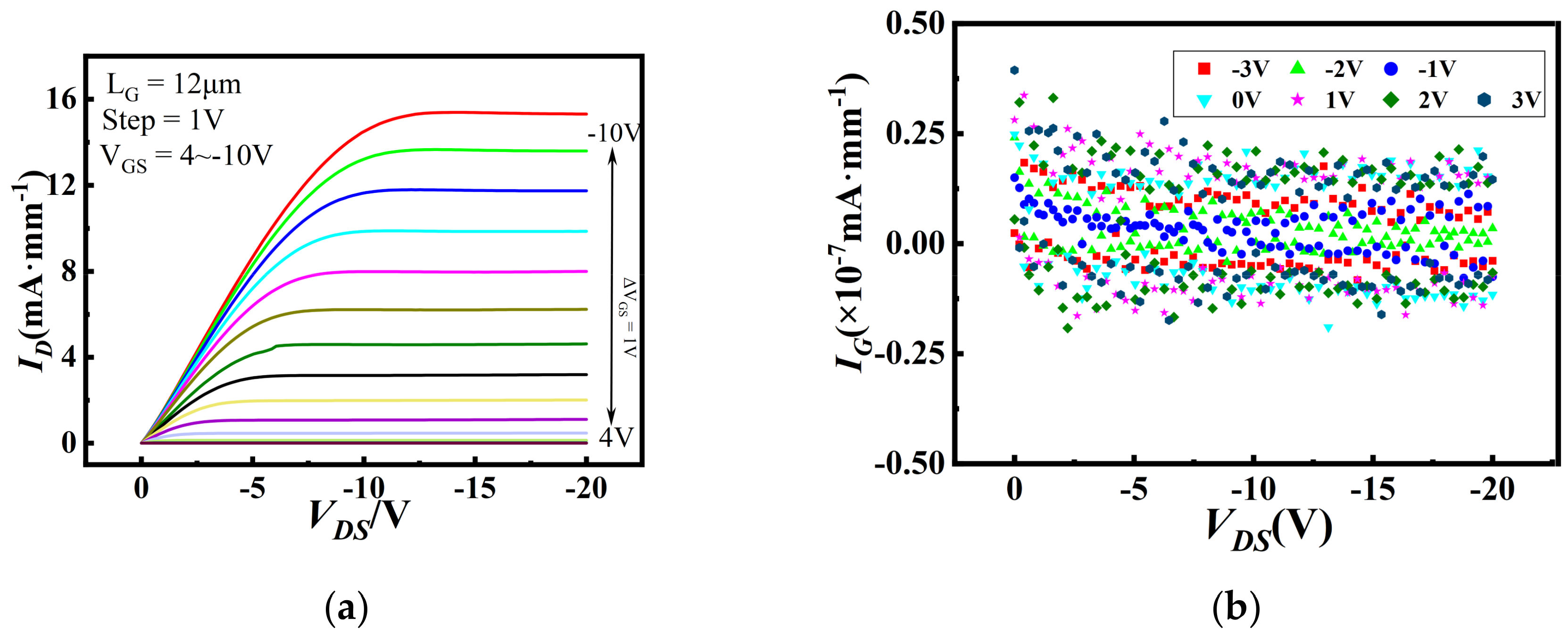
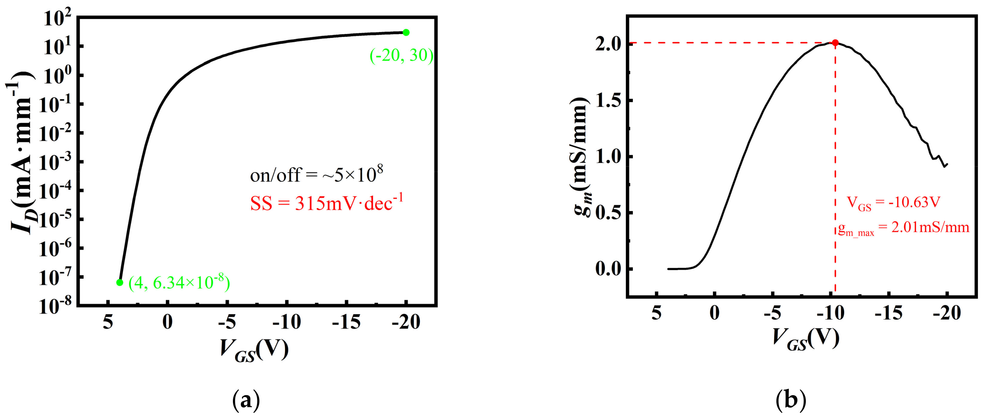
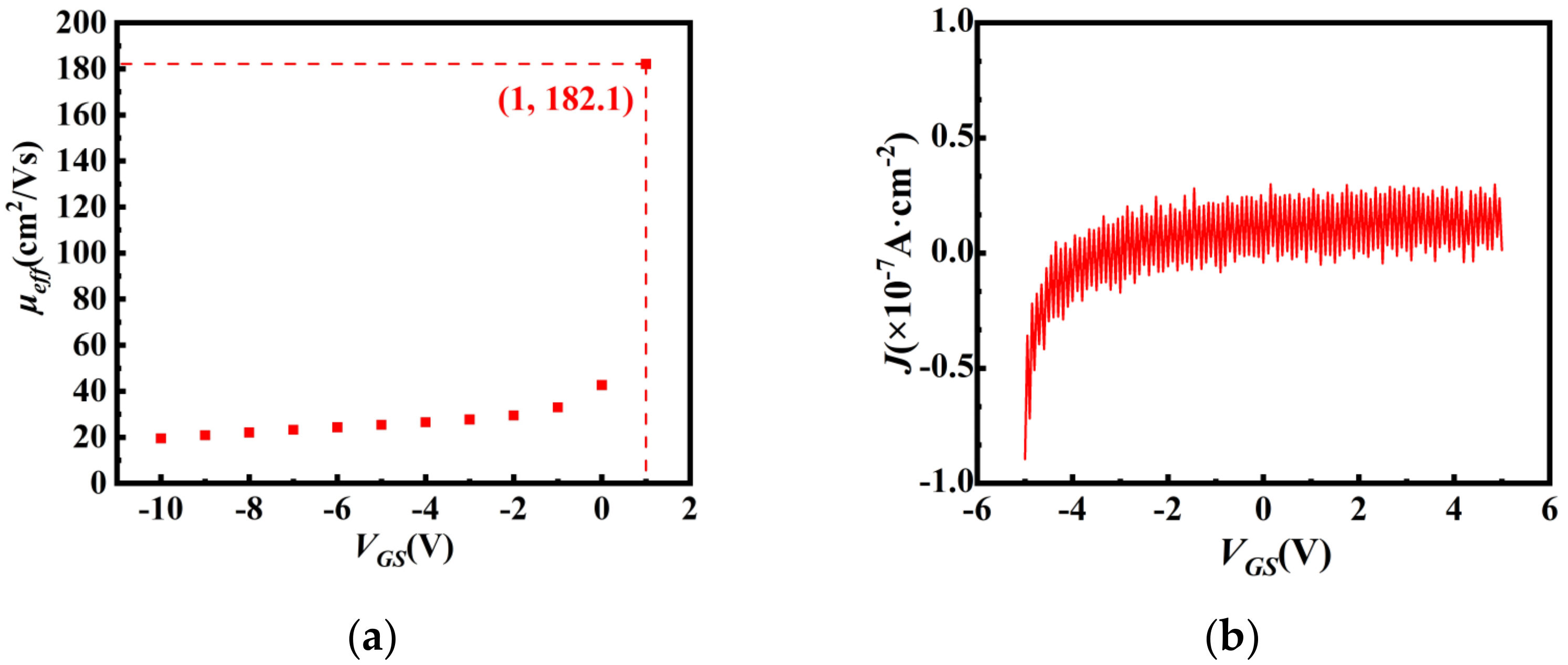
3. Results and Discussion

Figure 2a shows the output characteristics curve (ID-VGS) of the H-diamond MOSFET with Gd2O3/Al2O3 dielectric layers. In this figure, VDS varied from 0 to −20 V. The VGS was from −10 to 4 V with the step of 1 V. The device in the figure shows the characteristics of p-type MOSFET, indicating that 2DHG was successfully generated on the H-diamond. The variable resistor, as of the region and the saturation region of the MOSFET, can be clearly observed in the output characteristic curve. In the figure, we can see that the maximum current (ID) was −15.3 mA / mm at VDS = −20 V and VGS = 10 V. Figure 2b shows the current characteristics of MOS dielectric layers on the device under operating conditions at gate leakage with a source-drain voltage VDS ranging from 0 to −20 V and gate control voltage VGS from −3 to 3 V in steps of 1 V. For the MOSFET, the device gate leakage current was at a small level when the gate voltage was in the range of −3 to 3 V and between 5 × 10⁻⁸ mA/mm and −5 × 10⁻⁸ mA/mm. This meant that the current leakage from the gate to the channel in the operating state was small, and the interference to the device was small. In addition, the device had good saturation characteristics and low current jitter during testing. This indirectly indicates that the dielectric layers (Gd2O3/Al2O3) were stable, and the device had a small leakage current.
Figure 3a shows the transfer characteristic curve (ID-VGS) of the device in the logarithmic coordinate system at VDS = 10 V. In the figure, the maximum value of ID was 30 mA / mm at VGS = −20 V, and the minimum value was 6.3 × 10⁻⁸  mA / mm . Therefore, the ON/OFF ratio of this device could reach at least 5 × 10⁸. This on/off ratio was more than sufficient in practical applications. The subthreshold swing (SS) was 315 mV/dec, as extracted from Figure 3a. The subthreshold swing of the device was too large to cause the MOSFET switching rate to slow down, possibly due to poor interfacial state characteristics at the interface between the semiconductor and dielectric layers. Figure 3b shows the extrinsic transconductance (gm) versus VGS curves at VDS = 10 V. The maximum external transconductance was 2.01 mS/mm at VGS = −10.63 V.
Figure 4 shows the transfer characteristic curves of the device in linear coordinates at VDS = 10 V. Using the method in Reference [8], the threshold voltage (VTH) was 1.12 V.
Figure 5a shows the gate area capacitance–voltage (C-V) curves at a 100 KHz frequency. In the figure, the red line and the black line represent the C–V curves of the voltage when scanned from 6 to −6 V and −6 to 6 V, respectively. Both curves showed typical regions of accumulation and depletion, and 0.146   μ F / cm 2 was the maximum value of capacitance (COX). In order to more accurately calculate the dielectric constant of Gd2O3, the same process was used to prepare MOSFETs of the Al2O3 dielectric layer of the same thickness and their C–V characteristics were measured. Here, we used Equation (1) to calculate the dielectric constant:
k = Cd ε o S  
where k, d, C, ε o and S are the dielectric constant, thickness, capacitance, electrostatic force constant and area, respectively. According to Equation (1), the overall dielectric constant of the double dielectric layer was calculated to be 11.9. As for ALD-Al2O3 MOSFET, the dielectric constant (kAl2O3) was calculated as 4.9. Similarly, the dielectric constant of SD-Gd2O3 was 24.8. This value was larger than the dielectric constant of Gd2O3 (9~14), as recorded previously in the literature [24,25,26].
As shown in the blue line in Figure 5a, the flat band voltage (VFB) was calculated to be −0.62 V using the method in reference [14]. Based on this, we could calculate the flat band capacitance (CFB) to be 0.137 μF/cm2.ΔVFB is the hysteresis voltage (−0.12 V) obtained by CFB in Figure 5a. Therefore, the trapped charge densities (Qt) in SD-Gd2O3/ALD-Al2O3 could be calculated as 1.08 × 1011 cm−2 by Equation (2). The gate metal in this device was Al, and its work function was 4.28 eV. The work function of the hydrogen terminal diamond is 4.9 eV, from which the flat-band voltage (VFB0) in the ideal state was calculated to be −0.62 V. The flat-band voltage obtained using the forward capacitance voltage characteristic was 0.62 V. Using Equation (3), it could be calculated that the fixed charge density in the device was 1.04 × 1012 cm−2 and the fixed charge type was negative, which had no compensating effect on 2DHG in the hydrogen terminal diamond and was the reason behind why the device behaved normally on this type. In Figure 5a, we calculate the carrier density (p) as 7.08 × 1012 cm−2 using Equation (4), VGS = −6 V. Figure 5b shows the accumulation of the device carrier concentration with voltage.
Q t = C OX Δ V FB q  
Q f = C OX ( V FB 0 V FB 1 ) q  
p = 1 q CdV GS
Figure 6a shows the relationship between carrier mobility (μeff) and VGS. μeff was calculated by Formula (4) to be 182.1 cm 2 / Vs when VGS was 1 V. Comparing this with Figure 5b, it can be seen that as the gate voltage increased, the carrier concentration accumulated and increased, but the effective carrier mobility of the channel decreased. When the carrier concentration increased, the collision probability of the carriers in the semiconductor increased, leading to an increase in scattering and resulting in an effective carrier mobility decrease.
I D = μ eff W G C OX 2 W L V GS V TH 2
Figure 6b shows the leakage current density (J) of the sample in a logarithmic coordinate. In the figure, VGS varies from −5 V to 5 V. When the voltage changed within this range, MOSFET showed a very small leakage current. The leakage current density was basically less than 3 × 10⁻⁷ A/cm2 at VGS = −5 V and 9 × 10⁻⁷ A/cm2 at VGS = 5 V. In the figure it can be seen that when the gate voltage was −5 V, the device leakage current took the maximum value of 1 × 10⁻⁷ A/cm2. Additionally, in the other voltage ranges, the current density leaking from the gate varied from 0.5 × 10⁻⁷ A/cm2 to −0.5 × 10⁻⁷ A/cm2. The leakage current magnitude was at a better level among equivalent studies. This indicates that the insulating properties of the films prepared in this experiment using magnetron sputtering and atomic layer deposition were better.
The device in this work is a planar MOSFET, and the on-state resistance Ron of the device in the operating state could be divided into two parts: the first part was the high resistance state region covered by the gate channel, and the other part was the low resistance state part RSD not covered by the gate. The resistance of the low resistance state part was generated due to the resistance of the electrode and the hydrogen terminal diamond. The equation to calculate the effective carrier mobility (μeff) at the channel based on the on-resistance is:
R on = R Au + R h + L G W G μ eff C ox V GS V TH
The on-state resistance at each gate voltage of the device could be extracted in the unsaturated region of the output characteristic curve. For the prepared devices, the electrode resistance RAu and the hydrogen terminal diamond resistance Rh in the uncovered part were determined values, and the fixed slope value and intercept could be obtained by fitting the device with on-state resistance Ron and 1/|VGS − VTH| to calculate the effective carrier mobility of the hydrogen terminal diamond and the source-drain series resistance RSD of the device, Figure 7 shows the on-state resistance Ron and 1/|VGS − VTH| fitting relationship for MOSFET.
When fitting the part of 1/|VGS − VTH| that was linearly related to the on-resistance Ron in the range from 0 to 0.5 V−1, the fitted relations for the devices could be obtained as:
R on = 42474 × 1 V GS V TH + 1451
The effective carrier mobility of the device was extracted from the slope of the fitted straight line as 20.04 cm2/Vs, and the on-state resistance was 1451 Ω.
Finally, Table 1 shows a comparison of the parameters between this work and several previous MOSFETs, such as Al2O3 [1], HfSiO4/Al2O3 [14], YSZ/Al2O3 [23]. The devices prepared in this paper are at the normal level in the related studies [27,28,29,30,31,32,33]. Moreover, the dielectric constant of Gd2O3 is at a high level.

4. Conclusions

In summary, a MOSFET with an SD-Gd2O3/ALD-Al2O3 bilayer dielectric was successfully fabricated on a single-crystal H-diamond. The electrical properties of the MOSFET were measured at room temperature. As can be seen from the output characteristic curves, IDmax was 15.3 mA/mm at VDS = −20 V and VGS = 10 V. Based on the transfer characteristic, VTH and the on/off ratio were 1.12 V and 5 × 10⁸, respectively. In addition, the gm and the subthreshold swing of the device were 2.01 mS mm and 315 mV/dec, respectively. According to the C–V results, the trapped charge densities of the MOSFET in the gate dielectric layers was 1.08 × 1011 cm−2. The dielectric constants (k) of ALD-Al2O3 and SD-Gd2O3 were evaluated to be 4.9 and 24.8. The value of μeff was evaluated to be 182.1 cm2/Vs at VGS = 1.0 V. Furthermore, due to the stable properties of Gd2O3, the leakage current density (<1 × 10⁻⁷ A/cm2) of the MOSFET was very small.

Author Contributions

X.L. and W.W. designed the experiment. X.L., Y.W., G.C., S.H. and M.Z. finished the experiment. X.L. measured samples. X.L., Y.W. and H.W. analyze the data. X.L. write this manuscript and all authors participate in discussions. All authors have read and agreed to the published version of the manuscript.

Funding

This research was funded by the National Key Research and Development Program of China (No. 2021YFB3602100), the National Natural Science Foundation of China (No. 61627812, 61804122, 62074127 and U21A2073), the China Postdoctoral Science Foundation (No.2022M712516 and 2020M683485), and the Natural Science Basic Research Program of Shaanxi Province (No. 2023-JC-QN-0718 and No. 2023-JC-QN-0694).

Data Availability Statement

Data available on request due to restrictions e.g. privacy or ethics. The data presented in this study are available on request from the corresponding author.

Acknowledgments

This work was supported by the National Key Research and Development Program of China (No. 2021YFB3602100), the National Natural Science Foundation of China (No. 61627812, 61804122, 62074127 and U21A2073), the China Postdoctoral Science Foundation (No.2022M712516 and 2020M683485), and the Natural Science Basic Research Program of Shaanxi Province (No. 2023-JC-QN-0718 and No. 2023-JC-QN-0694).

Conflicts of Interest

The authors declare no conflict of interest.

References

  1. Saha, N.C.; Kim, S.-W.; Oishi, T.; Kawamata, Y.; Koyama, K.; Kasu, M. 345-MW/cm2 2608-V NO2 p-type Doped Diamond MOSFETs with an Al2O3 Passivation Overlayer on Heteroepitaxial Diamond. IEEE Electron Device Lett. 2021, 42, 903–906. [Google Scholar] [CrossRef]
  2. Imanishi, S.; Horikawa, K.; Oi, N.; Okubo, S.; Kageura, T.; Hiraiwa, A.; Kawarada, H. 3.8 W/mm RF Power Density for ALD Al2O3-Based Two-Dimensional Hole Gas Diamond MOSFET Operating at Saturation Velocity. IEEE Electron Device Lett. 2018, 40, 279–282. [Google Scholar] [CrossRef]
  3. Zhang, M.; Wang, W.; Chen, G.; Abbasi, H.N.; Wang, Y.; Lin, F.; Wen, F.; Wang, K.; Zhang, J.; Bu, R.; et al. Normally off hydrogen-terminated diamond field-effect transistor with Ti/TiOx gate materials. IEEE Trans. Electron Devices 2020, 67, 4784–4788. [Google Scholar] [CrossRef]
  4. Chen, G.; Wang, W.; He, S.; Wang, J.; Zhang, S.; Zhang, M.; Wang, H.-X. Leakage current reduction of normally off hydrogen-terminated diamond field effect transistor utilizing dual-barrier Schottky gate. J. Appl. Phys. 2022, 132, 015702. [Google Scholar] [CrossRef]
  5. Zhang, M.; Wang, W.; Wen, F.; Lin, F.; Chen, G.; He, S.; Wang, Y.; Fan, S.; Bu, R.; Min, T.; et al. Large VTH of Normally-off Field Effect Transistor with Yttrium Gate Material Directly Deposited on Hydrogen-Terminated Diamond. IEEE Trans. Electron Devices 2022, 69, 3563–3567. [Google Scholar] [CrossRef]
  6. Davis, R.; Sitar, Z.; Williams, B.; Kong, H.; Kim, H.; Palmour, J.; Edmond, J.; Ryu, J.; Glass, J.; Carter, C. Critical evaluation of the status of the areas for future research regarding the wide band gap semiconductors diamond, gallium nitride and silicon carbide. Mater. Sci. Eng. B 1988, 1, 77–104. [Google Scholar] [CrossRef]
  7. Fei, W.; Bi, T.; Iwataki, M.; Imanishi, S.; Kawarada, H. Oxidized Si terminated diamond and its MOSFET operation with SiO2 gate insulator. Appl. Phys. Lett. 2020, 116, 212103. [Google Scholar] [CrossRef]
  8. Wang, W.; Fu, K.; Hu, C.; Li, F.; Liu, Z.; Li, S.; Lin, F.; Fu, J.; Wang, J.; Wang, H. Diamond based field-effect transistors with SiNx and ZrO2 double dielectric layers. Diam. Relat. Mater. 2016, 69, 237–240. [Google Scholar] [CrossRef]
  9. Zhu, X.; Shao, S.; Chan, S.; Tu, J.; Ota, K.; Huang, Y.; An, K.; Chen, L.; Wei, J.; Liu, J.; et al. High Performance of Normally-on and Normally-off Devices with Highly Boron-Doped Source and Drain on H-Terminated Polycrystalline Diamond. Adv. Electron. Mater. 2023, 9, 2201122. [Google Scholar] [CrossRef]
  10. Imura, M.; Hayakawa, R.; Ohsato, H.; Watanabe, E.; Tsuya, D.; Nagata, T.; Liao, M.; Koide, Y.; Yamamoto, J.-I.; Ban, K.; et al. Development of AlN/diamond heterojunction field effect transistors. Diam. Relat. Mater. 2012, 24, 206–209. [Google Scholar] [CrossRef]
  11. Shiomi, H.; Nishibayashi, Y.; Toda, N.; Shikata, S.-I. Pulse-doped diamond p-channel metal semiconductor field-effect transistor. IEEE Electron Device Lett. 1995, 16, 36–38. [Google Scholar] [CrossRef]
  12. Aleksov, A.; Vescan, A.; Kunze, M.; Gluche, P.; Ebert, W.; Kohn, E.; Bergmeier, A.; Dollinger, G. Diamond junction FETs based on δ-doped channels. Diam. Relat. Mater. 1999, 8, 941–945. [Google Scholar] [CrossRef]
  13. Imanishi, S.; Kudara, K.; Ishiwata, H.; Horikawa, K.; Amano, S.; Iwataki, M.; Morishita, A.; Hiraiwa, A.; Kawarada, H. Drain Current Density Over 1.1 A/mm in 2D Hole Gas Diamond MOSFETs With Regrown p++-Diamond Ohmic Contacts. IEEE Electron Device Lett. 2020, 42, 204–207. [Google Scholar] [CrossRef]
  14. Hirama, K.; Sato, H.; Harada, Y.; Yamamoto, H.; Kasu, M. Diamond Field-Effect Transistors with 1.3 A/mm Drain Current Density by Al2O3 Passivation Layer. Jpn. J. Appl. Phys. 2012, 51, 090112. [Google Scholar] [CrossRef]
  15. Liu, J.W.; Liao, M.-Y.; Imura, M.; Watanabe, E.; Oosato, H.; Koide, Y. Diamond field effect transistors with a high-dielectric constant Ta2O5 as gate material. Appl. Phys. 2014, 47, 245102. Available online: http://iopscience.iop.org/0022-3727/47/24/245102 (accessed on 14 April 2023).
  16. Liu, J.; Liao, M.; Imura, M.; Tanaka, A.; Iwai, H.; Koide, Y. Low on-resistance diamond field effect transistor with high-k ZrO2 as dielectric. Sci. Rep. 2014, 4, 6395. [Google Scholar] [CrossRef]
  17. Vardi, A.; Tordjman, M.; del Alamo, J.A.; Kalish, R. A Diamond:H/MoO3 MOSFET. IEEE Electron Device Lett. 2014, 35, 1320–1322. [Google Scholar] [CrossRef]
  18. Liu, J.W.; Liao, M.Y.; Imura, M.; Koide, Y. Normally-off HfO2-gated diamond field effect transistors. Appl. Phys. Lett. 2013, 103, 092905. [Google Scholar] [CrossRef]
  19. Zhao, J.; Liu, J.; Sang, L.; Liao, M.; Coathup, D.; Imura, M.; Shi, B.; Gu, C.; Koide, Y.; Ye, H. Assembly of a high-dielectric constant thin TiOx layer directly on H-terminated semiconductor diamond. Appl. Phys. Lett. 2016, 108, 012105. [Google Scholar] [CrossRef]
  20. Liu, J.W.; Liao, M.Y.; Imura, M.; Matsumoto, T.; Shibata, N.; Ikuhara, Y.; Koide, Y. Interfacial band configuration and electrical properties of LaAlO3/Al2O3/hydrogenated-diamond metal-oxide-semiconductor field effect transistors. J. Appl. Phys. 2015, 118, 084108. [Google Scholar] [CrossRef]
  21. Liu, J.W.; Oosato, H.; Liao, M.Y.; Koide, Y. Enhancement-mode hydrogenated diamond metal-oxide-semiconductor field-effect transistors with Y2O3 oxide insulator grown by electron beam evaporator. Appl. Phys. Lett. 2017, 110, 203502. [Google Scholar] [CrossRef]
  22. Kahraman, A.; Yilmaz, E. A comprehensive study on usage of Gd2O3 dielectric in MOS based radiation sensors considering frequency dependent radiation response. Radiat. Phys. Chem. 2018, 152, 36–42. [Google Scholar] [CrossRef]
  23. Moshaev, V.; Leibin, Y.; Malka, D. Optimizations of Si PIN diode phase-shifter for controlling MZM quadrature bias point using SOI rib waveguide technology. Opt. Laser Technol. 2021, 138, 106844. [Google Scholar] [CrossRef]
  24. Omoru, E.O.; Srivastava, V.M. Testing and Analysis of MOSFET-Based Absorber Integrated Antenna for 5G/WiMAX/WLAN Applications. Nanomaterials 2022, 12, 2911. [Google Scholar] [CrossRef] [PubMed]
  25. Gupta, S.; Sachan, R.; Narayan, J. Performance of hydrogen-terminated diamond MOSFET with bilayer dielectrics of YSZ/Al2O3. Diam. Relat. Mater. 2019, 99, 107532. [Google Scholar] [CrossRef]
  26. El Kamel, F.; Gonon, P.; Vallée, C.; Jousseaume, V.; Grampeix, H. Voltage-induced recovery of dielectric breakdown (high current resistance switching) in HfO2. Appl. Phys. Lett. 2011, 98, 023504. [Google Scholar] [CrossRef]
  27. Zhang, M.; Wang, W.; Fan, S.; Chen, G.; Abbasi, H.N.; Lin, F.; Wen, F.; Zhang, J.; Bu, R.; Wang, H.-X. Normally-off hydrogen-terminated diamond field effect transistor with yttrium gate. Carbon 2021, 176, 307–312. [Google Scholar] [CrossRef]
  28. Zhang, M.; Wang, W.; Chen, G.; Abbasi, H.N.; Lin, F.; Wen, F.; Wang, K.; Zhang, J.; Bu, R.; Wang, H. Electrical properties of yttrium gate hydrogen-terminated diamond field effect transistor with Al2O3 dielectric layer. Appl. Phys. Lett. 2021, 118, 053506. [Google Scholar] [CrossRef]
  29. Chang, C.; Chen, G.; Shao, G.; Wang, Y.; Zhang, M.; Su, J.; Lin, F.; Wang, W.; Wang, H.-X. Normally-off hydrogen-terminated diamond field effect transistor with a bilayer dielectric of Er2O3/Al2O3. Diam. Relat. Mater. 2022, 123, 108848. [Google Scholar] [CrossRef]
  30. Su, K.; Ren, Z.; Peng, Y.; Zhang, J.; Zhang, J.; Zhang, Y.; He, Q.; Zhang, C.; Hao, Y. Normally-off Hydrogen-Terminated Diamond Field Effect Transistor With Ferroelectric HfZrOx/Al2O3Gate Dielectrics. IEEE Access 2020, 8, 20043–20050. [Google Scholar] [CrossRef]
  31. Wang, Y.-F.; Wang, W.; Abbasi, H.N.; Chang, X.; Zhang, X.; Zhu, T.; Liu, Z.; Song, W.; Chen, G.; Wang, H.-X. LiF/Al2O3 as Dielectrics for MOSFET on Single Crystal Hydrogen-Terminated Diamond. IEEE Electron Device Lett. 2020, 41, 808–811. [Google Scholar] [CrossRef]
  32. Shablonin, E.; Popov, A.; Prieditis, G.; Vasil’Chenko, E.; Lushchik, A. Thermal annealing and transformation of dimer F centers in neutron-irradiated Al2O3 single crystals. J. Nucl. Mater. 2020, 543, 152600. [Google Scholar] [CrossRef]
  33. Abbasi, H.N.; Wang, Y.-F.; Wang, W.; Hussain, J.; Wang, H.-X. Diamond field effect transistors using bilayer dielectrics Yb2TiO5/Al2O3 on hydrogen-terminated diamond. Diam. Relat. Mater. 2020, 106, 107866. [Google Scholar] [CrossRef]
Figure 1. (ag) Gd2O3/Al2O3 H-diamond MOSFET fabrication process; (h) The section diagram of the device.
Crystals 13 00783 g001
Figure 2. (a) The output characteristic curves of MOSFET; (b) Device gate leakage current characteristics.
Crystals 13 00783 g002
Figure 3. (a) ID-VGS in the logarithmic coordinate system at VDS = 10 V; (b) gm–VGS curve.
Crystals 13 00783 g003
Figure 4. Transfer characteristic curves in linear coordinates at VDS = 10 V.
Crystals 13 00783 g004
Figure 5. (a) The gate capacitance–voltage (C–V) curves; (b) Carrier concentration characteristic curve.
Crystals 13 00783 g005
Figure 6. (a) Effective mobility for H-diamond with Gd2O3/ Al2O3 dielectric layers; (b) The gate leakage current density.
Crystals 13 00783 g006
Figure 7. Device effective carrier mobility fitting plot.
Crystals 13 00783 g007
Table 1. Device performance comparison between this work and other works.
This WorkDielectric
Layer
Dielectric
Constant
IDmax
(mA/mm)
Carrier Density (cm−2)μeff (cm2/Vs)
This workGd2O3/Al2O324.8/4.9−15.37.08 × 1011182.1
[1]Al2O33.5−7901013150
[14]HfSiO4/Al2O39−255.4 × 1011217.7
[23]YSZ/Al2O316.1−5.5-80.4
Disclaimer/Publisher’s Note: The statements, opinions and data contained in all publications are solely those of the individual author(s) and contributor(s) and not of MDPI and/or the editor(s). MDPI and/or the editor(s) disclaim responsibility for any injury to people or property resulting from any ideas, methods, instructions or products referred to in the content.

