
Self-Adaption of the GIDL Erase Promotes Stacking More Layers in 3D NAND Flash

Abstract
:1. Introduction
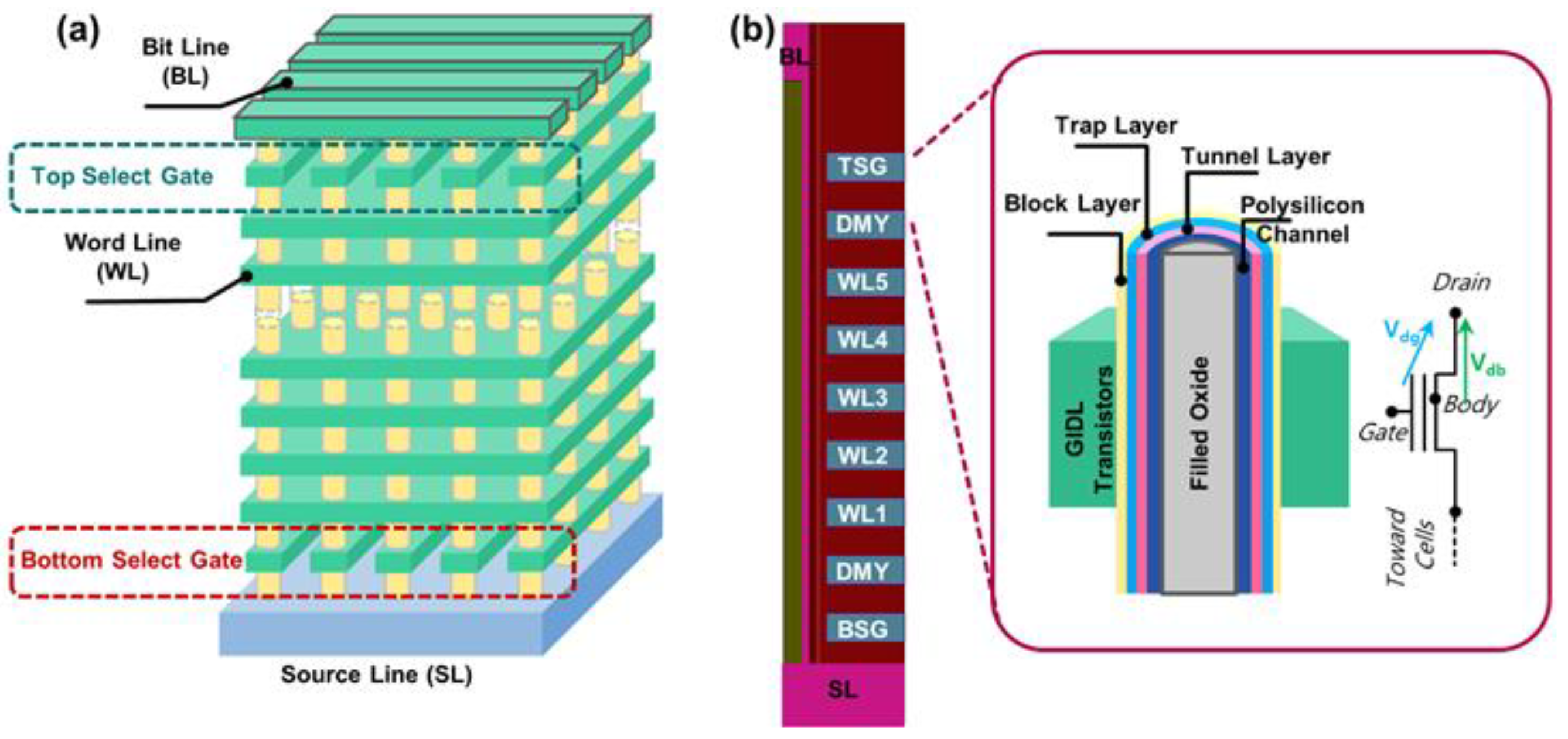
2. Simulations
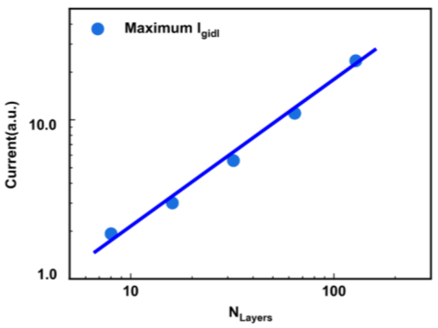
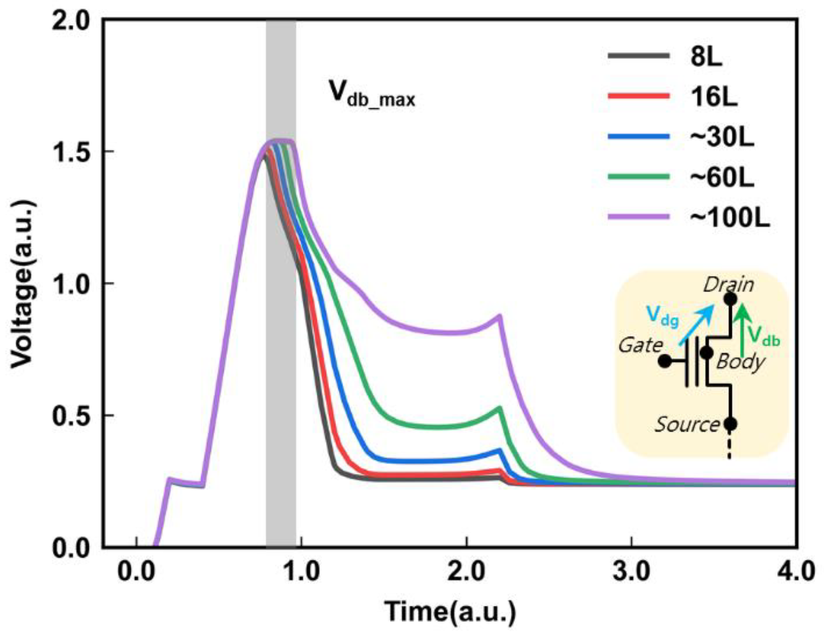
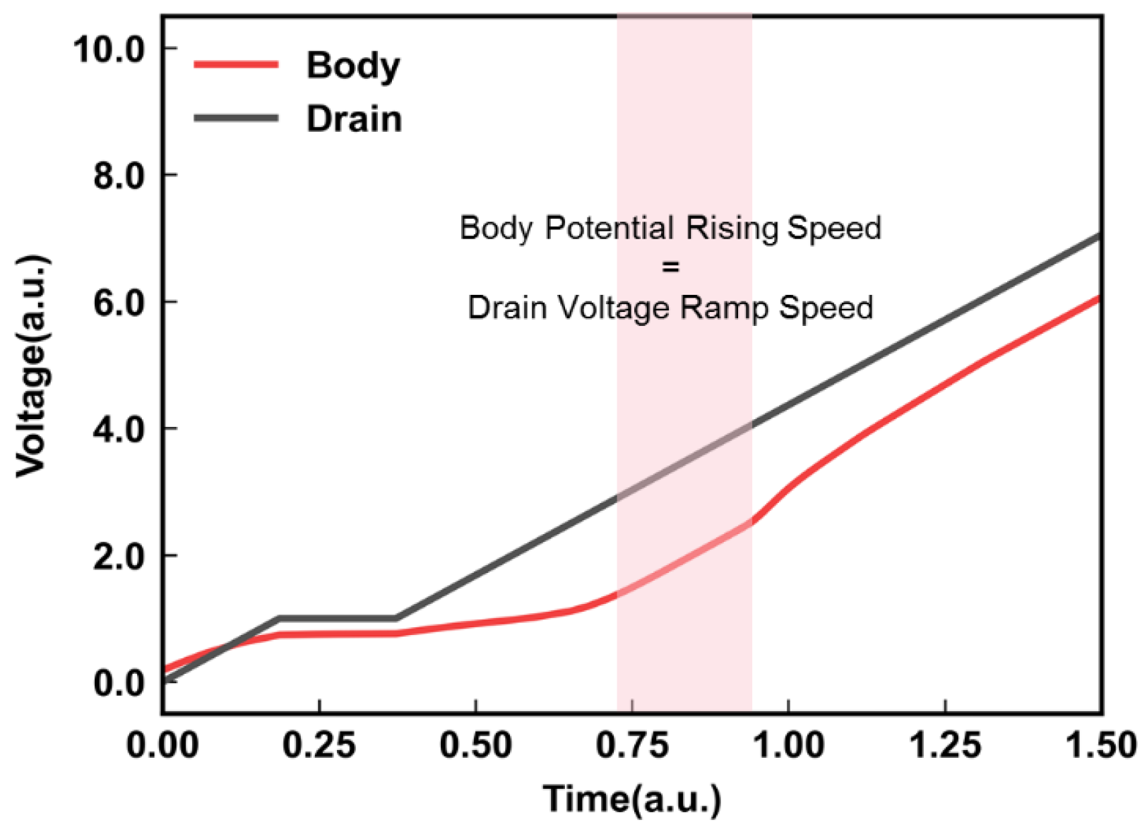
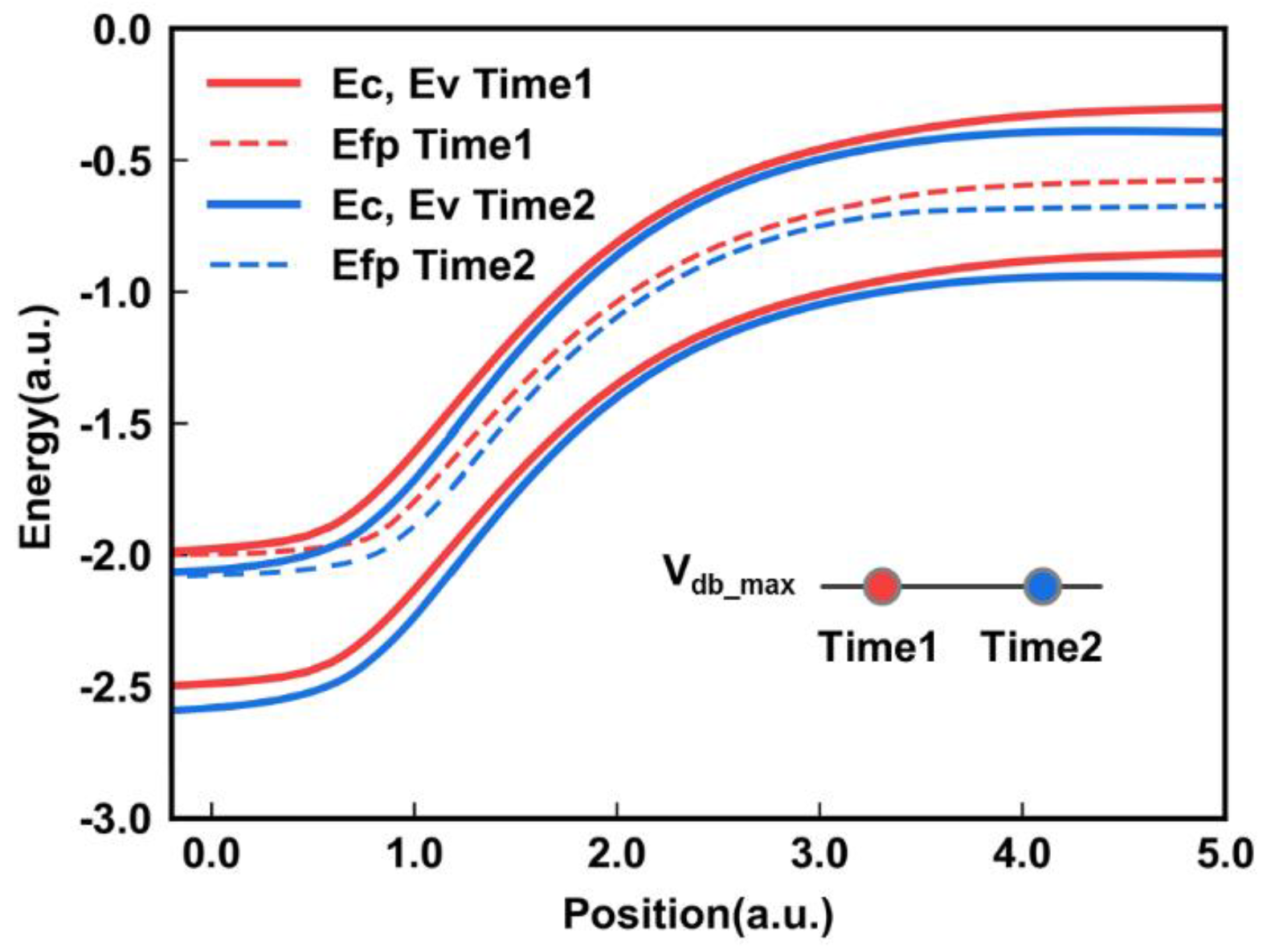
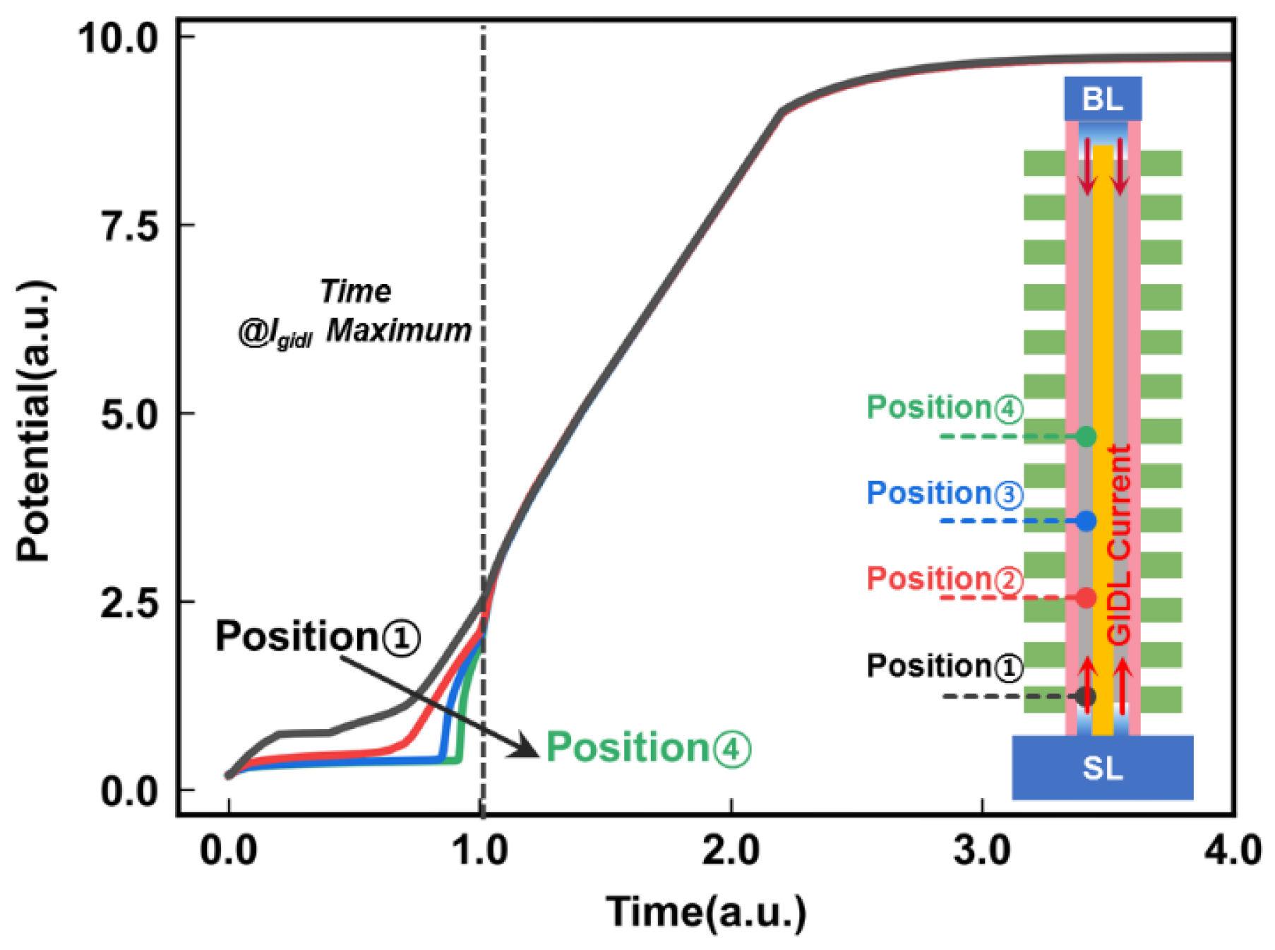
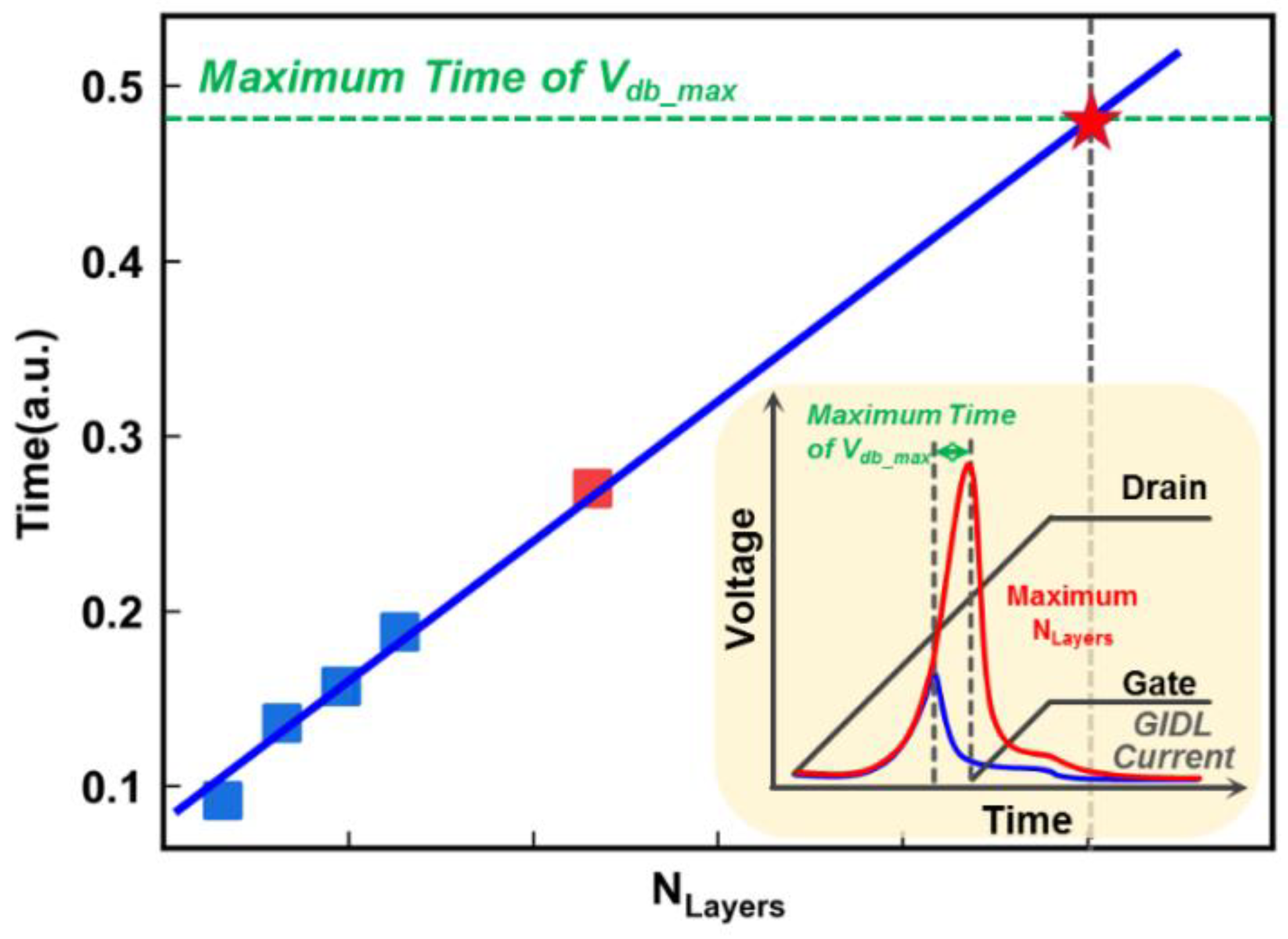
3. Results and Discussion
4. Conclusions
Author Contributions
Funding
Data Availability Statement
Conflicts of Interest
References
- Kim, C.; Cho, J.H.; Jeong, W.; Park, I.H.; Park, H.W.; Kim, D.H.; Kang, D.; Lee, S.; Lee, J.S.; Kim, W.; et al. A 512 Gb 3 b/cell 64-stacked WL 3D V-NAND flash memory. In Proceedings of the 2017 IEEE International Solid-State Circuits Conference (ISSCC), San Francisco, CA, USA, 5–9 February 2017; Volume 60, pp. 202–203. [Google Scholar]
- Maejima, H.; Kanda, K.; Fujimura, S.; Takagiwa, T.; Ozawa, S.; Sato, J.; Shindo, Y.; Sato, M.; Kanagawa, N.; Musha, J.; et al. A 512 Gb 3 b/Cell 3D flash memory on a 96-word-line-layer technology. In Proceedings of the 2018 IEEE International Solid—State Circuits Conference—(ISSCC), San Francisco, CA, USA, 11–15 February 2018; Volume 61, pp. 336–338. [Google Scholar]
- Siau, C.; Kim, K.H.; Lee, S.; Isobe, K.; Shibata, N.; Verma, K.; Ariki, T.; Li, J.; Yuh, J.; Amarnath, A.; et al. A 512 Gb 3-bit/Cell 3D Flash Memory on 128-Wordline-Layer with 132 MB/s Write Performance Featuring Circuit-Under-Array Technology. In Proceedings of the 2019 IEEE International Solid-State Circuits Conference—(ISSCC), San Francisco, CA, USA, 17–21 February 2019; pp. 218–220. [Google Scholar]
- Higuchi, T.; Kodama, T.; Kato, K.; Fukuda, R.; Tokiwa, N.; Abe, M.; Takagiwa, T.; Shimizu, Y. A 1 Tb 3 b/Cell 3D-Flash Memory in a 170+ Word-Line-Layer Technology. In Proceedings of the 2021 IEEE International Solid-State Circuits Conference (ISSCC), San Francisco, CA, USA, 13–22 February 2021; pp. 428–430. [Google Scholar]
- Park, J.; Kim, D.; Ok, S.; Park, J.; Kwon, T.; Lee, H.; Lim, S.; Jung, S.; Choi, H.; Kang, T.; et al. A 176-Stacked 512 Gb 3 b/Cell 3D-NAND Flash with 10.8 Gb/mm2 Density with a Peripheral Circuit Under Cell Array Architecture. In Proceedings of the 2021 IEEE International Solid-State Circuits Conference (ISSCC), San Francisco, CA, USA, 13–22 February 2021; pp. 422–423. [Google Scholar]
- Kim, M.; Yun, S.W.; Park, J.; Park, H.K.; Lee, J.; Kim, K.S.; Na, D.; Choi, S.; Song, Y.; Lee, J.; et al. A 1Tb 3b/Cell 8th-Generation 3D-NAND Flash Memory with 164MB/s Write Throughput and a 2.4 Gb/s Interface. In Proceedings of the 2022 IEEE International Solid-State Circuits Conference (ISSCC), San Francisco, CA, USA, 20–26 February 2022; Volume 65, pp. 136–137. [Google Scholar]
- Huo, Z.; Cheng, W.; Yang, S. Unleash Scaling Potential of 3D NAND with Innovative Xtacking® Architecture. In Proceedings of the 2022 IEEE Symposium on VLSI Technology and Circuits (VLSI Technology and Circuits), Honolulu, HI, USA, 12–17 June 2022; pp. 254–255. [Google Scholar]
- Lim, J.; Chung, S.; Ko, D.H.; Sung, S.-K.; Noh, K.; Ahn, S.J.; Song, J.H. Development of 7th generation 3D VNAND Flash Product with COP structure for Growing Demand in Storage Market. In Proceedings of the 2022 International Conference on Electronics, Information, and Communication (ICEIC), Jeju, Republic of Korea, 6–9 February 2022; pp. 1–4. [Google Scholar]
- Heineck, L.; Liu, J. 3D NAND Flash Status and Trends. In Proceedings of the 2022 IEEE International Memory Workshop (IMW), Dresden, Germany, 15–18 May 2022; pp. 1–4. [Google Scholar]
- Kang, J.; Lee, J.; Yim, Y.; Park, S.; Kim, H.S.; Cho, E.S.; Kim, T.; Lee, J.H.; Kim, J.; Lee, R.; et al. Highly Reliable Cell Characteristics with CSOB (Channel-hole Sidewall ONO Butting) Scheme for 7th Generation 3D-NAND. In Proceedings of the 2021 IEEE International Electron Devices Meeting (IEDM), San Francisco, CA, USA, 11–16 December 2021; pp. 10.1.1–10.1.4. [Google Scholar]
- Tanaka, H.; Kido, M.; Yahashi, K.; Oomura, M.; Katsumata, R.; Kito, M.; Fukuzumi, Y.; Sato, M.; Nagata, Y.; Matsuoka, Y.; et al. Bit cost scalable technology with punch and plug process for ultra high density flash memory. In Proceedings of the 2007 IEEE Symposium on VLSI Technology, Kyoto, Japan, 12–14 June 2007; pp. 14–15. [Google Scholar]
- Katsumata, R.; Kito, M.; Fukuzumi, Y.; Kido, M.; Tanaka, H.; Komori, Y.; Ishiduki, M.; Matsunami, J.; Fujiwara, T.; Nagata, Y.; et al. Pipe-shaped BiCS flash memory with 16 stacked layers and multi-level-cell operation for ultra high density storage devices. In Proceedings of the 2009 Symposium on VLSI Technology, Kyoto, Japan, 15–17 June 2009; pp. 136–137. [Google Scholar]
- Caillat, C.; Beaman, K.; Bicksler, A.; Camozzi, E.; Ghilardi, T.; Huang, G.; Liu, H.; Liu, Y.; Mao, D.; Mujumdar, S.; et al. 3DNAND GIDL-assisted body biasing for erase enabling CMOS under array (CUA) architecture. In Proceedings of the 2017 IEEE International Memory Workshop (IMW), Monterey, CA, USA, 14–17 May 2017; pp. 1–4. [Google Scholar]
- Malavena, G.; Lacaita, A.L.; Spinelli, A.S.; Compagnoni, C.M. Investigation and compact modeling of the time dynamics of the GIDL-assisted increase of the string potential in 3-D NAND flash arrays. IEEE Trans. Electron. Devices 2018, 65, 2804–2811. [Google Scholar] [CrossRef]
- Malavena, G.; Mannara, A.; Lacaita, A.L.; Spinelli, A.S.; Compagnoni, C.M. Compact modeling of GIDL-assisted erase in 3-D NAND Flash strings. J. Comput. Electron. 2019, 18, 561–568. [Google Scholar] [CrossRef]
- Kim, K. The Smallest Engine Transforming Humanity: The Past, Present, and Future. In Proceedings of the 2021 IEEE International Electron Devices Meeting (IEDM), San Francisco, CA, USA, 11–16 December 2021; pp. 1.1.1–1.1.8. [Google Scholar]
- Wang, Y.; Huang, J.; Chen, J.; Mao, R. PVSensing: A Process-Variation-Aware Space Allocation Strategy for 3D NAND Flash Memory. IEEE Trans. Comput. Aided Des. Integr. Circuits Syst. 2021, 41, 1302–1315. [Google Scholar] [CrossRef]
- Yang, T.; Xia, Z.; Shi, D.; Ouyang, Y.; Huo, Z. Analysis and optimization of threshold voltage variability by polysilicon grain size simulation in 3D NAND flash memory. IEEE J. Electron. Devices Soc. 2020, 8, 140–144. [Google Scholar] [CrossRef]


Disclaimer/Publisher’s Note: The statements, opinions and data contained in all publications are solely those of the individual author(s) and contributor(s) and not of MDPI and/or the editor(s). MDPI and/or the editor(s) disclaim responsibility for any injury to people or property resulting from any ideas, methods, instructions or products referred to in the content. |
© 2023 by the authors. Licensee MDPI, Basel, Switzerland. This article is an open access article distributed under the terms and conditions of the Creative Commons Attribution (CC BY) license (https://creativecommons.org/licenses/by/4.0/).
Share and Cite
Yang, T.; Zhang, B.; Wang, Q.; Jin, L.; Xia, Z. Self-Adaption of the GIDL Erase Promotes Stacking More Layers in 3D NAND Flash. Micromachines 2023, 14, 686. https://doi.org/10.3390/mi14030686
Yang T, Zhang B, Wang Q, Jin L, Xia Z. Self-Adaption of the GIDL Erase Promotes Stacking More Layers in 3D NAND Flash. Micromachines. 2023; 14(3):686. https://doi.org/10.3390/mi14030686
Chicago/Turabian StyleYang, Tao, Bao Zhang, Qi Wang, Lei Jin, and Zhiliang Xia. 2023. "Self-Adaption of the GIDL Erase Promotes Stacking More Layers in 3D NAND Flash" Micromachines 14, no. 3: 686. https://doi.org/10.3390/mi14030686