Next Issue
Volume 14, April
Previous Issue
Volume 14, February


Micromachines, Volume 14, Issue 3 (March 2023) – 212 articles

Cover Story (view full-size image): 
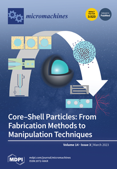
Core–shell particles are micro- or nanoparticles with solid, liquid, or gas cores encapsulated by protective solid shells. The unique composition of core and shell materials imparts smart properties on the particles. Core–shell particles are gaining increasing attention as tuneable and versatile carriers for pharmaceutical and biomedical applications including targeted drug delivery, controlled drug release, and biosensing. View this paper
  • Issues are regarded as officially published after their release is announced to the table of contents alert mailing list.
  • You may sign up for e-mail alerts to receive table of contents of newly released issues.
  • PDF is the official format for papers published in both, html and pdf forms. To view the papers in pdf format, click on the "PDF Full-text" link, and use the free Adobe Reader to open them.
Order results
Result details
Section
Select all
Export citation of selected articles as:
10 pages, 3051 KiB  
Article
Dielectrophoresis-Based Selective Droplet Extraction Microfluidic Device for Single-Cell Analysis
by Seito Shijo, Daiki Tanaka, Tetsushi Sekiguchi, Jun-ichi Ishihara, Hiroki Takahashi, Masashi Kobayashi and Shuichi Shoji
Micromachines 2023, 14(3), 706; https://doi.org/10.3390/mi14030706 - 22 Mar 2023
Viewed by 1881
Abstract
We developed a microfluidic device that enables selective droplet extraction from multiple droplet-trapping pockets based on dielectrophoresis. The device consists of a main microchannel, five droplet-trapping pockets with side channels, and drive electrode pairs appropriately located around the trapping pockets. Agarose droplets capable [...] Read more.
We developed a microfluidic device that enables selective droplet extraction from multiple droplet-trapping pockets based on dielectrophoresis. The device consists of a main microchannel, five droplet-trapping pockets with side channels, and drive electrode pairs appropriately located around the trapping pockets. Agarose droplets capable of encapsulating biological samples were successfully trapped in the trapping pockets due to the difference in flow resistance between the main and side channels. Target droplets were selectively extracted from the pockets by the dielectrophoretic force generated between the electrodes under an applied voltage of 500 V. During their extraction from the trapping pockets, the droplets and their contents were exposed to an electric field for 400–800 ms. To evaluate whether the applied voltage could potentially damage the biological samples, the growth rates of Escherichia coli cells in the droplets, with and without a voltage applied, were compared. No significant difference in the growth rate was observed. The developed device enables the screening of encapsulated single cells and the selective extraction of target droplets. Full article
(This article belongs to the Special Issue Active Colloidal and Micro Systems for Propulsion and Manipulation)
Show Figures

Figure 1

12 pages, 3063 KiB  
Article
A Multi-Label Detection Deep Learning Model with Attention-Guided Image Enhancement for Retinal Images
by Zhenwei Li, Mengying Xu, Xiaoli Yang, Yanqi Han and Jiawen Wang
Micromachines 2023, 14(3), 705; https://doi.org/10.3390/mi14030705 - 22 Mar 2023
Cited by 1 | Viewed by 1734
Abstract
At present, multi-disease fundus image classification tasks still have the problems of small data volumes, uneven distributions, and low classification accuracy. In order to solve the problem of large data demand of deep learning models, a multi-disease fundus image classification ensemble model based [...] Read more.
At present, multi-disease fundus image classification tasks still have the problems of small data volumes, uneven distributions, and low classification accuracy. In order to solve the problem of large data demand of deep learning models, a multi-disease fundus image classification ensemble model based on gradient-weighted class activation mapping (Grad-CAM) is proposed. The model uses VGG19 and ResNet50 as the classification networks. Grad-CAM is a data augmentation module used to obtain a network convolutional layer output activation map. Both the augmented and the original data are used as the input of the model to achieve the classification goal. The data augmentation module can guide the model to learn the feature differences of lesions in the fundus and enhance the robustness of the classification model. Model fine tuning and transfer learning are used to improve the accuracy of multiple classifiers. The proposed method is based on the RFMiD (Retinal Fundus Multi-Disease Image Dataset) dataset, and an ablation experiment was performed. Compared with other methods, the accuracy, precision, and recall of this model are 97%, 92%, and 81%, respectively. The resulting activation graph shows the areas of interest for model classification, making it easier to understand the classification network. Full article
(This article belongs to the Section E:Engineering and Technology)
Show Figures

Figure 1

15 pages, 2423 KiB  
Article
Robust, Superhydrophobic Aluminum Fins with Excellent Mechanical Durability and Self-Cleaning Ability
by Wenbo Su, Xiangyou Lu, Yunxiang Shu, Xianshuang Liu, Wen Gao, Jianjie Yao, Zhuang Niu and Yuanlai Xie
Micromachines 2023, 14(3), 704; https://doi.org/10.3390/mi14030704 - 22 Mar 2023
Cited by 8 | Viewed by 1162
Abstract
The self-cleaning ability of superhydrophobic metal surfaces has attracted extensive attention. The preparation of superhydrophobic material using the coating method is a common processing method. In this experiment, aluminum fins were processed by laser etching and perfluorinated two-step coating. The aluminum surface was [...] Read more.
The self-cleaning ability of superhydrophobic metal surfaces has attracted extensive attention. The preparation of superhydrophobic material using the coating method is a common processing method. In this experiment, aluminum fins were processed by laser etching and perfluorinated two-step coating. The aluminum surface was modified using a femtosecond laser and 1H,1H,2H,2H- perfluorooctane triethoxysilane (PFOTES). A superhydrophobic aluminum surface with excellent mechanical stability and self-cleaning properties was obtained with the superhydrophobic contact angle (WCA) of 152.8° and the rolling angle (SA) of 0.6°. The results show that the superhydrophobic surface has an excellent cleaning effect compared with an ordinary surface in unit time. Then, a wear resistance test of the superhydrophobic surface was carried out by using the physical wear method. The results show that physical wear had a low influence on the hydrophobic property of the specimen surface. Finally, the Vickers hardness analysis found that the superhydrophobic surface hardness was significantly better than the ordinary surface hardness compared with the superhydrophobic surface hardness. Based on the excellent self-cleaning properties, wear resistance, and robustness of superhydrophobic materials, the laser-etched and perfluorinated superhydrophobic aluminum fins designed and manufactured in this study have broad application prospects in improving the heat transfer efficiency of finned heat exchangers. Full article
Show Figures

Figure 1

20 pages, 3427 KiB  
Article
Molecular Dynamics Simulation Study on the Influence of the Abrasive Flow Process on the Cutting of Iron-Carbon Alloys (α-Fe)
by Junye Li, Zhenguo Zhao, Junwei Li, Fujun Xiao, Rongxian Qiu, Hongcai Xie and Wenqing Meng
Micromachines 2023, 14(3), 703; https://doi.org/10.3390/mi14030703 - 22 Mar 2023
Cited by 2 | Viewed by 1265
Abstract
The plastic deformation behavior and microstructural changes in workpieces during ultra-precision machining have piqued the interest of many researchers. In this study, a molecular dynamics simulation of nano-cutting iron-carbon alloy (α-Fe) is established to investigate the effects of the fluid medium and cutting [...] Read more.
The plastic deformation behavior and microstructural changes in workpieces during ultra-precision machining have piqued the interest of many researchers. In this study, a molecular dynamics simulation of nano-cutting iron-carbon alloy (α-Fe) is established to investigate the effects of the fluid medium and cutting angle on workpiece temperature, friction coefficient, workpiece surface morphology, and dislocation evolution by constructing a molecular model of C12H26 as a fluid medium in the liquid phase using an innovative combined atomic approach. It is demonstrated that the presence of the fluid phase reduces the machining temperature and the friction coefficient. The cutting angle has a significant impact on the formation of the workpiece’s surface profile and the manner in which the workpiece’s atoms are displaced. When the cutting angle is 0°, 5°, or 10°, the workpiece’s surface morphology flows to both sides in a 45° direction, and the height of atomic accumulation on the workpiece surface gradually decreases while the area of displacement changes increases. The depth of cut increases as the cutting angle increases, causing greater material damage, and the presence of a fluid medium reduces this behavior. A dislocation reaction network is formed by the presence of more single and double-branched structures within the workpiece during the cutting process. The presence of a fluid medium during large-angle cutting reduces the number of dislocations and the total dislocation length. The total length of dislocations inside the workpiece is shorter for small angles of cutting, but the effect of the fluid medium is not very pronounced. Therefore, small cutting angles and the presence of fluid media reduce the formation of defective structures within the workpiece and ensure the machining quality. Full article
(This article belongs to the Special Issue Frontiers in Ultra-Precision Machining, Volume II)
Show Figures

Figure 1

11 pages, 5861 KiB  
Article
A Piezoelectric MEMS Speaker with a Combined Function of a Silent Alarm
by Qi Wang, Tao Ruan, Qingda Xu, Zhiyong Hu, Bin Yang, Minmin You, Zude Lin and Jingquan Liu
Micromachines 2023, 14(3), 702; https://doi.org/10.3390/mi14030702 - 22 Mar 2023
Cited by 1 | Viewed by 2011
Abstract
To explore the versatility of speakers, a piezoelectric micro-electro-mechanical system (MEMS) speaker combining the function of a silent alarm is proposed, which mainly comprises a lead zirconate titanate (PZT) actuation layer and a rigid–flexible coupling supporting layer. Measurements performed on encapsulated prototypes mounted [...] Read more.
To explore the versatility of speakers, a piezoelectric micro-electro-mechanical system (MEMS) speaker combining the function of a silent alarm is proposed, which mainly comprises a lead zirconate titanate (PZT) actuation layer and a rigid–flexible coupling supporting layer. Measurements performed on encapsulated prototypes mounted to an artificial ear simulator have revealed that, compared to a speaker with a rigid supporting layer, the sound pressure level (SPL) of the proposed piezoelectric MEMS speaker with a rigid–flexible coupling supporting layer is significantly higher and is especially higher by 4.1–20.1 dB in the frequency range from 20 Hz to 4.2 kHz, indicating that the rigid–flexible coupling supporting layer can improve the SPL significantly in low frequency. Moreover, the spectral distribution characteristic of its playback audio is similar to that of the commercial electromagnetic type. The device can also function as a silent alarm based on oral airflows in dangerous situations, as it performs well at recognizing words according to their unique voltage-signal characteristics, and can avoid the effects of external sound noise, body movement, long distance, and occlusion. This strategy provides inspiration for functional diversification of piezoelectric MEMS speakers. Full article
Show Figures

Figure 1

12 pages, 3390 KiB  
Article
Application of Micro-Arc Discharges during Anodization of Tantalum for Synthesis of Photocatalytic Active Ta2O5 Coatings
by Stevan Stojadinović, Nenad Radić and Rastko Vasilić
Micromachines 2023, 14(3), 701; https://doi.org/10.3390/mi14030701 - 22 Mar 2023
Cited by 4 | Viewed by 1200
Abstract
Ta2O5 coatings were created using micro-arc discharges (MDs) during anodization on a tantalum substrate in a sodium phosphate electrolyte (10 g/L Na3PO4·10H2O). During the process, the size of MDs increases while the number of [...] Read more.
Ta2O5 coatings were created using micro-arc discharges (MDs) during anodization on a tantalum substrate in a sodium phosphate electrolyte (10 g/L Na3PO4·10H2O). During the process, the size of MDs increases while the number of MDs decreases. The elements and their ionization states present in MDs were identified using optical emission spectroscopy. The hydrogen Balmer line Hβ shape analysis revealed the presence of two types of MDs, with estimated electron number densities of around 1.1 × 10²¹ m−3 and 7.3 × 10²¹ m−3. The effect of MDs duration on surface morphology, phase and chemical composition, optical absorption, and photoluminescent, properties of Ta2O5 coatings, as well as their applications in photocatalytic degradation of methyl orange, were investigated. The created coatings were crystalline and were primarily composed of Ta2O5 orthorhombic phase. Since Ta2O5 coatings feature strong absorption in the ultraviolet light region below 320 nm, their photocatalytic activity is very high and increases with the time of the MDs process. This was associated with an increase of oxygen vacancy defects in coatings formed during the MDs, which was confirmed by photoluminescent measurements. The photocatalytic activity after 8 h of irradiation was around 69%, 74%, 80%, and 88% for Ta2O5 coatings created after 3 min, 5 min, 10 min, and 15 min, respectively. Full article
(This article belongs to the Special Issue Micro-Discharges)
Show Figures

Figure 1

19 pages, 5864 KiB  
Article
Aluminum Nitride Out-of-Plane Piezoelectric MEMS Actuators
by Almur A. S. Rabih, Mohammad Kazemi, Michaël Ménard and Frederic Nabki
Micromachines 2023, 14(3), 700; https://doi.org/10.3390/mi14030700 - 22 Mar 2023
Cited by 5 | Viewed by 1950
Abstract
Integrating microelectromechanical systems (MEMS) actuators with low-loss suspended silicon nitride waveguides enables the precise alignment of these waveguides to other photonic integrated circuits (PICs). This requires both in-plane and out-of-plane actuators to ensure high-precision optical alignment. However, most current out-of-plane electrostatic actuators are [...] Read more.
Integrating microelectromechanical systems (MEMS) actuators with low-loss suspended silicon nitride waveguides enables the precise alignment of these waveguides to other photonic integrated circuits (PICs). This requires both in-plane and out-of-plane actuators to ensure high-precision optical alignment. However, most current out-of-plane electrostatic actuators are bulky, while electrothermal actuators consume high power. Thus, piezoelectric actuators, thanks to their moderate actuation voltages and low power consumption, could be used as alternatives. Furthermore, piezoelectric actuators can provide displacements in two opposite directions. This study presents a novel aluminum nitride-based out-of-plane piezoelectric MEMS actuator equipped with a capacitive sensing mechanism to track its displacement. This actuator could be integrated within PICs to align different chips. Prototypes of the device were tested over the range of ±60 V, where they provided upward and downward displacements, and achieved a total average out-of-plane displacement of 1.30 ± 0.04 μm. Capacitance measurement showed a linear relation with the displacement, where at −60 V, the average change in capacitance was found to be −13.10 ± 0.89 fF, whereas at 60 V the change was 11.09 ± 0.73 fF. This study also investigates the effect of the residual stress caused by the top metal electrode, on the linearity of the displacement–voltage relation. The simulation predicts that the prototype could be modified to accommodate waveguide routing above it without affecting its performance, and it could also incorporate in-plane lateral actuators. Full article
Show Figures

Figure 1

17 pages, 4208 KiB  
Article
Fabrication of Chemofluidic Integrated Circuits by Multi-Material Printing
by Alexander Kutscher, Paula Kalenczuk, Mohammed Shahadha, Stefan Grünzner, Franziska Obst, Denise Gruner, Georgi Paschew, Anthony Beck, Steffen Howitz and Andreas Richter
Micromachines 2023, 14(3), 699; https://doi.org/10.3390/mi14030699 - 22 Mar 2023
Viewed by 1648
Abstract
Photolithographic patterning of components and integrated circuits based on active polymers for microfluidics is challenging and not always efficient on a laboratory scale using the traditional mask-based fabrication procedures. Here, we present an alternative manufacturing process based on multi-material 3D printing that can [...] Read more.
Photolithographic patterning of components and integrated circuits based on active polymers for microfluidics is challenging and not always efficient on a laboratory scale using the traditional mask-based fabrication procedures. Here, we present an alternative manufacturing process based on multi-material 3D printing that can be used to print various active polymers in microfluidic structures that act as microvalves on large-area substrates efficiently in terms of processing time and consumption of active materials with a single machine. Based on the examples of two chemofluidic valve types, hydrogel-based closing valves and PEG-based opening valves, the respective printing procedures, essential influencing variables and special features are discussed, and the components are characterized with regard to their properties and tolerances. The functionality of the concept is demonstrated by a specific chemofluidic chip which automates an analysis procedure typical of clinical chemistry and laboratory medicine. Multi-material 3D printing allows active-material devices to be produced on chip substrates with tolerances comparable to photolithography but is faster and very flexible for small quantities of up to about 50 chips. Full article
(This article belongs to the Special Issue Biomedical Microdevices: State of the Art and Trends)
Show Figures

Figure 1

11 pages, 15821 KiB  
Article
Detection of In-Plane Movement in Electrically Actuated Microelectromechanical Systems Using a Scanning Electron Microscope
by Tarmo Nieminen, Nikhilendu Tiwary, Glenn Ross and Mervi Paulasto-Kröckel
Micromachines 2023, 14(3), 698; https://doi.org/10.3390/mi14030698 - 22 Mar 2023
Cited by 1 | Viewed by 1636
Abstract
The measurement of in-plane motion in microelectromechanical systems (MEMS) is a challenge for existing measurement techniques due to the small size of the moving devices and the low amplitude of motion. This paper studied the possibility of using images obtained using a scanning [...] Read more.
The measurement of in-plane motion in microelectromechanical systems (MEMS) is a challenge for existing measurement techniques due to the small size of the moving devices and the low amplitude of motion. This paper studied the possibility of using images obtained using a scanning electron microscope (SEM) together with existing motion detection algorithms to characterize the motion of MEMS. SEM imaging has previously been used to detect motion in MEMS device. However, the differences in how SEM imaging and optical imaging capture motion, together with possible interference caused by electrical actuation, create doubts about how accurately motion could be detected in a SEM. In this work, it is shown that existing motion detection algorithms can be used to detect movement with an amplitude of 69 nm. In addition, the properties of SEM images, such as bright edges, complement these algorithms. Electrical actuation was found to cause error in the measurement, however, the error was limited to regions that were electrically connected to the actuating probes and minimal error could be detected in regions that were electrically insulated from the probes. These results show that an SEM is a powerful tool for characterizing low amplitude motion and electrical contacts in MEMS and allow for the detection of motion under 100 nm in amplitude. Full article
(This article belongs to the Topic MEMS Sensors and Resonators)
Show Figures

Figure 1

15 pages, 3498 KiB  
Article
Research on IMU Calibration Model Based on Polar Decomposition
by Guiling Zhao, Maolin Tan, Xu Wang, Weidong Liang, Shuai Gao and Zhijian Chen
Micromachines 2023, 14(3), 697; https://doi.org/10.3390/mi14030697 - 21 Mar 2023
Cited by 1 | Viewed by 1420
Abstract
As an important deterministic error of the inertial measurement unit (IMU), the installation error has a serious impact on the navigation accuracy of the strapdown inertial navigation system (SINS). The impact becomes more severe in a highly dynamic application environment. This paper proposes [...] Read more.
As an important deterministic error of the inertial measurement unit (IMU), the installation error has a serious impact on the navigation accuracy of the strapdown inertial navigation system (SINS). The impact becomes more severe in a highly dynamic application environment. This paper proposes a new IMU calibration model based on polar decomposition. Using the new model, the installation error is decomposed into a nonorthogonal error and a misalignment error. The compensation of the IMU calibration model is decomposed into two steps. First, the nonorthogonal error is compensated, and then the misalignment error is compensated. Based on the proposed IMU calibration model, we used a three-axis turntable to calibrate three sets of strapdown inertial navigation systems (SINS). The experimental results show that the misalignment errors are larger than the nonorthogonal errors. Based on the experimental results, this paper proposes a new method to simplify the installation error. This simplified method defines the installation error matrix as an antisymmetric matrix composed of three misalignment errors. The navigation errors caused by the proposed simplified calibration model are compared with the navigation errors caused by the traditional simplified calibration model. The 48-h navigation experiment results show that the proposed simplified calibration model is superior to the traditional simplified calibration model in attitude accuracy, velocity accuracy, and position accuracy. Full article
Show Figures

Figure 1

13 pages, 3844 KiB  
Article
A Novel Analog Interpolation Method for Heterodyne Laser Interferometer
by Chung-Ping Chang, Syuan-Cheng Chang, Yung-Cheng Wang and Pin-Yi He
Micromachines 2023, 14(3), 696; https://doi.org/10.3390/mi14030696 - 21 Mar 2023
Cited by 1 | Viewed by 1263
Abstract
Laser interferometer technology is used in the precision positioning stage as an encoder. For better resolution, laser interferometers usually work with interpolation devices. According to the interpolation factor, these devices can convert an orthogonal sinusoidal signal into several square-wave signals via digital processing. [...] Read more.
Laser interferometer technology is used in the precision positioning stage as an encoder. For better resolution, laser interferometers usually work with interpolation devices. According to the interpolation factor, these devices can convert an orthogonal sinusoidal signal into several square-wave signals via digital processing. The bandwidth of the processing will be the limitation of the moving speed of the positioning stage. Therefore, the user needs to make a trade-off between the interpolation factor and the moving speed. In this investigation, a novel analog interpolation method for a heterodyne laser interferometer has been proposed. This method is based on the principle of the lock-in amplifier (LIA). By using the proposed interpolation method, the bandwidth of the laser encoder system can be independent of the interpolation factor. This will be a significant benefit for the ultra-high resolution encoder system and the laser interferometers. The concept, design, and experiment are revealed in this manuscript. The experimental results show that the proposed interpolation method can reach nanometer resolution with a heterodyne laser interferometer, and the bandwidth of the signal is independent of the resolution. Full article
(This article belongs to the Special Issue Precision Mechatronics: Design, Control and Applications)
Show Figures

Figure 1

14 pages, 6206 KiB  
Article
Research on MEMS Solid-State Fuse Logic Control Chip Based on Electrical Explosion Effect
by Wenting Su, Wenzhong Lou, Hengzhen Feng, Yuecen Zhao, Sining Lv, Wenxing Kan and Bo He
Micromachines 2023, 14(3), 695; https://doi.org/10.3390/mi14030695 - 21 Mar 2023
Cited by 1 | Viewed by 1116
Abstract
A microelectromechanical systems (MEMS) solid-state logic control chip with three layers—diversion layer, control layer, and substrate layer—is designed to satisfy fuse miniaturization and integration requirements. A mathematical model is established according to the heat conduction equation, and the limit conditions of different structures [...] Read more.
A microelectromechanical systems (MEMS) solid-state logic control chip with three layers—diversion layer, control layer, and substrate layer—is designed to satisfy fuse miniaturization and integration requirements. A mathematical model is established according to the heat conduction equation, and the limit conditions of different structures are presented. The finite element multi-physical field simulation method is used to simulate the size and the action voltage of the diversion layer of the control chip. Based on the surface silicon process, fuse processing, and testing with the MEMS solid-state fuse-logic control chip, a diversion layer constant current, maximum current resistance test, and a control layer of different bridge area sizes, the bridge area size is 200 × 30 μm, and the minimum electrical explosion voltage is 23.6 V. The theoretical calculation results at 20 V and 100 μF demonstrate that the capacitor energy is insufficient to support the complete vaporization of the bridge area, but can be partially vaporized, consistent with the experimental results. Full article
Show Figures

Figure 1

12 pages, 19218 KiB  
Article
Acid-Base and Photocatalytic Properties of the CeO2-Ag Nanocomposites
by Alexander A. Kravtsov, Andrey V. Blinov, Andrey A. Nagdalian, Alexey A. Gvozdenko, Alexey B. Golik, Maxim A. Pirogov, Maxim A. Kolodkin, Naiyf S. Alharbi, Shine Kadaikunnan, Muthu Thiruvengadam and Mohammad Ali Shariati
Micromachines 2023, 14(3), 694; https://doi.org/10.3390/mi14030694 - 21 Mar 2023
Cited by 1 | Viewed by 1073
Abstract
In this work, CeO2 nanoparticles, as well as CeO2 nanocomposites with plasmonic silver nanoparticles, were synthesized using a simple sol-gel process. The concentration of silver in the composites varied from 0.031–0.25 wt%. Cerium hydroxide dried gel was calcined at temperatures from [...] Read more.
In this work, CeO2 nanoparticles, as well as CeO2 nanocomposites with plasmonic silver nanoparticles, were synthesized using a simple sol-gel process. The concentration of silver in the composites varied from 0.031–0.25 wt%. Cerium hydroxide dried gel was calcined at temperatures from 125 to 800 °C to obtain CeO2. It was shown that, at an annealing temperature of 650 °C, single-phase CeO2 nanopowders with an average particle size in the range of 10–20 nm can be obtained. The study of acid-base properties showed that with an increase in the calcination temperature from 500 to 650 °C, the concentration of active centers with pKa 9.4 and 6.4 sharply increases. An analysis of the acid-base properties of CeO2-Ag nanocomposites showed that with an increase in the silver concentration, the concentration of centers with pKa 4.1 decreases, and the number of active centers with pKa 7.4 increases. In a model experiment on dye photodegradation, it was shown that the resulting CeO2 and CeO2-Ag nanopowders have photocatalytic activity. CeO2-Ag nanocomposites, regardless of the silver concentration, demonstrated better photocatalytic activity than pure nanosized CeO2. Full article
Show Figures

Figure 1

4 pages, 176 KiB  
Editorial
Editorial for the Special Issue on Droplet-Based Microfluidics: Design, Fabrication, and Applications
by Pingan Zhu
Micromachines 2023, 14(3), 693; https://doi.org/10.3390/mi14030693 - 21 Mar 2023
Viewed by 1098
Abstract
Microfluidics is a rapidly growing field of research that involves the manipulation and analysis of fluids in small-scale channels, usually with dimensions ranging from sub-micrometer to sub-millimeter [...] Full article
(This article belongs to the Special Issue Droplet-Based Microfluidics: Design, Fabrication and Applications)
12 pages, 5833 KiB  
Article
Multilayer Smart Holographic Label with Integrated RFID for Product Security and Monitoring
by Cătălin Pârvulescu, Veronica Anăstăsoaie, Roxana Tomescu, Martino Aldrigo and Dana Cristea
Micromachines 2023, 14(3), 692; https://doi.org/10.3390/mi14030692 - 21 Mar 2023
Viewed by 1825
Abstract
Counterfeiting presents a major economic problem and an important risk for the public health and safety of individuals and countries. To make the counterfeiting process more difficult, and to ensure efficient authentication, a solution would be to attach anti-counterfeit labels that include a [...] Read more.
Counterfeiting presents a major economic problem and an important risk for the public health and safety of individuals and countries. To make the counterfeiting process more difficult, and to ensure efficient authentication, a solution would be to attach anti-counterfeit labels that include a radio frequency identification (RFID) element to the products. This can allow real-time quality check along the entire supply chain. In this paper we present the technology optimized to obtain a multilayer holographic label with a high degree of security, patterned on a thin zinc sulfide film of a semi-transparent holographic foil rather than on the standard substrate for diffractive optical elements (metallized foil). The label is applied onto the product surface or packaging for anti-counterfeit protection. The developed multilayer structure contains various elements such as: a holographic background, nanotext-type elements, holographic elements, and an RFID antenna. The employed semi-transparent holographic foil offers the RFID antenna the possibility to transmit the electromagnetic signal through the label and thus to maximize the antenna footprint, achieving up to 10 m reading distance, with a 6 cm × 6 cm label, much smaller than the commercial standard (minimum 10 cm × 10 cm). Full article
(This article belongs to the Special Issue Novel Developments in Waveguides and Antennas)
Show Figures

Figure 1

21 pages, 9457 KiB  
Review
Transition-Metal Dichalcogenides in Electrochemical Batteries and Solar Cells
by Mohammad Bagher Askari, Parisa Salarizadeh, Payam Veisi, Elham Samiei, Homa Saeidfirozeh, Mohammad Taghi Tourchi Moghadam and Antonio Di Bartolomeo
Micromachines 2023, 14(3), 691; https://doi.org/10.3390/mi14030691 - 21 Mar 2023
Cited by 10 | Viewed by 2697
Abstract
The advent of new nanomaterials has resulted in dramatic developments in the field of energy production and storage. Due to their unique structure and properties, transition metal dichalcogenides (TMDs) are the most promising from the list of materials recently introduced in the field. [...] Read more.
The advent of new nanomaterials has resulted in dramatic developments in the field of energy production and storage. Due to their unique structure and properties, transition metal dichalcogenides (TMDs) are the most promising from the list of materials recently introduced in the field. The amazing progress in the use TMDs for energy storage and production inspired us to review the recent research on TMD-based catalysts and electrode materials. In this report, we examine TMDs in a variety of electrochemical batteries and solar cells with special focus on MoS2 as the most studied and used TMD material. Full article
Show Figures

Figure 1

12 pages, 5847 KiB  
Article
A Pressure and Temperature Dual-Parameter Sensor Based on a Composite Material for Electronic Wearable Devices
by Zhidong Zhang, Huinan Zhang, Qingchao Zhang, Xiaolong Zhao, Bo Li, Junbin Zang, Xuefeng Zhao and Tiansheng Zhang
Micromachines 2023, 14(3), 690; https://doi.org/10.3390/mi14030690 - 21 Mar 2023
Cited by 2 | Viewed by 1294
Abstract
Wearable sensors integrating multiple functionalities are highly desirable in artificial wearable devices, which are of great significance in the field of biomedical research and for human–computer interactions. However, it is still a great challenge to simultaneously perceive multiple external stimuli such as pressure [...] Read more.
Wearable sensors integrating multiple functionalities are highly desirable in artificial wearable devices, which are of great significance in the field of biomedical research and for human–computer interactions. However, it is still a great challenge to simultaneously perceive multiple external stimuli such as pressure and temperature with one single sensor. Combining the piezoresistive effect with the negative temperature coefficient of resistance, in this paper, we report on a pressure–temperature dual-parameter sensor composed of a polydimethylsiloxane film, carbon nanotube sponge, and poly(3,4-ethylenedioxythiophene)-poly(styrenesulfonate). The proposed multifunctional sensor can stably monitor pressure signals with a high sensitivity of 16 kPa−1, has a range of up to 2.5 kPa, and also has a fast response time. Meanwhile, the sensor can also respond to temperature changes with an ultrahigh sensitivity rate of 0.84% °C−1 in the range of 20 °C to 80 °C. To validate the applicability of our sensor in practical environments, we conducted real-scene tests, which revealed its capability for monitoring = human motion signals while simultaneously sensing external temperature stimuli, reflecting its great application prospects for electronic wearable devices. Full article
(This article belongs to the Special Issue Flexible and Wearable Sensors)
Show Figures

Figure 1

12 pages, 2907 KiB  
Article
A Cascade BP Neural Network Tuned PID Controller for a High-Voltage Cable-Stripping Robot
by Jun Zhong, Shaoguang Hu, Zhichao Wang and Zhenfeng Han
Micromachines 2023, 14(3), 689; https://doi.org/10.3390/mi14030689 - 20 Mar 2023
Cited by 2 | Viewed by 1279
Abstract
A 10 kV distribution network is a crucial piece of infrastructure to guarantee enterprises’ and households’ access to electricity. Stripping cables is one of many power grid maintenance procedures that are now quickly expanding. However, typical cable-stripping procedures are manual and harmful to [...] Read more.
A 10 kV distribution network is a crucial piece of infrastructure to guarantee enterprises’ and households’ access to electricity. Stripping cables is one of many power grid maintenance procedures that are now quickly expanding. However, typical cable-stripping procedures are manual and harmful to workers. Although numerous automated solutions for grid maintenance have been created, none of them focus on cable stripping, and most of them have large dimensions to guarantee multi-functions. In this paper, a new cable-stripping robot for the 10 kV power system is introduced. The design of a live working cable-stripping robot that is appropriate for installing insulating rods is introduced, taking into account the working environment of 10 kV overhead lines and the structural characteristics of overhead cables. The robot is managed by an auxiliary remote control device. A cascade PID control technology based on the back propagation neural network (BPNN) method was developed, as the stripper robot’s whole system is nonlinear and the traditional PID controller lacked robustness and adaptability in complex circumstances. To validate the structural feasibility of the cable-stripping robot, as well as the working stability and adaptability of the BPNN–PID controller, a 95 mm2 cable-stripping experiment are carried out. A comparison of the BPNN–PID controller with the traditional PID method revealed that the BPNN–PID controller has a greater capacity for speed tracking and system stability. This robot demonstrated its ability to replace manual stripping procedures and will be used for practical routine power maintenance. Full article
(This article belongs to the Section E:Engineering and Technology)
Show Figures

Figure 1

10 pages, 7054 KiB  
Article
Analysis and Hardening of SEGR in Trench VDMOS with Termination Structure
by Yuan Wang, Tao Liu, Lingli Qian, Hao Wu, Yiren Yu, Jingyu Tao, Zijun Cheng and Shengdong Hu
Micromachines 2023, 14(3), 688; https://doi.org/10.3390/mi14030688 - 20 Mar 2023
Cited by 1 | Viewed by 1289
Abstract
Single-event gate-rupture (SEGR) in the trench vertical double-diffused power MOSFET (VDMOS) occurs at a critical bias voltage during heavy-ion experiments. Fault analysis demonstrates that the hot spot is located at the termination of the VDMOS, and the gate oxide in the termination region [...] Read more.
Single-event gate-rupture (SEGR) in the trench vertical double-diffused power MOSFET (VDMOS) occurs at a critical bias voltage during heavy-ion experiments. Fault analysis demonstrates that the hot spot is located at the termination of the VDMOS, and the gate oxide in the termination region has been damaged. The SEGR-hardened termination with multiple implantation regions is proposed and simulated using the Sentaurus TCAD. The multiple implantation regions are introduced, leading to an increase in the distance between the gate oxide and the hole accumulation region, as well as a decrease in the resistivity of the hole conductive path. This approach is effective in reducing the electric field of the gate oxide to below the calculated critical field, and results in a lower electric field than the conventional termination. Full article
(This article belongs to the Special Issue Power Semiconductor Devices and Applications)
Show Figures

Figure 1

14 pages, 2124 KiB  
Article
Fabrication of a Disposable Amperometric Sensor for the Determination of Nitrite in Food
by Chao Liu, Daoming Chen, Chunnan Zhu, Xiaojun Liu, Yu Wang, Yuepeng Lu, Dongyun Zheng and Baorong Fu
Micromachines 2023, 14(3), 687; https://doi.org/10.3390/mi14030687 - 20 Mar 2023
Cited by 2 | Viewed by 1292
Abstract
Silver nanoparticles (AgNPs) were synthesized through an environmentally friendly method with tea extract as a reduction agent. By immobilizing them on the surface of a low-cost pencil graphite electrode (PGE) with the aid of a simple and well-controlled in-situ electropolymerization method, a novel [...] Read more.
Silver nanoparticles (AgNPs) were synthesized through an environmentally friendly method with tea extract as a reduction agent. By immobilizing them on the surface of a low-cost pencil graphite electrode (PGE) with the aid of a simple and well-controlled in-situ electropolymerization method, a novel nanosensing interface for nitrite was constructed. The film-modified PGE showed good electrocatalytic effects on the oxidation of nitrite and was characterized through scanning electron microscopy, X-ray photoelectron spectroscopy, and electrochemical techniques. Characterization results clearly show that the successful modification of AgNPs improved the surface area and conductivity of PGEs, which is beneficial to the high sensitivity and short response time of the nitrite sensor. Under the optimal detection conditions, the oxidation peak current of nitrite had a good linear relationship with its concentration in the range of 0.02–1160 μmol/L with a detection limit of 4 nmol/L and a response time of 2 s. Moreover, the sensor had high sensitivity, a wide linear range, a good anti-interference capability, and stability and reproducibility. Additionally, it can be used for the determination of nitrite in food. Full article
(This article belongs to the Special Issue Self-Assembly of Nanoparticles)
Show Figures

Graphical abstract

8 pages, 2843 KiB  
Article
Self-Adaption of the GIDL Erase Promotes Stacking More Layers in 3D NAND Flash
by Tao Yang, Bao Zhang, Qi Wang, Lei Jin and Zhiliang Xia
Micromachines 2023, 14(3), 686; https://doi.org/10.3390/mi14030686 - 20 Mar 2023
Cited by 1 | Viewed by 1893
Abstract
The bit density is generally increased by stacking more layers in 3D NAND Flash. Gate-induced drain leakage (GIDL) erase is a critical enabler in the future development of 3D NAND Flash. The relationship between the drain-to-body potential (Vdb) of GIDL [...] Read more.
The bit density is generally increased by stacking more layers in 3D NAND Flash. Gate-induced drain leakage (GIDL) erase is a critical enabler in the future development of 3D NAND Flash. The relationship between the drain-to-body potential (Vdb) of GIDL transistors and the increasing number of layers was studied to explain the reason for the self-adaption of the GIDL erase. The dynamics controlled by the drain-to-body and drain-to-gate potential contribute to the self-adaption of the GIDL erase. Increasing the number of layers leads to a longer duration of the maximum value of Vdb (Vdb_max), combined with the increased drain-to-gate potential, which enhances the GIDL current and further boosts channel potential to reach the same value at different positions of the NAND string. We proposed a method based on the correlation between the duration of Vdb_max and the number of layers to obtain the limited layers of the GIDL erase. The limited layers allowed are more than four times the number of layers used in the current simulation. Combining the novel method of dividing the channel into multi-regions with the asynchronous GIDL erase method will be useful for further stacking more layers in 3D NAND Flash. Full article
(This article belongs to the Special Issue Advances in Emerging Nonvolatile Memory, Volume II)
Show Figures

Figure 1

15 pages, 5697 KiB  
Article
Improved Dielectrically Modulated Quad Gate Schottky Barrier MOSFET Biosensor
by Papanasam Esakki, Prashanth Kumar, Manikandan Esakki and Adithya Venkatesh
Micromachines 2023, 14(3), 685; https://doi.org/10.3390/mi14030685 - 20 Mar 2023
Cited by 1 | Viewed by 1239
Abstract
A novel Schottky barrier MOSFET with quad gate and with source engineering has been proposed in this work. A high-κ dielectric is used at the source side of the channel, while SiO2 is used at the drain side of the channel. To [...] Read more.
A novel Schottky barrier MOSFET with quad gate and with source engineering has been proposed in this work. A high-κ dielectric is used at the source side of the channel, while SiO2 is used at the drain side of the channel. To improve the carrier mobility, a SiGe pocket region is created at the source side of the channel. Physical and electrical characteristics of the proposed device are compared with conventional double gate Schottky barrier MOSFET. It has been observed that the proposed device exhibits better performance, with a higher ION/IOFF ratio and lower subthreshold slope. The high-κ dielectric, along with the SiGe pocket region, improves tunneling probability, while aluminum, along with SiO2 at the drain side, broadens the drain/channel Schottky barrier and reduces the hole tunneling probability, resulting in a reduced OFF-state current. Further, the proposed device is used as a biosensor to detect both the charged and neutral biomolecules. Biosensors are made by creating a nanocavity in the dielectric region near the source end of the channel to capture biomolecules. Biomolecules such as streptavidin, biotin, APTES, cellulose and DNA have unique dielectric constants, which modulates the electrical parameters of the device. Different electrical parameters, viz., the electric field, surface potential and drain current, are analyzed for each biomolecule. It has been observed that drain current increases with the dielectric constant of the biomolecules. Furthermore, the sensitivity and selectivity of the proposed biosensors is better than that of conventional biosensors made using double gate Schottky barrier MOSFETs. Sensitivity is almost twice that of a conventional sensor, while selectivity is six to twelve times higher than a conventional one. Full article
Show Figures

Figure 1

17 pages, 6513 KiB  
Article
Design of Multi-DC Overdriving Waveform of Electrowetting Displays for Gray Scale Consistency
by Yijian Xu, Shixiao Li, Ziyang Wang, Heng Zhang, Zikai Li, Bo Xiao, Wei Guo, Linwei Liu and Pengfei Bai
Micromachines 2023, 14(3), 684; https://doi.org/10.3390/mi14030684 - 19 Mar 2023
Cited by 2 | Viewed by 1337
Abstract
Gray scale consistency in pixels was extremely important for electrowetting displays (EWDs). However, traditional electrowetting display driving waveforms could not obtain a pixel aperture ratio consistency, which led to the occurrence of gray inconsistency even if it was the same driving waveform. In [...] Read more.
Gray scale consistency in pixels was extremely important for electrowetting displays (EWDs). However, traditional electrowetting display driving waveforms could not obtain a pixel aperture ratio consistency, which led to the occurrence of gray inconsistency even if it was the same driving waveform. In addition, the oil backflow caused by charge trapping could not be sustained. Therefore, a multi-direct current (DC) overdriving waveform for gray scale consistency was proposed in this paper, which could effectively improve the performance of EWDs. The driving waveform was divided into a start-up driving phase and a stable driving phase. The stable driving phase was composed of a square wave with a duty cycle of 79% and a frequency of 43 Hz. Subsequently, an overdriving pulse was also introduced in the stable driving phase. The multi-DC driving waveform for gray scale consistency was applied to a thin film transistor-electrowetting display (TFT-EWD). The average difference between increasing driving voltage and decreasing driving voltage was only 2.79%. The proposed driving waveform has an aperture ratio of 3.7 times at low voltages compared to DC driving. Full article
(This article belongs to the Section E:Engineering and Technology)
Show Figures

Figure 1

15 pages, 4801 KiB  
Article
An Ultrasonic Target Detection System Based on Piezoelectric Micromachined Ultrasonic Transducers
by Mingze Gao, Zhihao Tong, Zhipeng Wu and Liang Lou
Micromachines 2023, 14(3), 683; https://doi.org/10.3390/mi14030683 - 19 Mar 2023
Cited by 1 | Viewed by 1667
Abstract
In this paper, an ultrasonic target detection system based on Piezoelectric Micromachined Ultrasonic Transducers (PMUTs) is proposed, which consists of the PMUTs based ultrasonic sensor and the sensor system. Two pieces of 3 × 3 PMUTs arrays with the resonant frequency of 115 [...] Read more.
In this paper, an ultrasonic target detection system based on Piezoelectric Micromachined Ultrasonic Transducers (PMUTs) is proposed, which consists of the PMUTs based ultrasonic sensor and the sensor system. Two pieces of 3 × 3 PMUTs arrays with the resonant frequency of 115 kHz are used as transmitter and receiver of the PMUTs-based ultrasonic sensor. Then, the sensor system can calculate the target’s position through the signal received by the above receiver. The static and dynamic performance of the proposed prototype system are characterized on black, white, and transparent targets. The experiment results demonstrated that the proposed system can detect targets of different colors, transparencies, and motion states. In the static experiments, the static location errors of the proposed system in the range of 200 mm to 320 mm are 0.51 mm, 0.50 mm and 0.53 mm, whereas the errors of a commercial laser sensor are 2.89 mm, 0.62 mm, and N\A. In the dynamic experiments, the experimental materials are the targets with thicknesses of 1 mm, 1.5 mm, 2 mm and 2.5 mm, respectively. The proposed system can detect the above targets with a maximum detection error of 4.00%. Meanwhile, the minimum resolution of the proposed system is about 0.5 mm. Finally, in the comprehensive experiments, the proposed system successfully guides a robotic manipulator to realize the detecting, grasping, and moving of a transparent target with 1 mm. This ultrasonic target detection system has demonstrated a cost-effective method to detect targets, especially transparent targets, which can be widely used in the detection and transfer of glass substrates in automated production lines. Full article
(This article belongs to the Special Issue Design, Fabrication and Testing of MEMS/NEMS, 2nd Edition)
Show Figures

Figure 1

19 pages, 6951 KiB  
Article
Impact Analysis of Worn Surface Morphology on Adaptive Friction Characteristics of the Slipper Pair in Hydraulic Pump
by Siyuan Liu, Chunsong Yu, Chao Ai, Weizhe Zhang, Ziang Li, Yongqiang Zhang and Wanlu Jiang
Micromachines 2023, 14(3), 682; https://doi.org/10.3390/mi14030682 - 19 Mar 2023
Cited by 2 | Viewed by 1318
Abstract
The hydrostatic bearing slipper pair of the hydraulic pump has a unique adaptive friction characteristic, which has a better friction reduction and anti-wear ability than the general sliding friction pair, and also has a certain recovery effect on the performance degradation caused by [...] Read more.
The hydrostatic bearing slipper pair of the hydraulic pump has a unique adaptive friction characteristic, which has a better friction reduction and anti-wear ability than the general sliding friction pair, and also has a certain recovery effect on the performance degradation caused by the early wear of the slipper. This paper attempts to reveal the friction adaptive mechanism. Based on the fractal theory, two fractal parameters of fractal dimension and scale coefficient are used to characterize the surface morphology of the slipper mathematically, and the adaptive friction mechanism model is established by combining the friction coefficient equation. The effects of different fractal parameters on the friction coefficient and other performance parameters of slipper pairs are obtained by means of the numerical analysis method. The wear test was carried out by replacing specimens at different intervals to observe the worn surface morphology and the degradation process of the slipper to verify the correctness of the theoretical results. The results show that the friction performance and load-bearing capabilities of the slipper can be recovered to a certain extent within a short period when early wear occurs, and its surface performance shows the variation characteristics of deterioration-repair-re-deterioration-re-repair. Full article
Show Figures

Figure 1

3 pages, 189 KiB  
Editorial
Editorial for the Special Issue on Recent Advances in Inkjet Technology
by Dong Kee Sohn
Micromachines 2023, 14(3), 681; https://doi.org/10.3390/mi14030681 - 19 Mar 2023
Viewed by 1000
Abstract
Inkjet is a well-established technology that has been applied in various applications ranging from graphical printing to functional material printing [...] Full article
(This article belongs to the Special Issue Recent Advances in Inkjet Technology)
13 pages, 1752 KiB  
Article
Chronic Stability of Local Field Potentials Using Amorphous Silicon Carbide Microelectrode Arrays Implanted in the Rat Motor Cortex
by Eleanor N. Jeakle, Justin R. Abbott, Joshua O. Usoro, Yupeng Wu, Pegah Haghighi, Rahul Radhakrishna, Brandon S. Sturgill, Shido Nakajima, Teresa T. D. Thai, Joseph J. Pancrazio, Stuart F. Cogan and Ana G. Hernandez-Reynoso
Micromachines 2023, 14(3), 680; https://doi.org/10.3390/mi14030680 - 19 Mar 2023
Cited by 4 | Viewed by 1938
Abstract
Implantable microelectrode arrays (MEAs) enable the recording of electrical activity of cortical neurons, allowing the development of brain-machine interfaces. However, MEAs show reduced recording capabilities under chronic conditions, prompting the development of novel MEAs that can improve long-term performance. Conventional planar, silicon-based devices [...] Read more.
Implantable microelectrode arrays (MEAs) enable the recording of electrical activity of cortical neurons, allowing the development of brain-machine interfaces. However, MEAs show reduced recording capabilities under chronic conditions, prompting the development of novel MEAs that can improve long-term performance. Conventional planar, silicon-based devices and ultra-thin amorphous silicon carbide (a-SiC) MEAs were implanted in the motor cortex of female Sprague–Dawley rats, and weekly anesthetized recordings were made for 16 weeks after implantation. The spectral density and bandpower between 1 and 500 Hz of recordings were compared over the implantation period for both device types. Initially, the bandpower of the a-SiC devices and standard MEAs was comparable. However, the standard MEAs showed a consistent decline in both bandpower and power spectral density throughout the 16 weeks post-implantation, whereas the a-SiC MEAs showed substantially more stable performance. These differences in bandpower and spectral density between standard and a-SiC MEAs were statistically significant from week 6 post-implantation until the end of the study at 16 weeks. These results support the use of ultra-thin a-SiC MEAs to develop chronic, reliable brain-machine interfaces. Full article
(This article belongs to the Special Issue Microelectrodes for Biomedical Applications)
Show Figures

Figure 1

16 pages, 6425 KiB  
Article
Flow Cytometry with Anti-Diffraction Light Sheet (ADLS) by Spatial Light Modulation
by Yanyan Gong, Ming Zeng, Yueqiang Zhu, Shangyu Li, Wei Zhao, Ce Zhang, Tianyun Zhao, Kaige Wang, Jiangcun Yang and Jintao Bai
Micromachines 2023, 14(3), 679; https://doi.org/10.3390/mi14030679 - 19 Mar 2023
Viewed by 1406
Abstract
Flow cytometry is a widespread and powerful technique whose resolution is determined by its capacity to accurately distinguish fluorescently positive populations from negative ones. However, most informative results are discarded while performing the measurements of conventional flow cytometry, e.g., the cell size, shape, [...] Read more.
Flow cytometry is a widespread and powerful technique whose resolution is determined by its capacity to accurately distinguish fluorescently positive populations from negative ones. However, most informative results are discarded while performing the measurements of conventional flow cytometry, e.g., the cell size, shape, morphology, and distribution or location of labeled exosomes within the unpurified biological samples. Herein, we propose a novel approach using an anti-diffraction light sheet with anisotroic feature to excite fluorescent tags. Constituted by an anti-diffraction Bessel–Gaussian beam array, the light sheet is 12 μm wide, 12 μm high, and has a thickness of ~0.8 μm. The intensity profile of the excited fluorescent signal can, therefore, reflect the size and allow samples in the range from O (100 nm) to 10 μm (e.g., blood cells) to be transported via hydrodynamic focusing in a microfluidic chip. The sampling rate is 500 kHz, which provides a capability of high throughput without sacrificing the spatial resolution. Consequently, the proposed anti-diffraction light sheet flow cytometry (ADLSFC) can obtain more informative results than the conventional methodologies, and is able to provide multiple characteristics (e.g., the size and distribution of fluorescent signal) helping to distinguish the target samples from the complex backgrounds. Full article
(This article belongs to the Special Issue Optics and Photonics in Micromachines, 2nd Edition)
Show Figures

Figure 1

13 pages, 3566 KiB  
Article
Nearly Reversible Expansion and Shrinkage of Casein Microparticles Triggered by Extreme pH Changes
by Ronald Gebhardt, Thomas Pütz and Jann Schulte
Micromachines 2023, 14(3), 678; https://doi.org/10.3390/mi14030678 - 19 Mar 2023
Cited by 1 | Viewed by 1382
Abstract
Solvent flows in the fL/s range across the total surface of a casein microparticle cause its expansion and shrinkage. Microparticles prepared from the milk protein casein have a porous and flexible inner structure with water-filled channels and cavities. Solvent uptake occurs in two [...] Read more.
Solvent flows in the fL/s range across the total surface of a casein microparticle cause its expansion and shrinkage. Microparticles prepared from the milk protein casein have a porous and flexible inner structure with water-filled channels and cavities. Solvent uptake occurs in two phases and results in disintegration if de-swelling is not triggered by acidification. So far, nothing is known about the reversibility of the swelling/de-swelling steps. We performed pH jump experiments between pH 11 and pH 1 on a single micro-particle and analyzed the swelling-induced size changes with system dynamics modeling. Both the swelling steps and the subsequent de-swelling process proceed reversibly and at an unchanged rate over a sequence of at least three pH exchange cycles. We observed that the duration of the first swelling step increased during the sequence, while the second step became shorter. Both of the time intervals are negatively correlated, while a statistical evaluation of only one swelling cycle for an ensemble of microparticles with different stabilities did not reveal any significant correlation between the two parameters. Our results indicate that the pH-induced swelling/shrinkage of casein microparticles is, to a large extent, reversible and only slightly influenced by the acid-induced decomposition of colloidal calcium phosphate. Full article
(This article belongs to the Special Issue Interfaces in Microfluidics)
Show Figures

Figure 1

17 pages, 7690 KiB  
Article
Green Synthesis of NiO Nanoflakes Using Bitter Gourd Peel, and Their Electrochemical Urea Sensing Application
by Irum Naz, Aneela Tahira, Aqeel Ahmed Shah, Muhammad Ali Bhatti, Ihsan Ali Mahar, Mehnaz Parveen Markhand, Ghulam Murtaza Mastoi, Ayman Nafady, Shymaa S. Medany, Elmuez A. Dawi, Lama M. Saleem, Brigitte Vigolo and Zafar Hussain Ibupoto
Micromachines 2023, 14(3), 677; https://doi.org/10.3390/mi14030677 - 19 Mar 2023
Cited by 1 | Viewed by 2183
Abstract
To determine urea accurately in clinical samples, food samples, dairy products, and agricultural samples, a new analytical method is required, and non-enzymatic methods are preferred due to their low cost and ease of use. In this study, bitter gourd peel biomass waste is [...] Read more.
To determine urea accurately in clinical samples, food samples, dairy products, and agricultural samples, a new analytical method is required, and non-enzymatic methods are preferred due to their low cost and ease of use. In this study, bitter gourd peel biomass waste is utilized to modify and structurally transform nickel oxide (NiO) nanostructures during the low-temperature aqueous chemical growth method. As a result of the high concentration of phytochemicals, the surface was highly sensitive to urea oxidation under alkaline conditions of 0.1 M NaOH. We investigated the structure and shape of NiO nanostructures using powder X-ray diffraction (XRD) and scanning electron microscopy (SEM). In spite of their flake-like morphology and excellent crystal quality, NiO nanostructures exhibited cubic phases. An investigation of the effects of bitter gourd juice demonstrated that a large volume of juice produced thin flakes measuring 100 to 200 nanometers in diameter. We are able to detect urea concentrations between 1–9 mM with a detection limit of 0.02 mM using our urea sensor. Additionally, the stability, reproducibility, repeatability, and selectivity of the sensor were examined. A variety of real samples, including milk, blood, urine, wheat flour, and curd, were used to test the non-enzymatic urea sensors. These real samples demonstrated the potential of the electrode device for measuring urea in a routine manner. It is noteworthy that bitter gourd contains phytochemicals that are capable of altering surfaces and activating catalytic reactions. In this way, new materials can be developed for a wide range of applications, including biomedicine, energy production, and environmental protection. Full article
(This article belongs to the Special Issue Advances in Voltammetric Sensors)
Show Figures

Figure 1

Previous Issue
Next Issue
Back to TopTop