1. Introduction
With the rapid development of electric transportation applications such as electric vehicles, electric vehicle charging stations, railway traction, and electric ships, the power converters adapted for them are attracting increasing attention. Multilevel converters for transportation are gaining wide acceptance owing to advantages such as improved waveform quality, reduced semiconductor losses, and low electromagnetic interference (EMI). As a new multilevel topology has emerged in recent years, the modular multilevel converter (MMC) has replaced the direct series connection of IGBT devices with a cascade of sub-modules and does not have the issues concerning dynamic voltage sharing of IGBT devices compared to conventional two-level converters and three-level converters. Compared to cascaded H-bridge converters, the MMC eliminates the use of multi-winding phase-shift transformers and can be extended to any voltage level and capacity by increasing the number of cascaded sub-modules. In addition, each sub-module can choose low-voltage power switching devices, with low switching frequency operation, which are easy to expand the use and significantly reduces the size, etc. However, the topology of this converter faces many challenges in terms of control operation and simulation modeling because of the unique operating principle [
1,
2].
As the most widely used modulation method for MMC, the carrier phase-shifted pulse-width modulation approach (CPSPWM) has advantages including balanced sub-module switching frequency, equal sub-module power distribution, and low harmonic distortion [
3]. Meanwhile, MMC can generate two different types of output-phase voltage levels (
N+1 and 2
N+1), according to the different arrangement of the carrier signals. The carrier signal distribution method for the carrier phase-shifted
N+1 pulse-width modulation and carrier phase-shifted 2
N+1 pulse width modulation is analyzed and compared in [
4]. The results show that the output waveform quality of the carrier phase-shifted 2
N+1 pulse-width modulation approach is better. A generalized theory for the carrier phase-shifted modulation method for the MMC is proposed in [
5], the output waveform quality is better when the number
N of sub-modules in each arm is even. Due to internal calculation delays and the sampling mode, the complexity of carrier signal generation and the difficulty of accurate synchronization between the carrier signals increases significantly with the increase in sub-modules [
6]. A single carrier-based alternative phase opposition disposition pulse-width modulation approach (APODPWM) was proposed in [
7], which involves only simple mathematical calculations to solve the problem of accurately synchronizing multiple carrier signals. In [
8], a single carrier based reconfigurable carrier-cascade modulation approach is proposed to make the output waveform satisfy both half-wave symmetry and quarter symmetry, and the experimental results show that the reconfigurable carrier-cascade modulation strategy reduces the total harmonic distortion of the output waveform compared with the conventional carrier modulation strategy. In [
9], a dual carrier phase-shifted
N+1 pulse-width modulation approach is proposed, in which multiple carrier signals are simplified according to mathematical methods. The complexity of the control algorithm is reduced, and the experimental results show that the output performance is the same as that of the conventional carrier phase-shifted modulation approach.
The different switched-in and switched-off states of the sub-modules cause inconsistent charging and discharging of the sub-module capacitors, which leads to large fluctuations in the capacitance of the sub-modules and generates corresponding circulating currents in each phase. The presence of the circulating current not only distorts the arm currents, but also increases the unnecessary loss of the converter. Circulating current suppression strategies can be divided into two categories, one for direct circulating current suppression strategies and the other for indirect circulating current suppression strategies. The phase leg contains two arms, and each arm contains
N sub-modules, so the total of the voltage fluctuations at the AC ports of all the sub-modules of the two arms in the phase leg can be referred to as the voltage fluctuations of the phase leg. This fluctuating voltage is across the upper and lower arms and, therefore, generates fluctuating currents in the phase leg through the arm inductances. The fluctuating currents are defined as the circulating current [
10]. The circulating current can be reduced by increasing the value of the arm inductance [
11]. However, the circulating current cannot be completely eliminated. In [
12,
13,
14,
15,
16], PI control under the second harmonic negative sequence coordinate system is used to control the second harmonic circulating current in the arm current. The control algorithm requires the second harmonic negative sequence coordinate transformation and feed-forward decoupling control, which increases the computational complexity of the control algorithm. In [
17,
18,
19], the quasi-proportional resonant controller is used to track the circulating current in the arm current without static error, but each PR controller can only track the AC component of a specific frequency, which will lead to a more complex controller structure. To further reduce the system control complexity, a circulating current controller based on the 2
N+1 modulated redundant switching states is proposed in [
20], which in turn achieves the effect of suppressing the capacitor voltage fluctuations. This circulating current controller avoids the problems of large computation and more complicated control parameter debugging that exist in traditional circulating current controllers (PI controller, PIR controller). A capacitor voltage fluctuation suppression strategy considering the arm inductance voltage was proposed in [
21], which uses a new mathematical model considering the arm inductance voltage to obtain the reference signal for the circulating current and uses redundant switching states to control the circulating current. In [
22], a circulating current suppression method based on capacitor voltage feed-forward compensation is proposed. The voltage fluctuations of the phase leg is used as the feed-forward compensation on the modulation signal to achieve the circulating current suppression. The additional circulating current controller is not needed. A circulating current suppression strategy without the arm current sensor is proposed in [
23]. It suppresses the circulating current by reducing the voltage fluctuations of the phase leg.
In order to reduce the control complexity and unnecessary losses of the MMC, an improved 2N+1 pulse-width modulation approach and a circulating current suppression strategy are proposed in this paper. The number of carrier signals in each arm is reduced. The problem of accurate synchronization of multiple carrier signals can be solved. Meanwhile, this method utilizes the redundant switching states of the improved 2N+1 PWM approach to suppress the circulating currents within the topology at the modulation level without the need for additional circulating current suppressors, and it is simple to implement.
The paper is organized as follows.
Section 2 explains the basic operating principle of the MMC.
Section 3 describes the development of the improved 2
N+1 pulse-width modulation approach.
Section 4 depicts the circulating current suppression strategy based on the 2
N+1 modulated redundant switching states.
Section 5 provides simulations and the experimental prototype results for the validation of the circulating current suppression strategy for the MMC based on the improved 2
N+1 pulse-width modulation approach. The article is concluded in
Section 6.
2. MMC Operation Principle
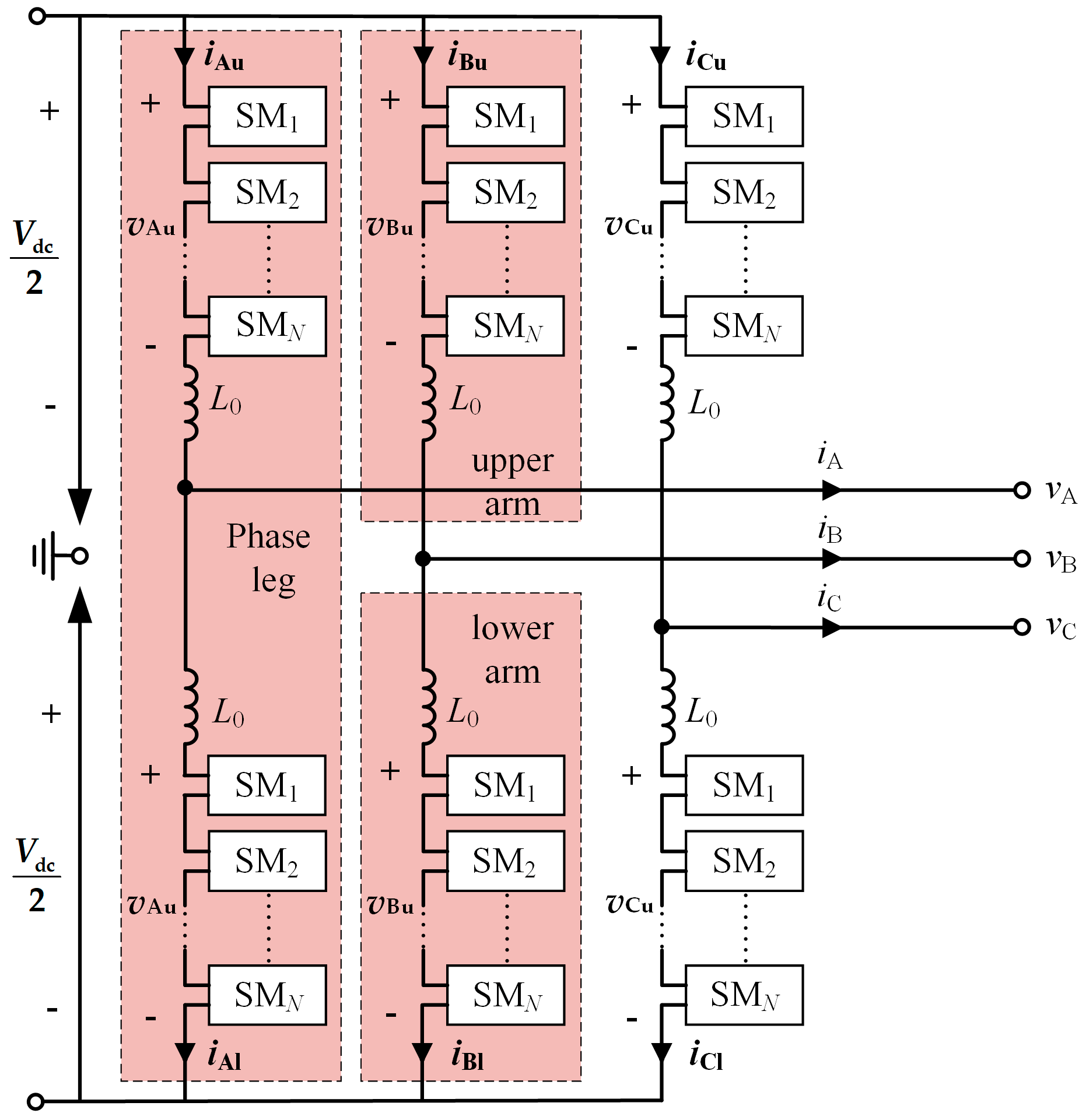
The topology of the modular multilevel converter (MMC) is shown in
Figure 1. The upper and lower arms of each phase are composed of
N half bridge sub-modules and an arm inductance
L0.
Vdc is the DC-link voltage,
vx (
x ∈ {A, B, C}) is the output-phase voltage,
ix is the output current.
vxu and
vxl are the voltage of the upper and lower arm, respectively.
ixu and
ixl are current of the upper and lower arm, respectively.
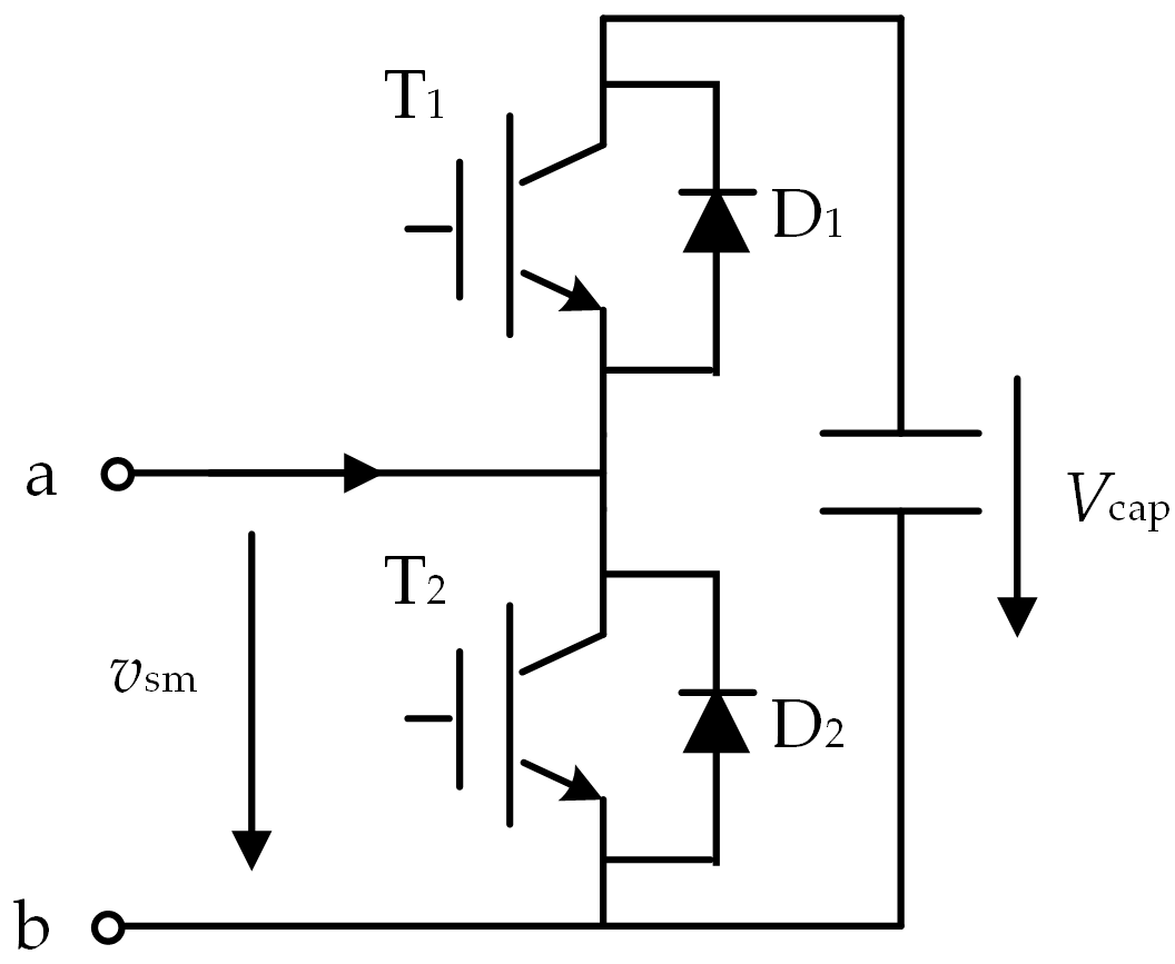
As the most basic component of the MMC, the sub-modules have been derived from various types of structures. This paper is an example of a half bridge sub-module (HBSM), as shown in
Figure 2. The sub-module topology is constructed from two IGBT power switching devices, T
1 and T
2, with anti-parallel diodes and an energy storage capacitor. The MMC controls the turn-on and turn-off states of each half bridge sub-module power switching device in the upper and lower arms to obtain the required output voltage on the AC side. Each anti-parallel diode ensures that the corresponding IGBT power switching device can be protected from the current when it is turned off, thus ensuring that the MMC can operate normally. When T
1 is turned on and T
2 is turned off, the energy storage capacitor will be charged or discharged according to the direction of the arm current flowing through it, when the sub-module is in the input state. When T
1 is off and T
2 is on, the output voltage of the sub-module is 0 V, and the arm current will not flow through the energy storage capacitor, at which time the sub-module is in the removal state. In addition, when both T
1 and T
2 are switched off, the sub-module will be in the removal state. When the arm current is positive, the capacitor is charged using the anti-parallel diode D
1; when the arm current is negative, the arm current will flow through the anti-parallel diode D
2, and the capacitor will be bypassed.
Table 1 shows the output voltage and switch state corresponding to the power switching device and defines the current direction of the arm current from end a to end b as the positive direction,
vsm is expressed as the output voltage of the sub-module unit and
vcap is the capacitance voltage of the sub-module.
The MMC equivalent mathematical model can reflect its operation principle visually, which is very important for the study of its operation control strategy. Firstly, in order to describe the equivalent mathematical model of the half bridge sub-module,
Sxki can be defined as the switching function of the sub-module, as shown in Equation (1).
where,
Sxki is the switching function of the
ith half bridge sub-module of the
k-arm in the
xth phase (
k = u, l), and when
Sxki = 1, the corresponding half bridge sub-module is in the input state, and when
Sxki = 0, the corresponding half bridge sub-module is in the removal state.
Since each half bridge sub-module is controlled individually, so that all half bridge sub-modules in the upper and lower arms can be equated to an independent controlled voltage source respectively, the output voltages,
vxu and
vxl, of the upper and lower arms in the
xth phase unit can be expressed as:
where,
N is the total number of sub-modules of the arm, and
vsm_xui and
vsm_xni are the output voltages of the
ith half bridge sub-module of the upper and lower arms of the
x phase, respectively.
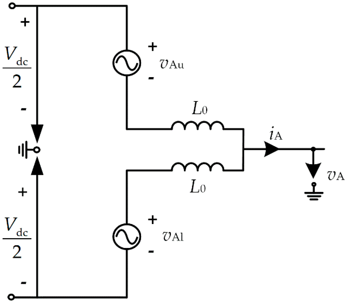
Because the three phase units of the MMC have the same structure and are controlled independently of each other, only a single phase needs to be analyzed. Taking phase A as an example, the single-phase equivalent circuit of the MMC is shown in
Figure 3.
The current flowing through the upper and lower arms is defined as the circulating current
icirA. According to Kirchhoff’s current law (KCL), the upper and lower arm currents can be expressed as:
According to (1), the circulating current is derived as:
The A-phase output voltage and output current are expressed as:
where,
VA is the RMS value of the output-phase voltage,
IA is the RMS value of the output current,
ω is the output fundamental angular frequency, and
φ is the power factor angle.
According to the single-phase equivalent circuit of the MMC, the voltage equation of the upper and lower arms can be obtained by Kirchhoff’s voltage law (KVL):
To facilitate the analysis of the MMC, the voltage modulation index of phase A is defined as the ratio of the amplitude of the output AC-phase voltage to half the DC-side voltage:
where,
is the amplitude of the output AC-phase voltage of phase A.
Ignoring the voltage drop in the arm inductance, the upper and lower arm voltage can be further expressed as:
Substituting (3) with (7), it can be obtained that:
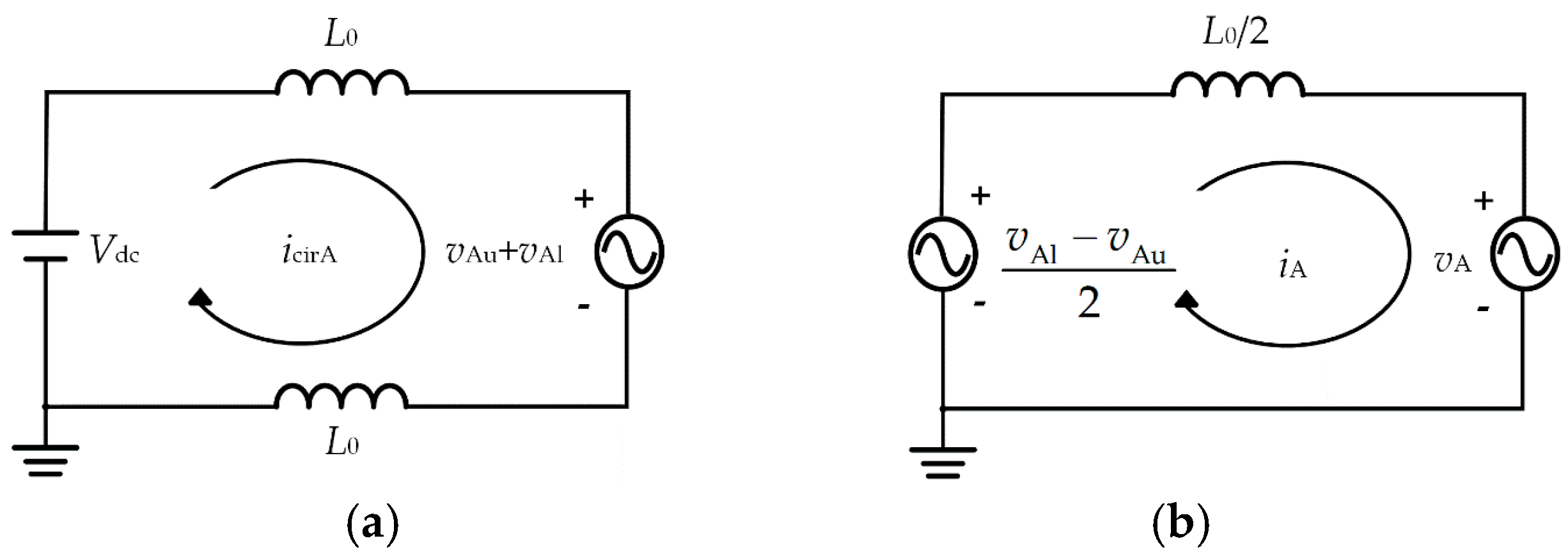
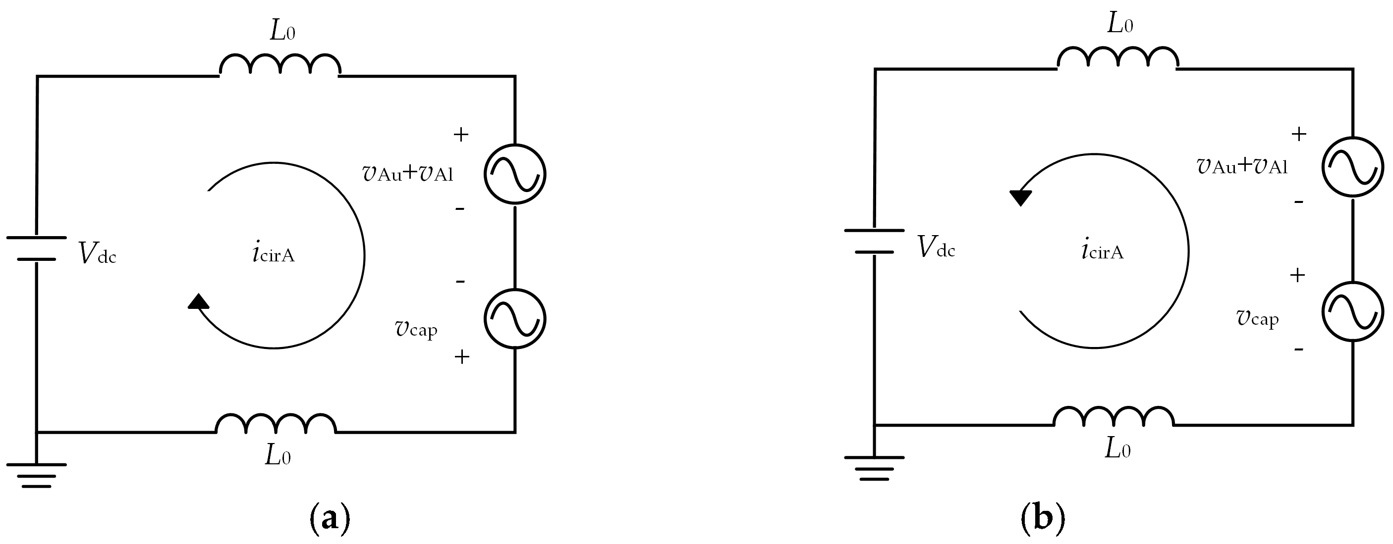
In order to more directly describe the energy exchange process inside the MMC and the relationship between each electrical quantity, the equivalent circuit of phase A can be decomposed into the DC-side equivalent circuit and the AC-side equivalent circuit, as shown in
Figure 4a,b.
Figure 4a depicts the energy exchange process between the MMC and the DC side, which reflects the correlation between each electrical quantity within the topology, so that the MMC can indirectly control the circulating current to achieve a specific goal using Equation (10). Equation (11) and
Figure 4b both describe the process of energy interaction between the MMC and the AC side, which reflects that the MMC can get the required output voltage on the AC side by controlling the opening and closing states of each half bridge sub-module power switching device in the upper and lower arms.
3. Improved 2N+1 Pulse-Width Modulation Approach
The control strategy can rely on the pulse-width modulation approach to generate pulses to control the MMC and, thus, improve the system performance. The carrier-based pulse-width modulation approach is often used in the MMC because of its simplicity, scalability and good control performance. Compared with other converters, the MMC can generate two different types of output-phase voltage levels,
N+1 and 2
N+1, depending on the different arrangements of the multiple carrier signals in the upper and lower arms and the parity of the number of sub-modules in the arm.
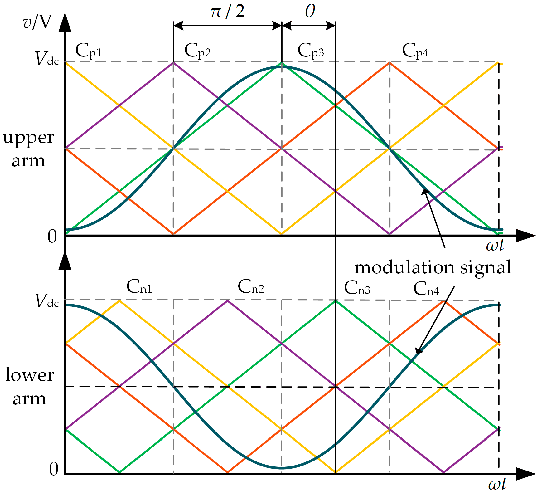
Figure 5 shows the principle of the conventional carrier phase-shifted 2
N+1 pulse-width modulation approach under the
N = 4 condition. Each arm requires a modulation signal and a set of four carrier signals with the frequency of
fc and the phase difference of π/2. At the same time, since the upper and lower arms in the MMC phase cell operate symmetrically, the phases of the modulated signals of the upper and lower arms need to differ from each other by π. The carrier signals of the upper arm are defined as C
p1~C
p4, and the carrier signals of the lower arm are defined as C
n1~C
n4. Taking C
p1 and C
n1 as an example, the phase shifting angle
θ between the carrier signals of the upper and lower arm is π/4.
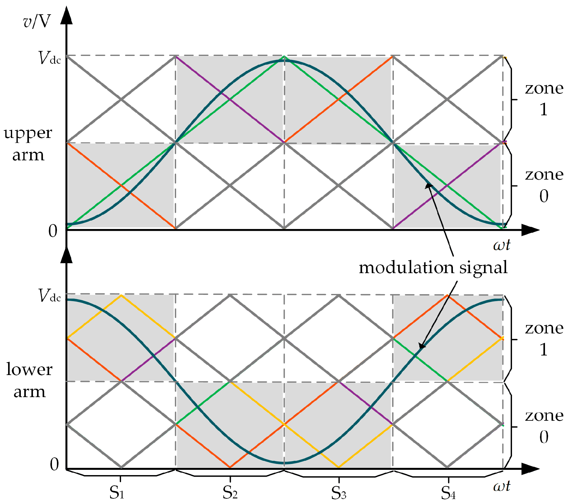
With the increase in sub-modules in each arm, the number of carrier signals is increased correspondingly. Moreover, the accurate synchronization of the different carrier signals will be more difficult. In order to solve the above problem, an improved 2
N+1 pulse-width modulation approach is proposed. Only two carrier signals are used to generate 2
N+1 level output-phase voltage. Taking
N = 4 as an example, the principle of the improved 2
N+1 pulse-width modulation approach is shown in
Figure 6. The fundamental period is divided into four segments, and the carrier wave is divided into two zones, according to its amplitude. There are only two carrier signals with a phase difference of π in any arbitrary rectangle determined by the segment number and zone number.
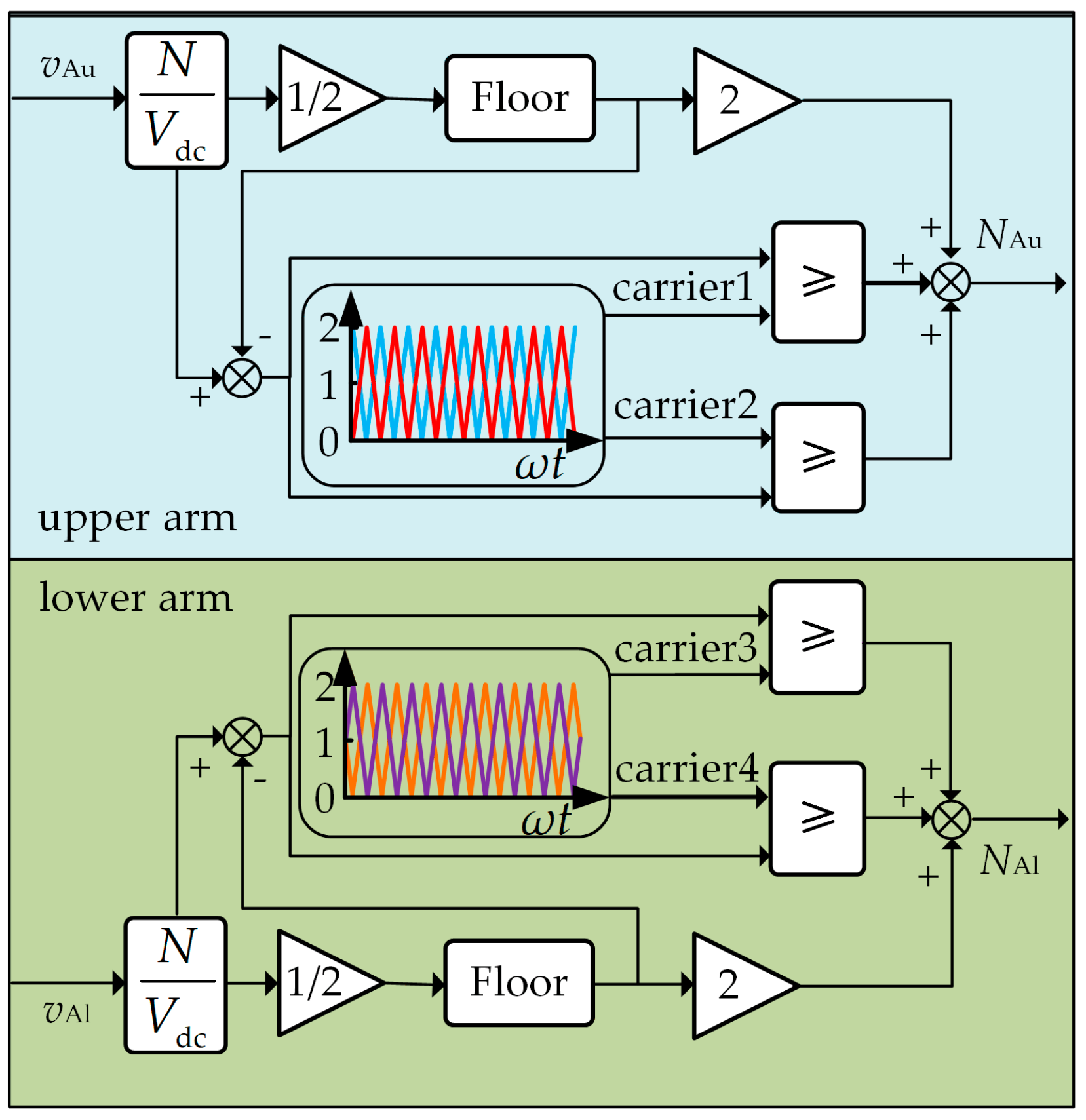
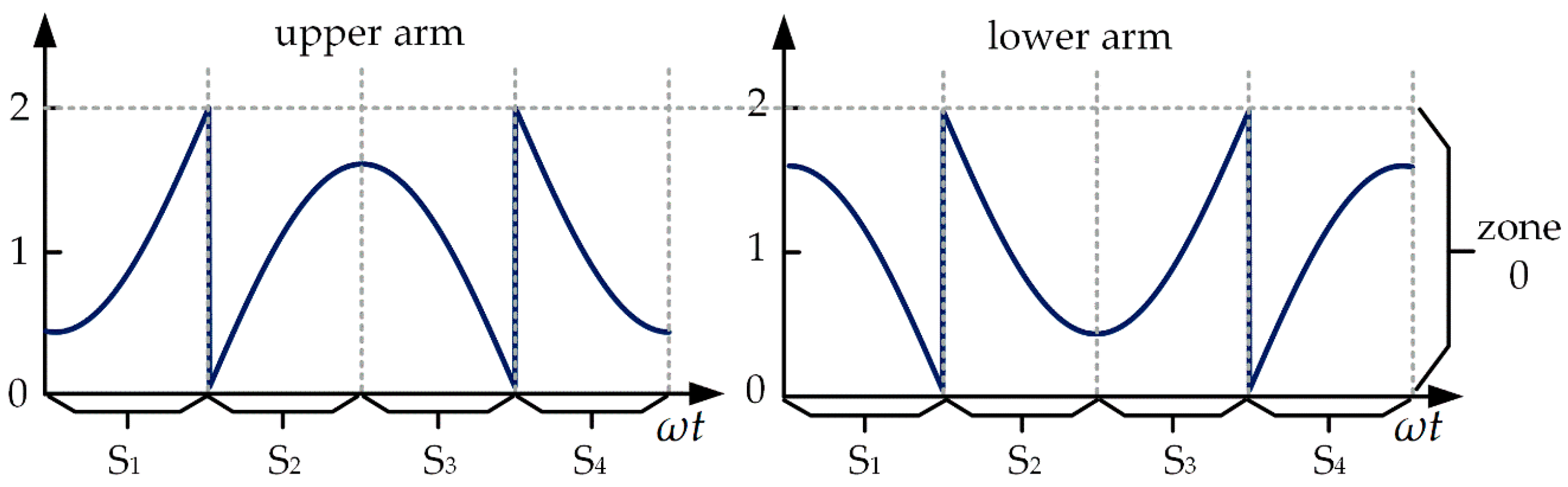
Figure 7 shows the block diagram of the improved modulation method. The implementation of the proposed method can be divided into three steps: the generation of the segment and zone number, the integration of the modulation signal, and the comparison of the modulation signal and the carrier signal. In each segment, the modulation signal is vertically shifted to zone 0, to generate an integrated modulation signal, as shown in
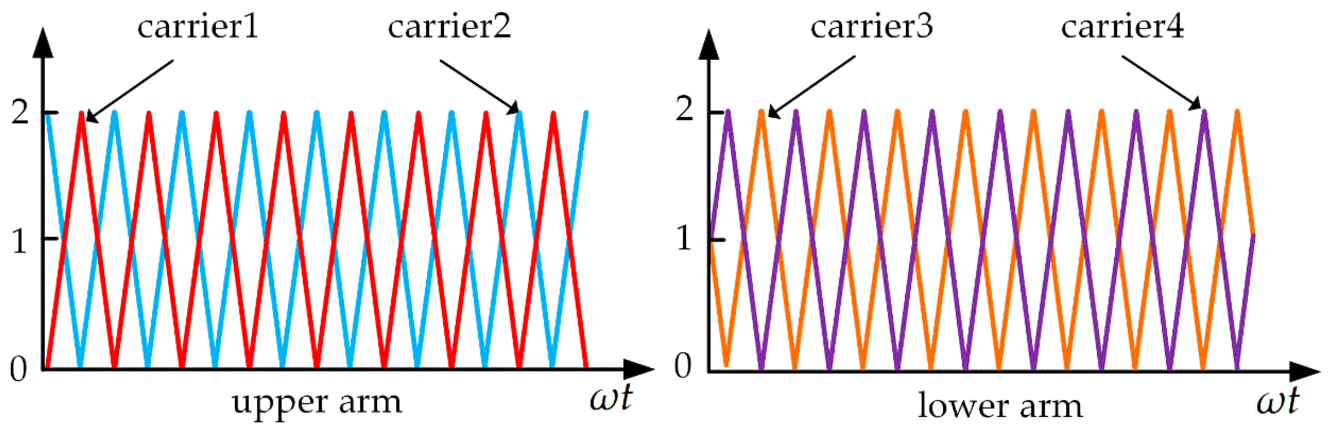
Figure 8. Only two carrier signals with a phase difference of π are adopted in each arm, as shown in
Figure 9. The carrier signal of the lower arm is shifted by π/2 with respect to the upper arm (the phase difference between carrier 1 and carrier 2 is π, the phase difference between carrier 1 and carrier 3 is π/2, and the phase difference between carrier 2 and carrier 4 is also π/2). The carrier signals set on the upper and lower arms are compared with the corresponding modulated wave integration signals, respectively. The carrier signals are compared with the corresponding integrated modulation signals of the upper and lower arms, respectively. Finally, the comparison results are superposed with the segment and zone number to generate the number of sub-modules needed to be switched in for the upper and lower arms. Then, the driving pulse of each sub-module is generated.
4. Circulating Current Suppression Strategy
For the three-phase MMC with
N sub-modules in each arm, the phase voltage will appear at the
N+1 voltage level if the total number of switched-in sub-modules in each phase remains
N. If the total number of switched-in sub-modules changes among
N−1,
N, and
N+1, the phase voltage will appear at the 2
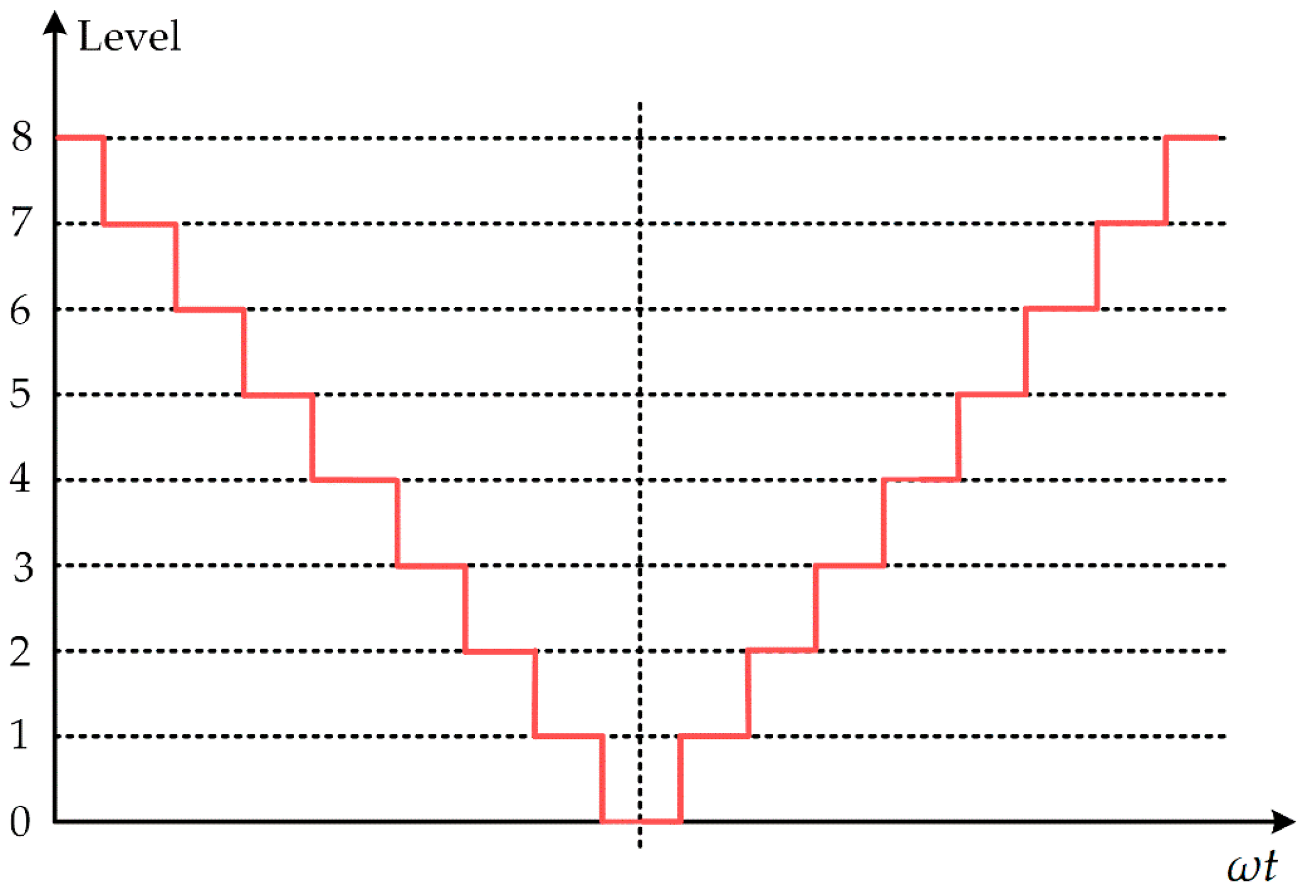
N+1 voltage level. Taking
N = 4 as an example, the output-phase voltage of the 2
N+1 modulation method is shown in
Figure 10. The relationship between the total number of switched-in sub-modules and the output-phase voltage level is shown in
Table 2. It follows that the switching states generated by its 2
N+1 modulation strategy consist of non-redundant switching states and redundant switching states. When the number of phase voltage levels on the output side of the MMC system is 0, 2, 4, 6, or 8 even levels, only one switch state type can generate that phase voltage level and a total of four sub-modules are put into the phase arm. When the number of phase voltage levels on the output side of the MMC system is 1, 3, 5, or 7 odd levels, there are two switching state types to generate that phase voltage level and a total of three or four sub-modules are put into the phase arm. Therefore, for the even output voltage level,
N sub-modules are switched in for each phase. While for the odd output voltage level, the
N+1 or
N−1 sub-modules are switched in for each phase. Thus, there is only one switching state corresponding to even output voltage level and there are two switching states corresponding to the odd output voltage level. The DC-side equivalent circuit of the MMC is shown in
Figure 11. The circulating current will increase if the
N−1 sub-modules are switched in. The circulating current will decrease if the
N+1 sub-modules are switched in. Thus, the circulating current can be controlled by the above two switching states.
The instantaneous power of the upper and lower arms can be expressed as:
For MMC, the circulating current only contains even order harmonic components. Moreover, the second order harmonic component accounts for a large proportion [
24]. The circulating current can also be expressed as:
where
IcirA_dc is the DC component of the circulating current, and
IcirA_2 and
θ are the RMS value and the phase of the second order harmonic component of the circulating current, respectively.
In order to suppress the circulating current, the reference value of the circulating current can be set to the value of the DC component. Meanwhile, to ensure the power balance between the DC side and the AC side of the MMC, the DC component of the instantaneous power of the arm should be kept at zero [
25]. Therefore, the reference value
of the circulating current can be derived as:
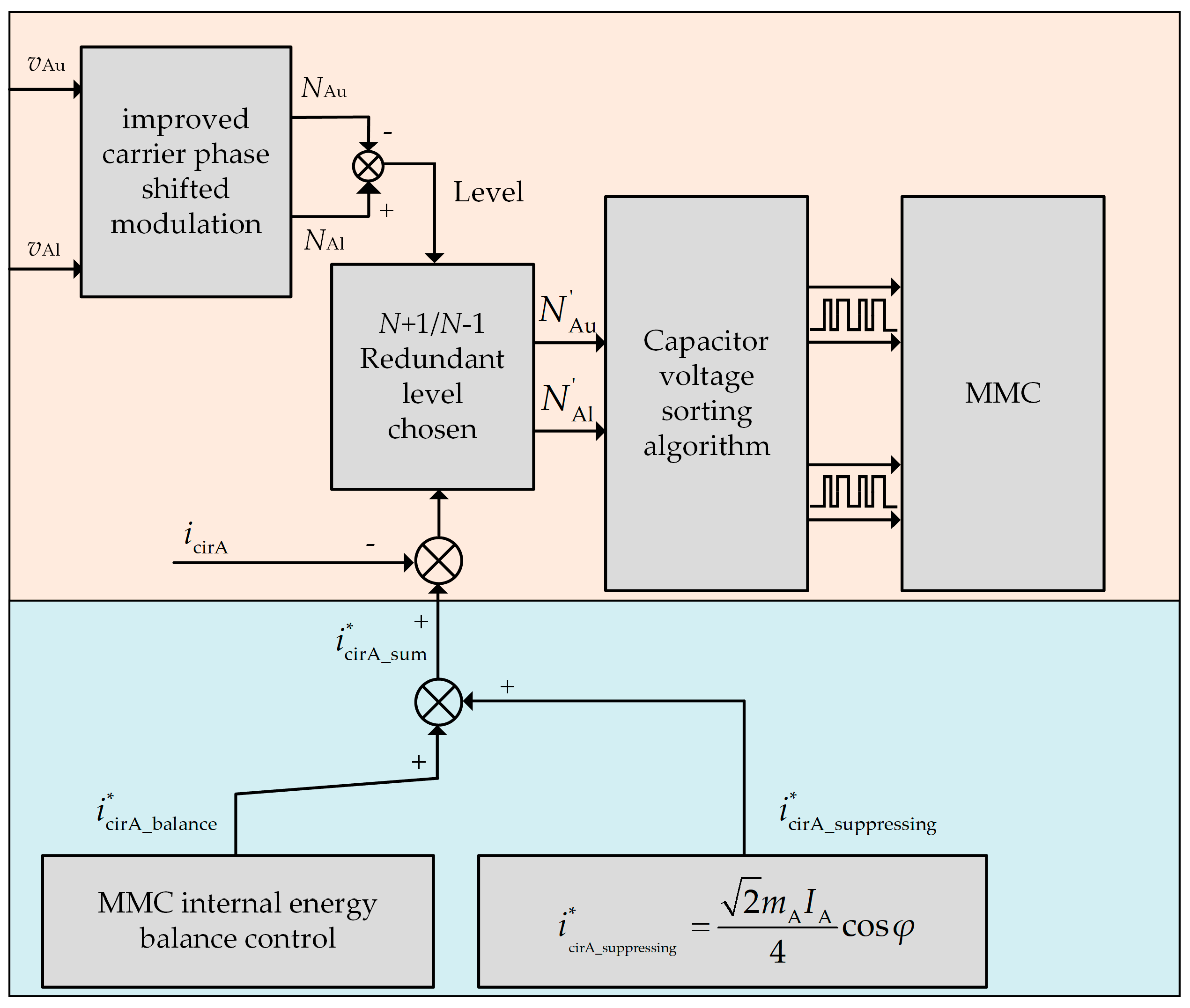
Taking the A-phase as an example, the block diagram of the circulating current suppression strategy based on the improved 2
N+1 pulse-width modulation approach is shown in
Figure 12. Based on the modulation signals of the upper and lower arms, the number of sub-modules that need to be switched in is determined by the improved carrier phase-shifted 2
N+1 modulation method. The circulating current can be adjusted to its reference value
by the redundant switching state (
N+1 or
N−1 sub-modules are switched in).
consists of a reference component
generated by the MMC internal energy balance control [
26] and a reference component
aimed at suppressing the circulating current. That is, when the voltage level is at the redundant level and
icirA ≤
, the
N−1 sub-modules are selected to be put into the phase, so that the circulating current inside the topology rises; conversely, when the voltage level is at the redundant voltage level and
icirA >
, the
N+1 sub-modules are selected to be put into the phase, so that the circulating current inside the topology falls and, finally, after the capacitor voltage sequencing algorithm, the trigger pulse is applied to the modular multilevel converter. In particular, the capacitor voltage sorting algorithm [
27] in this block diagram, the most widely used method for balancing the capacitive voltage of sub-modules, determines the specific sub-modules to be put into the bridge arm by sorting the capacitive voltage of all sub-modules in the arm and determining the number of sub-modules to be put into the arm at the present time, as well as the direction of the arm current. The purpose of this is that when the arm current is positive, the sub-module with the lower capacitor voltage is engaged for a longer period of time to charge the capacitor, while when the arm current is negative, the sub-module with the higher capacitor voltage is engaged for a longer period of time to discharge the capacitor.
5. Experimental Verification
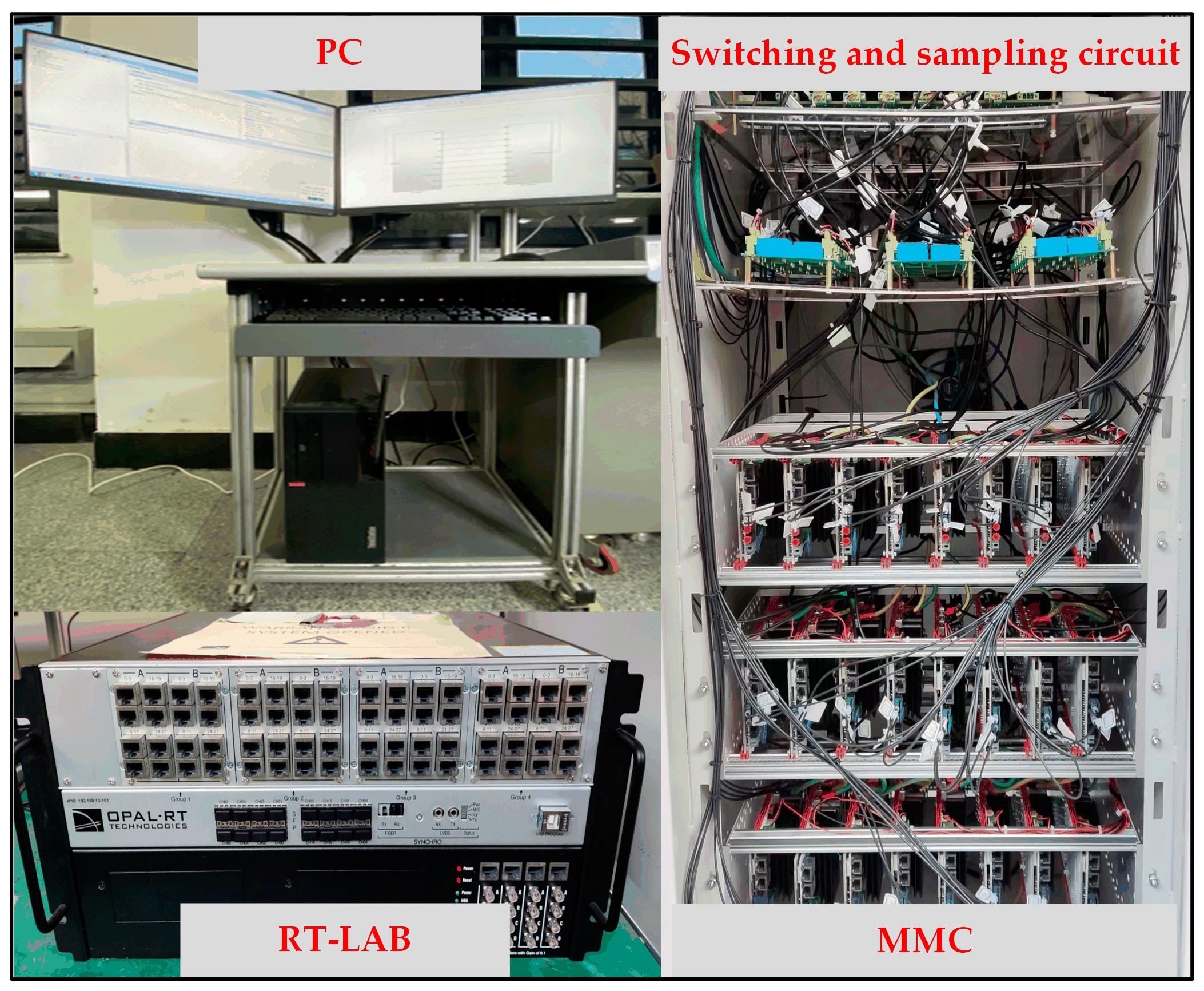
To verify the performance of the circulating current suppression strategy of the MMC based on the improved 2
N+1 pulse-width modulation approach, the simulation models of the three-phase MMC system were developed in MATLAB/Simulink. In addition, the experimental prototype of the three-phase MMC system was designed and developed in the laboratory. The Canadian Opal-RT
® rapid prototyping system OP5700 was adopted as the controller and the Switzerland Imperix
® PEH2015 power electronic building block was used to compose the MMC (
N = 4), as shown in
Figure 13. The load condition was set as a simple resistor–inductor (R–L) (resistor–inductor) load. Based on the instantaneous power of the upper and lower arms, it is known that the control performance of the MMC depends on the power factor and, therefore, the simulations and experiments with the proposed 2
N+1 pulse-width modulation method and the conventional carrier phase-shifted 2
N+1 pulse-width modulation method are carried out under different load power factor conditions. The parameters for the simulations and experiments are shown in
Table 3.
To demonstrate the simplicity of the implementation of the proposed 2
N+1 pulse-width modulation method, the MMC simulations were developed using the parameters for simulation in
Table 3. When the arm is used with eight sub-modules, the proposed method requires only two differently phased carriers compared to the conventional carrier phase-shifted modulation method, which requires eight differently phased carriers, thus the control complexity of the system is reduced.
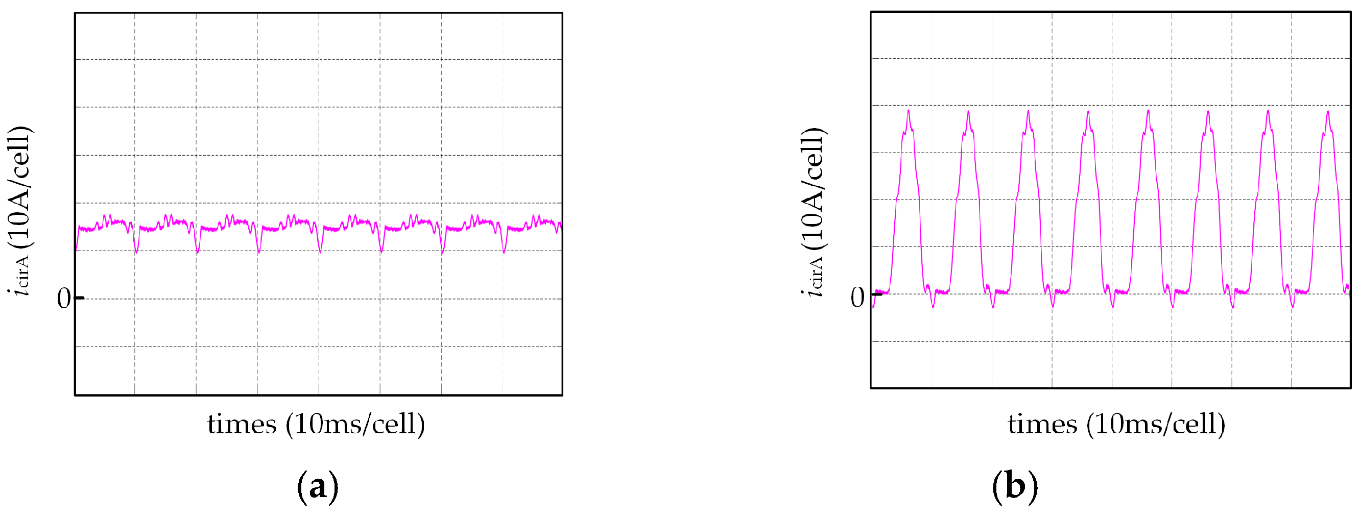
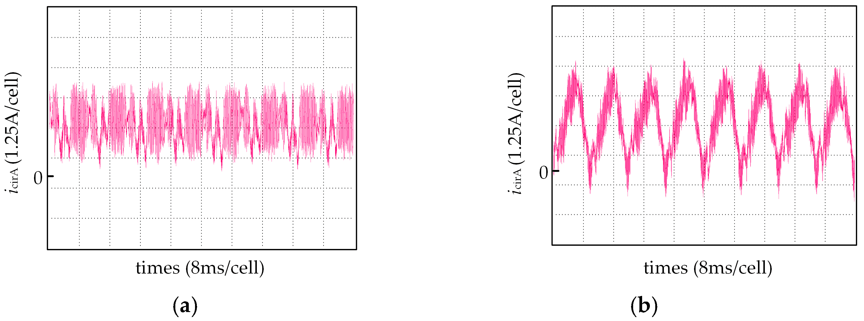
The circulating current,
icirA, of the proposed method and the conventional method under different load power factor conditions are shown in
Figure 14 and
Figure 15. For cos
φ = 0.954, the simulated ripples of the circulating current are 8.1 A and 41 A for the proposed method and the conventional method, respectively. For cos
φ = 0.623, the simulated ripples of the circulating current are 6.2 A and 16.5 A for the proposed method and the conventional method, respectively. It is clear that the proposed method can suppress the circulating current effectively.
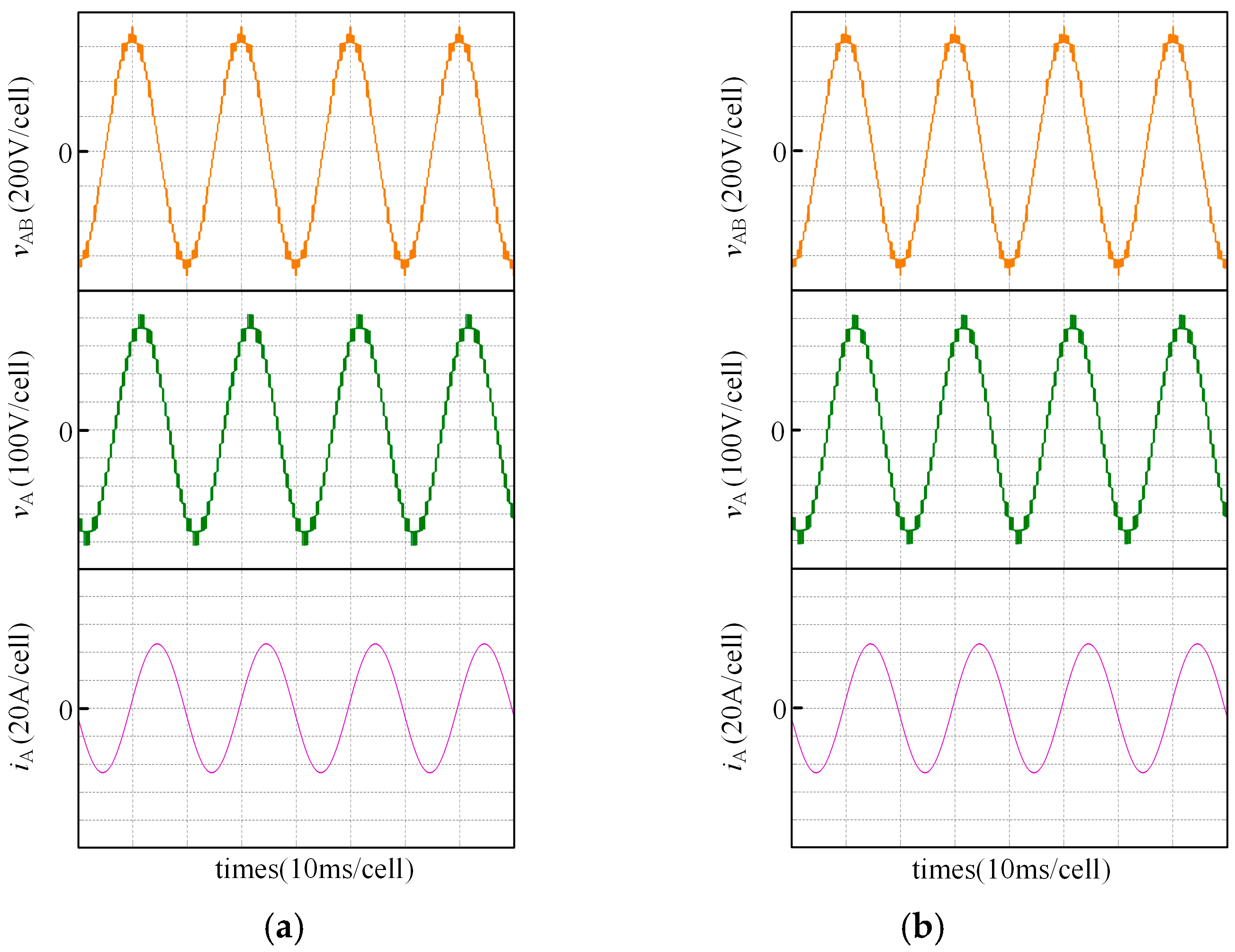
The output line voltage
vAB, the output-phase voltage
vA, and the output current
iA of the proposed method and the conventional method under different load power factor conditions are shown in
Figure 16 and
Figure 17. As the arm contains eight sub-modules, the number of levels in the output-phase voltage waveform under the 2
N+1 modulation is 17 levels for
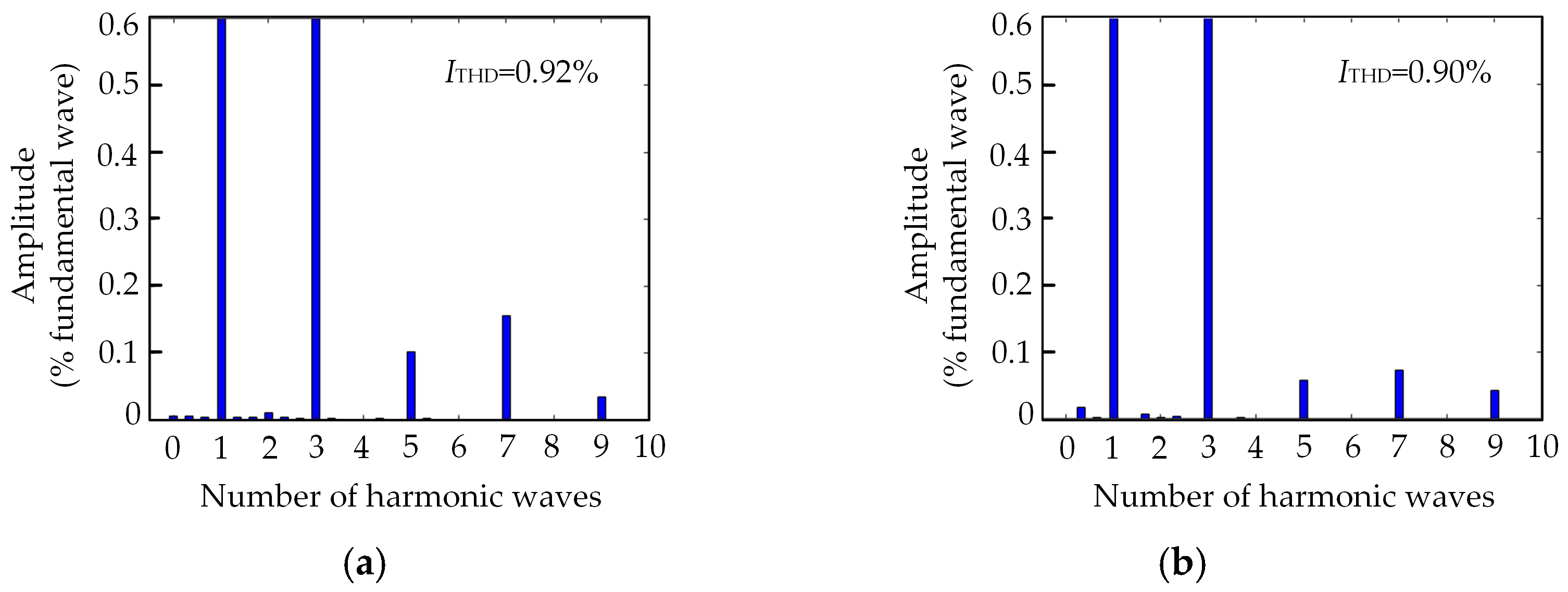
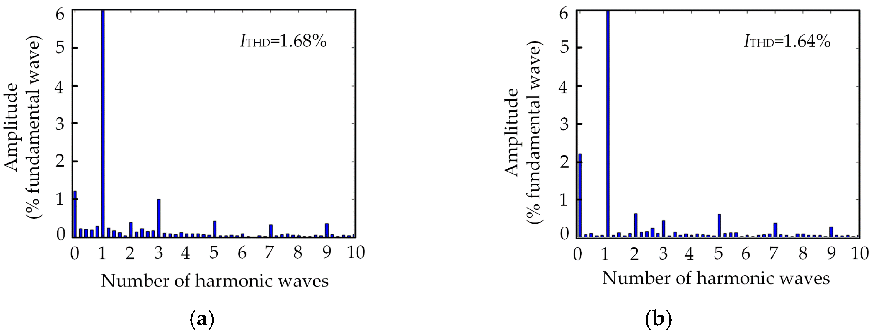
m = 0.9. If the total harmonic distortion rate of the output current is used as the evaluation standard for the MMC output waveform, the total harmonic distortion of the output current
ITHD for the proposed method and the conventional method under different load power factor conditions are shown in
Figure 18 and
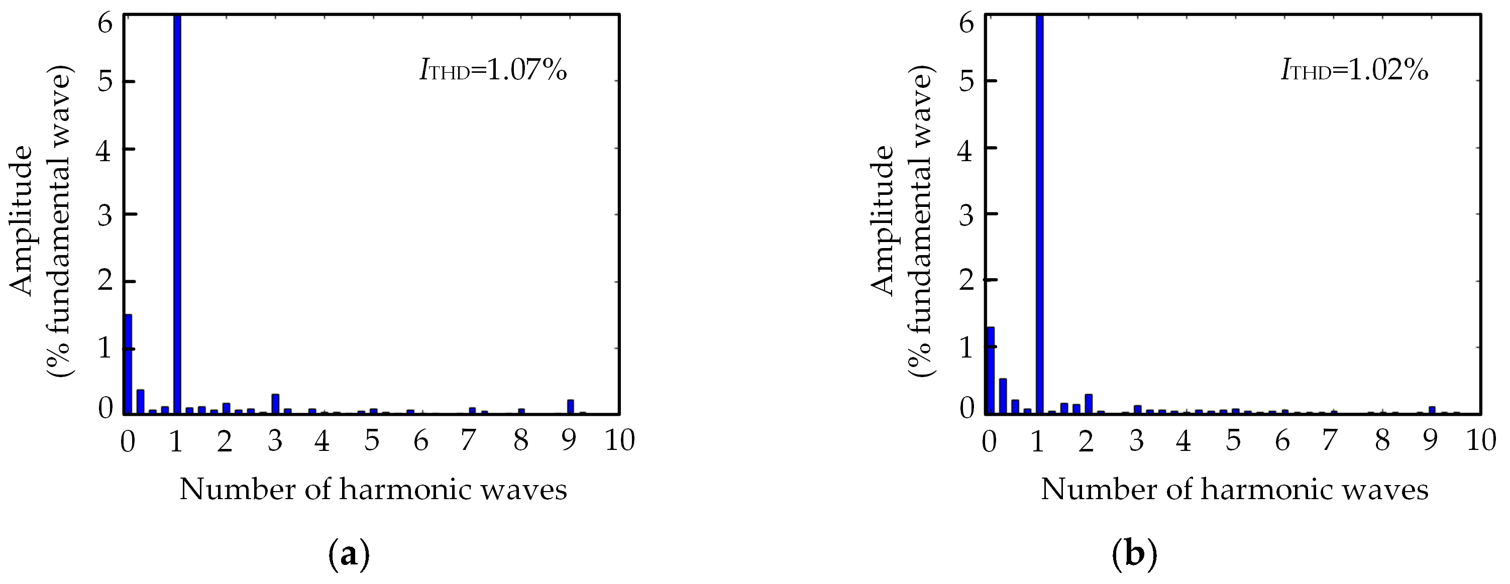
Figure 19. The
ITHD of the proposed and the conventional methods are approximately the same. This demonstrates the similarity in the output performance between the proposed modulation method and the conventional modulation method.
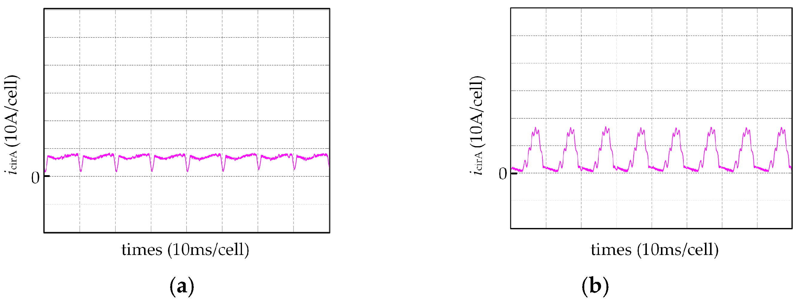
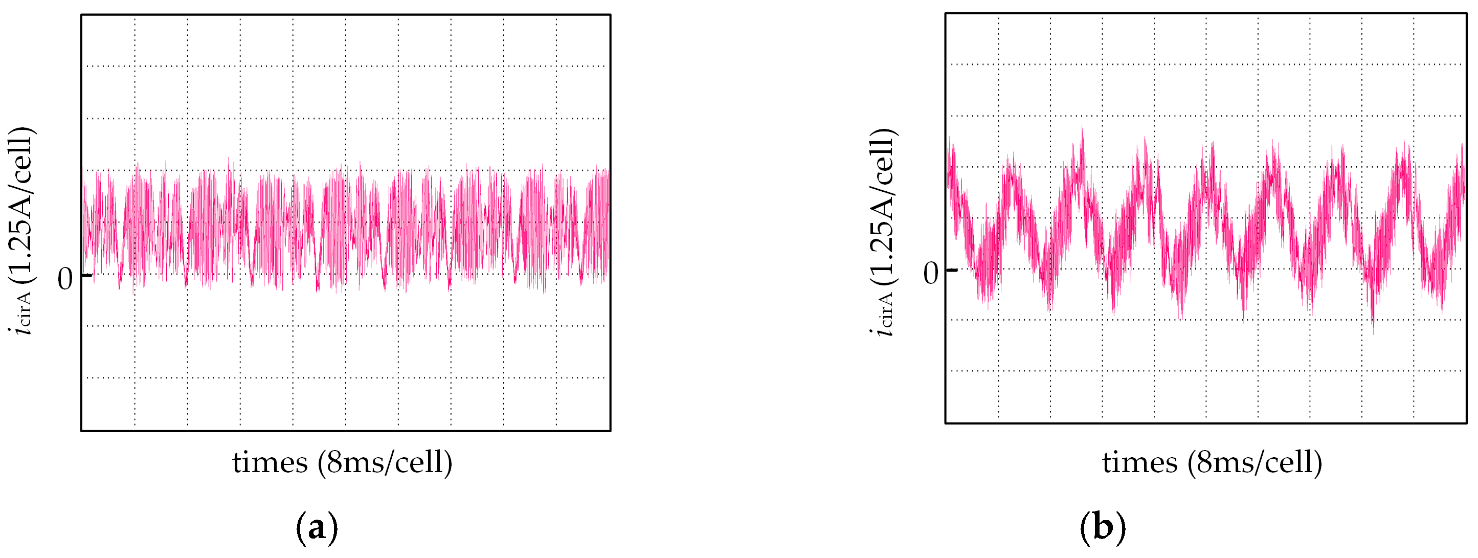
Furthermore, the proposed method was verified through the experimental prototype of the three-phase MMC system. The circulating current
icirA of the proposed method and the conventional method under different load power factor conditions are shown in
Figure 20 and
Figure 21. For cos
φ = 0.954, the ripples of the circulating current are 3.8 A and 5.8 A for the proposed method and the conventional method, respectively. For cos
φ = 0.623, the ripples of the circulating current are 3.4 A and 4.4 A for the proposed method and the conventional method, respectively. It is obvious that the proposed method uses redundant switching states with the 2
N+1 modulation to regulate the circulating current of the MMC with its reference value in order to achieve the effect of suppressing the circulating current fluctuations at different load power factors.
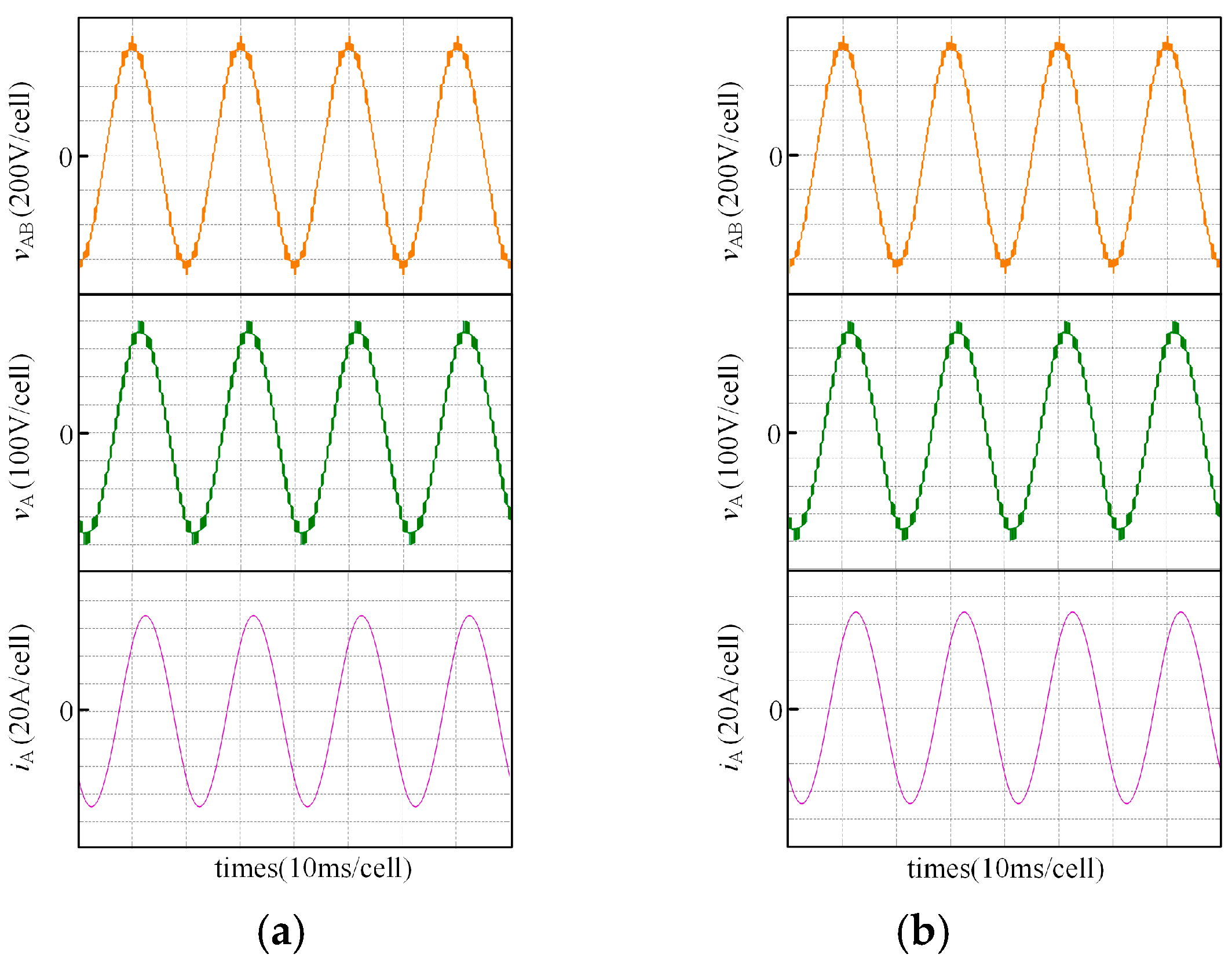
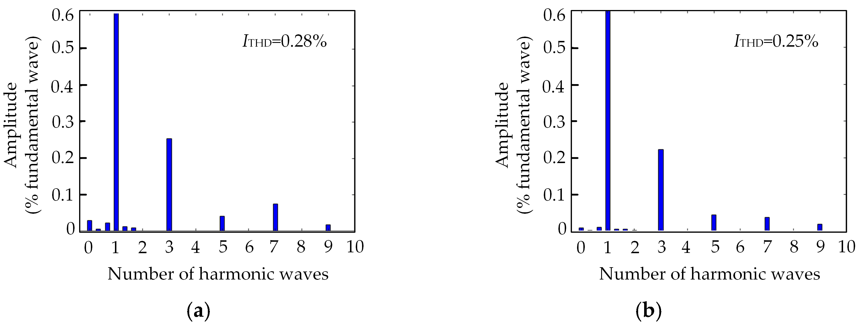
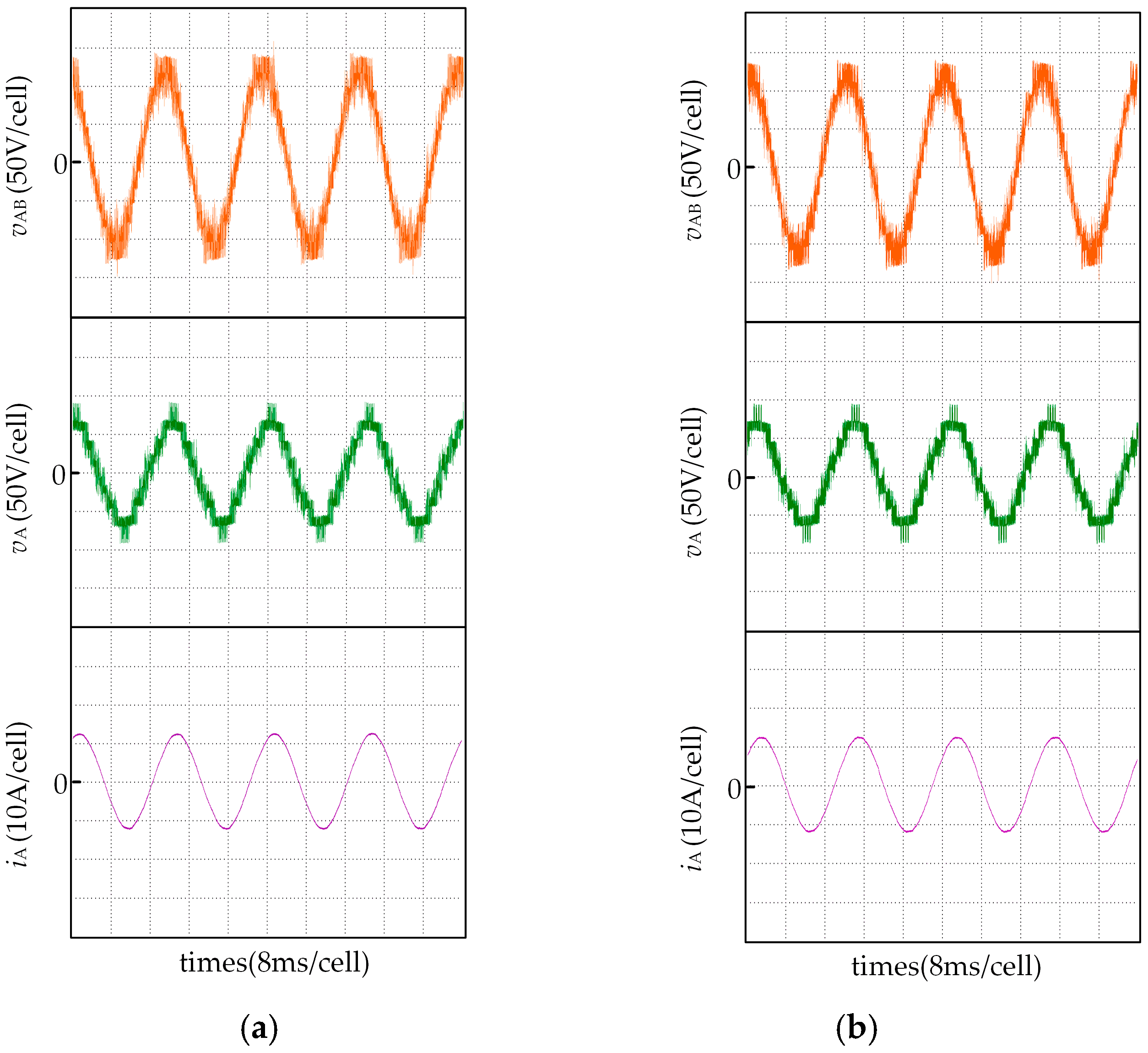
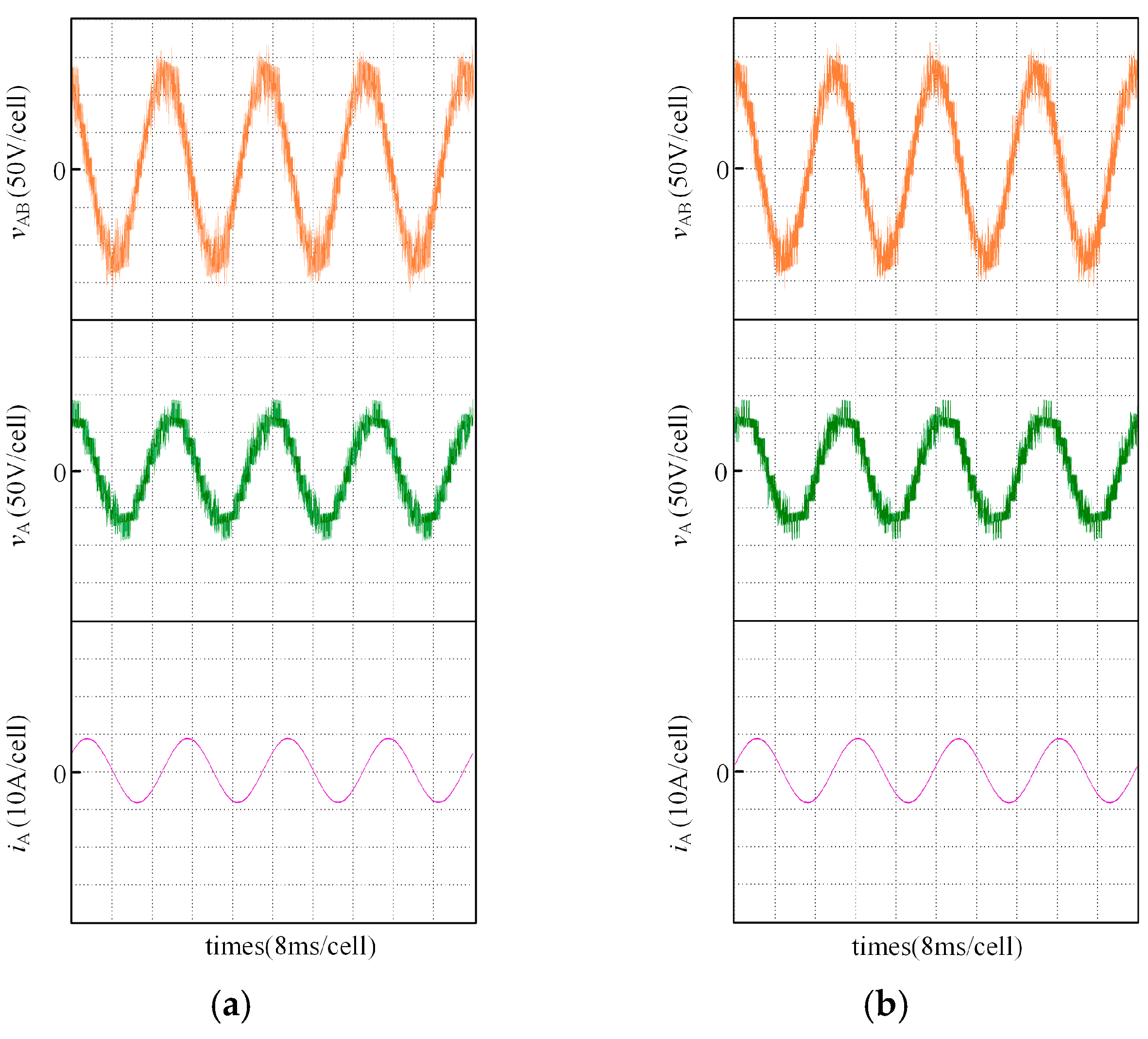
To demonstrate the similarity between the proposed modulation method and the conventional modulation method, the experimental output waveforms of the two methods for different power factor conditions are shown in
Figure 22 and
Figure 23. As can be seen, for
m = 0.8, the output-phase voltage of the carrier phase-shifted 2
N+1 modulation method has nine voltage levels. Thus, the output current is an undistorted sinusoidal waveform. For different load power factors, the
ITHD of the proposed and the conventional methods are approximately the same, as shown in
Figure 24 and
Figure 25. This proves that the proposed modulation method presents an identical performance to the conventional modulation method. Thus, the proposed method not only reduces the circulating current, but also ensures the quality of the output waveform, the advantages of which are shown in
Table 4 and
Table 5.


