Article

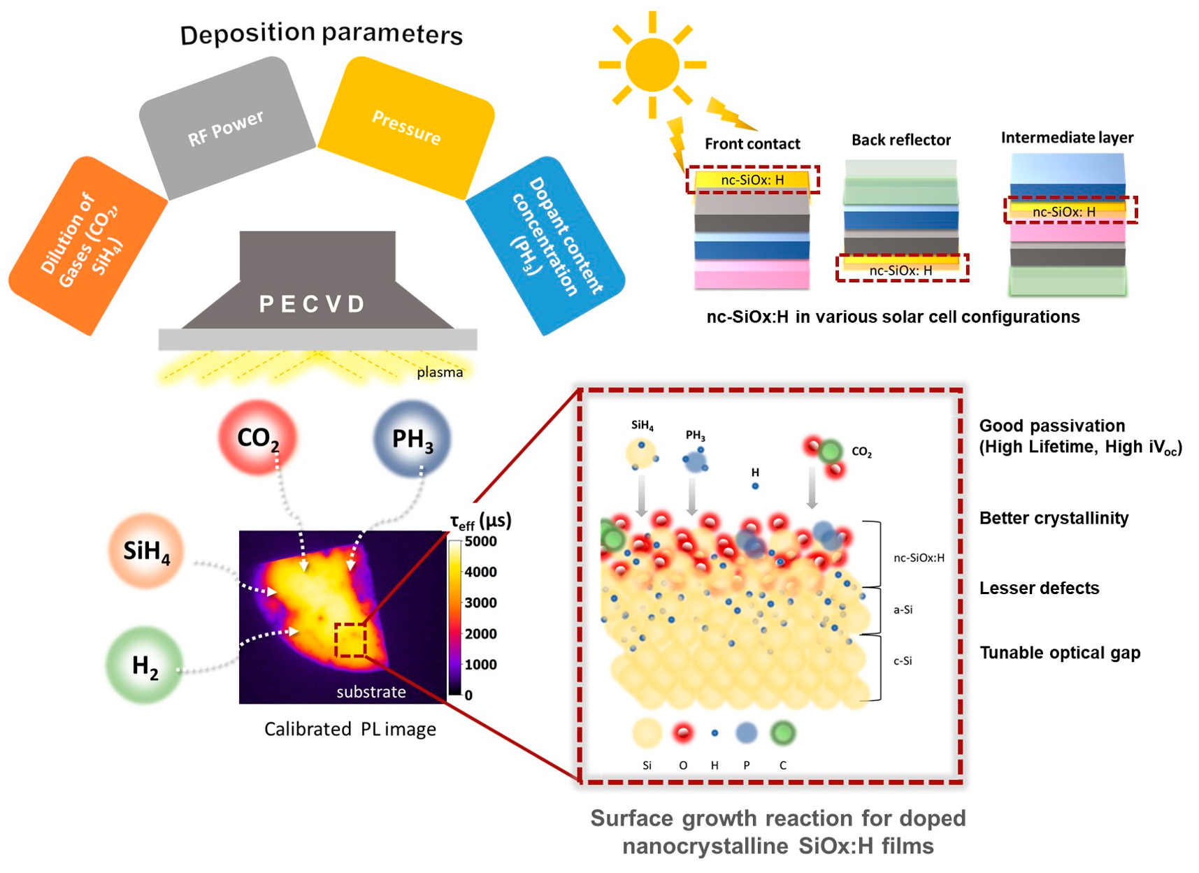
Development of n-Type, Passivating Nanocrystalline Silicon Oxide Films via Plasma-Enhanced Chemical Vapor Deposition

by
Gurleen Kaur
1,2,*,
Antonio J. Olivares
2 and
Pere Roca i Cabarrocas
1,2,*
1
Institut Photovoltaïque d’Ile-de-France (IPVF), 18 Bvd Thomas Gobert, 91120 Palaiseau, France
2
Laboratoire de Physique des Interfaces et Couches Minces (LPICM), Ecole Polytechnique, Institut Polytechnique de Paris, Route de Saclay, 91128 Palaiseau, France
*
Authors to whom correspondence should be addressed.
Solar 2024, 4(1), 162-178; https://doi.org/10.3390/solar4010007
Submission received: 15 January 2024 / Revised: 2 March 2024 / Accepted: 5 March 2024 / Published: 11 March 2024
(This article belongs to the Special Issue Developments in Perovskite Solar Cells)

Abstract

:
Nanocrystalline silicon oxide (nc-SiOx:H) is a multipurpose material with varied applications in solar cells as a transparent front contact, intermediate reflector, back reflector layer, and even tunnel layer for passivating contacts, owing to the easy tailoring of its optical properties. In this work, we systematically investigate the influence of the gas mixture (SiH4, CO2, PH3, and H2), RF power, and process pressure on the optical, structural, and passivation properties of thin n-type nc-SiOx:H films prepared in an industrial, high-throughput, plasma-enhanced chemical vapor deposition (PECVD) reactor. We provide a detailed description of the n-type nc-SiOx:H material development using various structural and optical characterization techniques (scanning electron microscopy (SEM), energy dispersive X-ray (EDX), Raman spectroscopy, and spectroscopic ellipsometry) with a focus on the relationship between the material properties and the passivation they provide to n-type c-Si wafers characterized by their effective carrier lifetime (τeff). Furthermore, we also outline the parameters to be kept in mind while developing different n-type nc-SiOx:H layers for different solar cell applications. We report a tunable optical gap (1.8–2.3 eV) for our n-type nc-SiOx:H films as well as excellent passivation properties with a τeff of up to 4.1 ms (implied open-circuit voltage (iVoc)~715 mV) before annealing. Oxygen content plays an important role in determining the crystallinity and hence passivation quality of the deposited nanocrystalline silicon oxide films.

Graphical Abstract

1. Introduction

In the past decade, nanocrystalline silicon oxide (nc-SiOx:H) films, as a functional multipurpose material, have garnered significant interest of the photovoltaic community [1,2,3,4]. This is due to its broad range of optical and electrical properties, which can be tuned by varying deposition parameters: i.e., absorption coefficient, refractive index, optical band gap, and p-type and n-type doping, which allow it to make selective contacts. Doping films with phosphorus (n-type) has resulted in further improved conductivities, and hydrogen atoms in the mixture have resulted in effective defect passivation [5]. Nanocrystalline silicon oxide (nc-SiOx:H) consists of crystalline silicon nanoparticles embedded in an amorphous phase composed of silicon oxide (a-SiOx:H) and a-Si:H phases [6,7]. The two-phase structure of nc-SiOx:H materials has been suggested to help achieve a large optical gap while keeping a high conductivity. The oxygen-rich Si-O-Si phase of the material helps to increase the optical gap and decrease the refractive index, while the Si-rich portion of the material, via an intricate three-dimensional network of crystallites, is known to provide high electrical conductivity pathways both in lateral and transverse directions [8].
The research on nc-SiOx:H layers was first developed for single-junction μc-Si:H solar cells. It provided better light trapping and acted as a good window layer [4,9,10,11]. By using a suitable bilayer of two crystalline SiOx:H layers (as n-layer as well as back reflector), solar cell efficiencies improved in p-i-n structure-based single-junction solar cells [12]. Later on, the material was applied to silicon heterojunction (HJT) solar cells on both textured and flat substrates, where the nanocrystalline silicon oxide layer (nc-SiOx:H) has been used as a wide-gap window layer instead of an a-Si:H layer [13,14]. Compared with a-Si:H layers, n-type nc-SiOx:H offers higher transparency, similar electrical conductivity, and a lower refractive index. Mazzarella et al. also studied the use of ~5 nm thick n-type nc-SiOx:H as front contacts (exhibiting high front surface field) in rear-emitter SHJ solar cells, resulting in efficiencies of 22.6% [15]. The use of nc-SiOx as an electron transport layer has subsequently improved the power conversion efficiency to 23.1% (Voc = 738 mV, Jsc to 39 mA cm−2) [16].
Doped nc-SiOx:H layers also have dual application in tandem thin films solar cells: (i) as an intermediate reflector between the n/p recombination junction (i.e., a-Si:H and μc-Si:H) due to better refractive index matching and (ii) as an n-layer of the μc-Si:H bottom cell to reduce parasitic absorption [6,10,17]. The application of n-type and p-type nc-SiOx:H as an FSF layer and rear-emitter layer resulted in a textured rear-emitter SHJ solar cell with an efficiency of 21.4% [8]. Even poly-Si layers in TOPCon solar cells have been replaced by ultrathin nc-SiOx:H to enhance transparency [18,19]. Further, nc-SiOx layers have demonstrated clear advantages for maximizing the infrared response of c-Si bottom cells in combination with perovskite top cells [20]. Nanocrystalline silicon oxide (nc-SiOx:H) layers, in this case, not only offer better carrier transport and field effect passivation but also improve carrier selectivity and reduce parasitic absorption [21]. Depending on the application, these layers fulfil various requirements, such as (i) a doped layer to create the electric field in the diode, (ii) a nucleation layer to promote crystalline growth, or (iii) a suitable recombination junction with low series resistance. Therefore, in this work, we discuss the versatility of nanocrystalline silicon oxide (nc-SiOx:H) material deposited by an industrial, high-throughput plasma-enhanced chemical vapor deposition (PECVD) tool for different photovoltaic applications: front contacts, back reflectors, and intermediate window layers. Parameters like concentration of dilution gases, doping gases, RF power, and total pressure are examined in a detailed manner as illustrated in Figure 1a. During the PECVD deposition of nc-SiOx:H, silane (SiH4) provides silicon, carbon dioxide (CO2) supplies oxygen, phosphine (PH3) introduces phosphorus for doping, and hydrogen (H2) serves various functions such as influencing film properties and reducing defects. The combination of these precursor gases, along with the plasma environment, allows for the controlled growth of nc-SiOx:H with a tailored composition and properties for specific applications in solar cells.
Through this work, we explore and try to understand the relationship between the optical and structural properties of n-type nc-SiOx:H films and their ability to passivate the surface of crystalline silicon as systematically illustrated in Figure 1b. It should be noted that passivation quality of nc-SiOx:H films is a critical factor influencing the performance and efficiency of solar cells. For n-type c-Si wafers, passivation is particularly crucial as it helps to minimize the surface recombination of minority carriers, such as holes, and nc-SiOx:H films act as passivation layers for the silicon surface. The material properties, including the crystallinity, hydrogen content, and oxygen content, significantly influence the ability of these films to passivate the surface effectively. The presence of hydrogen is essential for passivation, as it helps in the formation of silicon–hydrogen bonds that can passivate dangling bonds and trap charge carriers. By understanding and controlling the deposition parameters, it is possible to tailor the passivation layer to suit the specific requirements of n-type c-Si wafers in solar cell applications. This paper distinguishes itself from previous studies by placing a pronounced emphasis on passivation properties within the realm of nanocrystalline silicon oxide (nc-SiOx:H) films. While prior research has predominantly examined these films through the lens of optical and structural properties, our work takes a pioneering approach by elevating the significance of passivation. The primary focus revolves around the intentional development of nc-SiOx:H films endowed with superior passivating properties, aiming to contribute innovative insights to the field of solar cell technology.

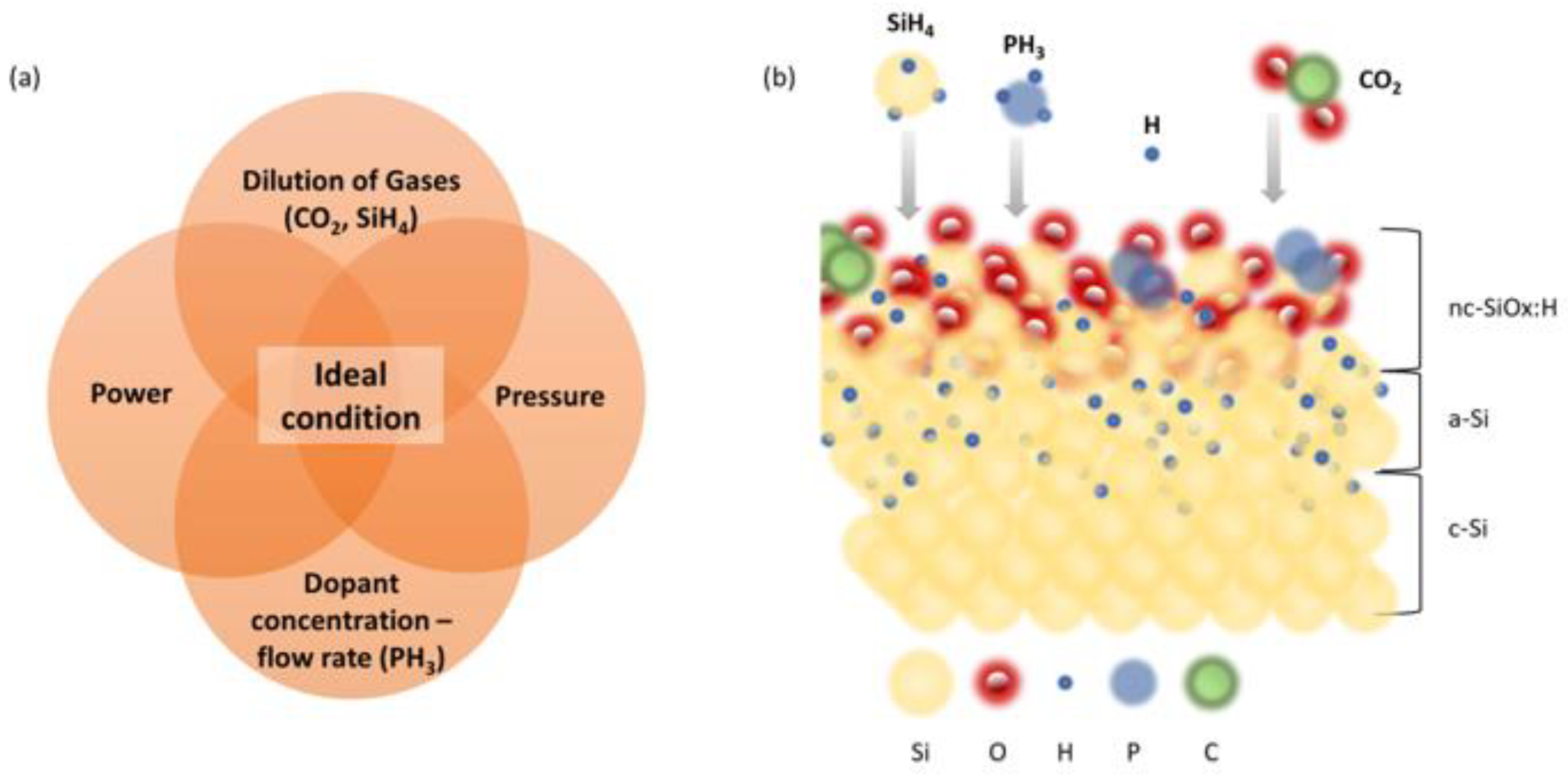
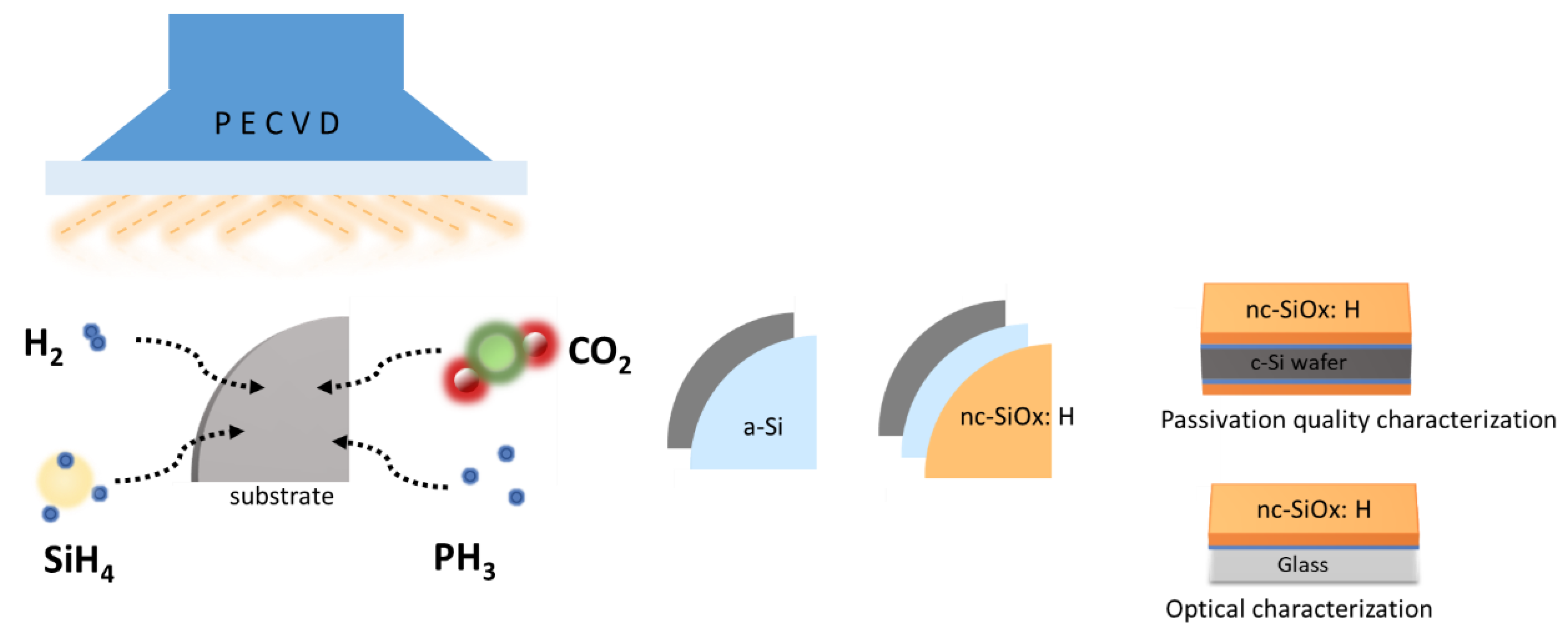
2. Materials and Methods

N-type nc-SiOx:H layers were deposited in an industrial-grade, plasma-enhanced chemical vapor deposition system, PECVD, (IndeoTec Octopus) on 1/4 of 4-inch, n-type FZ c-Si wafers with a resistivity of 1–3 Ω.cm and Corning glass. N-type FZ c-Si wafers were dipped in 5% HF solution for 30 s to remove the native oxide before introducing them in the PECVD chamber. A mixture of silane (SiH4), dihydrogen (H2), and carbon dioxide (CO2) was used as precursor for the deposition as shown in Figure 2. For n-type doping, 1% phosphorus (PH3) diluted in hydrogen was utilized. Typical deposition parameters were a pressure of 2.5 Torr, a substrate temperature of 180 °C, a deposition time of 10 min, and a radio frequency power of 50 W. The flow rates for gases were as follows: SiH4, 2–8 sccm; CO2, 0–4 sccm; and PH3, 0.5–2 sccm. For all samples discussed in this manuscript, H2 flow rate was fixed at 500 sccm. Furthermore, the radio frequency (RF) plasma power and pressure were varied within 20 W–80 W and 1.4 Torr–3 Torr, respectively. It should be noted that in all cases, a thin layer of a-Si:H was deposited on a c-Si wafer at 25 W, 1.6 Torr for 30 sec in order to provide a better passivation of the c-Si before deposition of the nanocrystalline silicon oxide layers. The deposition time was fixed at 10 min. Note that we target thin films (in the range of 10 nm–45 nm) relevant for passivation layers in solar cells. Thicker layers could be better crystallized but are not useful because absorption would be too high.
In this work, minority carrier lifetime (τ) is used as a measure of passivation quality because it provides information about the recombination of minority carriers’ (photocarrier) lifetime at the surface of a semiconductor material. It is composed of the bulk lifetime and surface lifetime, which depend on the surface properties of the sample. In low-level injected material, where the number of minority carriers is less than the doping level, the lifetime is determined by the recombination rate (R), as expressed in Equation (1):
τ = n R
where τ is the minority carrier lifetime, and Δ n is the excess minority carrier concentration [22]. As per Equation (1), longer τ indicates better passivation, suggesting lower recombination rates at the surface. This means there is a higher probability of carriers reaching the electrical contacts before recombining, which contributes to an enhanced charge collection efficiency for solar cells. It should be noted that the terms ‘long lifetime’ and ‘high lifetime’ are used interchangeably when we discuss this. The effective minority carrier lifetime (τeff) of the symmetrical samples was determined using the photoconductance decay (PCD) method using Sinton Lifetime Tester. The as-deposited values extracted at a minority carrier injection level of 1015 cm−3 are reported. The PCD measurements were either performed in the transient mode for samples with τeff above ~100 μs and in the quasi-steady-state mode using a generalized analysis for samples with low τeff < 100 μs [23,24]. Similarly, 1-sun implied open-circuit voltage (iVoc) was also extracted. Thermal annealing was avoided in this study so that an additional step was evaded for industrial compatibility. Subsequently, the homogeneity of the passivation quality was also determined by photoluminescence (PL) images obtained using a BTi luminescence imaging system at 1 sun. Optical properties of the films were measured via spectroscopic ellipsometry (SE) in the spectral range [1.5 eV–5 eV] using a phase-modulated ellipsometer (UVISEL from HORIBA John-Yvon). We measured films on both c-Si and glass substrates. The ellipsometry data were modeled using Bruggeman effective medium approximation (BEMA) using the DeltaPsi2 software on c-Si substrates. The optical gap of the film, denoted by E04, was estimated as the photon energy at which the absorption coefficient was 104 cm−1. We used the E04 value to provide an estimation of the optical gap because it is simpler and less error-prone than the Tauc method. However, if we carefully estimate the Tauc gap of the film, we can easily find a linear relationship between E04 and the Tauc gap, as used in [25,26]. Raman spectroscopy was used to analyze nanocrystalline and amorphous silicon phases in the films. Raman spectra were obtained with Horiba Raman Microscope in the range of 350 cm−1–1100 cm−1 using a laser with a wavelength of 532 nm on silicon samples. Raman spectra of the n-layers deposited on Si samples were used to identify and distinguish the presence of amorphous silicon and crystalline silicon phases in the nc-SiOx:H films. Finally, scanning electron microscope (SEM) images were obtained using a Zeiss instrument (Merlin compact) at various magnifications, and we also used an energy-dispersive X-ray (EDX) tool to analyze the compositional changes at nanoscale level.

3. Results and Discussion

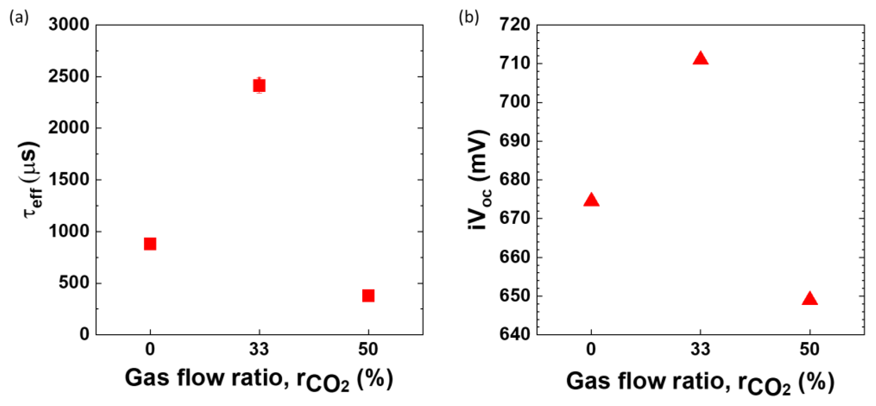
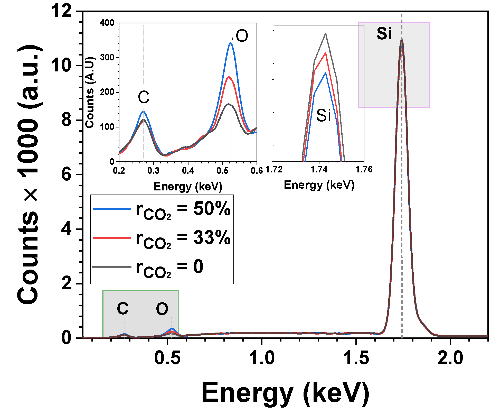
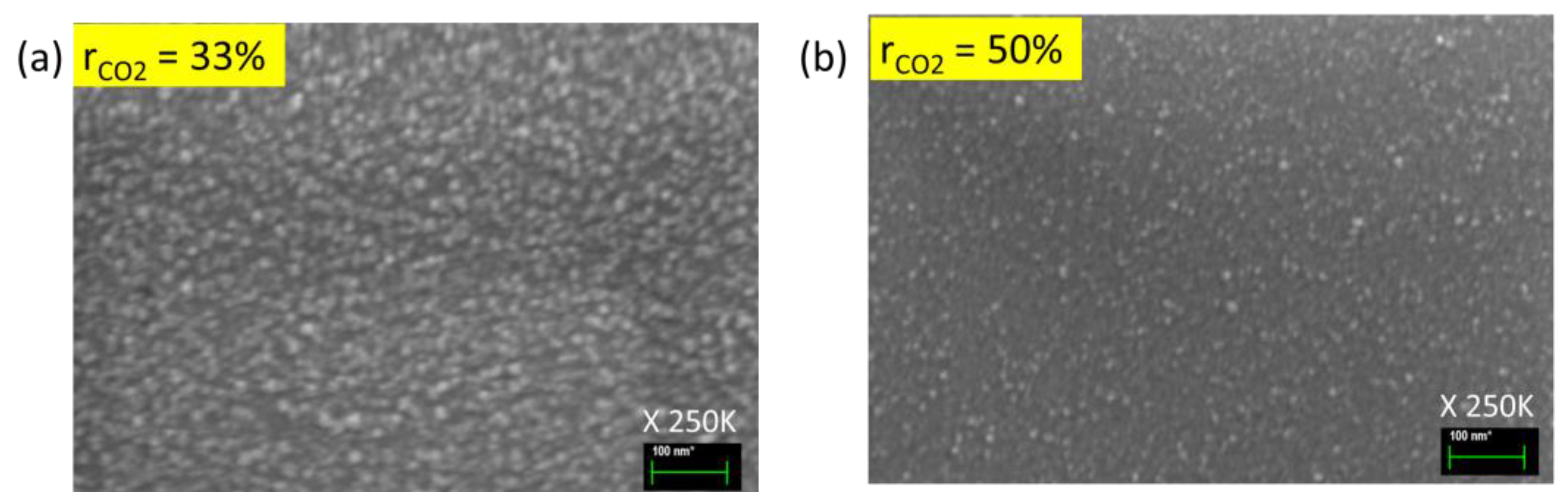
3.1. Optimization of Oxygen Content (CO2 Series)

Carbon dioxide (CO2) is used an oxygen precursor in the PECVD process for silicon oxide deposition, i.e., it provides oxygen for the formation of the silicon oxide film. The interaction of CO2 in the plasma generates reactive oxygen species that react with silicon precursors to form silicon oxide bonds. In this set, the CO2 flow rate was varied from 0–4 sccm in order to determine the optimum deposition conditions for the n-type nc-SiOx:H films. The deposition conditions used for these films were fixed as follows: PH3—0.8 sccm, SiH4—4 sccm, power—50 W, pressure—2.5 Torr. Figure 3 shows the effect of the CO2 flow rate on the passivation quality provided by n-type nc-SiOx:H films. The CO2 flow ratio is defined in Equation (2) as
r C O 2 = f C O 2 f S i H 4 + f C O 2   × 100
where f C O 2 and f S i H 4 are the CO2 and SiH4 gas flow rates, respectively. We started with r C O 2 = 0%, which means we are likely to obtain amorphous Si or n-type nc-Si:H films.
It can be observed that upon introduction of CO2 gas in the deposition chamber, there is an improvement in lifetime from 879 ± 31 μs to 2412 ± 72 μs. A similar trend was observed in iVoc values as well, increasing from 674.5 ± 0.5 mV to 710 ± 1 mV. However, too much CO2 in the chamber, i.e., increasing the gas flow ratio from 33% to 50%, results in deterioration of the lifetime and the passivation quality of the film (τeff = 377 ± 5 μs and iVoc = 649 mV).
In order to understand the dependence of the effective lifetime on the CO2 fraction, we analyzed the structural properties of the layers. Figure 4 displays the CO2 gas flow dependence on the material properties of n-type nc-SiOx:H films. EDX spectra show peaks at 0.27 eV, 0.53 eV, and 1.742 eV corresponding to carbon, oxygen, and silicon, respectively. It verifies that increasing the CO2 flow rate from 0% to 50% results in an augmentation of O content (from 165 counts → 245 counts → 342 counts) but a relative reduction in Si content (10,970 counts → 10,898 counts → 10,825 counts) within the films. We also observed an increase in the thickness of the films from 15.7 nm to 31.6 nm with a rise in r C O 2 . E04 values however, are in a similar ballpark, i.e., 2.16 eV for these samples.
In the plasma, CO2 splits into O and CO according to the reaction:
CO2 → CO + O
As the r C O 2 in the deposition chamber increases from 0% to 33%, the presence of CO and O is expected to increase in chamber as well as in the films as per Equation (3). According to the etching model of μc-Si:H formation, during the deposition process, atomic H reaching the film-growing surface weakens the Si–Si bond in the amorphous network, which can be replaced by stronger Si–O bonds due to presence of free O atoms/radicals, resulting in a greater likelihood for the Si–O–Si bond formation. Das et al. demonstrated that a higher concentration of atomic oxygen introduces additional structural defects [12], aiding merit to the above hypothesis.
When r C O 2 is further increased from 33% to 50%, more free oxygen forms stronger bonds with Si, forming more Si–O–Si bonds that are more energetically stable than Si–Si bonds. This reduces the etching potential due to higher hydrogen dilution, which can lead to an increased presence of O in the films, thicker layers due to the reduced etching, lower crystallinity, and, eventually, poor passivation quality, as seen in case of r C O 2 = 50% in Figure 3. Although most of the C is expected to leave the deposition chamber in the form of CO or CO2, a small amount is still embedded in the film [8,27]. Even in this case, at r C O 2 = 50%, C is incorporated in the deposited n-type nc-SiOx:H film (Figure 4), i.e., 144 counts compared to 121 counts in the case of r C O 2 = 0%. This could also be a reason for lower crystallinity at r C O 2 = 50%.
Scanning electron microscopy (SEM) images (Figure 5a,b) also confirm visually that the sample with CO2 flow rate 33% has more grains than its 50% counterpart. It has also been shown by Das et al. that an increase in the CO2 flow rate leads to a decrease in the grain size as well as the crystallite size in n-type μc-SiOx:H films [12]. This phenomenon is attributed to the elevated partial pressure of CO2 within the gas mixture, resulting in higher oxygen content in the films. The heightened presence of atomic oxygen introduces extra structural defects, thereby hindering the growth of crystallites and influencing their size [8]. Also, C gets incorporated in these n-type nc-SiOx:H films. On the other hand, Smirnov et al. and Shin et al. illustrated that extremely high O incorporation in the film can potentially cause an obstruction in the growth of crystallites, resulting in a very low dark conductivity [25,28].
The ability to control the O content in n-type nc-SiOx:H films offers a means to tailor their passivation quality and crystallinity, which are critical for enhancing the efficiency of solar cells. By optimizing the O content, it is possible to achieve improved passivation of crystalline silicon wafers, leading to reduced recombination rates at the surface and, consequently, higher τeff. This, in turn, can enhance the efficiency of carrier extraction in solar cells, ultimately contributing to improved overall device performance. Higher oxygen content ( r C O 2 = 33%) enhances the passivation quality of films and crystallinity. However, too much oxygen is detrimental for the overall quality of films. This is due to more incorporation of O in the films at even higher r C O 2   ( 50 % ) .   We obtain thicker films but with lower crystallinity and poor passivation quality. The relationship between the oxygen content, crystallinity, and passivation quality of n-type nc-SiOx:H films is a key factor in the development of advanced solar cell technologies, offering a pathway to enhance the efficiency and performance of solar energy conversion devices. Therefore, it is important to keep in mind the application of these passivating n-type nc-SiOx:H films while deciding the flow rate of CO2 gas. Since we are looking at films with high passivation quality, we choose r C O 2 = 33% for next set of experiments.

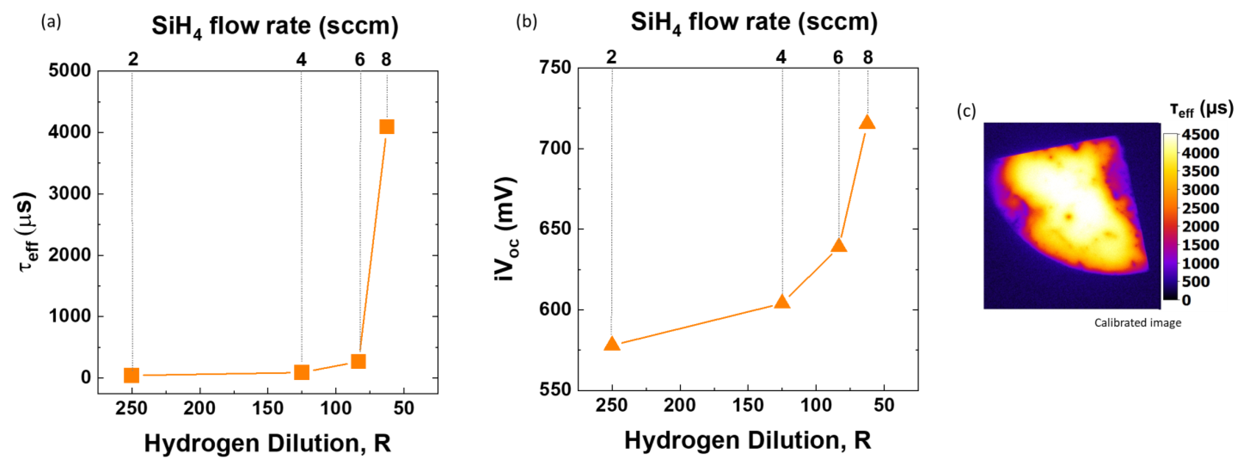
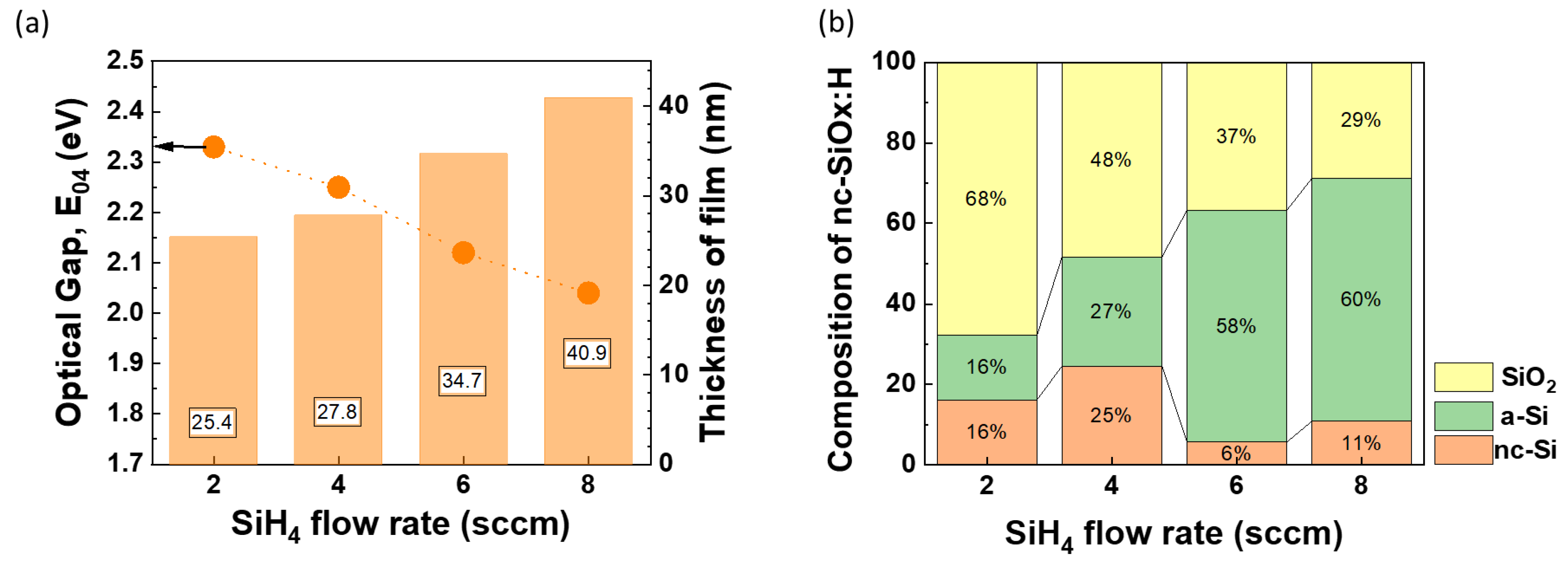
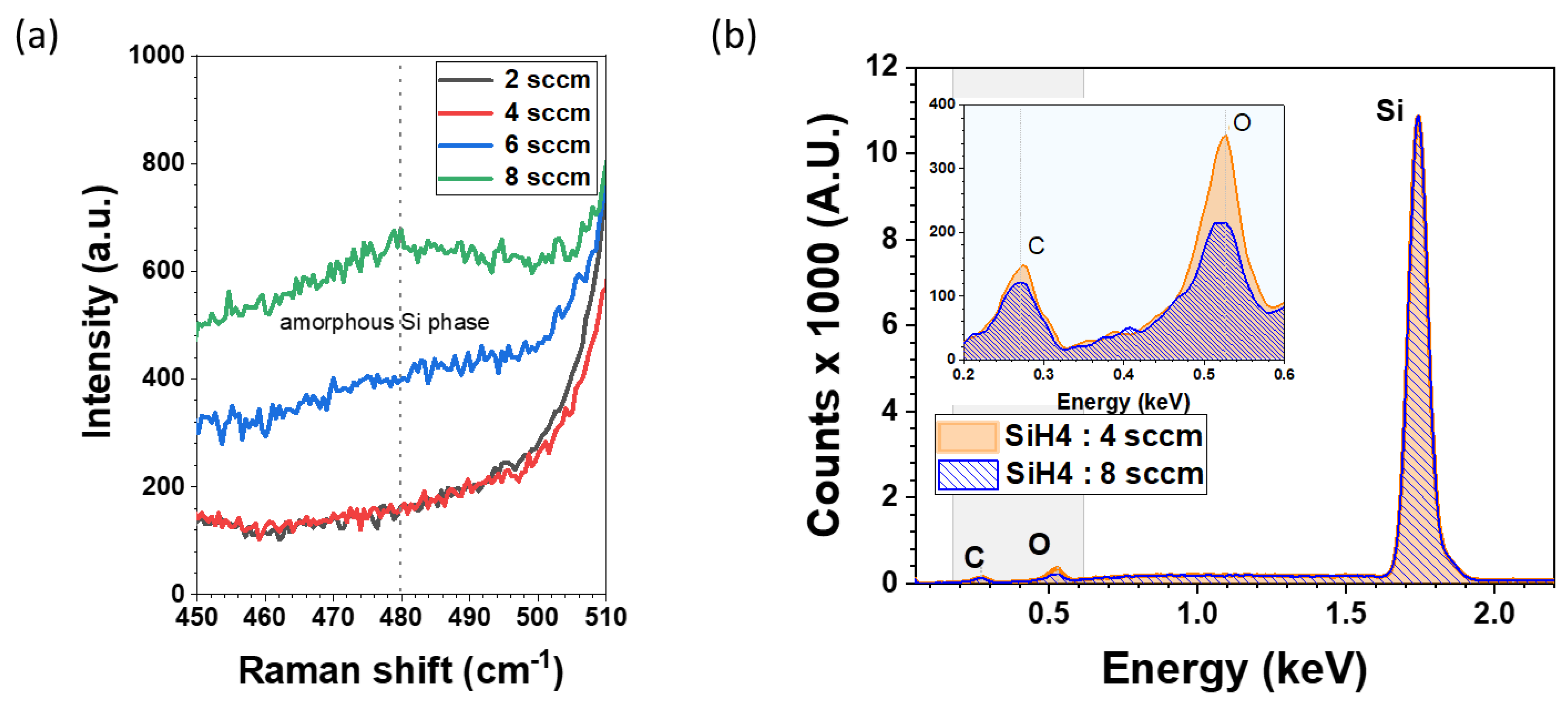
3.2. Optimization of SiH4 Series

Moving forward, we will explore the influence of the silane (SiH4) flow rate on the growth of our n-type nc-SiOx:H films. SiH4 serves as the silicon precursor, i.e., it provides the silicon component for the formation of the silicon oxide films. It undergoes dissociation in the plasma, and the resulting silicon species contribute to the deposition of the silicon oxide film. The incorporation of hydrogen from silane can also influence the hydrogenation level in the film, affecting its passivation. We will be using the hydrogen dilution parameter for ease of comparison, as most publications report this parameter. However, we also report the results with regards to the changing silane flow rate. It is generally understood that a higher hydrogen dilution is necessary to obtain nanocrystalline Si films. The hydrogen dilution ratio is described as R = [H2]/[SiH4], and the nature of the grown film depends strongly on this parameter. The deposition conditions used for these films were fixed as follows: CO2—2 sccm, PH3—0.8 sccm, power—50 W, pressure—2.5 Torr. As far as the passivation properties of the nanocrystalline silicon oxide films are concerned, we observe that upon decreasing the hydrogen dilution, the lifetime increases drastically from 42 μs (R = 250) to 4020 ± 71 μs (R = 62.5) (Figure 6a). Correspondingly, iVoc also mirrors this trend as it rises from 578 mV to 715.5 ± 0.5 mV, as shown in Figure 6b. The photoluminescence mapping in Figure 6c shows that the effective carrier lifetime is quite homogeneous over the quarter of wafer.
As the silane flow rate increases, we see an increase in thickness of the n-type nc-SiOx:H films from 25.4 nm to 40.9 nm and, hence, the deposition rate of films (Figure 7a). The optical gap of films also decreases steadily from 2.33 eV to 2.04 eV with an increase in the SiH4 flow rate (lower R) as shown in Figure 7.
Raman spectra of the films reveal c-Si peak at 520 cm−1, as the substrate was c-Si. The broader features observed around 480 cm−1 are attributed to an a-Si phase. Films with a low silane flow rate (2 sccm and 4 sccm), i.e., higher dilution (high R), show no presence of an a-Si phase. Raman data also illustrate that these n-type nc-SiOx:H films develop an amorphous phase when we increase the silane flow rate from 2 sccm to 8 sccm (Figure 8a). The composition of the films obtained from BEMA modelling (Figure 7b) also shows rise in the a-Si fraction from 16% to 60% with a corresponding surge in flow rate from 2 sccm to 8 sccm. SEM imaging on the 2 sccm sample revealed the existence of very small grains. The elemental EDX analysis (Figure 8b) of the n-type nc-SiOx:H films deposited at a SiH4 flow rate of 4 sccm reveals higher levels of elemental C (148 counts) and O (351 counts) compared to those of its 8 sccm counterpart (C = 121 counts and O = 214 counts). Figure 7b also indicates a higher presence of the SiO2 phase (4 sccm—48%, 8 sccm—29%) and nc-Si phase (4 sccm—25%, 8 sccm—11%) in the 4 sccm sample compared to its 8 sccm counterpart. In contrast for samples with an 8 sccm flow rate, the a-Si phase is more dominant, i.e., 60% compared to 27% (Figure 9). It implies that relatively higher hydrogen dilution is required for achieving better micro-crystallinity, whereas low hydrogen dilution is needed for producing amorphous nc-SiOx:H films.
Given the high E04 values at high R (low SiH4 flow rate), these films are well-suited to be used as back reflector or window layer, whereas films at low R (high SiH4 flow rate) can act as a passivating contact or even recombination layers in solar cells. Since we focus on highly passivating layers, we chose the SiH4 flow rate 8 sccm for the next set.

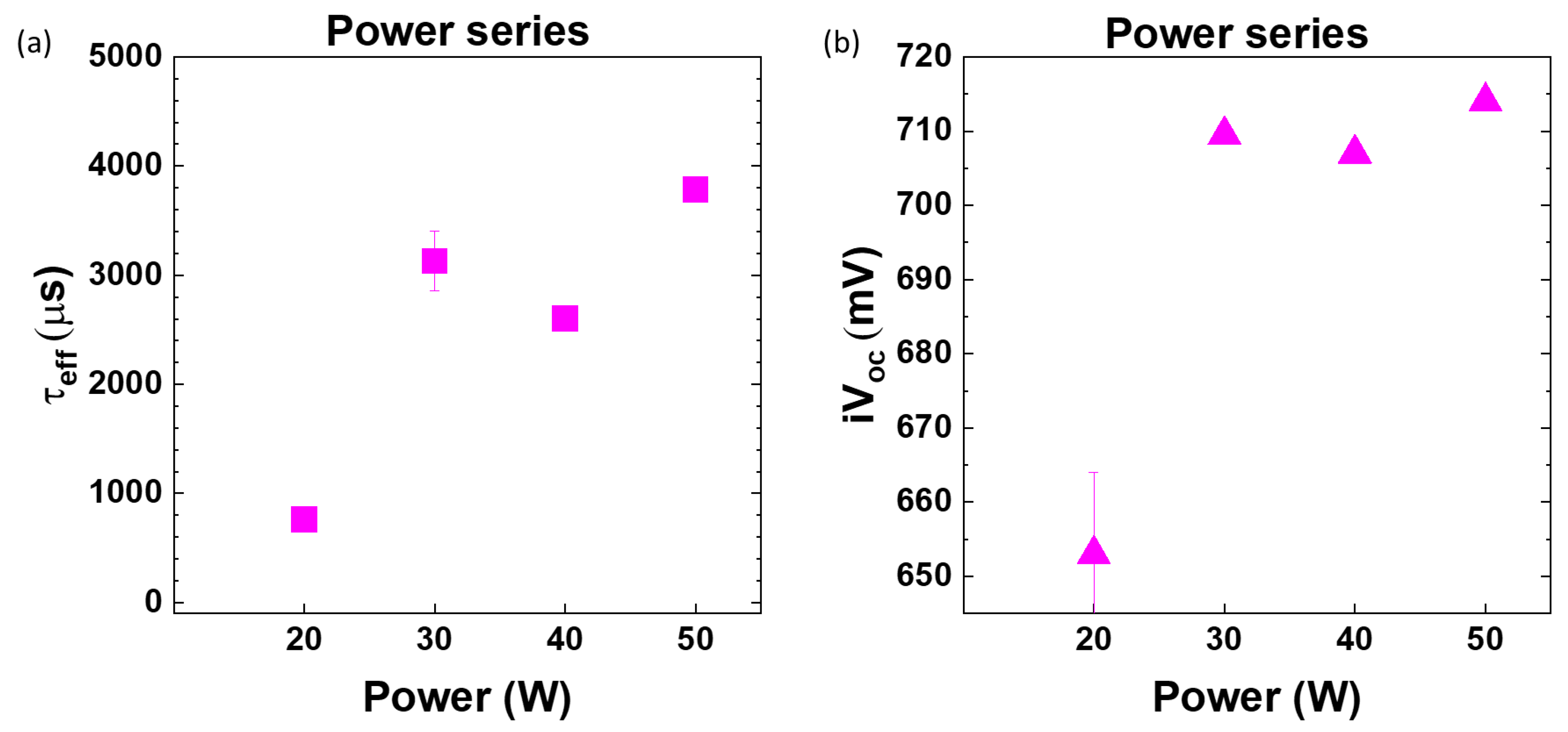
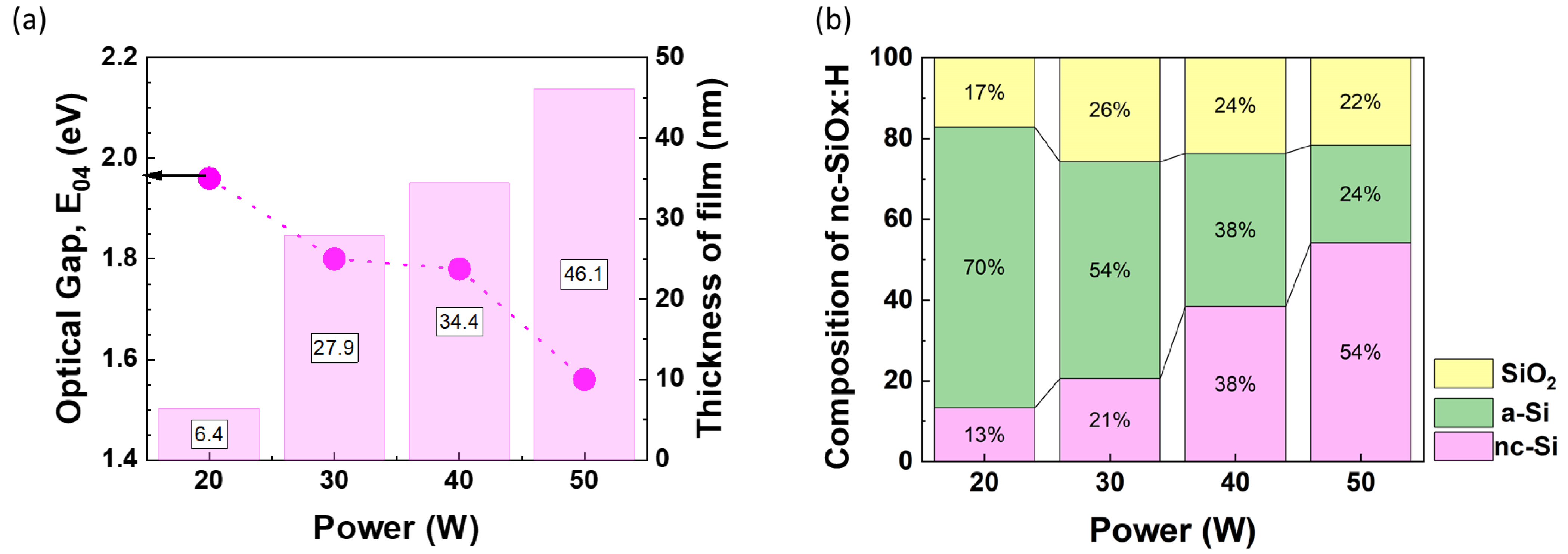
3.3. Optimization of RF Power

Radio frequency (RF) power is another important parameter that affects the dissociation of precursors and, therefore, the film composition. It is known that at a given set of deposition conditions, an increase in ion energy on the substrate may lead to defects and be potentially harmful to the interface [29]. In contrast, because of the increased surface mobility of reactive species, a sufficiently low level of ion bombardment is deemed to be beneficial for growth. Therefore, it is imperative for us to understand the role of power in determining passivation properties and doping nanocrystalline thin films. The deposition conditions for this set are CO2—2 sccm, PH3—0.8 sccm, SiH4—8 sccm, pressure—2.5 Torr.
As the RF power is reduced from 50 W to 20 W, a decline in the passivation properties of the films is observed, with a decrease from 3784 ± 99 μs at 50 W to 759 ± 112 μs at 20 W (Figure 9). The lower passivation at 20 W may be attributed to the deposition of films with a higher susceptibility to defects within the initial few nanometers of growth at lower power, considering the film’s thickness is only 6.4 nm (refer to Figure 10a). Concurrently, iVoc exhibits an increase from 653 ± 11 mV at lower power (20 W) to 714 ± 1 mV when the power is elevated to 50 W. Additional investigations were conducted at power levels exceeding 50 W (specifically, 60 W, 70 W, and 80 W). Nevertheless, the passivation quality, as indicated by both the effective lifetime (τeff) and iVoc, systematically deteriorates beyond 50 W, which could be attributed to excessive ion bombardment energy (plot in Supplementary Section-Figure S3).
Figure 10 shows that as we decrease the power from 50 W to 20 W, the optical gap of the films increases from 1.56 eV to 1.96 eV. Moreover, a decrease in power also results in a significant drop in the crystalline fraction from 54% to 13%, accompanied by an increase in the a-Si fraction from 24% to 70%. This can be attributed to the fact that at low power, the H2 dissociation and H production required for the nucleation of crystallites is not enough. A similar trend was reported by Juneja et al. based on Raman spectroscopy and SEM images [30]. Higher power promotes the decomposition of silane (SiH4) and hydrogen (H2), generating radicals like SiHx and atomic hydrogen. SiH3 specifically acts as a film-forming precursor, and atomic hydrogen promotes the nucleation of a crystalline phase and enhances precursor diffusion on the growing surface [31]. It has been reported that higher applied power favors microcrystalline/nanocrystalline growth [25,32].
Overall optimized power results from a tradeoff between the generation of a high-density plasma and low-energy ions, which result in the deposition of a highly crystalline structure. In order to form good nanocrystalline silicon oxide films, we need good passivation, crystallinity, as well as absorption (i.e., high lifetime, high crystalline fraction, and E04 closer to 2 eV). Therefore, we chose a RF power of 30 W for the next set.

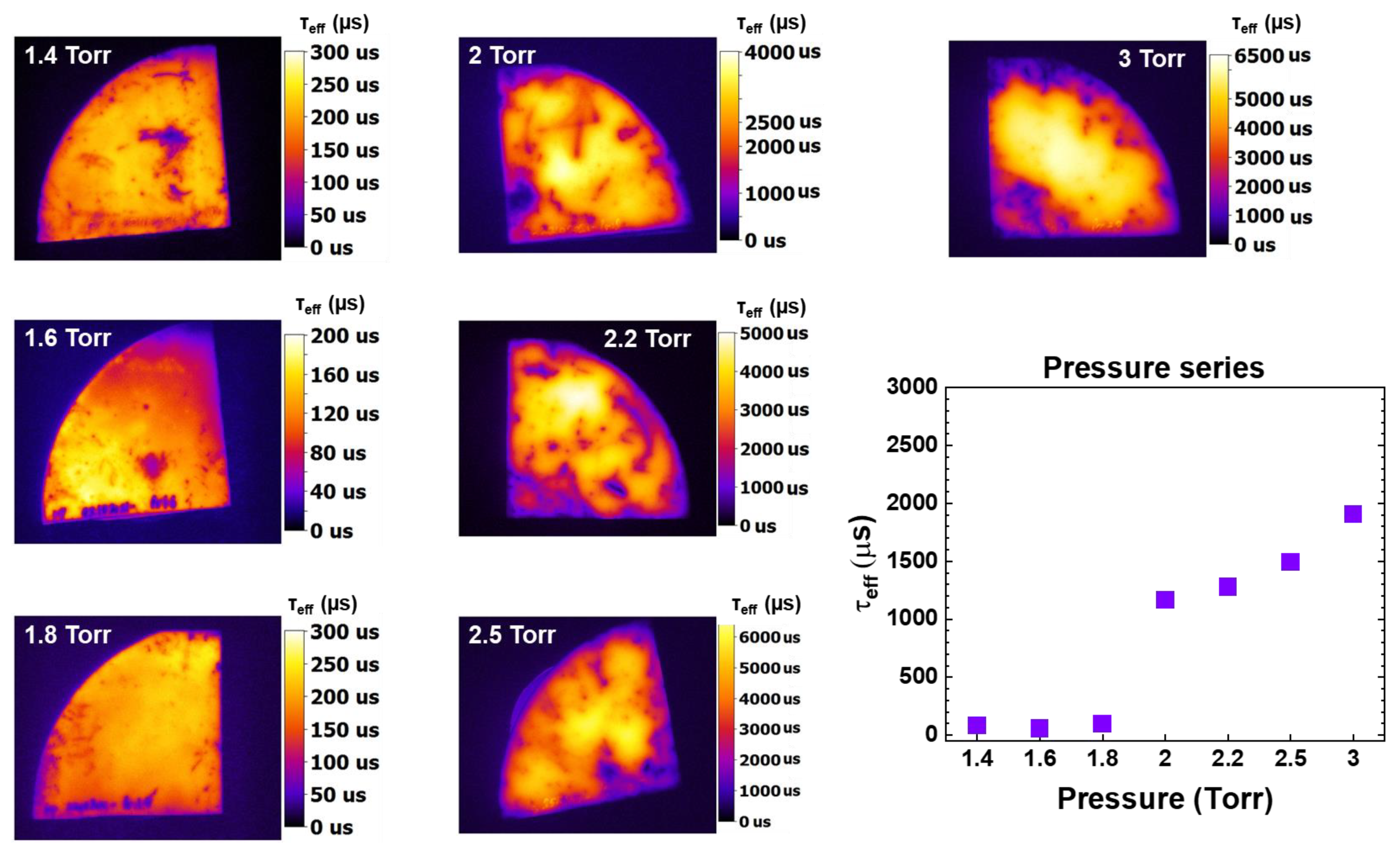
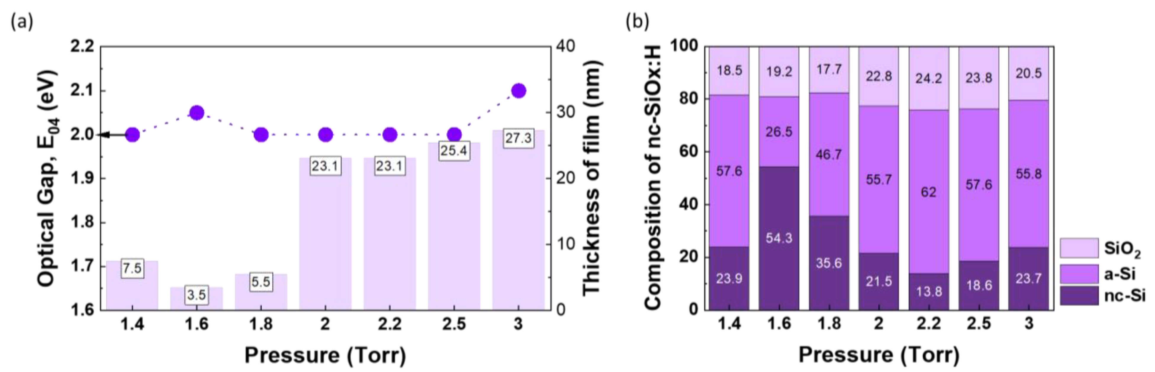
3.4. Optimization of Total Pressure

The deposition conditions for this set are CO2: 2 sccm, PH3: 0.8 sccm, SiH4: 8 sccm, power: 30 W. Figure 11 clearly shows a positive correlation between the pressure and passivation quality provided by nanocrystalline silicon oxide films. Higher chamber pressure results in higher lifetime. For deposition pressure values between 1.4 Torr and 1.8 Torr, the passivation quality is rather low (less than 300 μs). It is only at 2 Torr and above that the passivation quality of the samples improves, with the sample deposited at 3 Torr showing the highest passivation quality. However, because some powder formation was observed on the sample at such a high pressure, we preferred 2.5 Torr for sample deposition.
Figure 12 gives us an insight into this. At low chamber pressure (1.4 Torr–1.8 Torr), we observe that very thin films (3.3 nm–7.5 nm) are formed. It is only at 2 Torr that the deposition rate of the films takes off, resulting in about three-times-thicker films (~23 nm–27 nm). This is consistent with the low lifetime values, as well (Figure 11). It is known that silane dissociation by electron impact and the reaction H+SiH4 = SiH3+H2 are the main channels that produce SiH3 radicals. Below 2 Torr, the deposition rate is attributed to the increase in the dissociation of rate of SiH4 and H2. Between 2 and 2.5 Torr, as the deposition pressure increases, we see a decrease in the nc-Si phase from 21.5% to 18.6%. This trend has also been reported in our previous work on p-uc-SiOx:H films [33] and independently by Gabriel et al. [34]. This is because the deposition rate decreases due to SiH3 radicals and is dominated by the production of H3+ ions and its thermal fluxes according to the equations shown below [35,36,37,38]:
H2 + e = H2+ + 2e
H2 + H2+ = H3+ + H
At 3 Torr, we obtain a slightly higher E04 (2.1 eV) and nc-Si phase (~23.7%). Zhang et al. reported that 2.5 Torr is the critical gas pressure where the ionization of H2+ meets the energy threshold, so the production H3+ ions decreases even though the collision frequency still increases [38]. Therefore, H2+ ions’ production and their thermal fluxes dominate the H3+ ions’ production (according to Equation (5)) and their fluxes, resulting in a higher crystalline fraction and higher disorder.
Therefore, relatively low power (30 W) and high pressure (2.5 Torr) work best for passivating crystalline films that are suitable for application in silicon heterojunction devices and perovskite/silicon tandem solar cells.

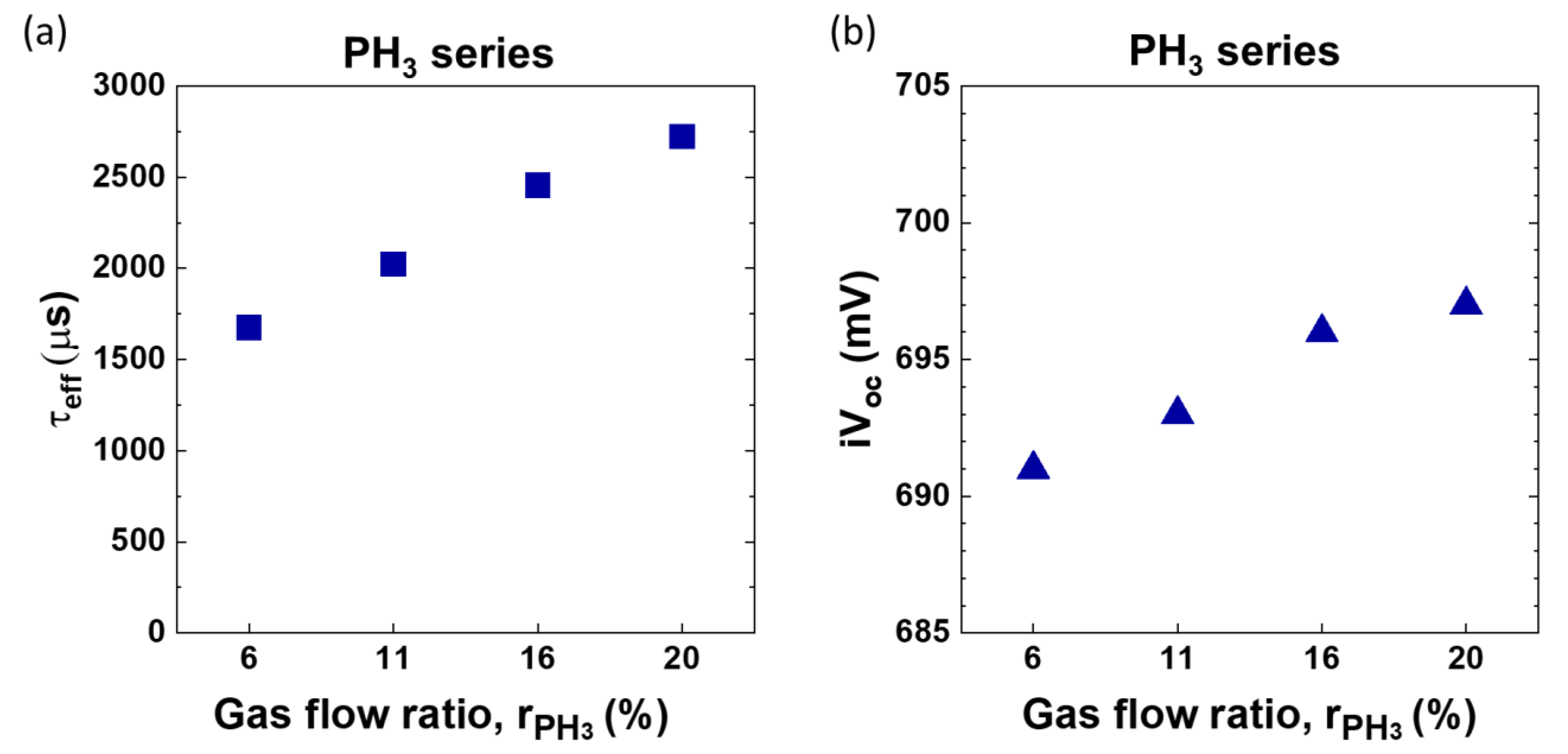
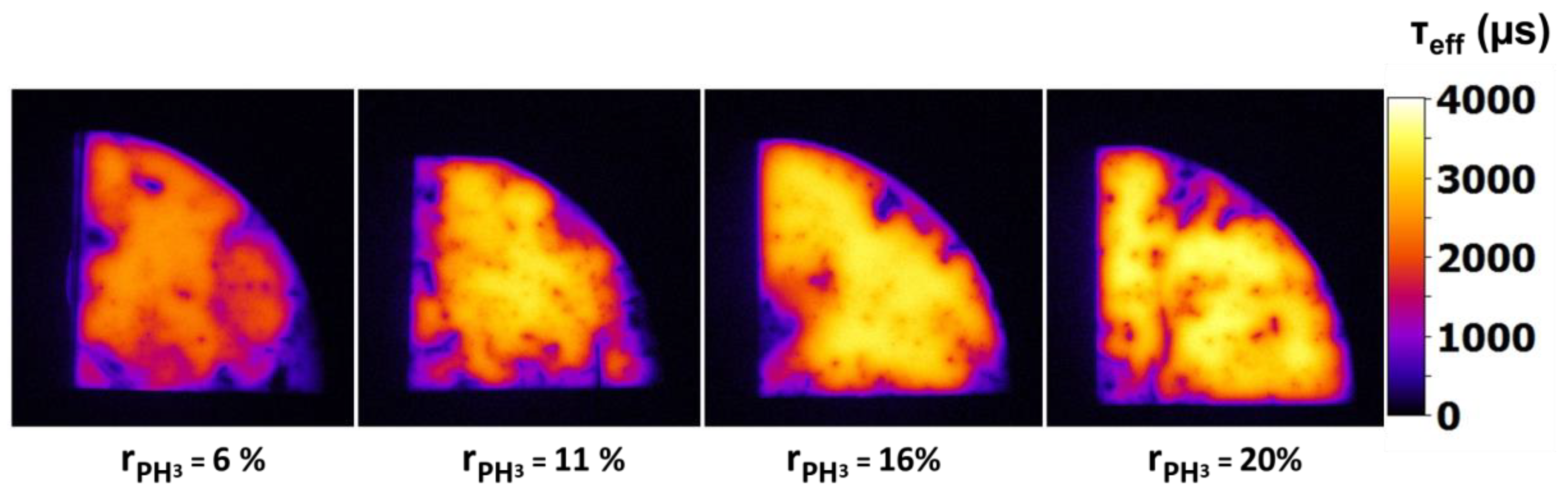
3.5. Optimization of Phosphine Flow Rate (PH3 Series)

As we know, PH3 is a dopant precursor and is used when doping of the nc-SiOx:H film with phosphorus is required. The addition of phosphorus can modify the electrical properties of the film, influencing its conductivity or other characteristics. Therefore, we made films with various values of the phosphine doping ratio by varying the PH3 flow ratio. The PH3 flow ratio ( r P H 3 ) is defined in Equation (6) as
r P H 3 = f P H 3 f S i H 4 + f P H 3 100
where fPH3 and fSiH4 are the PH3 and SiH4 gas flow rates, respectively. The PH3 gas was used as a source of phosphor atoms. Please note that PH3 is diluted at 1% in H2. The deposition conditions for these films were fixed as follows: CO2—2 sccm, SiH4—8 sccm, power—30 W, pressure—2.5 Torr. Usually, the doping atoms are smaller in number, so it is expected that the crystallinity of the deposited film will not change significantly with the addition of PH3. However, we do see a change in the passivation quality of the films. Figure 13 shows that upon increasing the flow of PH3 gas, there is an increase in the passivation quality. τeff improves from 1673 μs for r P H 3 = 6% to 2721 μs for r P H 3 = 20%, and iVoc follows a similar trend, which can be related to an increased field effect passivation. For r P H 3 = 20%, an iVoc of 697 mV is observed. It should be noted that overall, a uniform passivation with a lifetime in the range of 3.5 ms can be observed on the sample with r P H 3 = 20%, as shown by PL imaging in Figure 14.
The adaptability of hydrogenated nanocrystalline (nc-SiOx:H) material deposited by industrial, high-throughput PECVD for photovoltaic applications has been discussed in this work. In addition to talking about how pressure, power, and precursor gases (SiH4, CO2, and PH3) affect the optical and structural characteristics of deposited n-type nc-SiOx:H films, we also emphasized the significance of passivation qualities when tailoring their development. These n-type nc-SiOx:H films have a tunable optical gap range of 1.8–2.3 eV and excellent passivation properties (τeff up to 4.1 ms, iVoc~715.5 mV) achieved before annealing. Bearing in mind different applications such as front contacts, back reflectors, and intermediate window layers, it is evident that for the application of n-type, nc-SiOx:H films in solar cells, there is a trade-off between electrical (τeff and iVoc), structural (crystalline fraction), and optical properties (optical gap, E04). Meanwhile, n-type nc-SiOx:H films with a high E04 are favorable for window layers or intermediate reflectors, as their passivation properties are poor. On the contrary, films with high passivation properties and a low E04 are more suited for front contact or even recombination junction layers in tandem solar cells. Given the role oxygen plays in controlling the defect structure and absorption in the films, r C O 2 is a convenient parameter to vary the microstructure as well as the passivation and optical properties of these films. Both the RF power and pressure play an important role in determining the crystalline fraction of the films and control the amorphous and crystallite phases. Relatively low power (30 W) and high pressure (2.5 Torr) works best for passivating crystalline films suitable for application in silicon heterojunction devices and even perovskite/silicon tandem solar cells. Our results suggest that the properties of n-doped nc-SiOx:H films can be conveniently adjusted to fulfil various requirements as a front contact, intermediate layer, and back reflector.
Furthermore, here are practical insights based on our work that researchers and industry professionals can use to tailor the development of n-type nc-SiOx:H layers to meet the specific requirements of different solar cell applications:
  • Fine-tune the r C O 2 ratio to achieve the desired balance between passivation quality and crystallinity, considering the specific requirements of the solar cell application.
  • Controlling the dilution rate (R) during deposition allows for tuning of the hydrogen content in the film for effective passivation.
  • Tailor the r P H 3 to achieve the desired doping level for specific solar cell designs, ensuring optimal passivation properties without introducing excessive defects.
  • Choose an appropriate plasma property (power and pressure) based on the desired balance between crystallinity and passivation.

4. Conclusions

This work focused on optimizing the deposition conditions for n-type nanocrystalline silicon oxide (nc-SiOx:H) films, aiming at enhancing their potential for applications in silicon heterojunction devices and tandem cells as a front contact, intermediate layer, and back reflector. The study systematically explored various deposition parameters, including carbon dioxide (CO2) flow, silane (SiH4) flow, RF power, total pressure, and phosphine (PH3) doping, to understand their individual and collective impacts on film properties. In the investigation of CO2 flow, it was observed that a 33% CO2 flow ratio positively influenced the minority carrier lifetime (τeff = 2412 ± 27.5 μs) and open-circuit voltage (iVoc = 711 ± 1 mV), indicating improved passivation quality. However, increasing the CO2 flow ratio to 50% resulted in a decline in both τeff and iVoc, suggesting a delicate balance. The introduction of atomic oxygen from CO2 influenced the film morphology and composition, impacting crystallite growth and overall passivation quality. Silane (SiH4) flow was then studied, revealing that higher hydrogen dilution (lower R values) led to a transition from microcrystalline to amorphous phases. An increase in the SiH4 flow (8 sccm) resulted in lower oxygen incorporation, as indicated by a decrease in the optical gap (2.04 eV). This sample also showed a τeff as high as 4.1 ms (iVoc = 715.5 mV) before annealing. Raman spectra supported these findings, showing shifts in the crystalline and amorphous Si phases. Power optimization was explored, highlighting that power in the range of 30–50 W struck a balance between passivation, crystallinity, and absorption. Films deposited at medium powers exhibited better passivation properties, while powers above 50 W led to increased defects and lower crystallinity. Pressure variation demonstrated a positive correlation between higher pressure and improved passivation quality. Films deposited at 2.5 Torr showed the best properties, indicating the importance of deposition conditions in achieving optimal film characteristics. Lastly, phosphine (PH3) doping was investigated, showing that increasing PH3 flow rates improved passivation quality, as seen in the increased τeff and iVoc, probably related to enhanced field effect passivation. Overall, the optimal deposition conditions were identified as a 33% CO2 flow ratio, 8 sccm SiH4 flow, 30 W power, 2.5 Torr pressure, and 20% PH3 flow ratio for doping. These conditions aim to strike a balance between passivation quality, crystallinity, and absorption for potential applications in solar cell technology. Further studies on conductivity and crystalline volume fraction are suggested for a more comprehensive understanding of material properties and practical applications in solar cell technology. Overall, this research contributes valuable insights to the ongoing development of efficient thin-film solar cell technology.

Supplementary Materials

The following supporting information can be downloaded at: https://www.mdpi.com/article/10.3390/solar4010007/s1, Figure S1: Variation in minority carrier lifetime (τeff) w.r.t. minority carrier density of nc-SiOx:H films deposited with changing CO2 gas flow ratio, Figure S2: Variation in minority carrier lifetime (τeff) w.r.t. minority carrier density of nc-SiOx:H films deposited with changing PH3 gas flow ratio, Figure S3: (a) Effective minority carrier lifetime (τeff) and (b) implied Voc (iVoc) of nanocrystalline silicon oxide (nc-SiOx:H) films deposited at various powers (20–80 W).

Author Contributions

Conceptualization: G.K. and P.R.i.C.; methodology and experiment design: G.K.; data collection and analysis: G.K. and A.J.O.; software analysis: G.K. and A.J.O.; validation: G.K. and P.R.i.C.; writing—original draft preparation: G.K.; writing—review and editing: G.K., A.J.O. and P.R.i.C.; visualization, G.K.; supervision: P.R.i.C.; project administration: P.R.i.C.; funding acquisition: P.R.i.C. All authors have read and agreed to the published version of the manuscript.

Funding

This work was partially funded by the SOLAR-ERA.NET project “CUSTCO” ANR-19-SOL2-0002-04 of the French Research National Agency (ANR) as well as by the French Government in the frame of the program of investment for the future (Programme d’Investissement d’Avenir-ANR-IEED-002-01).

Institutional Review Board Statement

Not applicable.

Informed Consent Statement

Not applicable.

Data Availability Statement

The data that support the findings of this study are available from the corresponding authors upon reasonable request.

Acknowledgments

Authors would like to thank funding by Institut Photovoltaïque d’Ile-de-France (IPVF) and Laboratoire de Physique des Interfaces et des Couches Minces (LPICM) for their support.

Conflicts of Interest

The authors declare no conflicts of interest.

References

  1. Mazzarella, L.; Morales-Vilches, A.; Korte, L.; Schlatmann, R.; Stannowski, B. Versatility of Nanocrystalline Silicon Films: From Thin-Film to Perovskite/c-Si Tandem Solar Cell Applications. Coatings 2020, 10, 759. [Google Scholar] [CrossRef]
  2. Cuony, P.; Marending, M.; Alexander, D.T.L.; Boccard, M.; Bugnon, G.; Despeisse, M.; Ballif, C. Mixed-phase p-type silicon oxide containing silicon nanocrystals and its role in thin-film silicon solar cells. Appl. Phys. Lett. 2010, 97, 213502. [Google Scholar] [CrossRef]
  3. Cuony, P.; Alexander, D.T.L.; Perez-Wurfl, I.; Despeisse, M.; Bugnon, G.; Boccard, M.; Söderström, T.; Hessler-Wyser, A.; Hébert, C.; Ballif, C. Silicon Filaments in Silicon Oxide for Next-Generation Photovoltaics. Adv. Mater. 2012, 24, 1182–1186. [Google Scholar] [CrossRef]
  4. Ding, K.; Aeberhard, U.; Smirnov, V.; Holländer, B.; Finger, F.; Rau, U. Wide Gap Microcrystalline Silicon Oxide Emitter for a-SiOx:H/c-Si Heterojunction Solar Cells. Jpn. J. Appl. Phys. 2013, 52, 122304. [Google Scholar] [CrossRef]
  5. Ding, K.; Aeberhard, U.; Lambertz, A.; Smirnov, V.; Holländer, B.; Finger, F.; Rau, U. Impact of doped microcrystalline silicon oxide layers on crystalline silicon surface passivation. Can. J. Phys. 2014, 92, 758–762. [Google Scholar] [CrossRef]
  6. Lambertz, A.; Grundler, T.; Finger, F. Hydrogenated amorphous silicon oxide containing a microcrystalline silicon phase and usage as an intermediate reflector in thin-film silicon solar cells. J. Appl. Phys. 2011, 109, 113109. [Google Scholar] [CrossRef]
  7. Lambertz, A. Development of Doped Microcrystalline Silicon Oxide andits Application to Thin-Film Silicon Solar Cells, University Utrecht. 2015. Available online: https://juser.fz-juelich.de/record/190115/export/he?ln=en (accessed on 9 June 2023).
  8. Richter, A.; Smirnov, V.; Lambertz, A.; Nomoto, K.; Welter, K.; Ding, K. Versatility of doped nanocrystalline silicon oxide for applications in silicon thin-film and heterojunction solar cells. Sol. Energy Mater. Sol. Cells 2018, 174, 196–201. [Google Scholar] [CrossRef]
  9. Smirnov, V.; Böttler, W.; Lambertz, A.; Wang, H.; Carius, R.; Finger, F. Microcrystalline silicon n-i-p solar cells prepared with microcrystalline silicon oxide (μc-SiOx:H) n-layer. Phys. Status Solidi C 2010, 7, 1053–1056. [Google Scholar] [CrossRef]
  10. Smirnov, V.; Lambertz, A.; Grootoonk, B.; Carius, R.; Finger, F. Microcrystalline silicon oxide (μc-SiOx:H) alloys: A versatile material for application in thin film silicon single and tandem junction solar cells. J. Non-Cryst. Solids 2012, 358, 1954–1957. [Google Scholar] [CrossRef]
  11. Smirnov, V.; Boettler, W.; Lambertz, A.; Astakhov, O.; Carius, R.; Finger, F. N-type Microcrystalline Silicon Oxide (μc-SiOx:H) Window Layers with Combined Anti-reflection Effects for n-i-p Thin Film Silicon Solar Cells. MRS Proc. 2010, 1245, 2102. [Google Scholar] [CrossRef]
  12. Das, G.; Mandal, S.; Dhar, S.; Bose, S.; Mukhopadhyay, S.; Banerjee, C.; Barua, A.K. Development of n-type microcrystalline SiOx:H films and its application by innovative way to improve the performance of single junction µc-Si:H solar cell. J. Mater. Sci. Mater. Electron. 2017, 28, 5746–5753. [Google Scholar] [CrossRef]
  13. Mazzarella, L.; Morales-Vilches, A.B.; Hendrichs, M.; Kirner, S.; Korte, L.; Schlatmann, R.; Stannowski, B. Nanocrystalline n-Type Silicon Oxide Front Contacts for Silicon Heterojunction Solar Cells: Photocurrent Enhancement on Planar and Textured Substrates. IEEE J. Photovolt. 2018, 8, 70–78. [Google Scholar] [CrossRef]
  14. Olivares, A.J.; Seif, J.P.; Repecaud, P.-A.; Longeaud, C.; Morales-Masis, M.; Bivour, M.; Roca i Cabarrocas, P. Highly conductive p-type nc-SiOX:H thin films deposited at 130 °C via efficient incorporation of plasma synthesized silicon nanocrystals and their application in SHJ solar cells. Sol. Energy Mater. Sol. Cells 2024, 266, 112675. [Google Scholar] [CrossRef]
  15. Mazzarella, L.; Morales-Vilches, A.B.; Korte, L.; Schlatmann, R.; Stannowski, B. Ultra-thin nanocrystalline n-type silicon oxide front contact layers for rear-emitter silicon heterojunction solar cells. Sol. Energy Mater. Sol. Cells 2018, 179, 386–391. [Google Scholar] [CrossRef]
  16. Qiu, D.; Duan, W.; Lambertz, A.; Bittkau, K.; Steuter, P.; Liu, Y.; Gad, A.; Pomaska, M.; Rau, U.; Ding, K. Front contact optimization for rear-junction SHJ solar cells with ultra-thin n-type nanocrystalline silicon oxide. Sol. Energy Mater. Sol. Cells 2020, 209, 110471. [Google Scholar] [CrossRef]
  17. Smirnov, V.; Lambertz, A.; Tillmanns, S.; Finger, F. p- and n-type microcrystalline silicon oxide (μc-SiOx:H) for applications in thin film silicon tandem solar cells. Can. J. Phys. 2014, 92, 932–935. [Google Scholar] [CrossRef]
  18. Khokhar, M.Q.; Chowdhury, S.; Pham, D.P.; Hussain, S.Q.; Cho, E.-C.; Yi, J. Improving passivation properties using a nano-crystalline silicon oxide layer for high-efficiency TOPCon cells. Infrared Phys. Technol. 2021, 115, 103723. [Google Scholar] [CrossRef]
  19. Kaur, G.; Xin, Z.; Dutta, T.; Sridharan, R.; Stangl, R.; Danner, A. Improved silicon oxide/polysilicon passivated contacts for high efficiency solar cells via optimized tunnel layer annealing. Sol. Energy Mater. Sol. Cells 2020, 217, 110720. [Google Scholar] [CrossRef]
  20. Mazzarella, L.; Werth, M.; Jäger, K.; Jošt, M.; Korte, L.; Albrecht, S.; Schlatmann, R.; Stannowski, B. Infrared photocurrent management in monolithic perovskite/silicon heterojunction tandem solar cells by using a nanocrystalline silicon oxide interlayer. Opt. Express 2018, 26, A487–A497. [Google Scholar] [CrossRef] [PubMed]
  21. Jäger, K.; Sutter, J.; Hammerschmidt, M.; Schneider, P.-I.; Becker, C. Prospects of light management in perovskite/silicon tandem solar cells. Nanophotonics 2020, 10, 1991–2000. [Google Scholar] [CrossRef]
  22. Sinton, R.A.; Swanson, R.M. Recombination in highly injected silicon. IEEE Trans. Electron Devices 1987, 34, 1380–1389. [Google Scholar] [CrossRef]
  23. Sinton, R.A.; Cuevas, A. Contactless determination of current–voltage characteristics and minority-carrier lifetimes in semiconductors from quasi-steady-state photoconductance data. Appl. Phys. Lett. 1996, 69, 2510–2512. [Google Scholar] [CrossRef]
  24. Richter, A.; Glunz, S.W.; Werner, F.; Schmidt, J.; Cuevas, A. Improved quantitative description of Auger recombination in crystalline silicon. Phys. Rev. B 2012, 86, 165202. [Google Scholar] [CrossRef]
  25. Shin, C.; Iftiquar, S.M.; Park, J.; Kim, Y.; Kim, S.; Jung, J.; Yi, J. Development of highly conducting n-type micro-crystalline silicon oxide thin film and its application in high efficiency amorphous silicon solar cell. Mater. Sci. Semicond. Process. 2017, 66, 223–231. [Google Scholar] [CrossRef]
  26. Saha, S.C.; Ray, S. Development of highly conductive n-type μc-Si:H films at low power for device applications. J. Appl. Phys. 1995, 78, 5713–5720. [Google Scholar] [CrossRef]
  27. Iftiquar, S.M. The roles of deposition pressure and rf power in opto-electronic properties of a-SiO:H films. J. Phys. Appl. Phys. 1998, 31, 1630–1641. [Google Scholar] [CrossRef]
  28. Smirnov, V.; Lambertz, A.; Finger, F. Electronic and Structural Properties of N-Type Microcrystalline Silicon Oxide (Mc Siox:H) Films for Applications in Thin Film Silicon Solar Cells. Energy Procedia 2015, 84, 71–77. [Google Scholar] [CrossRef]
  29. Bruneau, B.; Cariou, R.; Dornstetter, J.-C.; Lepecq, M.; Maurice, J.-L.; Roca i Cabarrocas, P.; Johnson, E.V. Ion Energy Threshold in Low-Temperature Silicon Epitaxy for Thin-Film Crystalline Photovoltaics. IEEE J. Photovolt. 2014, 4, 1361–1367. [Google Scholar] [CrossRef]
  30. Juneja, S.; Kumar, S. Effect of Power on Crystallinity and Opto-Electronic Properties of Silicon Thin Films Grown Using VHF PECVD Process. Silicon 2021, 13, 3927–3940. [Google Scholar] [CrossRef]
  31. Layadi, N.; Roca i Cabarrocas, P.; Drévillon, B.; Solomon, I. Real-time spectroscopic ellipsometry study of the growth of amorphous and microcrystalline silicon thin films prepared by alternating silicon deposition and hydrogen plasma treatment. Phys. Rev. B 1995, 52, 5136–5143. [Google Scholar] [CrossRef]
  32. Zhou, H.P.; Xu, M.; Xu, S.; Feng, Y.Y.; Xu, L.X.; Wei, D.Y.; Xiao, S.Q. A comparative study on the direct deposition of μc-Si:H and plasma-induced recrystallization of a-Si:H: Insight into Si crystallization in a high-density plasma. Appl. Surf. Sci. 2018, 433, 285–291. [Google Scholar] [CrossRef]
  33. Olivares, A.J.; Kaur, G.; Poplawski, M.; Desthieux, A.; Roca i Cabarrocas, P. Optimization of the Conductivity and Crystalline Fraction of p-Type μc-SiOx:H Films for Silicon Heterojunction Solar Cells. In Optimization of the Conductivity and Crystalline Fraction of p-Type μc-SiOx:H Films for Silicon Heterojunction Solar Cells; EUPVSEC Proceedings: Vienna, Austria, 2021; pp. 212–216. [Google Scholar] [CrossRef]
  34. Gabriel, O.; Kirner, S.; Klingsporn, M.; Friedrich, F.; Stannowski, B.; Schlatmann, R. On the Plasma Chemistry During Plasma Enhanced Chemical Vapor Deposition of Microcrystalline Silicon Oxides. Plasma Process. Polym. 2015, 12, 82–91. [Google Scholar] [CrossRef]
  35. Janev, R.K.; Langer, W.D.; Post, D.E.; Evans, K. Collision Processes and Reaction of H2+Ions. In Elementary Processes in Hydrogen-Helium Plasmas: Cross Sections and Reaction Rate Coefficients; Janev, R.K., Langer, W.D., Post, D.E., Evans, K., Eds.; Springer Series on Atoms+Plasmas; Springer: Berlin, Heidelberg, 1987; pp. 167–179. [Google Scholar] [CrossRef]
  36. Coltrin, M.E.; Kee, R.J.; Miller, J.A. A Mathematical Model of Silicon Chemical Vapor Deposition: Further Refinements and the Effects of Thermal Diffusion. J. Electrochem. Soc. 1986, 133, 1206. [Google Scholar] [CrossRef]
  37. Landheer, K.; Goedheer, W.J.; Poulios, I.; Schropp, R.E.I.; Rath, J.K. Chemical sputtering by H2+ and H3+ ions during silicon deposition. J. Appl. Phys. 2016, 120, 053304. [Google Scholar] [CrossRef]
  38. Zhang, T.; Orlac’h, J.-M.; Ghosh, M.; Giovangigli, V.; Roca i Cabarrocas, P.; Novikova, T. Role of H3+ ions in deposition of silicon thin films from SiH4/H2 discharges: Modeling and experiments. Plasma Sources Sci. Technol. 2021, 30, 075024. [Google Scholar] [CrossRef]
Figure 1. (a) Schematic of interdependence of deposition parameters for the growth of doped nc-SiOx:H films by the plasma-enhanced chemical vapor deposition system (PECVD) studied in this work. (b) Pictographic representation of surface growth reaction of nc-SiOx:H structure deposited using silane (SiH4), hydrogen (H2), carbon dioxide (CO2), and phosphine (PH3) as precursor gases. Each gas has a specific role in determining the composition, structure, and properties of the deposited film. Silane (SiH4) serves as the silicon (Si) precursor, whereas CO2 acts as the oxygen (O) precursor, and they provide Si and O, respectively, for the formation of silicon oxide in the PECVD process. The incorporation of hydrogen from SiH4 can also influence the hydrogenation level in the film, affecting its passivation properties. Phosphine (PH3) acts as the dopant precursor and introduces phosphorous (P) in the deposited silicon oxide films. The addition of phosphorus can modify the electrical properties of the film, influencing its conductivity or other characteristics. Hydrogen (H2) is commonly used as a co-reactant or reducing agent in the PECVD processes (also in our case). Chemical species shown in the image are for representation purposes only (not to scale).
Solar 04 00007 g001
Figure 2. Schematic of experimental process flow for depositing nc-SiOx:H films both on c-Si wafers and Corning glass substrates in the PECVD chamber. A thin buffer layer of a-Si:H was deposited on the substrate before depositing nc-SiOx:H films.
Solar 04 00007 g002
Figure 3. Variation in (a) effective minority carrier lifetime (τeff) and (b) implied open-circuit voltage (iVoc) of n-type nc-SiOx:H films deposited with changing CO2 gas flow ratio. Please note that the lifetime curves for these gas ratios can be found in supplementary section Figure S1.
Solar 04 00007 g003
Figure 4. Energy dispersive X-ray (EDX) spectra of n-type nc-SiOx:H layers deposited at different CO2 gas flow ratios. The inset is the magnification of C, O, and Si peaks.
Solar 04 00007 g004
Figure 5. Scanning electron microscopy (SEM) images of n-type nc-SiOx:H films deposited at CO2 gas flow ratios (a) 33% and (b) 50% at magnification ratio of 250 K.
Solar 04 00007 g005
Figure 6. Variation of electrical properties of n-type nc-SiOx:H films: (a) lifetime (τeff) and (b) implied open-circuit voltage (iVoc) with changing hydrogen dilution (R), i.e., by varying the SiH4 flow rate from 2 sccm to 8 sccm. (c) Calibrated PL image of sample deposited at SiH4 flow rate = 8 sccm (i.e., R = 62.5) at steady-state light intensity of 1 sun.
Solar 04 00007 g006
Figure 7. Impact of variation in silane (SiH4) flow rate (2–8 sccm) on (a) optical gap (E04) (data indicated by arrow and dots) and thickness of films (nm) is illustrated in columns. (b) Composition of n-type nanocrystalline silicon oxide (nc-SiOx:H) films.
Solar 04 00007 g007
Figure 8. (a) Raman spectra of n-type nanocrystalline silicon oxide (nc-SiOx:H) films deposited at varying silane flow rates (2–8 sccm) on c-Si. (b) Energy dispersive X-ray (EDX) elemental analysis of n-type nc-SiOx:H films deposited at silane flow rates of 4 sccm and 8 sccm.
Solar 04 00007 g008
Figure 9. (a) Effective minority carrier lifetime (τeff) and (b) implied Voc (iVoc) of n-type nanocrystalline silicon oxide (nc-SiOx:H) films deposited at various powers (20–50 W).
Solar 04 00007 g009
Figure 10. Comparison of n-type nc-SiOx:H films deposited at different power variations (20–50 W). (a) Optical gap (data indicated via an arrow) and thickness of films illustrated in columns; (b) structural composition of different phases of n-type nc-SiOx:H layers.
Solar 04 00007 g010
Figure 11. PL image map of n-type nc-SiOx:H films (on Si substrate) deposited at various values of pressure (1.4 Torr–3 Torr). It is calibrated to minority carrier lifetime (τeff)) at light intensity of 1 sun. Mean value of τeff from each sample is also extracted and plotted against each pressure condition.
Solar 04 00007 g011
Figure 12. Comparison of n-type nc-SiOx:H films deposited at different pressures (1.4 Torr–3 Torr). (a) Optical gap (data indicated by an arrow) and thickness of film illustrated in columns; (b) structural composition of different phases.
Solar 04 00007 g012
Figure 13. Variation in (a) minority carrier lifetime (τeff) and (b) implied open-circuit voltage (iVoc) with change in gas flow ratio of PH3. Please note that the lifetime curves for these gas ratios can be found in Supplementary Section Figure S2.
Solar 04 00007 g013
Figure 14. Photoluminescence (PL) image of n-type nc-SiOx:H samples deposited at different values of the PH3 gas flow ratio r P H 3 = 6%, 11%, 16%, and 20%. It is calibrated to lifetime at 1 sun.
Solar 04 00007 g014
Disclaimer/Publisher’s Note: The statements, opinions and data contained in all publications are solely those of the individual author(s) and contributor(s) and not of MDPI and/or the editor(s). MDPI and/or the editor(s) disclaim responsibility for any injury to people or property resulting from any ideas, methods, instructions or products referred to in the content.

