Article

Simulation of Lead-Free Heterojunction CsGeI2Br/CsGeI3-Based Perovskite Solar Cell Using SCAPS-1D

by
Abraham Dimitri Kapim Kenfack
1,*,
Nicolas Matome Thantsha
1 and
Mandla Msimanga
1,2
1
PV Nanocomposites R&D Platform, Department of Physics, Tshwane University of Technology, Private Bag X 60, Pretoria 0001, South Africa
2
NRF-iThemba LABS, Private Bag WITS 2050, Johannesburg 2017, South Africa
*
Author to whom correspondence should be addressed.
Solar 2023, 3(3), 458-472; https://doi.org/10.3390/solar3030025
Submission received: 26 June 2023 / Revised: 30 July 2023 / Accepted: 31 July 2023 / Published: 7 August 2023
(This article belongs to the Special Issue Developments in Perovskite Solar Cells)

Abstract

:
This paper presents the simulation of the novel prototype of a heterojunction perovskite solar cell (PSC) based on CSGeI2Br/CSGeI3. The device consists of two absorber layers (CSGeI2Br, CSGeI3), an electron transport layer (ETL) chosen as TiO2 and a hole transport layer (HTL) given as poly(3-hexylthiophene) (P3HT). Within the simulation, the effects of thickness, doping and defect density in each absorber layer and different back contact metal electrodes on electrical parameters (efficiency, short circuit current, open circuit voltage, and fill factor) are evaluated. In addition, the contribution of the HTL (doping density and thickness), temperature, shunt and series resistance were also checked on the same electrical parameters. The simulations are conducted in standard test conditions with the irradiation normalized as 0.1 W/cm2 using the SCAPS-1D platform. The maximum efficiency obtained within the simulation of this device was about 31.86%. For this device, the thickness of the CSGeI3 layer should be around 900   nm , while that of the CsGeI2Br should be around 100   nm to facilitate optimal absorption of the incident photons. The doping density in the absorber layer is such that in CsGeI3 should be around 10 18   cm 3 and around 10 16   cm 3 in the CsGeI2Brlayer. The defects densities in both layers of the perovskite materials should be around 10 14   cm 3 . Concerning the HTL, the thickness and the doping density of the P3HT should be around 50   nm and   10 18   cm 3 , respectively. In terms of the back contact electrode, the work function of the metal should be at least equal to 5 eV, corresponding to gold (Au) metal. The series resistance due to the connection of the cell to the external load should be very small, while the shunt resistance due to the leakage current in the solar cell should be high. Furthermore, the operating temperature of the new PSC should be maintained at an ambient level of around 25 °C in order to deliver high efficiency.

1. Introduction

For decades, the major sources of energy used by humans—fossil fuels—have been polluting the environment. They cause serious climate change due to greenhouse gases ejected into the environment. From this perspective, the development of non-polluting energy sources such as thermoelectric energy [1], wind energy [2], and photovoltaic energy [3], to name a few, should be developed on a large scale in order to solve this problem. Given the abundance of solar radiation arriving per second on Earth, photovoltaic (PV) energy appears to be a viable solution. This energy is obtained by the direct transformation of light into electricity through a PV cell. Generally, a PV cell is made up of a combination of N- and P-type semiconductors [4]. Most PV technologies around the world are based on silicon due to its abundance and also its high stability (mechanical and thermal). While still the best in the market, silicon-based PV solar cells are not readily accessible to low-income population groups due to their high cost of manufacturing. Fortunately, perovskite solar cells (PSC) meet low-cost and high-efficiency requirements of PV technology that can be up scaled to meet the energy demands of low incomes communities. However, one of the main challenges of PSCs is their stability (thermal and mechanical). Thus, many efforts have been made such that the efficiency of PCS has increased from 3% in 2006 to about 20% in 2020 [5,6,7,8,9].
However, a PSC is generally made up of three main parts. The first is the electron transport layer (ETL). This layer is N-doped (donor) and responsible for removing the photoelectron produced in the absorber layer by the incoming photon flux. Several ETL materials are mentioned in the literature: these include TiO2, Cd1−xZnxS, ZnO and SnO2 [10,11,12,13,14]. Secondly, there is the hole transport layer (HTL). This layer is P-doped (acceptor), and it promotes the extraction of holes from the absorber layer: such that CuI, CuO, P3HT, Spiro-OMeTAD, Cu2O, CuSCN and CuSbS2 [15,16,17]. The third main layer sandwiched between the HTL and ETL is the absorber layer made up of perovskite material. This is where the photo-generation of the electron–hole pair takes place. Perovskite materials offer many advantages. Depending on the composition of the material, the band gap of the perovskite material can easily be turned and, therefore, the absorption coefficient also. Perovskites are fairly easy and relatively cheap to manufacture and do not necessarily need processing energy, such as in the case of silicon solar cells. However, most PSCs are still based on toxic materials, such as lead (Pb), and corrosive materials, such as methyl-ammonium (MA) and formamidinium (FA) [18,19,20,21,22,23,24], due to their high efficiency. In this regard, very few researchers have developed homojunction (single absorber layer) PSC with less corrosive and without the toxic element in the absorber layer such that Cs2GeSnCl6 [25], Cs2GeSnBr6 [26], CsSnBr3 [27], and A2NiMnO2(A=La, Eu and Dy) [28] just to name few. However, very few researchers have focused their attention on the CsGeIxBr3−x perovskite material due to its band gap, which can be tuned depending on the iodine composition and its high thermal stability up to 350 °C [29]. Thus, Miah et al. simulated a novel structure Pb-free CsGeI3-based all-inorganic perovskite solar cells with SCAPS-1D software using MnO3 as HTL and obtained an efficiency of 22.85%. They showed that the work function of the rear contact electrode lies between 5eV to 5.7eV and that the defect density should be around 1012 cm−3 [30]. In the same direction, Saikia et al. simulated with SCAPS-1D software a PSC using the same absorber layer (CsGeI3) with CuI as HTL and carbon as an electrode. They achieved an efficiency of 10.8%, and they found that the carbon electrode can be used to fabricate PSCs at low-cost [31]. In 2022, Das et al. simulated CsGeI3-based perovskite solar cells with SCAPS-1D software and used a graphene oxide interfacial layer to improve device performance and P3HT as HTL. They found that the presence of graphene reduced the recombination effect, and PSC offers an efficiency of 20.05% [32]. Ahmad et al. recently simulated CsGeI3-based perovskite solar cells with carbon/copper as a charge transport layer with SCAPS-1D software and obtained an efficiency of 17.61%. They discovered that the effect of doping the absorber layer on the performances of the PSC decreases as its thickness increase. They also noted a strong degradation of the device when both the defect density and the operating temperature increased [33]. Tulka et al. also simulated with SCAPS-1D software a solar cell that used CsGeI3 as the absorber layer, CZTSe as HTL and Gold(Au) as the back metal and achieved an efficiency of 26.89%. They observed that the defect density of the absorber layer and the operating temperature at the optimum power stands around 1012 cm−3 and 25 °C, respectively [34]. From these above-mentioned works simulated using SCAPS-1D software, it was realized that the CsGeIxBr3−x perovskite material was used for an iodine composition equal to 3. They also found that the thickness, doping and defect density of the absorber layer, the choice of the HTL (thickness, doping, and defect density), the back metal contact and the operating temperature of the solar cell are the main factors limiting the performance of a PSC.
In 2023, Sarkar et al. made a significant advance in the numerical study of the CsGeIxBr3−x perovskite material using Density Functional Theory (DFT) to determine the electronic band gap and density of state while SCAPS-1D software was used to simulate the electrical parameters of a PSC for a set of iodine compositions (x = 0, 1, 2, 3). During their simulations, Spiro-OMeTAD was used as HTL, gold(Au) as the back contact electrode and TiO2 as ETL. They found that the PSC has a theoretical efficiency of around 16.5%, 18.5%, 25.63%, and 27.63% corresponding to iodine compositions 0, 1, 2 and 3, respectively. They also found that the CsGeI3 perovskite material offers the highest efficiency at a thickness and defect density of 800 nm and 1015 cm−3, respectively [29]. This latest research output shows a great desire to focus our attention on this specific perovskite material in order to improve the performance of cesium–germanium–iodine–bromine-based PSC. However, 27.63% is not really enough to compete with polluting energy sources and meet energy demand. Thus, several optimization techniques done through simulation with SCAPS-1D software are based on the choice of HTL, ETL, back contact metal, doping, defect density, the temperature, which limit the performances of the homojunction PSC. Other techniques that rely on adding an extra absorber layer capable of increasing the absorption spectrum of the PSCs to achieve a heterojunction are usually performed. Therefore, to our knowledge, the new CsGeI2Br/CsGeI3 heterojunction PSC prototype that we plan to investigate in this work has not yet been studied. The aim is to simulate the dynamics of this heterojunction PSC using SCAPS-1D software. Within the simulation, the main parameters limiting the performance of this prototype are such that the thicknesses, doping and defect density of the absorber layer are checked on the electrical performance of the designed model. The impact of the thickness and doping of the HTL was also checked. The contribution of the back contact electrode, temperature, shunt and series resistance is also checked on the dynamics of the electrical performance of the new prototype of PSC based on CsGeI2Br/CsGeI3. In the simulation, TiO2 is selected as ETL, while P3HT (poly(3-hexylthiophene) is the HTL.
The structure of this work is presented as follows. Section 2 describes the structure of the heterojunction of PSC, the mathematical concept, properties (optical, electronics) of the solar cell and the software platform dedicated to the simulations. Section 3 is dedicated to the discussions of the results obtained during the simulation using SCAPS-1D. Section 4 is dedicated to conclusion and perspectives.

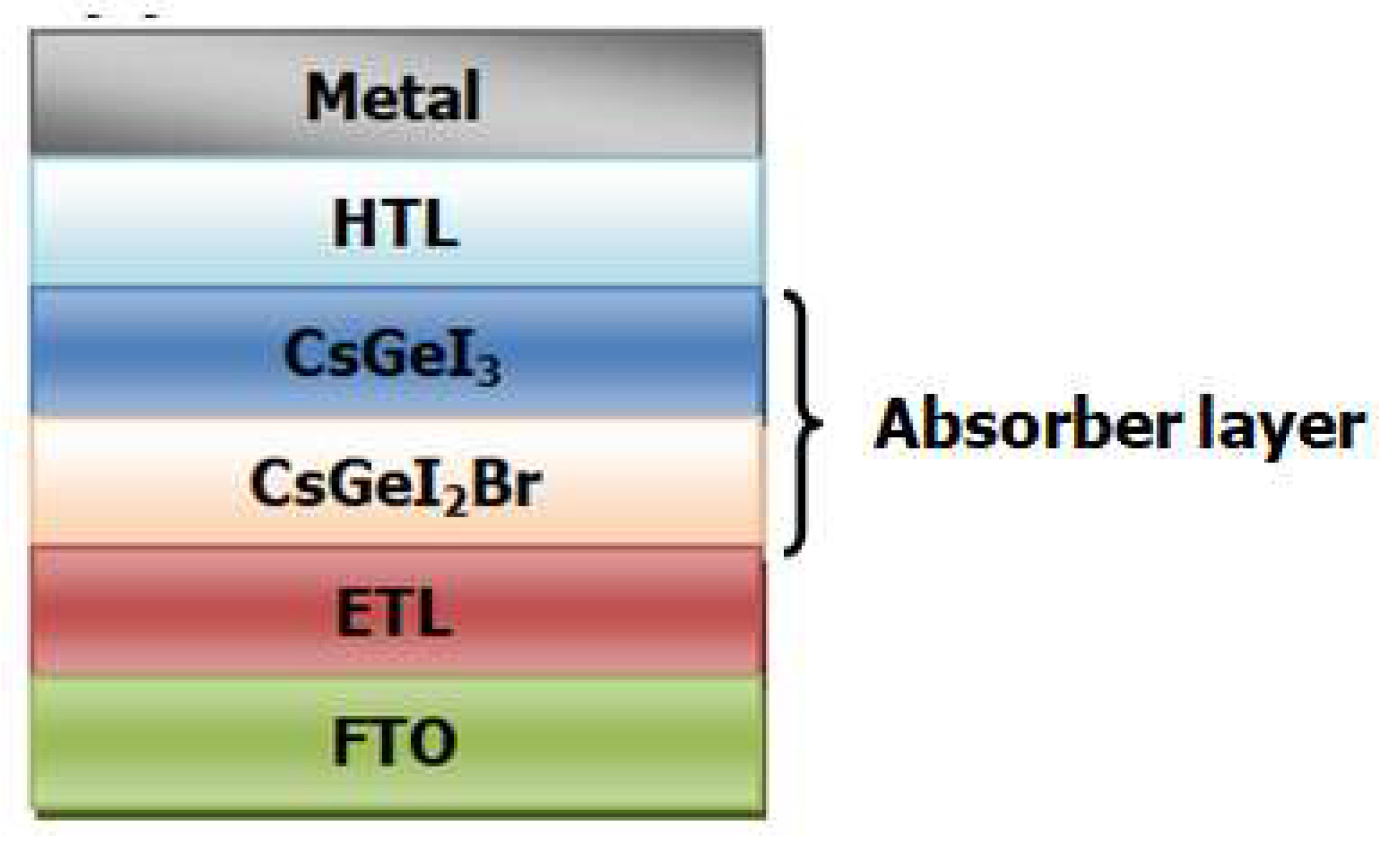
2. Materials and Methods

The solar cell structure used throughout the study, as shown in Figure 1, has six main layers. The solar cell configuration is presented as FTO/ETL/CsGeI2Br/CsGeI3/HTL/ Metal. In this system, light enters via the top FTO transparent layer. The work function of FTO is 4.1 eV. This layer is in the link between the external load and the ETL. It facilitates the extraction of electrons from the solar cell. In practice, the thickness of FTO stands between 400 to 600 nm. Within the investigations, we have chosen 400 nm. Figure 1 is simulated in SCAPS-1D with electrodes, electron and holes transport layers (ETL/HTL), and the absorber layer CsGeI2Br/CsGeI3in which the photo-generation process occurs. The FTO and ETL layers were fixed in all the simulation iterations. The metal electrodes assume the role of the link between the HTL and the external load. It facilitates the collection of holes in the external circuit due to its work function.
The heterojunction PSC was modeled in this investigation using SCAPS-1D software version 3.3.09, a device simulator created by the University of Ghent [35]. The accuracy of this simulator was already made by comparing it with real experimental devices reported by research teams [36,37]. Therefore, the SCAPS-1D is used throughout the investigations. The kernel of the SCAPS-1D platform is essentially based on three distinct coupled differential equations by numerically solving continuity and Poisson’s equations for electrons and hole charge carriers as expressed by Equations (1)–(3) [38,39].
2 φ 2 x = q ε r ε o p n + N D N A + p t n t
1 q J n x R n + G n = 0
1 q J p x R p + G p = 0
where φ defines the electrostatics potential, q represents the elementary charge, ε o represents the permittivity of free space while ε r represents the relative permittivity, p , n are, respectively, the hole and electron concentration, N D ,   N A designate, respectively, the donor and acceptor density, p t , n t define the hole and electron trapped, G p , G n stands for the generation rate of hole and electrons, respectively, R p , R n designate the recombination of hole and electrons, respectively, J p ,   J n define the density current of the electron and hole defined as Equations (4) and (5):
J n = q μ n n φ x + qD n n x
J p = q μ p p φ x qD p p x
In which μ p , μ n stands for hole and electron mobility, respectively, D p , D n define the hole and electron diffusion coefficient. In addition, the mathematical expression of the absorption coefficient used within the investigations is expressed as [35]:
α h υ = B α h υ E g
where B α designates an independent constant defined as 10 5   cm 1   eV 0.5 and h υ represents the photon energy. The input parameters for SCAPS software used throughout this work are given in Table 1.

3. Results and Discussion

This section describes the effect of thickness, the doping rate and defect of the density of the absorber layer, the thickness and the doping rate of HTL, temperature, back contact metal, shunt and series resistance on open circuit voltage V oc , short circuit current density J sc , fill factor FF and power conversion efficiency PCE . The simulations are conducted in standard test conditions wherein the irradiation is normalized at 0.1   W / cm 2 .

3.1. Optimization of the Absorber Layer

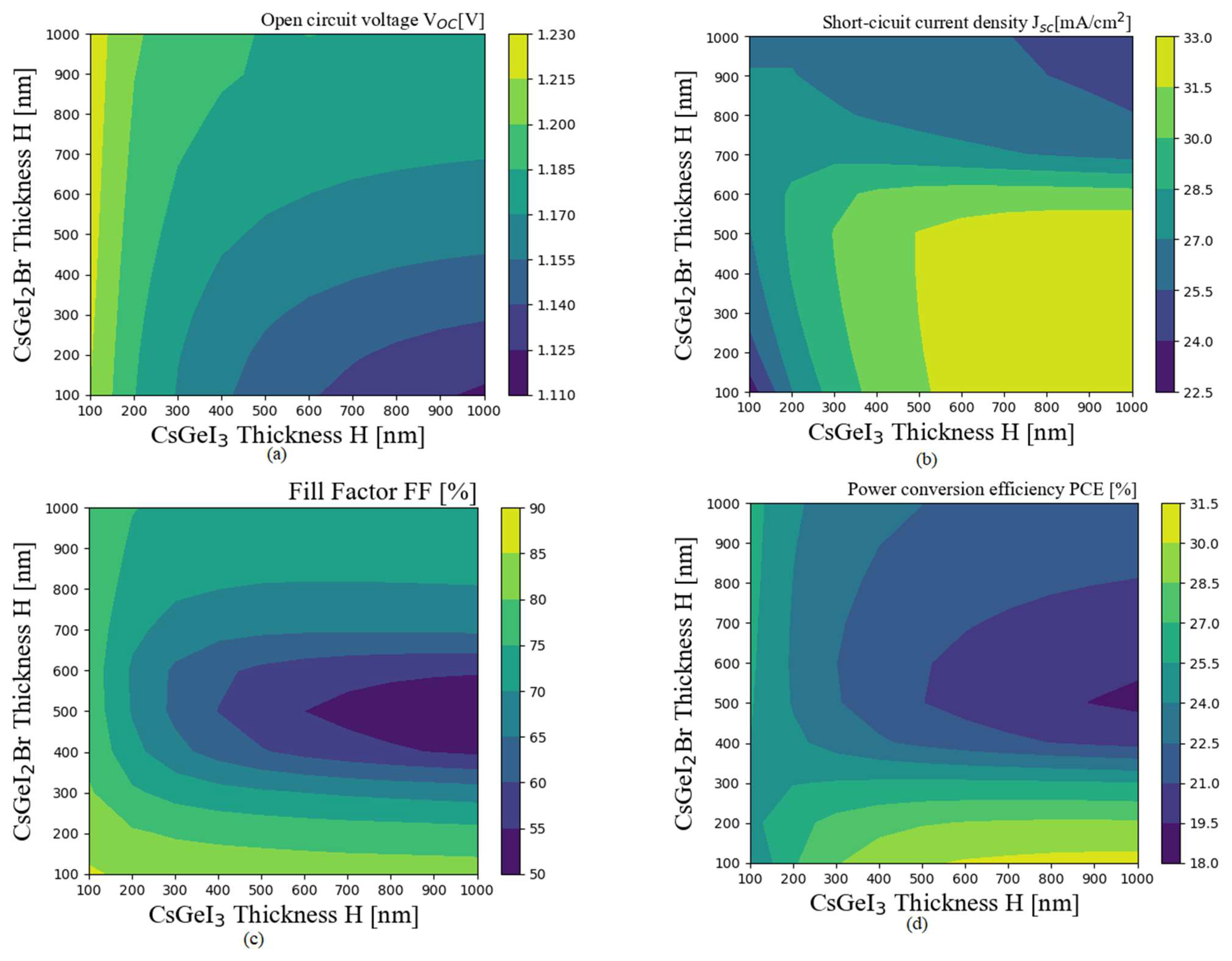
3.1.1. Impact of the Thickness of the Absorber Layer

This subsection describes the contribution of the thickness of the absorber layer on the electrical parameters, as shown in Figure 2. The thickness of the absorber layer is an important parameter while determining the performance of a solar cell. This work presents the effect of the absorber layer thicknesses on the solar cell parameters such as open circuit voltage V oc , short circuit current density J sc fill factor FF and power conversion efficiency PCE is presented here. In the simulations models used in this study, the thicknesses of absorber layers varied from 100   nm to 1000   nm . It is indicative in Figure 2 that when the thickness of the CsGeI3 is below 300   nm , there are significant increases of V oc , whereas, J sc and PCE decreases with the increases of the CsGeI2Br thickness. Moreover, Figure 2c shows that FF decreases slightly due to the V oc , J sc   and PCE results. This can be attributed to the distance that the photons have to travel through the first layer (CsGeI2Br) because of its high thickness, which acts as a barrier for the second layer (CsGeI3). Thus, the photons cannot be efficiently absorbed by CsGeI3 layer due to its low thickness. Therefore, photo-generation is unlikely to be significant in this layer, and the carriers cannot diffuse in the crystal structure to produce current. Thus, in CsGeI3 layer, the majority of the carriers photo-generated stands in the solar cell due to their low diffusion and contributes to the increase of the voltage, as shown in Figure 2a.
In contrast, when the thickness of the CsGeI2Br is less than 300   nm ,   V oc decreases while, J sc , FF , PCE increase with the thickness of the CsGeI3, as in Figure 2. Indeed, few photons are absorbed by layer CsGeI3 because of their small thickness size. This implies that the absorption of photons can be improved when the thickness of the CsGeI3 layer is large, as shown in Figure 2d. The photons can easily reach the CsGeI3 layer and contribute to the carrier’s photo-generation in this layer. This means that the amount of carrier contributing to the voltage decreases into the benefit of current as shown in Figure 2a,b because the minority carriers photo-generated are kicked out of the solar cell. This observation shows that the carriers have enough energy to leave the valence band to the conduction band and can easily be collected. Therefore, within the implementation of this prototype of PSC, the CsGeI3 layer should be thicker than the CsGeI2Br layer. In literature, the maximum efficiency of a PSC is around 33% [40,41]. This high efficiency, as shown in Figure 2d, is also due to considering the series and shunt resistance beyond the physically acceptable zone during the simulation. In addition, the limit of short circuit and open circuit voltage with respect to the band gap shows that the maximum current and voltage that can be delivered by the CsGeI3 layer 1.363   eV are 32   mA / cm 2 and 1.14   V , respectively, while the CsGeI2Br layer 1.579   eV is 28   mA / cm 2 and 1.2   V [40,41]. Thus, depending on the combination of the thicknesses of the different absorber layers, the CsGeI2Br layer can operate beyond its limits and can cause significant heating of the PSC and induce damage. Therefore, as shown in Figure 2a,b,d, the contour plots in yellow must be avoided to maintain the stability of the solar cell.

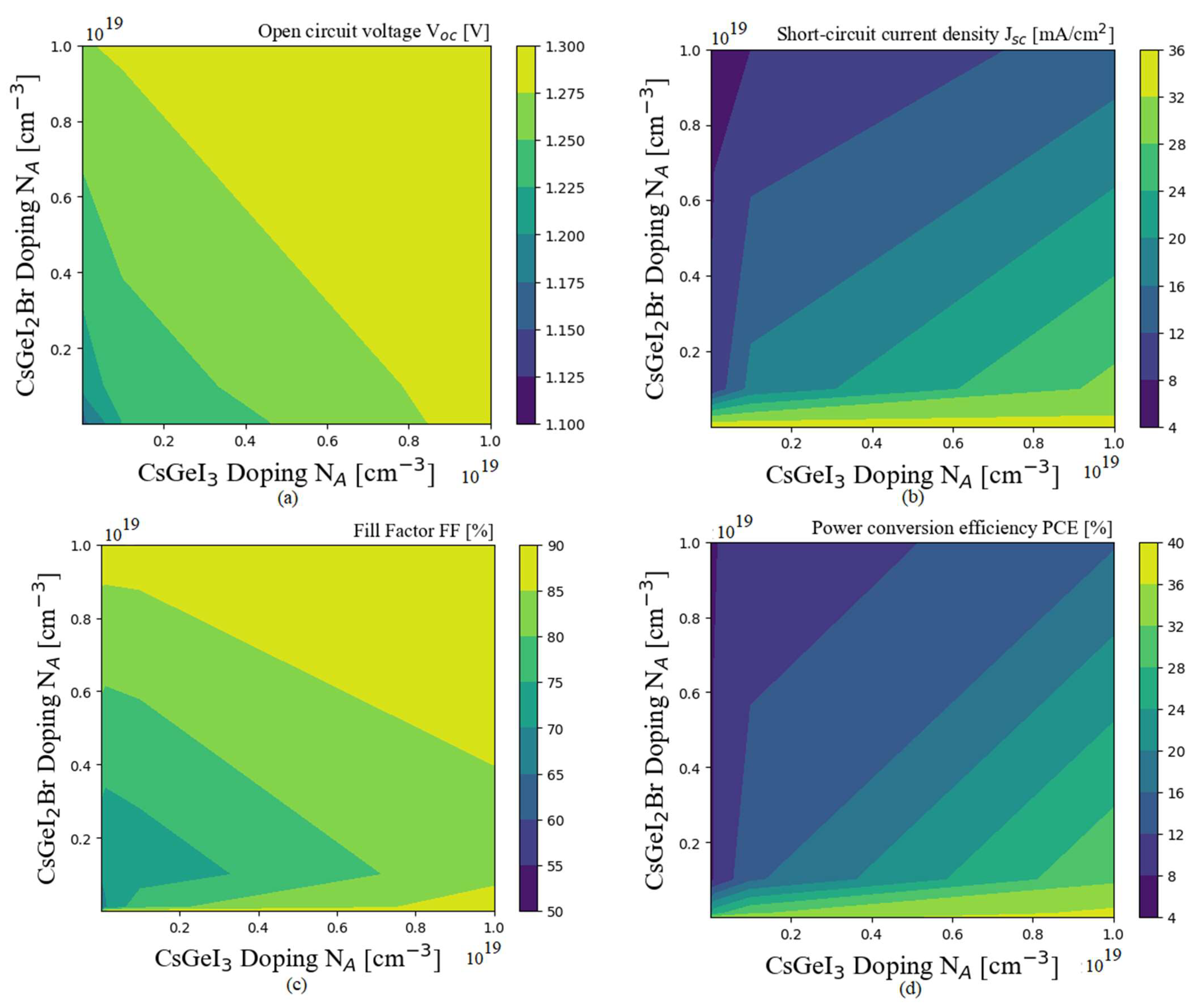
3.1.2. Impact of the Doping of the Absorber Layer

Figure 3 depicts the impact of the doping of the two absorber layers on the electrical parameters. Acceptor doping density plays a vital role in improving the performance of a PSC. In this study, the range of acceptor density of the two absorber layers was 10 14   cm 3 to 10 19   cm 3 .
We found that this PSC prototype offers high performance when the doping in the CsGeI3 layer is higher than in the CsGeI2Br layer, as shown in Figure 3d. In fact, when the doping in the CsGeI3 layer is higher than that of the CsGeI2Br layer, this favors the movement of electrons and holes in the absorber layer. This gradient of doping creates an internal electrical field in the absorber layer, and it is responsible for the significant amount of electrons emitted from the solar cell, as shown in Figure 3b, and therefore reduces the voltage, as shown in Figure 3a. However, when the doping CsGeI2Br layer is higher than that of the CsGeI3 layer, the flow of carriers is reduced, and the solar cell turns to operate as an open circuit. In this situation, the gradient of doping in the absorber layer creates an electrical field in the opposite direction to the flow of carriers in the solar cell. Thus, the carriers are photo-generated but cannot leave the solar cell and can only contribute to the increase of the voltage, as shown in Figure 3a. In the same Figure 3a, we also noted that the blocked carrier did not contribute to voltage for low doping in CsGeI3 because of the recombination process. In addition, this configuration leads to a rapid rise in temperature and can therefore damage the solar cell. Thus, within the implementation of this PSC prototype, the doping of the CsGeI3 layer should be higher than that of the CsGeI2Br layer in order to preserve the device from damage, reduce the recombination process and also improve its performance. In the literature, the maximum efficiency stands around 33% [40,41]. Thus, depending on the doping in the absorber layer, the stability of the PSC can be affected when this latter operates beyond its limits. Thus, Figure 3a,b,d show that the contour plots in yellow must be avoided to maintain the stability of the solar cell.

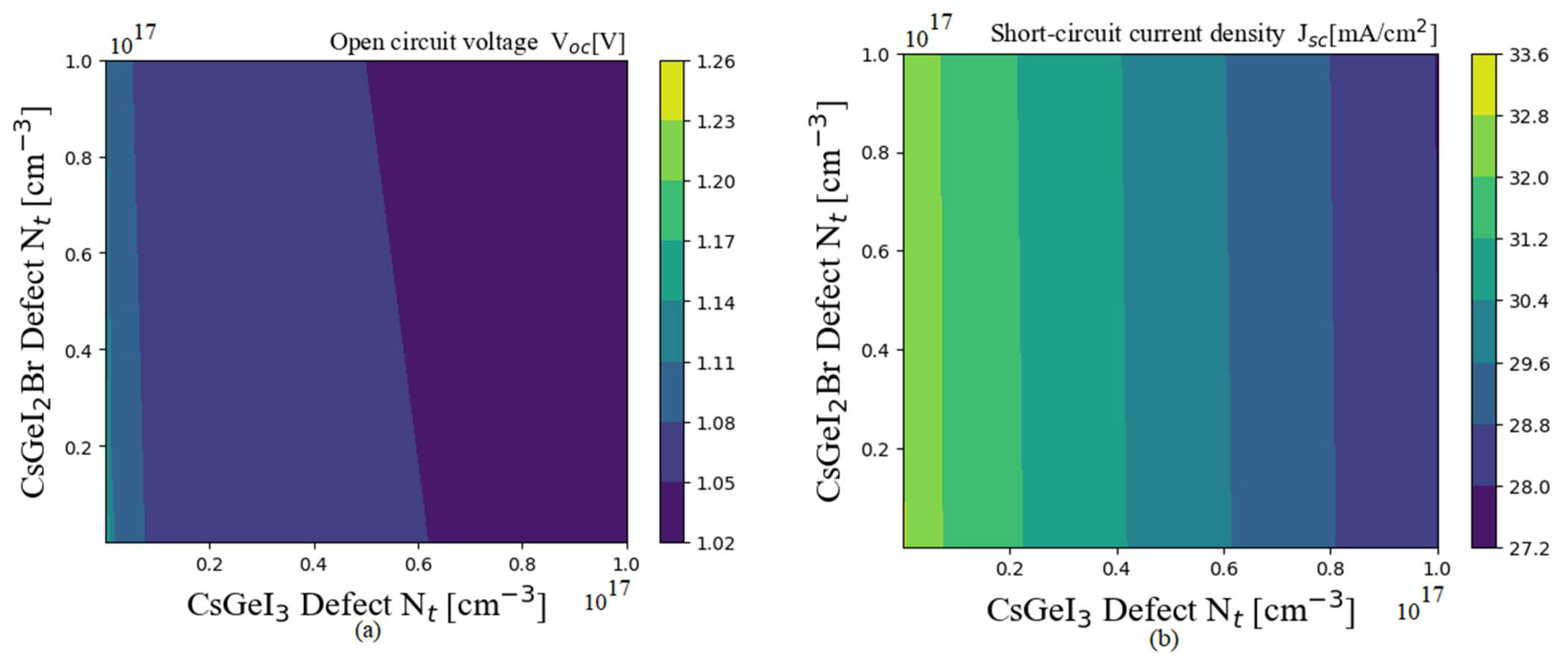
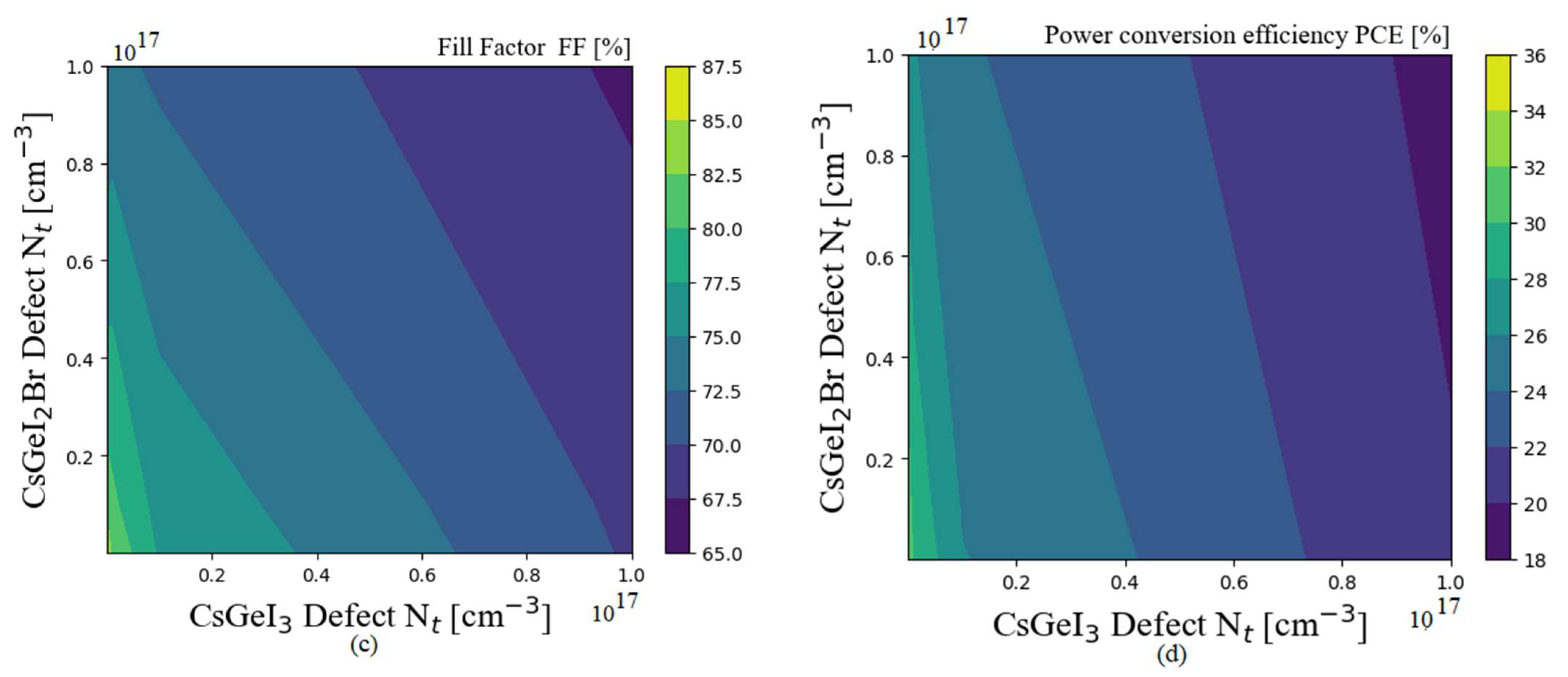
3.1.3. Impact of the Defect Densities of the Absorber Layer

The impact of the defect density (Shockley–Read–Hall) of the absorber layer on the performances of PSC is presented. Defect density influences the performance parameters of solar cells. The contribution of the defect density study is located in the absorber layers CsGeI3 and CsGeI2Br. Defect density modeling showed the imperfections in the device, leading to the carriers’ recombination. These defects are mostly created during the doping process and often during the assembly of the different layers for commercialization—there are also natural defects in the crystal structure of the material. Within the investigation, the range of defect varied was 10 13   cm 3 to 10 17   cm 3 . Figure 4 depicts the variations of electrical parameters in terms of the defect of the two absorber layers.
We reveal that the defect density of the two absorber layers affects significantly the electrical parameters, as shown in Figure 4. In fact, when the defect density increases, all the electrical parameters of this PSC decrease. The defect density is modeling the trap of carrier in a solar cell. This trap captures the carrier and favours the recombination process. Otherwise, the defect in the solar cell facilitates the collision between the carriers. This collision induces the losses of energy of the carriers during their journey in the crystal structure. Thus, they can be easily recombined due to their low energy. However, when the quantity of the trap increases, the number of carriers captured increases the recombination process and therefore, the output performance of the PSC decreases, as shown in Figure 4. This high recombination process can cause the device to heat up quickly and damage it. From the limit acceptable in terms of the current and voltage delivered by the CsGeI3 layer 1.363   eV and CsGeI2Br layer 1.579   eV [40,41], the defect density acceptable should be minimized as much as possible and is considered to be around 10 14   cm 3 to avoid the yellow areas, as shown in Figure 4a,b,d.

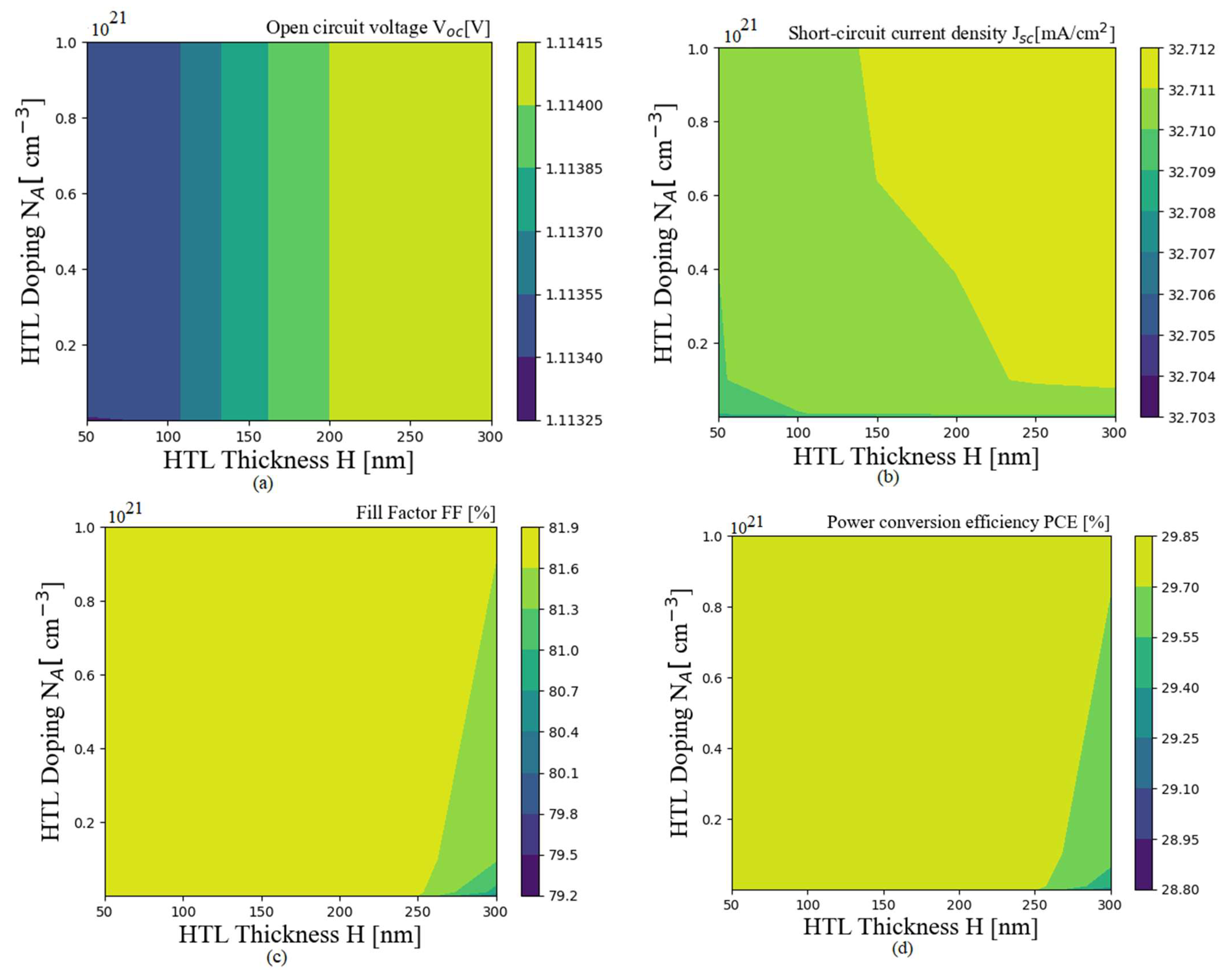
3.2. Impact of the Thickness and Doping of the HTL Layer

This section describes the impact of the hole transport layer (HTL) on the electrical parameters of the solar cells. This layer promotes the formation of holes in the device. Figure 5 depicts the contribution of thickness and doping of HTL on the electrical parameters of the PSC. The thickness varies from 50   nm to 300   nm while the doping from 10 16   cm 3 to 10 21   cm 3 .
We found that the PCE of the PSC is not affected when the thickness is less than 250   nm . In contrast, beyond 250   nm , PCE starts to be affected for low doping and recapture when the doping is high. These results show that P3HT can easily promote the hole when the doping is subsequently high, and the thickness of the HTL is less than 250 nm. Viewing the low variation of the parameters, as shown in Figure 5, we notice that P3HT does not really affect the performance of the solar cell. Thus, during the manufacturing of this new prototype, the thickness of P3HT should be very low as possible, around 50 nm, because of its high cost as it has almost no effect on the dynamics of the solar cell.

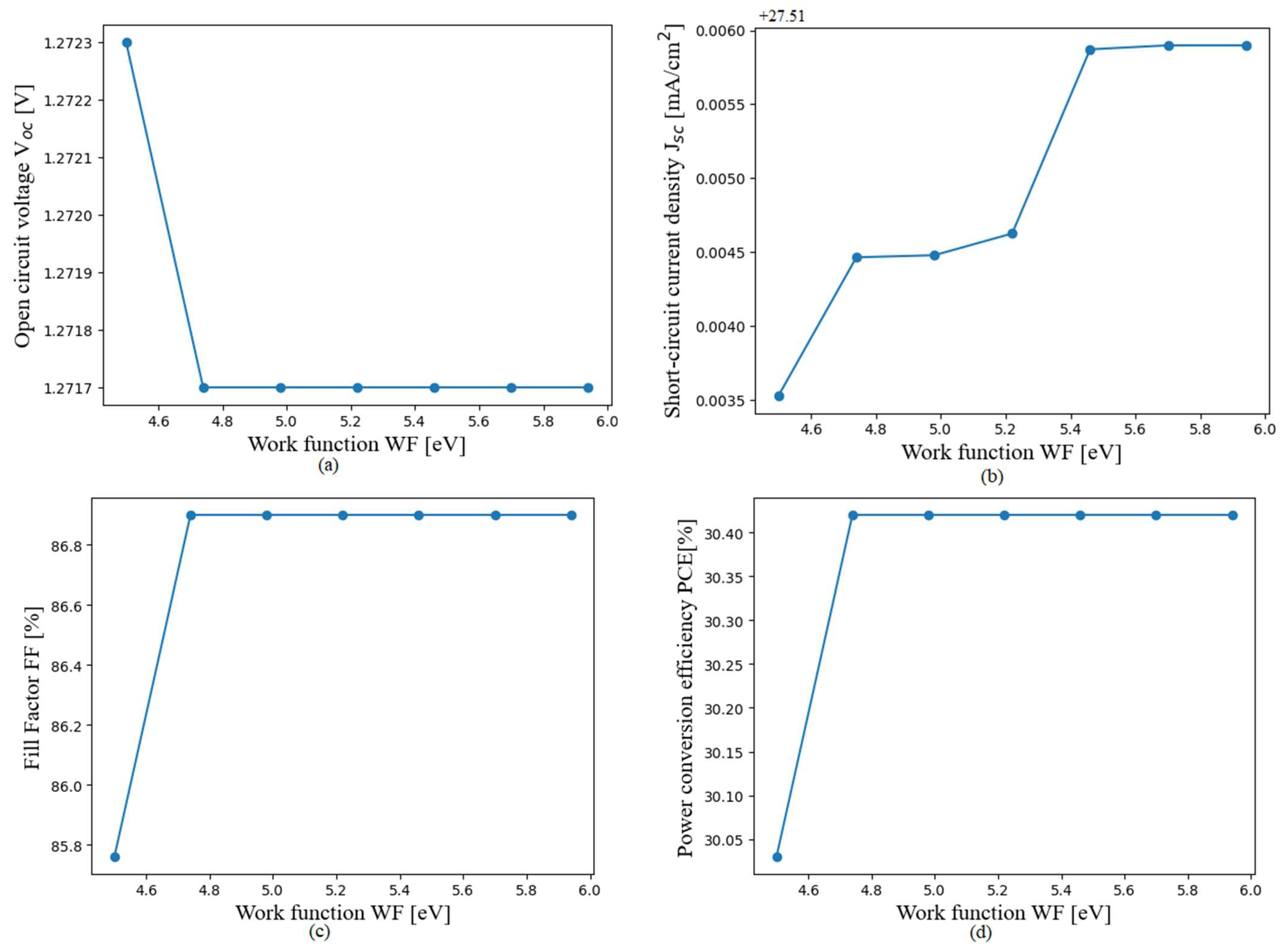
3.3. Impact of the Back Contact Metal

This subsection focuses on the impact of the back contact metal on the performance of the new prototype PSC. The back contact metal also contributes to the enhancement of the efficiency of a solar cell. Figure 6 shows the impact of the work function of the back contact metal on the electrical parameters. In our simulation, we varied the work function from 4.8   eV to 6   eV , as shown in Figure 6.
We notice that the efficiency increases with the increase in work function and remained almost constant after 5   eV . In addition, we revealed a very low variation of the electrical parameters. Thus, in order to realize better performance of this prototype of PSC, it is essential to choose an appropriate metal electrode having a work function of at least equal to 5   eV .

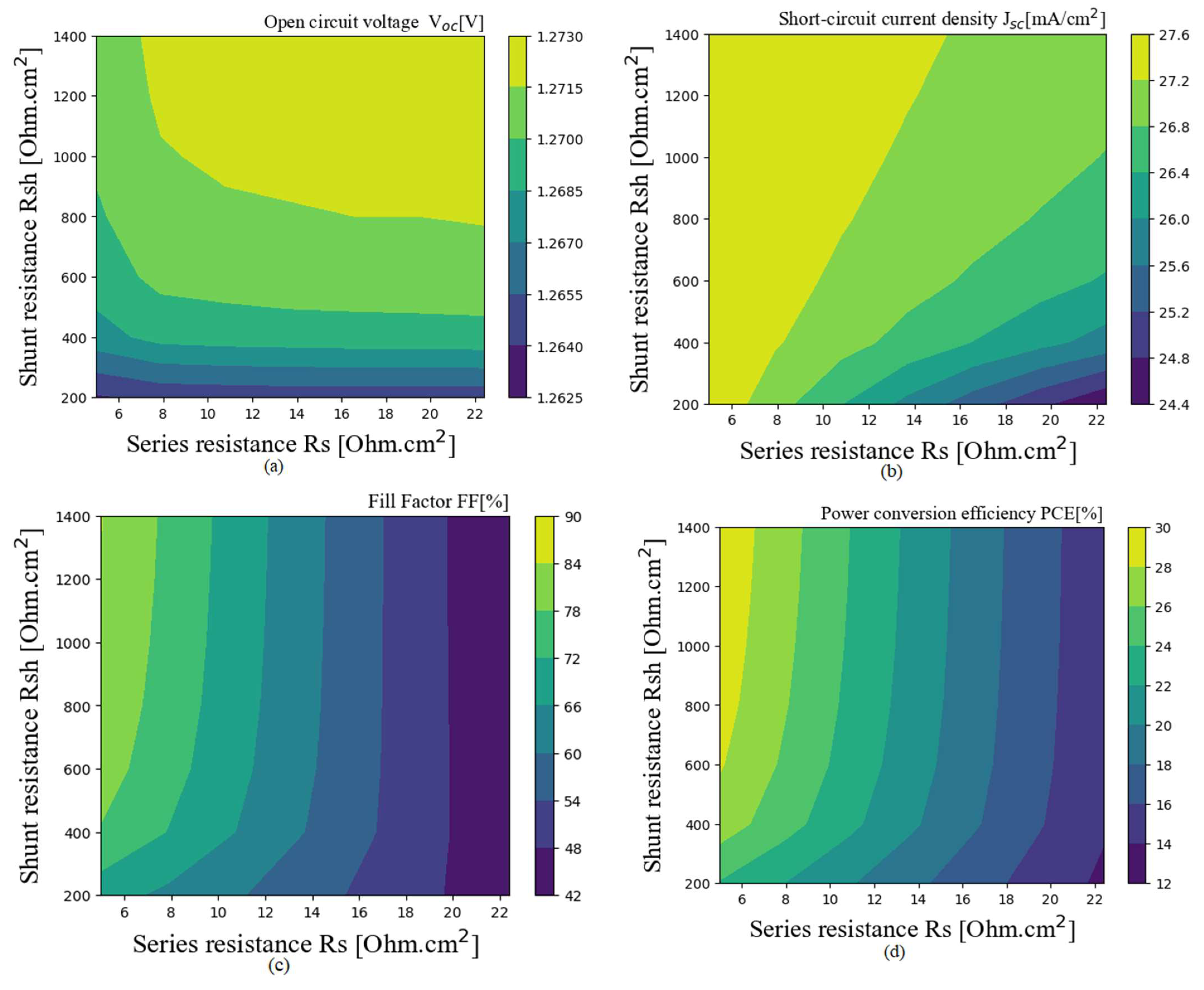
3.4. Impact of the Shunt and Series Resistances

Figure 7 depicts the contribution of series and shunt resistance on the performance of solar cell parameters. Series resistance modeling shows the electrical defect of the device due to the front and back contact of the device with the external load, while shunt resistance modeling shows the leakage current at the edge of the solar cell. The series R s and shunt resistance R sh were varied in the ranges 5 25   Ω cm 2 and 200 1400   Ω cm 2 , respectively.
We reveal that the series and shunt resistance significantly affect the PCE, as shown in Figure 7d. The open circuit voltage, as shown in Figure 7a, is more related to the lower values of shunt resistance than series resistance. However, the short circuit current is more sensitive to the high values of series resistance than shunt resistance. The fill factor is also strongly dependent on the change in series resistance, as shown in Figure 7c. From these observations, we note that the device offers a high PCE when the leakage current is low (high shunt resistance) and the series resistance is low so that the carrier can be collected by the metal electrode.

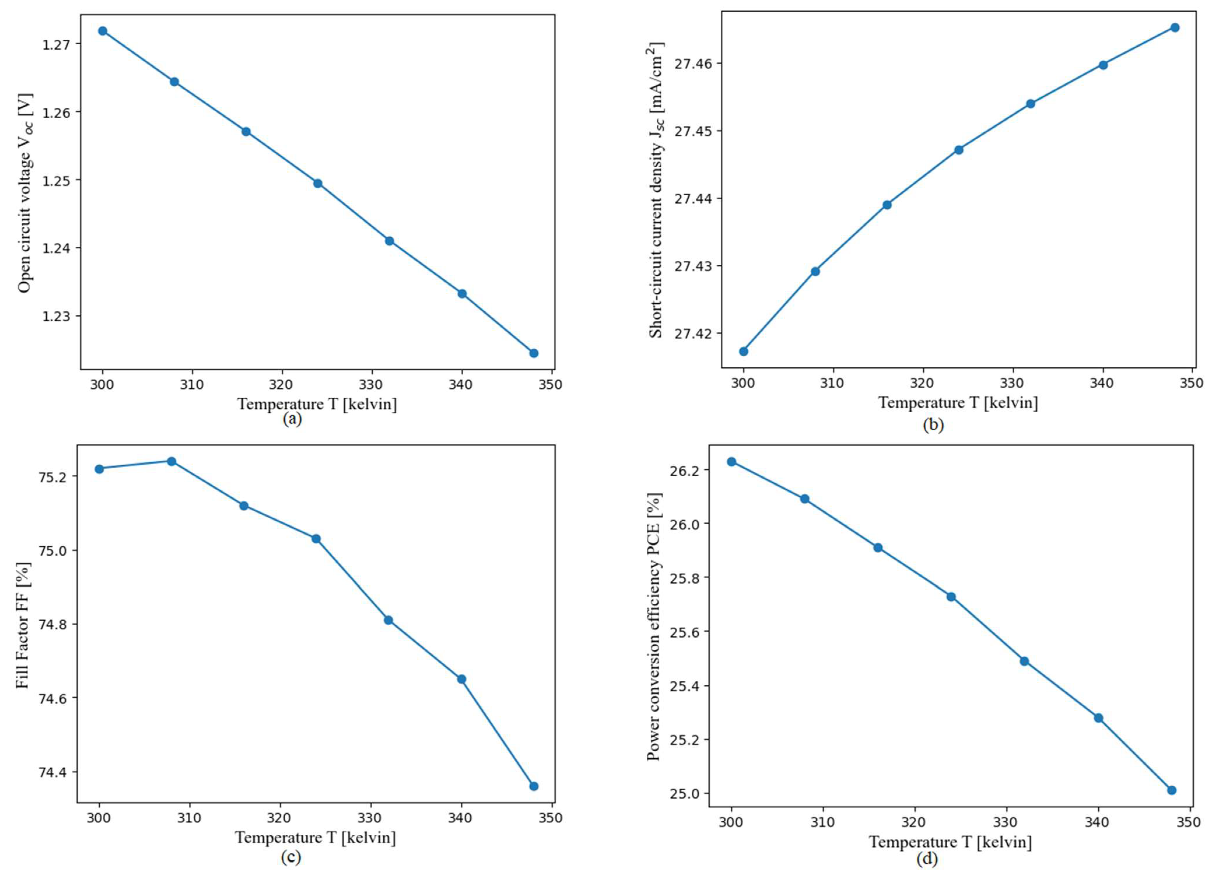
3.5. Impact of the Temperature

Temperature is the main parameter that causes damage to the PSC. The rise in the solar temperature is due to the amount of irradiation transformed into heat. Figure 8 presents the impact of temperature on PSC and the electrical parameters. The range of temperature varied from 300 350   Kelvin .
From the results shown in Figure 8, we note that when the temperature increases, J sc increases while the FF , V oc and PCE decrease. Indeed, the temperature favours the thermal agitation of carriers in the solar cell. Thus, this thermal agitation induced very little additional extraction of the carriers out of the solar cell traduce by a mild increase in current, as shown in Figure 8b. Thus, this extraction reduced the population of carriers in the solar cell and reduced the voltage, as shown in Figure 8a. The variations in the current and voltage reduced the FF and, therefore, the PCE of the solar cell. Table 2 and Table 3 show the best solar cell structure and performance.
In addition, the temperature rise of the device can also be due to one of the absorber layers of the device operating beyond its limits. Indeed, this layer also operates as an ohmic conductor and significantly reduces the flow of carriers in the solar cell. The concerned layer will transform the electrical energy into heat through the Joule effect, and increase the temperature of the device. In addition, given the confinement of the different parts of a PSC, the temperature of the device can quickly rise and can cause damage. So, to fabricate this specific heterojunction solar cell, the boundaries of each absorber layer must be considered.
The performance of the heterojunction PSC as shown in Table 3 will be very difficult to achieve during experimentation due to the maximum current ( 32.79   mA / cm 2 )   that is slightly greater than 28   mA / cm 2 (CsGeI2Br layer) [40,41]. Thus, under these operating conditions, this prototype will become lightly hot and its performance in real-life conditions will decrease because of this rise in temperature.

4. Conclusions

The aim of this paper was to simulate a lead-free heterojunction perovskite solar cell (PSC) made of CsGeI2Br/CsGeI3 using SCAPS-1D software. The simulation of this new prototype of PSC starts with the design of the absorber layer made of two perovskite materials CsGeI2Br/CsGeI3, the TiO2 as electron transport layer (ETL) and P3HT (poly(3-hexylthiophene) as hole transport layer (HTL) withSCAPS-1D software. The impact of the thicknesses, doping and defect density of the absorber layer is checked, followed by the contribution of thickness and the doping of the HTL. The simulations were also conducted on the effect of the back contact metal, temperature, shunt and series resistance on the electrical parameters of this new prototype. The simulations were conducted in standard test conditions (STC) using the SCAPS-1D platform. We found that the new prototype offers a maximum simulated efficiency of 31.86 % when the CsGeI3 thickness should be around 900   nm while the CsGeI2Br thickness should be around 100   nm . CsGeI3 doping should be around 10 18   cm 3 and CsGeI2Br doping around 10 16   cm 3 . Defect density in both layers of the absorber should be around 10 14   cm 3 . We also notice that the P3HT and the back contact metal do not significantly affect the performance of this novel type of heterojunction PSC. Thus, within the manufacturing of this specific PSC, only the absorber layer, FTO and ETL can be considered in order to check the stability and efficiency of this prototype. Furthermore, the temperature of the new PSC should be maintained around 25 °C. In terms of future research, an experimental investigation must be done to check the stability and lifetime of this new device under weather conditions in real time. Additionally, the contributions of different HTL, ETL and FTO on the dynamics of this prototype should be investigated.

Author Contributions

Conceptualization, A.D.K.K. and M.M.; methodology, A.D.K.K.; software, A.D.K.K.; validation, A.D.K.K., M.M. and N.M.T.; formal analysis, A.D.K.K.; investigation, A.D.K.K.; resources, A.D.K.K.; data curation, A.D.K.K. and N.M.T.; writing—original draft preparation, A.D.K.K., M.M. and N.M.T.; writing—review and editing, A.D.K.K. and M.M.; visualization, A.D.K.K.; supervision, A.D.K.K.; project administration, M.M.; funding acquisition, M.M. All authors have read and agreed to the published version of the manuscript.

Funding

This research was funded by Tshwane University of Technology PV Nanocomposites R&D Platform and iThemba LABS of the National Research Foundation of South Africa.

Institutional Review Board Statement

Not applicable.

Informed Consent Statement

Not applicable.

Data Availability Statement

Not applicable.

Acknowledgments

The authors gratefully acknowledge financial and material support from the Tshwane University of Technology PV Nanocomposites R&D Platform and iThemba LABS of the National Research Foundation of South Africa.

Conflicts of Interest

The authors declare no conflict of interest.

References

  1. Kapim, A.D.; Nangmetio, C.A.; Kuatche, N.J. Computational improvement of the performance of thermoelectric element (Generator and Cooler) using an external magnetic field. J. Electron. Mater. 2023, 52, 951–959. [Google Scholar] [CrossRef]
  2. Kumar, A.; Khan, M.Z.U.; Pandey, B. Wind Energy: A Review Paper. Gyancity J. Eng. Technol. 2018, 4, 29–37. [Google Scholar] [CrossRef]
  3. Pelap, F.B.; Konga, E.T.; Kapim, K.A.D. Numerical Optimization of a Tandem Solar Cell based on InxGa1-xN. J. Ren. Energy 2021, 24, 25–39. [Google Scholar] [CrossRef]
  4. Kapim, K.A.D.; Konga, E.; Pelap, F.B. Contribution of a non-uniform magnetic field on the electric power of a photovoltaic panel. J. Energy Technol. Policy 2020, 10, 16–29. [Google Scholar] [CrossRef]
  5. Li, C.; Wang, Y.; Choy, W.C. Efficient interconnection in perovskite tandem solar cells. Small Methods 2020, 4, 2000093. [Google Scholar] [CrossRef]
  6. Han, Q.; Bae, S.H.; Sun, P.; Hsieh, Y.T.; Yang, Y.M.; Rim, Y.S.; Zhao, H.; Chen, Q.; Shi, W.; Li, G.; et al. Single crystal formamidinium lead iodide (FAPbI3): Insight into the structural, Optical and Electrical Properties. Adv. Mater. 2016, 28, 2253–2258. [Google Scholar] [CrossRef]
  7. Mu, C.; Pan, J.; Feng, S.; Li, Q.; Xu, D. Quantitative doping of chlorine in formamidinium lead trihalide (FAPbI3-xClx) for planar hetero-junction perovskite solar cells. Adv. Energy Mater. 2017, 7, 1601297. [Google Scholar] [CrossRef]
  8. Wei, Q.; Zi, W.; Yang, Z.; Yang, D. Photoelectric performance and stability comparison of MAPbI3 and FAPbI3 perovskite solar cells. Sol. Energy 2018, 174, 933–939. [Google Scholar] [CrossRef]
  9. Zhang, Y.; Grancini, G.; Feng, Y.; Asiri, A.M.; Nazeeruddin, M.K. Optimization of table quasi-cubic FAxMA1–xPbI3 perovskite structure for solar cells with efficiency beyond 20%. ACS Energy Lett. 2017, 2, 802–806. [Google Scholar] [CrossRef]
  10. Ahmed, A.; Riaz, K.; Mehmood, H.; Tauqeer, T.; Ahmad, Z. Performance optimization of CH3NH3Pb(I1-xBrx)3 based perovskite solar cells by comparing diferent ETL materials through conduction band offset engineering. Opt. Mater. 2021, 105, 109897. [Google Scholar] [CrossRef]
  11. Karimi, E.; Ghorashi, S. The efect of SnO2 and ZnO on the performance of perovskite solar cells. J. Electron. Mater. 2020, 49, 364–376. [Google Scholar] [CrossRef]
  12. Chowdhury, T.H.; Ferdaous, M.T.; Wadi, M.A.A.; Chelvanathan, P.; Amin, N.; Islam, A.; Kamaruddin, N.; Zin, M.I.M.; Ruslan, M.H.; Sopian, K.B.; et al. Prospects of ternary Cd1−xZnxS as an electron transport layer and associated interface defects in a planar lead halide perovskite solar cell via numerical simulation. J. Electron. Mater. 2018, 47, 3051–3058. [Google Scholar] [CrossRef]
  13. Jiang, Q.; Zhang, X.; You, J. SnO2: A wonderful electron transport layer for perovskite solar cells. Small 2018, 14, 1801154. [Google Scholar]
  14. Rai, N.; Rai, S.; Singh, P.K.; Dwivedi, D.K. Analysis of various ETL materials for an effcient perovskite solar cell by numerical simulation. J. Mater. Sci. Mater. Electron. 2020, 31, 16269–16280. [Google Scholar] [CrossRef]
  15. Shasti, M.; Mortezaali, A. Numerical study of Cu2O, SrCu2O2, and CuAlO2 as hole transport materials for application in perovskite solar cells. Phys. Status Solidi A 2019, 216, 1900337. [Google Scholar] [CrossRef]
  16. Rossi, F.D.; Renno, G.; Taheri, B.; Nila, N.Y.; Illieva, V.; Fin, A.; Carlo, A.D.; Bonomo, M.; Barolo, C.; Brunetti, F. Modifed P3HT materials as hole transport layers for fexible perovskite solar cells. J. Power Sources 2021, 494, 229735. [Google Scholar] [CrossRef]
  17. Li, S.; Cao, Y.L.; Li, W.H.; Bo, Z.S. A brief review of hole transporting materials commonly used in perovskite solar cells. Rare Met. 2021, 40, 2712–2729. [Google Scholar] [CrossRef]
  18. Momblona, C.; Malinkiewicz, O.; Carmona, C.R.; Soriano, A.; Escrig, L.G.; Bandiello, E.; Scheepers, M.; Edri, E.; Bolink, H.J. Efficient methylammonium lead iodide perovskite solar cells with active layers from 300 to 900 nm. APL Mater. 2014, 2, 081504. [Google Scholar] [CrossRef] [Green Version]
  19. Wang, G.T.; Wei, J.H.; Peng, Y.F. Electronic and optical properties of mixed perovskites CsSnxPb(1−x)I3. AIP Adv. 2016, 6, 065213. [Google Scholar] [CrossRef] [Green Version]
  20. Manspeaker, C.; Zakhidov, A. Predicting hybrid perovskite performance based on secondary cation choice. Sol. Energy 2022, 241, 686–692. [Google Scholar] [CrossRef]
  21. Mahapatra, B.; Krishna, R.V.; Laxmi; Patel, P.K. Design and optimization of CuSCN/CH3NH3PbI3/TiO2 perovskite solar cell for efficient performance. Opt. Commun. 2022, 504, 127496. [Google Scholar] [CrossRef]
  22. Ritu; Gagandeep; Kumar, R.; Chand, F. Performance enhancement in MA0.7FA0.3PbI3 based perovskite solar cell by gradient doping. Optik 2023, 274, 170558. [Google Scholar] [CrossRef]
  23. Ahmed, T.; Shamima, S.U.D.; Maity, S.K.; Basak, A. Performance evaluation of lead free CH3NH3SnI3/GeTe Tandem solar cell with HTL layer by SCAPS 1D. Optik 2023, 282, 170836. [Google Scholar] [CrossRef]
  24. Akhtarianfar, S.F.; Shojaei, S.; Asl, S.K. High-performance CsPbI3/XPbI3 (X=MA and FA) heterojunction perovskite solar cell. Opt. Commun. 2022, 512, 128053. [Google Scholar] [CrossRef]
  25. Mukaddar, S.k.; Ghosh, S. 16.35% efficient Cs2GeSnCl6 based heterojunction solar cell with hole-blocking SnO2 layer: DFT and SCAPS-1D simulation. Optik 2022, 267, 169608. [Google Scholar] [CrossRef]
  26. Gourav; Ramachandran, K. Understanding the electronic, structural, optical, photovoltaic and thermoelectric properties of Cs2GeSnBr6 by first-principles and SCAPS-1D simulation. Optik 2023, 282, 170822. [Google Scholar] [CrossRef]
  27. Khatoon, S.; Yadav, S.K.; Chakraborty, V.; Singh, J.; Singh, R.B. A simulation study of all inorganic lead-free CsSnBr3 tin halide perovskite solar cell. Mater. Today Proc. 2023, in press. [Google Scholar] [CrossRef]
  28. Kumar, M.; Raj, A.; Kumar, A.; Anshu, A. Effect of band-gap tuning on lead-free double perovskite heterostructure devices for photovoltaic applications via SCAPS simulation. Mater. Today Commun. 2021, 26, 101851. [Google Scholar] [CrossRef]
  29. Sarkar, J.; Talukdar, A.; Debnath, P.; Chatterjee, S. Study of bromine substitution on band gap broadening with consequent blue shift in optical properties and efficiency optimization of lead-free CsGeIxBr3−x based perovskite solar cells. J. Comput. Electron. 2023, 22, 1075–1088. [Google Scholar] [CrossRef]
  30. Miah, M.H.; Rahman, M.B.; Mayeen, F.K.; Khandaker, U.; Hatta, S.F.W.M.; Soin, N.B.; Islam, M.A. Optimization and detail analysis of novel structure Pb-free CsGeI3-based all-inorganic perovskite solar cells by SCAPS-1D. Optik 2023, 281, 170819. [Google Scholar] [CrossRef]
  31. Saikia, D.; Bera, J.; Betal, A.; Sahu, S. Performance evaluation of an all inorganic CsGeI3 based perovskite solar cell by numerical simulation. Opt. Mater. 2022, 123, 111839. [Google Scholar] [CrossRef]
  32. Das, A.; Samajdar, D.P. Simulation of CsGeI3-based perovskite solar cells using graphene Oxide interfacial layer for improved device performance. In Proceedings of the International Conference and Emerging Electronics, Bangalore, India, 11–14 December 2022. [Google Scholar]
  33. Ahmad, W.; Noman, M.; Jan, S.T.; Khan, A.D. Performance analysis and optimization of inverted inorganic CsGeI3 perovskite cells with carbon/cupper charge transport materials using SCAPS-1D. R. Soc. Open. Sci. 2023, 10, 221127. [Google Scholar] [CrossRef]
  34. Tulka, T.K.; Alam, N.; Akhtaruzzaman, M.; Sobayel, K.; Hossain, M.M. Optimization of a high-performance lead-free cesium-based inorganic perovskite solar cell through numerical approach. Heliyon 2022, 8, e11719. [Google Scholar] [CrossRef]
  35. Burgelman, M.; Nollet, P.; Degrave, S. Modelling polycrystalline semiconductor solar cells. Thin Solid Films 2000, 361, 527–532. [Google Scholar] [CrossRef]
  36. Liu, D.; Kelly, T.L. Perovskite solar cells with a planar hetero-junction structure prepared using room-temperature solution processing techniques. Nat. Photonics 2014, 8, 133–138. [Google Scholar] [CrossRef]
  37. Karthick, S.; Velumani, S.; Bouclé, J. Experimental and SCAPS simulated formamidinium perovskite solar cells: A comparison of device performance. Sol. Energy 2020, 205, 349–357. [Google Scholar] [CrossRef]
  38. Hossain, M.K.; Toki, G.F.I.; Alam, I.; Pandey, R.; Samajdar, D.P.; Rahman, M.F.; Islam, M.R.; Rubel, M.H.K.; Bencherif, H.; Madane, J.; et al. Numerical simulation and optimization of aCsPbI3-based perovskite solar cell to enhance the power conversion efficiency. N. J. Chem. 2023, 47, 4801–4817. [Google Scholar] [CrossRef]
  39. Sharma, D.; Mehra, R.; Balwinder, R. Mathematical modelling and simulation of CH3NH3Pb(I1−xBrx)3-based perovskite solar cells for high efficiency. J. Comput. Electron. 2023, 22, 383–393. [Google Scholar] [CrossRef]
  40. Baena, J.P.C.; Saliba, M.; Buonassisi, T.; Grätzel, M.; Abate, A.; Tress, W.; Hagfeldt, A. Promises and challenges of perovskite solar cells. Science 2017, 358, 739–744. [Google Scholar] [CrossRef] [Green Version]
  41. Unger, E.L.; Kegelmann, L.; Suchan, K.; Sorell, D.; Korte, L.; Albrecht, S. Roadmap and roadblocks for the band gap tunability of metal halide perovskites. J. Mater. Chem. A 2017, 5, 11401–11409. [Google Scholar] [CrossRef]
Figure 1. Presentation of the CsGeI2Br/CsGeI3 perovskite heterojunction solar cell.
Solar 03 00025 g001
Figure 2. Contribution of the thicknesses of the absorber layer on the electrical properties of PSC with the system parameters: (a) open circuit voltage V oc , (b) short circuit current J sc , (c) fill factor FF, and (d) power conversion efficiency PCE.
Solar 03 00025 g002
Figure 3. Effect of doping CsGeI3 and CsGeI2Br absorber layers on electrical performance parameters with the system parameters: N t CsGeI 2 Br = 10 14   cm 3 , N t CsGeI 3 = 10 14   cm 3 , H CsGeI 2 Br = 100   nm , H CsGeI 3 = 900   nm (a) open circuit voltage V oc , (b) short circuit current J sc , (c) fill factor FF, and (d) power conversion efficiency PCE.
Solar 03 00025 g003
Figure 4. Contribution of defect density CsGeI3 and CsGeI2Br absorber layer on the electrical quantities with the system parameters: N A CsGeI 2 Br = 10 16   cm 3 , N A CsGeI 3 = 10 17   cm 3 , H CsGeI 2 Br = 100   nm ,   H CsGeI 3 = 900   nm . (a) open circuit voltage V oc , (b) short circuit current J sc , (c) fill factor FF, and (d) power conversion efficiency PCE.
Solar 03 00025 g004aSolar 03 00025 g004b
Figure 5. Contribution of doping and thickness of the HTL on the electrical quantities with the system parameters: N t CsGeI 2 Br = 10 14   cm 3 , N t CsGeI 3 = 10 14   cm 3 , N A CsGeI 2 Br = 10 16   cm 3 , N A CsGeI 3 = 10 17   cm 3 , H CsGeI 2 Br = 100   nm , H CsGeI 3 = 900   nm . (a) open circuit voltage V oc , (b) short circuit current J sc , (c) fill factor FF, and (d) power conversion efficiency PCE.
Solar 03 00025 g005
Figure 6. Impact of work function on the electrical quantities with the system parameters: N A CsGeI 2 Br = 10 16   cm 3 , N A CsGeI 3 = 10 18   cm 3 , H CsGeI 2 Br = 900   nm , H CsGeI 3 = 100   nm . (a) open circuit voltage V oc , (b) short circuit current J sc , (c) fill factor FF, and (d) power conversion efficiency PCE.
Solar 03 00025 g006
Figure 7. Effect of the series and shunt resistance on the electrical quantities with the system parameters: N A CsGeI 2 Br = 10 16   cm 3 , N A CsGeI 3 = 10 18   cm 3 , N t CsGeI 2 Br = 10 14   cm 3 , N t CsGeI 3 = 10 14   cm 3 ,   H CsGeI 2 Br = 900   nm ,   H CsGeI 3 = 100   nm . (a) open circuit voltage V oc , (b) short circuit current J sc , (c) fill factor FF, and (d) power conversion efficiency PCE.
Solar 03 00025 g007
Figure 8. Impact of the temperature on the electrical quantities with the system parameters: N A CsGeI 2 Br = 10 16   cm 3 , N A CsGeI 3 = 10 18   cm 3 , H CsGeI 2 Br = 100   nm , H CsGeI 3 = 900   nm   R s = 5   Ω cm 2   R s h = 1200   Ω cm 2 . (a) open circuit voltage V oc , (b) short circuit current J sc , (c) fill factor FF, and (d) power conversion efficiency PCE.
Solar 03 00025 g008
Table 1. Properties of each layer.
ParametersFTO [22]ETL [24]CsGeI3 [29]CsGeI2Br [29]P3HT [39]
H (nm)40025400 *400 *150 *
Eg (eV)3.53.251.3631.5791.7
χ (eV)4.14.083.763.763.5
εr9918183
Nc (1/cm3)2 × 10182 × 10211.56 × 10179.65 × 10172.2 × 1018
Nv (1/cm3)1.8 × 10191.8 × 10202.86 × 10181.04 × 10182.2 × 1018
μn(cm2/Vs)202020201.8 × 10−3
μp(cm2/Vs)101020201.8 × 10−2
ND (1/cm3)10201018000
NA (1/cm3)001016 *1016 *1018 *
Vt (cm/s)107107107107107
Nt (1/cm3)101410141014 *1014 *1014
* Varied.
Table 2. Best properties of each layer.
ParametersFTOETLCsGeI3CsGeI2BrP3HT
H (nm)4002590010050
Eg (eV)3.53.251.3631.5791.7
χ (eV)4.14.083.763.763.5
εr9918183
Nc (1/cm3)2 × 10182 × 10211.56 × 10179.65 × 10172.2 × 1018
Nv (1/cm3)1.8 × 10181.8 × 10202.86 × 10181.04 × 10182.2 × 1018
μn (cm2/Vs)202020201.8 × 10−3
μp (cm2/Vs)101020201.8 × 10−2
ND (1/cm3)10201018000
NA (1/cm3)00101810161018
Vt (cm/s)107107107107107
Nt (1/cm3)10141014101410141014
Table 3. Performance of the new device.
Device StructureFF (%)PCE (%)Voc (V)Jsc (mA/cm2)
FTO/TiO2/CsGeI2Br/CsGeI3/P3HT/Au79.1931.861.226832.79
Disclaimer/Publisher’s Note: The statements, opinions and data contained in all publications are solely those of the individual author(s) and contributor(s) and not of MDPI and/or the editor(s). MDPI and/or the editor(s) disclaim responsibility for any injury to people or property resulting from any ideas, methods, instructions or products referred to in the content.

