Article

Cu-Doped Sb2Se3 Thin-Film Solar Cells Based on Hybrid Pulsed Electron Deposition/Radio Frequency Magnetron Sputtering Growth Techniques

1
Campus Duque de Caxias, Universidade Federal do Rio de Janeiro, Rio de Janeiro 25240-005, Brazil
2
Consiglio Nazionale delle Ricerche, IMEM Institute, 43124 Parma, Italy
3
Department of Mathematical, Physical and Computer Sciences, University of Parma, Parco Area delle Scienze 7/a (Campus), 43124 Parma, Italy
4
Department of Chemistry, Life Sciences and Environmental Sustainability, University of Parma, Parco Area delle Scienze 15/a (Campus), 43124 Parma, Italy
5
Centre d′Excellence Régional pour la Maîtrise de l′Electricité (CERME), University of Lomé, Lomé 01 BP 1515, Togo
*
Authors to whom correspondence should be addressed.
Solar 2024, 4(1), 83-98; https://doi.org/10.3390/solar4010004
Submission received: 7 December 2023 / Revised: 15 January 2024 / Accepted: 30 January 2024 / Published: 4 February 2024

Abstract

:
In recent years, research attention has increasingly focused on thin-film photovoltaics utilizing Sb2Se3 as an ideal absorber layer. This compound is favored due to its abundance, non-toxic nature, long-term stability, and the potential to employ various cost-effective and scalable vapor deposition (PVD) routes. On the other hand, improving passivation, surface treatment and p-type carrier concentration is essential for developing high-performance and commercially viable Sb2Se3 solar cells. In this study, Cu-doped Sb2Se3 solar devices were fabricated using two distinct PVD techniques, pulsed electron deposition (PED) and radio frequency magnetron sputtering (RFMS). Furthermore, 5%Cu:Sb2Se3 films grown via PED exhibited high open-circuit voltages (VOC) of around 400 mV but very low short-circuit current densities (JSC). Conversely, RFMS-grown Sb2Se3 films resulted in low VOC values of around 300 mV and higher JSC. To enhance the photocurrent, we employed strategies involving a thin NaF layer to introduce controlled local doping at the back interface and a bilayer p-doped region grown sequentially using PED and RFMS. The optimized Sb2Se3 bilayer solar cell achieved a maximum efficiency of 5.25%.

Graphical Abstract

1. Introduction

The development of readily available and non-hazardous materials for low-cost, high-performance optoelectronic devices is crucial to meet the growing demand for environmentally friendly applications, such as energy-efficient light-emitting diodes and photovoltaic cells. The investigation of innovative structures involving thin films holds strategic importance for solar energy conversion, particularly in light of the anticipated scarcity of fossil fuels and the severe environmental consequences of their usage, including pollution and global warming. Currently, the most efficient solar cells, boasting a record efficiency of 47.1% [1], are based on multi-junctions of AlGaInP/AlGaAs/GaAs/GaInAs. However, from a commercial standpoint, they lack competitiveness compared to silicon cells due to their exorbitant costs. Conversely, silicon cells, despite exhibiting lower efficiencies (reaching a maximum of approximately 26% [2]), benefit from significantly lower manufacturing costs, enabling them to dominate the global photovoltaic (PV) market. As a viable alternative to crystalline silicon, thin-film solar cells have gained increasing traction in recent years for building-integrated photovoltaics (BIPV) and product-integrated photovoltaics (PIPV), driven by their reduced material requirements for fabrication, low costs, and potential for integration into flexible devices. Chalcogenide compounds represent some of the most promising thin-film materials for BIPV and PIPV applications. CdTe and Cu(In,Ga)Se2 (CIGS) stand out among these compounds, achieving the highest photovoltaic conversion efficiencies, exceeding 23% [1]. However, due to their reliance on critical raw materials like indium and gallium, chalcogenide PV technologies face resource limitations that are likely to hinder large-scale production in the future [3]. To circumvent this challenge, thin films composed of readily available and non-hazardous elements like selenium (Se), antimony (Sb), and sulfur (S) have been extensively investigated over the past decade as absorber layers [4].
Among these materials, antimony selenide (Sb2Se3) exhibits properties that make it suitable for physical vapor deposition (PVD) techniques [5] such as a low melting point (608 °C) and a high saturated vapor pressure (22.5 Pa at 400 °C and 3.48 × 10³ Pa at 600 °C). Moreover, Sb2Se3 is classified as a non-toxic material in practical terms [6], with an optimal optical bandgap of around 1.2 eV and a high absorption coefficient greater than 105 cm−1, which makes it potentially a strong candidate to replace critical absorber layers in photodetectors [7] and in solar cells. In particular, Sb2Se3 solar cells present great room for improvement since their theoretical efficiency of 31.7%, according to Shockley and Queisser [8], is significantly higher than the highest experimental efficiency of 10.57% demonstrated up to now [9]. The main reasons for this discrepancy are (i) the intrinsic electrical anisotropy in terms of conduction associated to the difficulty in controlling crystal orientation, (ii) the short carrier lifetime because of the high concentration of intrinsic defects, such as VSe vacancies and SbSe substitutional defects, (iii) a low hole carrier density, and (iv) the lack of a suitable hole transport layer (HTL) and electron transport layer (ETL) materials. A strong effort is necessary for the study of both the absorber material and the device architecture to improve cell performances.
Sb2Se3 is characterized by the orthorhombic crystal symmetry belonging to the Pbnm space group (JCPDS 15-0861) and lattice parameters a = 11.62 Å, b = 11.77 Å, c = 3.962 Å with the presence of covalently bonded [Sb4Se6]n ribbons running along the c-axis. Conversely, grain boundaries are formed along the direction of the ribbons, where van der Waals interactions stack the ribbons together. The quasi-one-dimensional structure of Sb2Se3 induces strong anisotropic properties, such as the photocarrier transport that is enhanced along the ribbons and limited towards other directions, since the surfaces parallel to the [001] direction, such as the (110) and (120) planes, have no dangling bonds and consequently reduce non-radiative recombination losses [10,11]. Thus, it is crucial for solar cell applications to achieve a preferential alignment of the ribbons perpendicular to the substrate or to align the (hkℓ) directions with non-zero ℓ parallel to the growth direction.
In recent years, there has been a surge of research on the thin film deposition of antimony selenide (Sb2Se3). A number of thin film deposition techniques have been used to fabricate Sb2Se3 films, including spin-coating solutions on mesoporous oxides [12], thermal evaporation [10,13,14], sputtering [15,16,17], co-evaporation of Sb2Se3 and Se [18], close-spaced sublimation (CSS) [19,20,21], and injection vapor deposition (IVD) [22]. Recently, these two latter techniques demonstrated conversion efficiencies of 9.2% and 10.12%, respectively, while the record efficiency of 10.57% was obtained via additive-assisted chemical bath deposition (CBD).
Despite substantial advancements in enhancing solar cell efficiency, several challenges remain to be addressed, including reducing carrier recombination at interfaces, ensuring efficient carrier transfer between layers and improving charge carrier doping in the absorber layer [23].
Sb2Se3 generally presents a low intrinsic p-type doping with an acceptor concentration of around 1013 cm−3. A free hole concentration higher than 1015 cm3 would be beneficial to improve the electrode/absorber contact quality and, in principle, to increase the open circuit voltage, VOC. However, extrinsic p-type doping represents a significant challenge, as dopants are located preferentially between the 1D ribbons, where they are inert and not in the Sb2Se3 lattice [24]. Several works about the extrinsic doping of Sb2Se3 have been reported, using elements like Sn, Cu, Fe, Mg, Sn, Na and I [24,25,26,27,28]. Cu and Pb seem the most promising doping element for p doping, inducing, respectively, an increase in carrier concentrations up to 1015 cm3 [25] and a decrease in the resistivity from 2.1 × 10⁸ to 2.9 × 10⁵ Ωcm [24]. Alkaline doping as well seems to have a beneficial effect on the VOC of the cells. Differently, I and Fe have been found to be active like n-doping elements.
In this work, the effect of Na and Cu extrinsic doping on the performances of Sb2Se3-based solar cells was investigated. Specifically, Na doping was used at the interface with the back contact, while Cu was introduced directly into the starting Sb2Se3 target with the aim of increasing the acceptor carrier density in the bulk of the film. Two different growth techniques, pulsed electron deposition (PED) and RF magnetron sputtering (RFMS), were used sequentially to grow the Sb2Se3 layer in order to obtain absorber bilayers with different thicknesses, grain orientations, and doping profiles. The optimized bilayer architecture in the substrate configuration exhibited a promising conversion efficiency of 5.25%.

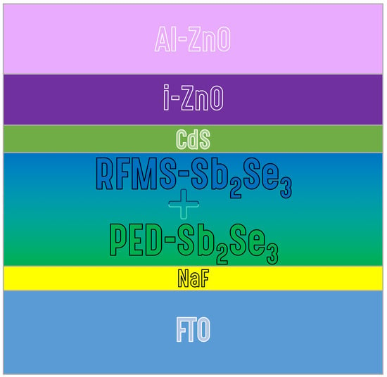
2. Materials and Methods

Sb2Se3 and NaF films were grown via PED using a high vacuum chamber, equipped with a PEBS-20 commercial source (supplied by Neocera Inc., Beltsville, MD, USA). The base pressure was around 2.0 × 10⁻⁴ Pa. The pulsed electron beam was ignited at a discharge voltage of 16 kV, with a pulse repetition rate of 9 Hz. During the deposition process, Ar gas (5N purity) pressure was of about 3.0 × 10⁻¹ Pa to ensure the stable and controlled emission of electrons towards the target. The used targets were 10 mm thick cylindrical pieces sliced from polycrystalline Sb2Se3 ingots and 5 at.% Cu:Sb2Se3, synthesized thanks to a customized Czochralski reactor from elemental species (5N purity). The target–substrate distance was maintained at 8 cm. Substrates were first mounted in a load-lock chamber, then transferred inside the main chamber and heated under a graphite susceptor using halogen lamps. The substrate temperature, set to 280 °C for optimal performance, was monitored using a type-K thermocouple and a 2.4 μm IR pyrometer (model Endurance E3M, supplied by Fluke Process Instruments, Berlin, Germany) placed behind a ZnSe-bandpass viewport at an angle of 45° to the sample surface.
RFMS-grown Sb2Se3 films were grown using a 3″ RF magnetron sputtering cathode (Kenosistec Srl, Milan, Italy) powered at 30 W, using a 4N-purity binary Sb2Se3 target (supplied by Testbourne Ltd., Basingstoke, UK) as the starting material. The base pressure was maintained below 1 × 10⁻⁶ mbar. The target–substrate distance was 8 cm. During deposition, the working pressure was kept at 5.0 × 10⁻¹ Pa by filling the chamber with 5N-purity Ar gas. The substrate temperature was optimized to 300 °C and monitored using a type-K thermocouple. Substrates consisted of 2.5 × 2.5 cm2 sized commercial glass sheets coated with fluorine tin oxide (FTO). The substrates were cleaned before PED and RFMS depositions by sequentially rinsing them in acetone, ethanol, and isopropyl alcohol. The top undoped ZnO (UZO) and Al-doped ZnO (AZO) layers were deposited via RF magnetron sputtering (Angstrom Sciences) at room temperature (RT) and 120 W in Ar atmosphere (5.0 × 10⁻¹ Pa). Structural characterizations of the films, including their crystalline structure and preferred grain orientations, were determined via X-ray diffraction (XRD) using a Siemens D500 (Siemens, Berlin, Germany) diffractometer in Bragg–Brentano geometry. The morphological and compositional characterizations of the samples were obtained using the Zeiss Auriga Compact field-emission scanning electron microscope (FESEM) equipped with an energy-dispersive X-ray spectroscopy (EDX) detector (Oxford). For SEM imaging, the electron beam acceleration was set to 5 kV or 10 kV, while for EDX analysis, it was set to 20 kV. Photovoltaic devices were fabricated according to the following structure (from top to bottom): AZO/UZO/CdS/Sb2Se3/NaF/FTO/glass. Current density–voltage (J-V) characteristics were measured using the Keithley 2614B source meter and the ABET SUN 2000 AAB solar simulator under standard test conditions (AM 1.5G spectrum, 1000 W/m2 irradiance, and a cell temperature of 25 °C).

3. Results

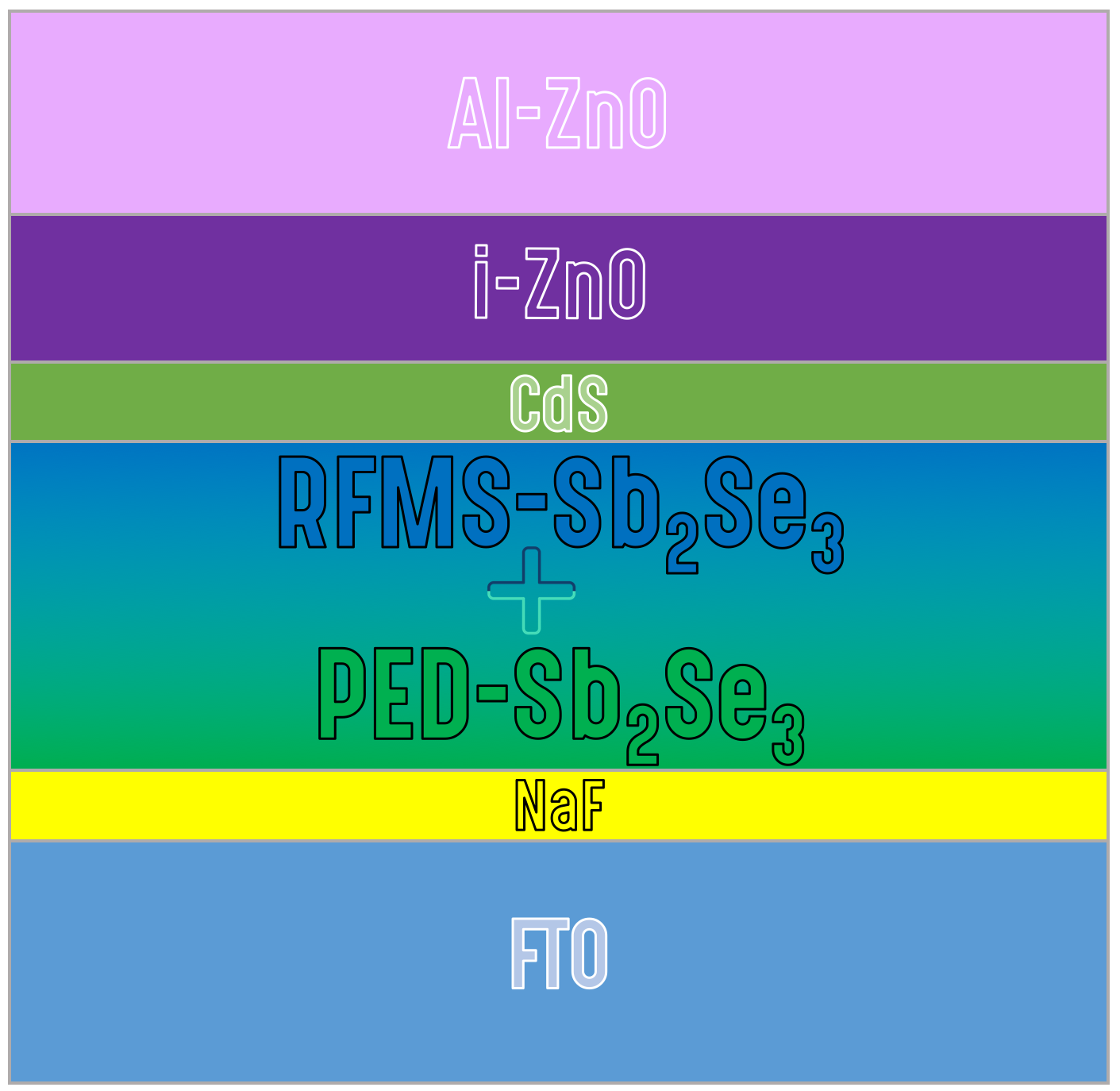
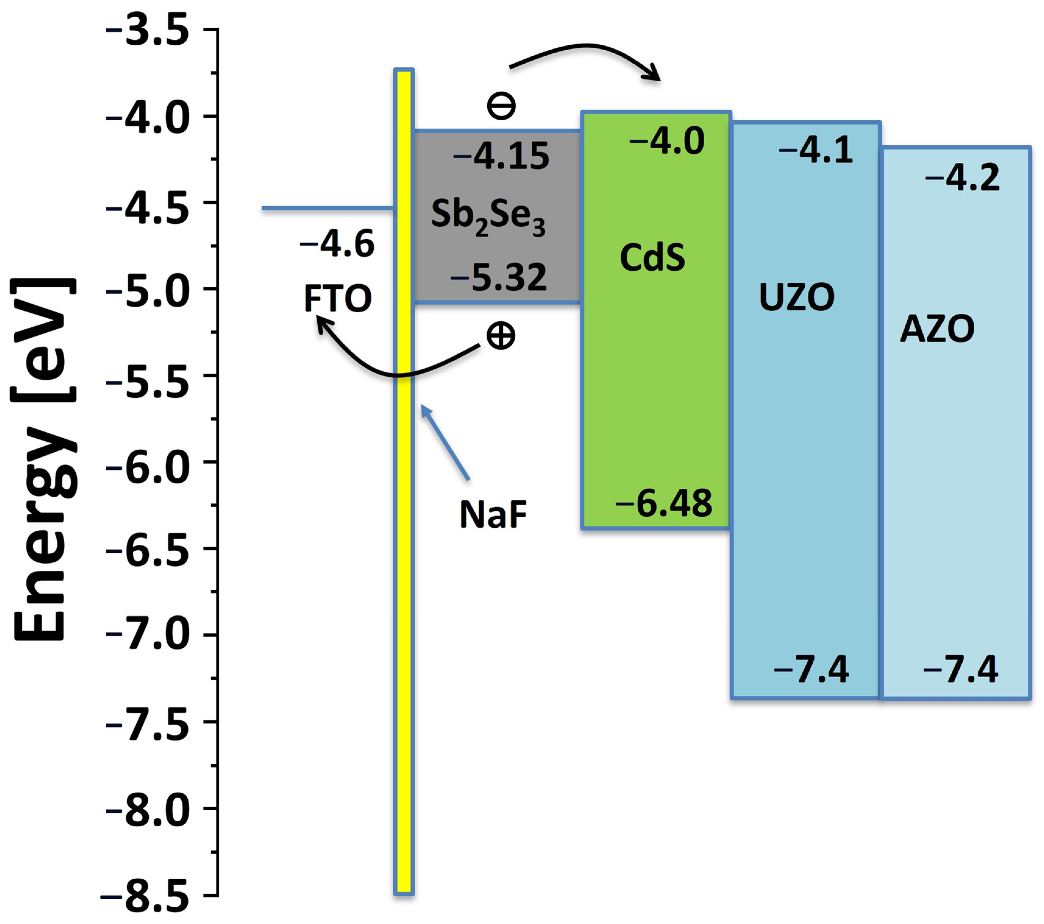
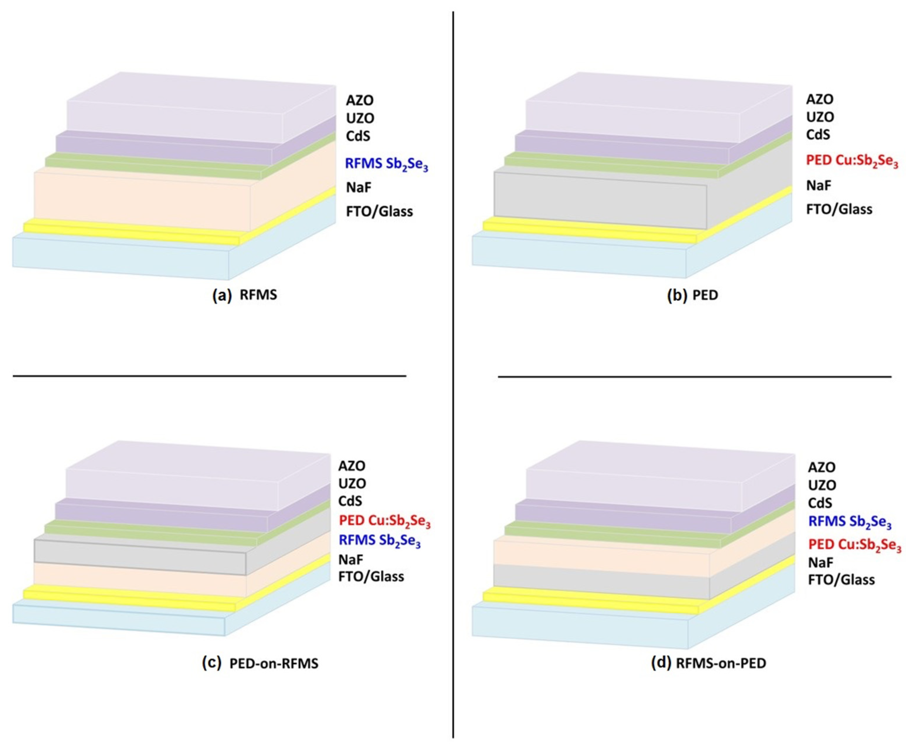
3.1. NaF Layer Effect on Sputtered and PED Sb2Se3 Based Solar Cells

In order to enhance photocarrier extraction at the FTO/Sb2Se3 interface, a 10 nm NaF thin layer was deposited via PED on the FTO/glass surface prior to Sb2Se3 deposition to examine its influence on photocarrier extraction. A schematic representation of the band diagram for the Sb2Se3-based solar cell with the NaF interlayer is shown in Figure 1. The enhanced p-doping effect of Na is attributed to (i) the substitution of Na for Sb at the interface (as Na presents a +1 oxidation state, while Sb +3); and (ii) the passivation of grain boundaries (GBs) and the associated defect states, as demonstrated in CIGS-based solar cells [29,30]. According to several models, Na effectively removes donor defects at grain boundaries, thereby reducing recombination traps and enhancing the carrier concentration in their vicinity. The NaF layer also introduces a controlled level of local doping at the interface, facilitating carrier tunneling through localized defect states. This strategy has been previously employed in bifacial CIGS-based solar cells, where a NaF layer was inserted at the CIGS/AZO interface to enhance carrier extraction at the transparent back contact [31].
We fabricated RFMS-grown and PED-grown Sb2Se3-based solar cells respectively with AZO/UZO/CdS/undoped-Sb2Se3/FTO/glass and AZO/UZO/CdS/Cu:Sb2Se3/FTO/glass structures. RFMS-grown Sb2Se3 layers exhibited a 2:3 Sb:Se stoichiometry and good homogeneity, as confirmed by EDX microanalysis reported in [17] (Figure S1, see Supplementary Material). In PED-grown Cu:Sb2Se3 layers, the 2:3 Sb:Se stoichiometry and the nominal 5% Cu atomic concentration were confirmed by EDX-SEM analysis both in the target and in the film. J-V curves in Figure 2a illustrate the photovoltaic performance of the sputtered Sb2Se3 solar cell. The incorporation of a NaF layer in the AZO/UZO/CdS/Sb2Se3/NaF/FTO/glass structure resulted in a significant enhancement of short-circuit current density (JSC) and open-circuit voltage (VOC), leading to an efficiency improvement from 1.28% to 3.2%.
Solar cells based on PED-grown 5%Cu:Sb2Se3 as the p-type layer with the same AZO/UZO/CdS/Cu:Sb2Se3/FTO/glass structure present higher VOC than undoped PED-grown Sb2Se3 (0.35 V–0.51 V as reported also by [25] vs. 0.26 V as reported by [32]). However, these PED-grown cells also exhibit very low short-circuit currents (JSC) (around 0.3 mA/cm2). The introduction of a NaF interfacial layer leads to a significant tenfold increase in JSC for this type of PED-grown solar cell (Figure 2b). The JSC enhancement induced by Na is substantial; however, JSC values for PED-grown Sb2Se3 are generally much lower than those for sputtered Sb2Se3, resulting in a power conversion efficiency (PCE) of only 0.36%.
The trap-assisted tunneling effect induced by Na at the FTO/ Sb2Se3 interface is supported by studying the effects of annealing treatments. As shown in Figure S2, the VOC of the PED-grown Cu:Sb2Se3 cell increases after different annealing cycles at 175 °C in air, and conversely, JSC is reduced. During the annealing process, Na atoms from the NaF layer are expected to diffuse from the interface to the Sb2Se3 bulk, passivating the GBs and other compensating defects [29,30]. However, as the defect density at the interface decreases, the tunneling through localized states is also reduced, resulting in a lower photocarrier extraction and, consequently, in a lower JSC. A recent study [33] also reported similar effects on improved electrical performance, particularly VOC, due to the inclusion of a NaF layer between the back contact and Sb2Se3. The study suggests that the diffusion of Na ions in the Sb2Se3 absorber layer could positively passivate defects at the bulk and heterojunction interface, thereby reducing defect-assisted recombination within the bulk.
The Cu:Sb2Se3 layer deposited via PED shows a free carrier density larger by two orders of magnitude with respect to undoped Sb2Se3 films, but it shows a very limited JSC. This observation could be attributed to a potential barrier that Cu ions create for photocarrier extraction at either the FTO/Cu:Sb2Se3 or Cu:Sb2Se3/CdS interfaces. In the former case, Cu ions may raise the minimum conduction band energy (since the minimum conduction band of CuSbSe2 is at −4.07 eV [34]), thereby enhancing the band offset with FTO and impeding the extraction of photogenerated charge carriers. Alternatively, the non-perpendicular orientation of [Sb4Se6]n ribbons within the PED-grown 5%Cu:Sb2Se3 layer could hinder photocarrier conduction. Despite the restricted JSC, PED-grown Sb2Se3 solar cells consistently exhibit higher VOC and fill factor (FF) values, indicating reduced non-radiative recombination and overall superior crystal quality.

3.2. Fabrication of Bi-Layered PED/Sputtering Sb2Se3 Solar Cells

Since carrier recombination is significantly reduced in PED-grown Sb2Se3, while RFMS enhances the alignment of ribbons and minimizes the photocurrent barrier, we deposited Sb2Se3 bilayers sequentially using both PED and RFMS techniques. This hybrid approach was effectively investigated in a recent literature study [35], in which two other techniques were utilized to fabricate graded Sb2(Se,S)3 multilayers, taking advantage of the distinct properties of each technique. Our hypothesis suggests that optimizing the electrical parameters (VOC and FF in the PED layer, JSC in the RFMS layer) in the PED-RFMS bilayers can enhance the overall efficacy of the solar cell. The thicknesses and deposition order of the two layers were systematically varied to investigate their impact in the structure and their behavior with the FTO and CdS interfaces. The various bilayer architectures are presented in Figure 3. The sample types and corresponding thicknesses are detailed in Table 1 for PED-on-RFMS bilayers and in Table 2 for RFMS-on-PED bilayers.
Table 1 contains a list of all the samples (A-series) in which the first layer is deposited with RFMS, followed by the PED film (PED-on-RFMS) (Figure 3c). Sample A1 corresponds to a single thick sputtered Sb2Se3 layer (Figure 3a). Table 2 lists all samples (B-series) in which the first layer is deposited with PED, followed by a sputtered layer (RFMS-on-PED) (Figure 3d). Sample B1 corresponds to a single thick layer deposited via PED (Figure 3b). The A samples have the following structure: AZO/UZO/CdS/Cu:Sb2Se3(PED)/Sb2Se3 (RFMS)/NaF/FTO/glass, while the B-series are fabricated with the inverse sequence of Cu:Sb2Se3 grown first via PED on NaF/FTO, followed by a sputtered Sb2Se3 layer (AZO/UZO/CdS/Sb2Se3(RFMS)/Cu:Sb2Se3 (PED)/NaF/FTO/glass).

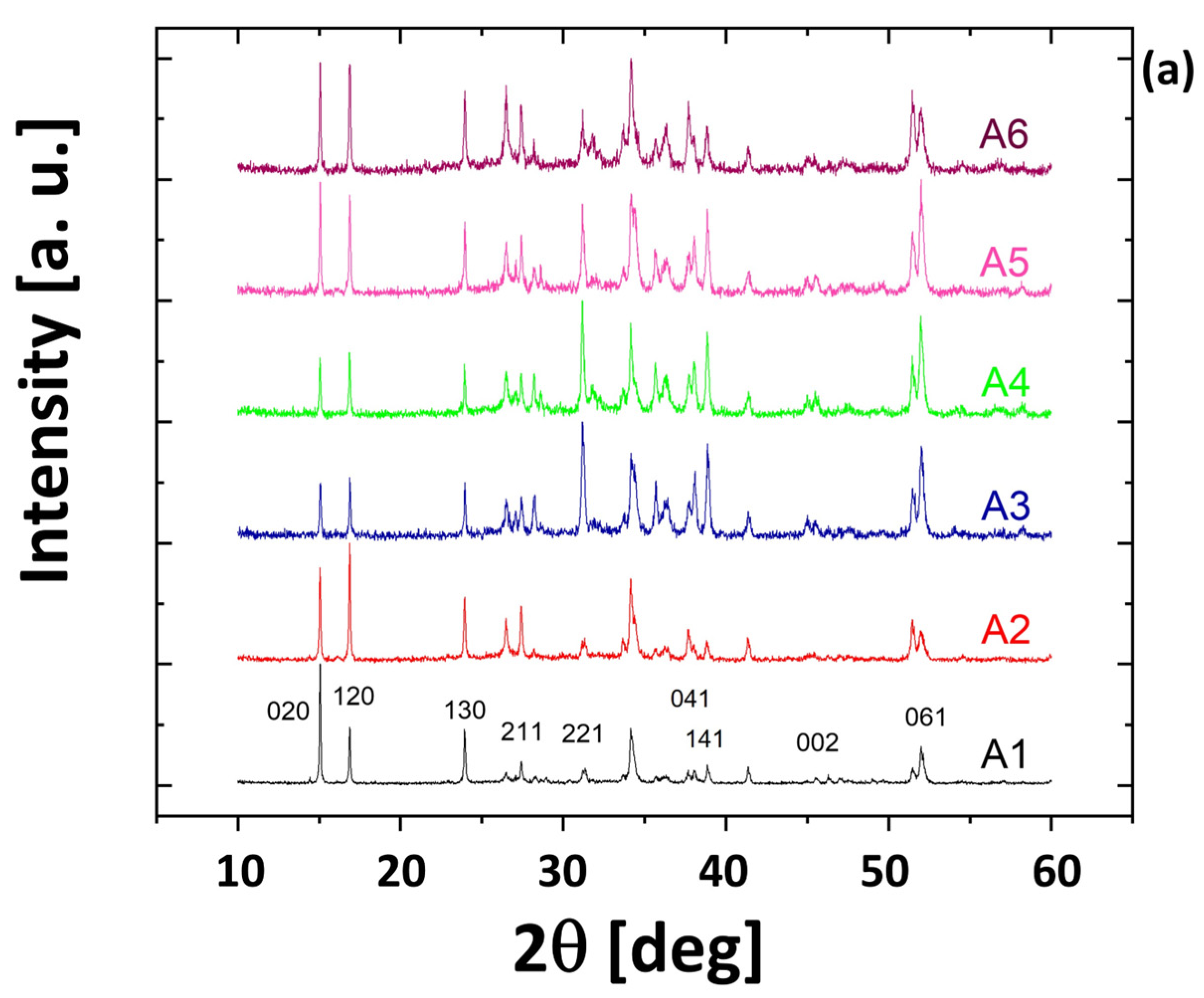
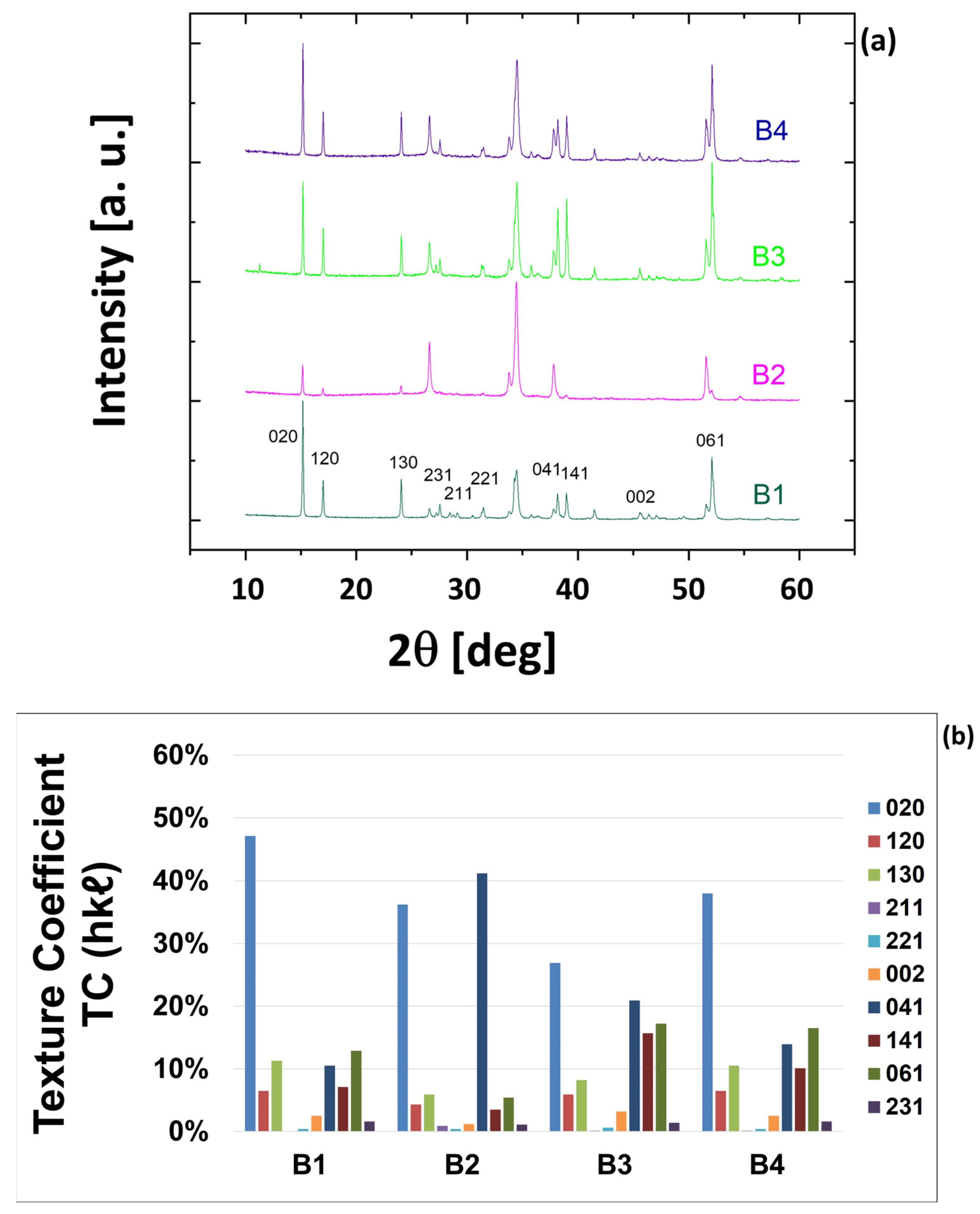
3.3. Structural Analysis

XRD patterns of Sb2Se3-based solar cells were collected to determine the preferential orientation of these films (Figure 4), using the Sb2Se3 orthorhombic phase as the reference (Ref. JCPDS 15–0681). The relative texture coefficient, TC (hkℓ), was calculated to compare ribbon orientation in all the layers and bilayers. TC (hkℓ) is the ratio between the measured (hkℓ) peak intensity and the intensity of the same peak for the reference randomly-oriented powder, weighted as a percentage on the summation of the same value for all chosen peaks [36,37], as expressed by the following formula:
T C h k l = I ( h k l ) I 0 ( h k l ) n I ( h k l ) I 0 ( h k l ) × 100 %
where I0 (hkℓ) is the relative intensity of the reflection with (hkℓ) Miller indices reported in the JCPDS card, and I (hkℓ) is the net intensity measured by the experimental XRD patterns after the background subtraction. A good crystalline quality can be observed for all the films, as testified by the low full-width half-maximum values of the reflections. In most of the cases, the (hk0) are the preferred crystal orientations, with the ribbons lying on the surface, already seen for this kind of growth [32]. However, (hkℓ) orientations with ℓ ≠ 0, especially the (041), (061) and (141) ones, are more intense or comparable to the (hk0) peaks in some bilayers such as in the A3, A4, A5 and B3 samples. In general, the (041), (061) and (141) reflections become predominant when the sputtered layer is thicker.
Figure 4b presents the TC values for the principal crystal orientations of the A-series samples. Similarly, Figure 5b depicts the TC values for the B-series samples. Based on its definition in Equation (1), when the texture coefficient (TC) exceeds 10%, a preferred orientation of grains in Sb2Se3 films along one or more of the 10 detected crystallographic directions is observed. Table 3 presents the values of ΣTC(ℓ ≠ 0), representing the sum of all TC values for hkl reflections with ℓ ≠ 0 for each sample analyzed in this study.

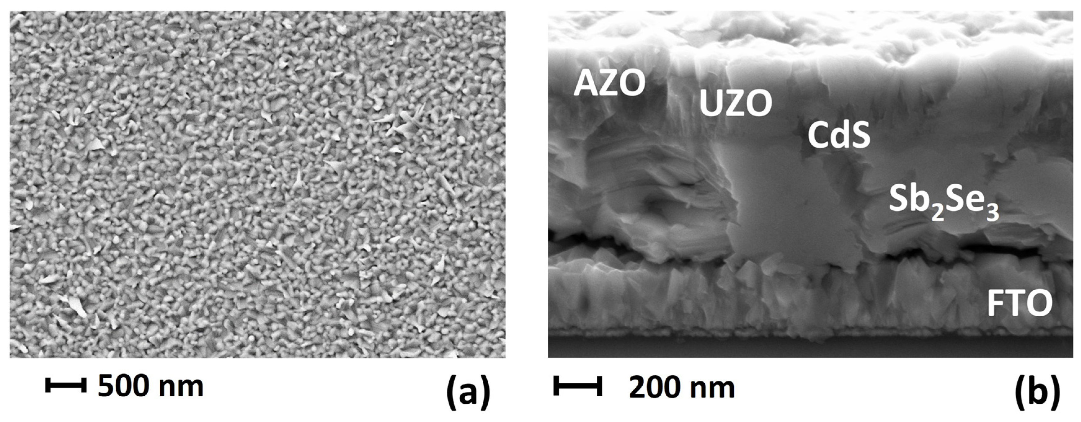
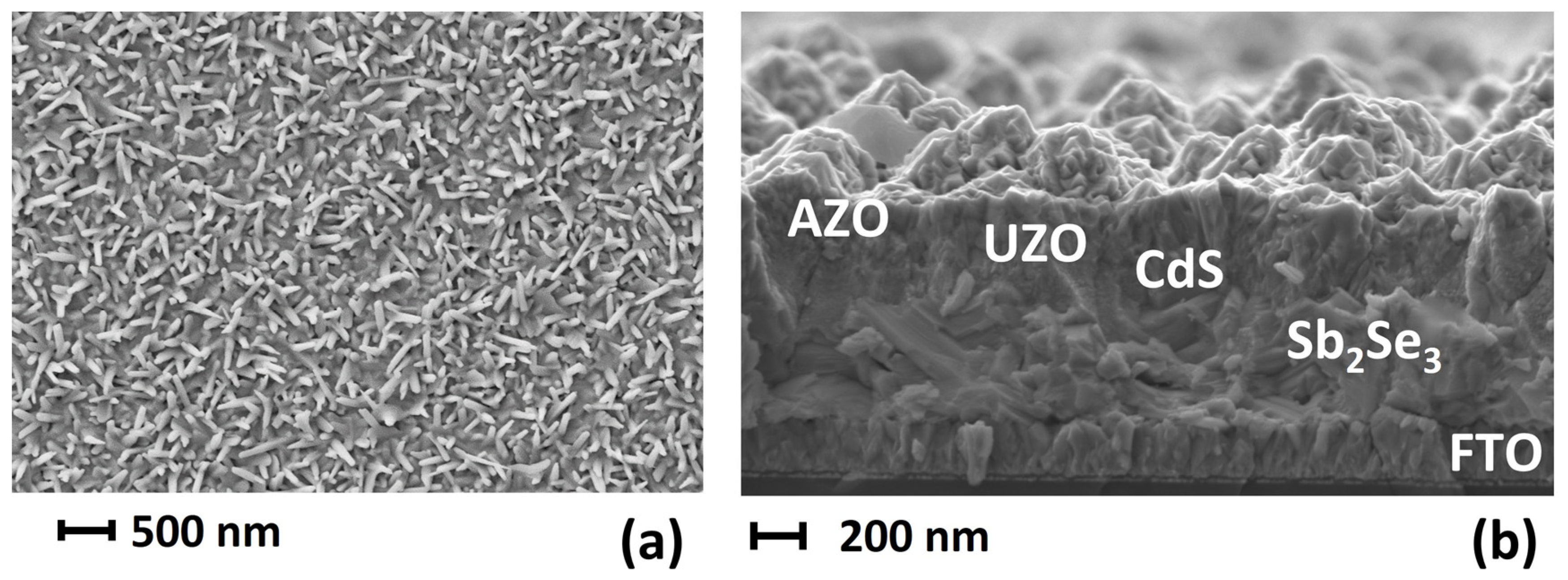
3.4. Morphological Analysis

As shown in SEM cross-sectional micrographs (Figure 6b and Figure 7b), the layers grown via PED and RFMS in the bilayer architecture exhibit no morphological differences, indicating a well-defined crystal structure throughout the active region of the cells. However, planar images reveal a distinct morphological contrast between the RFMS-grown layer in the B4 cell (Figure 6a) and the PED-grown layer (Figure 7a). The former layer exhibits a flatter surface morphology, while the PED-grown layer exhibits a needle-like morphology.

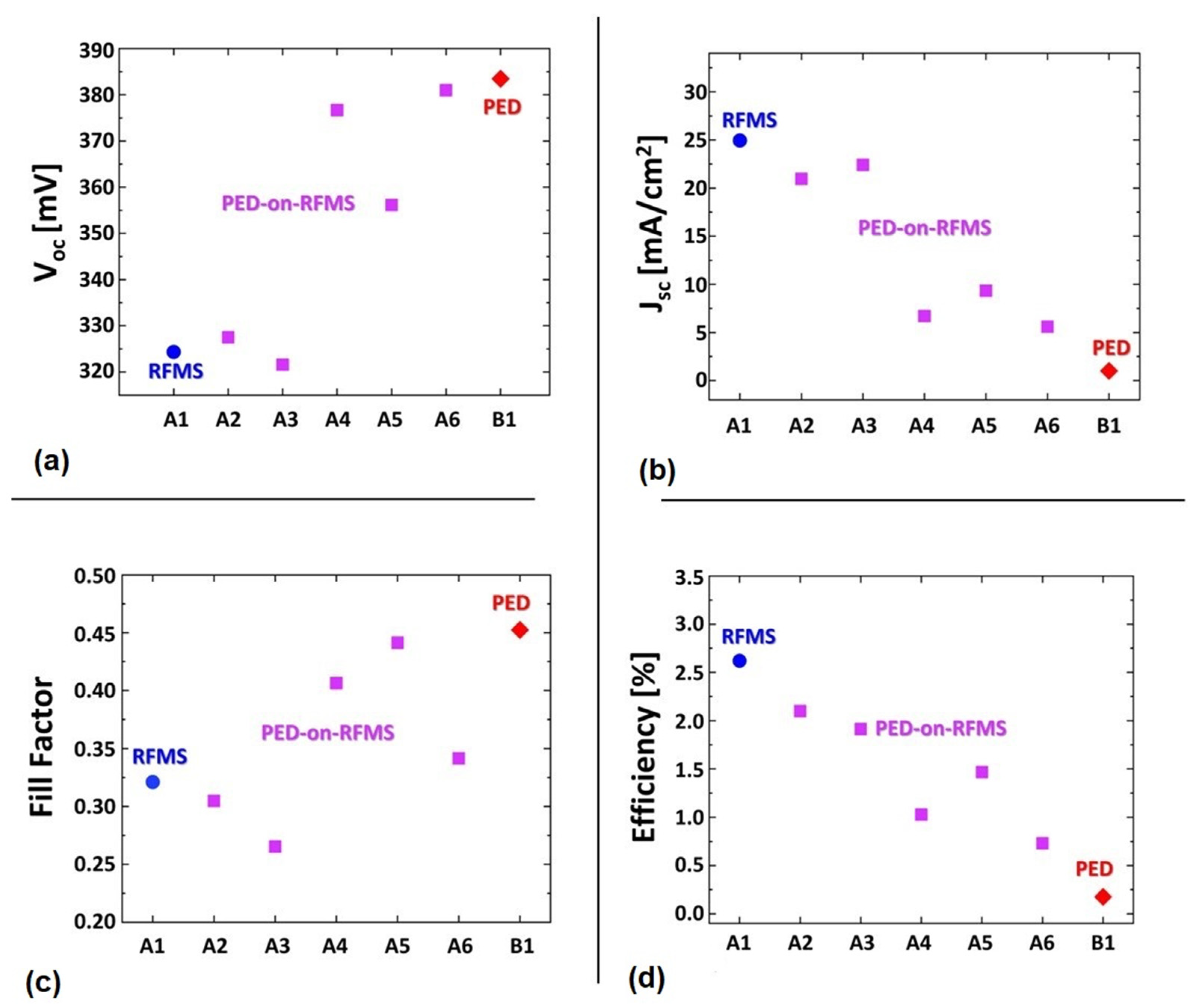
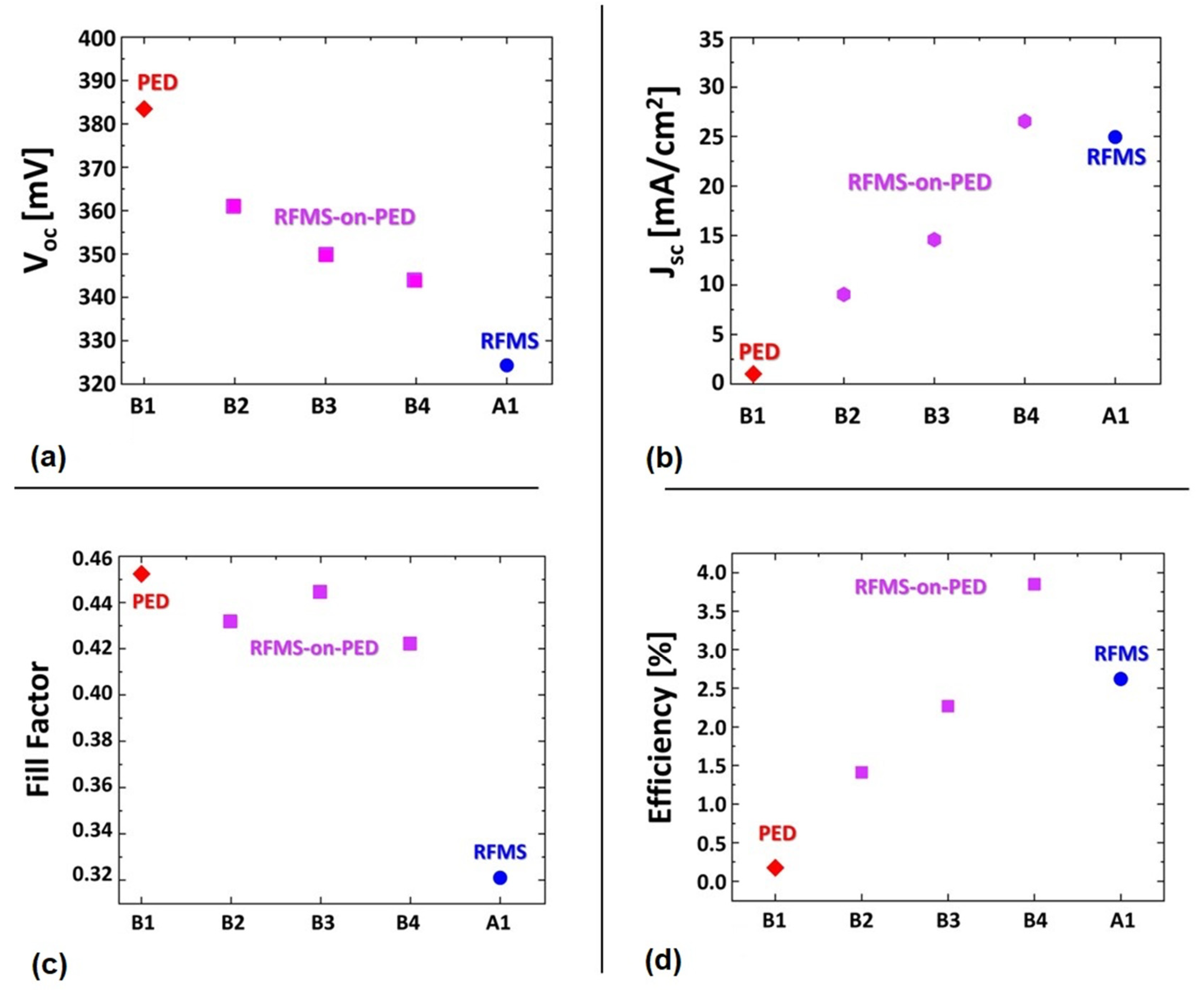
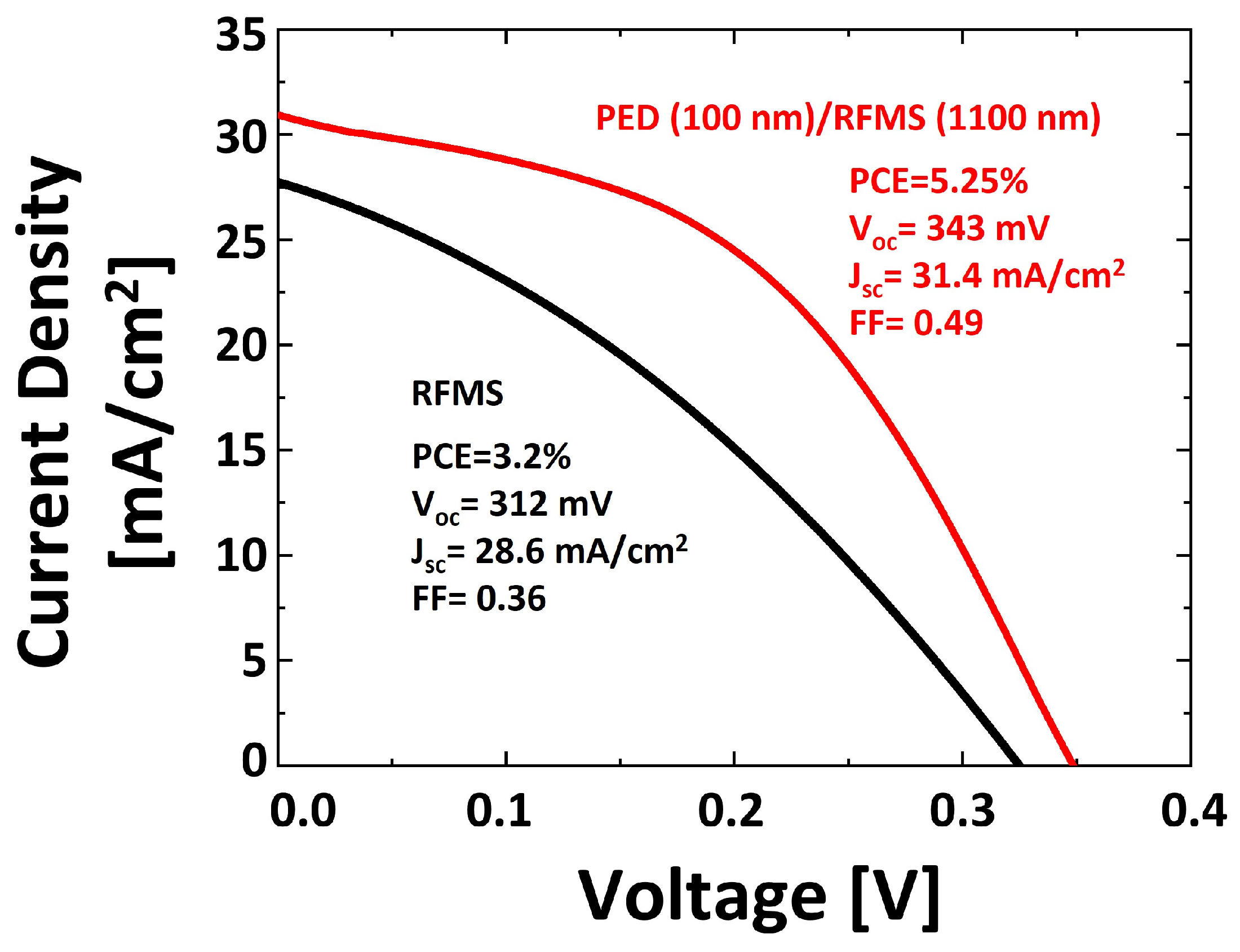
3.5. Solar Cell Performance and Characterization

The electrical performances of the fabricated devices are plotted in Figure 8 and Figure 9. The A samples, corresponding to the bilayer PED-on-RFMS architecture, are compared to the corresponding cells fabricated with a single layer of RFMS-grown (A1) and PED-grown (B1) Sb2Se3. As mentioned earlier, the B1 device is used as the reference for the highest values of the VOC and FF of a single layer, while A1 is the reference for the maximum JSC. As one can see in Figure 8, in the bilayer PED-on-RFMS architecture, VOC and FF increase with increasing PED layer thickness. In contrast, JSC decreases significantly for thicker PED layers, leading to lower overall solar cell efficiencies. In this set of samples, the electrical quantities exhibit a monotonic trend, transitioning from the characteristics of a single RFMS cell to those of a single PED cell and vice versa. When the RFMS layer is thicker, the bilayer cell exhibits properties similar to the A1 cell, characterized by high JSC but lower VOC and FF, while the performance of the bilayer cell approaches that of the B1 cell with increasing thickness of the upper PED layer. Despite the increase in VOC with thicker PED layers, no bilayer configuration surpasses the efficiency of the A1 cell with a single RFMS layer.
The electrical performances of the B-series solar cells (RFMS-on-PED) are depicted in Figure 9, compared to the reference cells made using single sputtered-grown (A1) and single PED-grown (B1) absorber layers. Consistent with the earlier results, the VOC and FF tend to increase with thicker PED-grown layers, while JSC decreases only for a PED-grown Cu:Sb2Se3 layer thicker than 100 nm. The B4 solar cell, consisting of a 100 nm PED-grown Cu:Sb2Se3 layer and a 1.1 μm sputtered-grown Sb2Se3 layer, exhibits the highest efficiency among the investigated devices.
Table 4 summarizes the average and record values for all the obtained devices. Furthermore, 20 solar cells with an area of 6 mm2 each were made and measured for each sample. It can be observed that samples with thicker Cu:Sb2Se3 PED-grown layers also generally show a narrower data spread, especially for JSC and PCE. In addition, they display higher Rsh, primarily caused by lower saturation currents, J0, which result in ideality factors, n, close to 1 and a higher FF. J0 values two–three orders of magnitude lower, especially for B-series cells in comparison with A1 and A2, indicate reduced bulk carrier recombination in PED-grown Cu:Sb2Se3 p-type layers. Since for Cu:Sb2Se3 PED-grown layers > 100 nm (B1, B2, B3, A4, A5, A6) JSC suffers from a dramatic decrease, one can argue that the presence of the PED Cu:Sb2Se3 bottom layer impedes photocarrier extraction. However, when this layer is < 100 nm, it does not appear to significantly block the photogenerated holes from Sb2Se3 to FTO, but it does reduce leakage currents (leading to higher FF and Rsh values). In contrast, for Cu:Sb2Se3 PED-grown layers exceeding 100 nm, a negative blocking effect becomes dominant. The non-ideal ribbon orientation (TC with (hkℓ) orientations ℓ ≠ 0 is only 35% for the B1 cell) could only partially explain the blocking behavior of this layer, since A1 shows only a slightly larger TC with respect to B1, but no photocurrent barrier seems to exist. Other factors, such as band misalignment at the FTO/Cu:Sb2Se3 interface, likely contribute to this blocking effect, creating an energy barrier that impedes the flow of holes from Sb2Se3 to FTO. Additionally, a comparison of the A- and B-series cells with similar thicknesses (i.e., A6, with a record PCE = 0.73% with B2, with PCE = 1.41%, or A2, with PCE = 2.04%, with B4, with PCE = 3.85%, or also A3 with B3), reveals that the B-series cells, with a RMFS layer on the absorber surface before the CdS, generally exhibit a superior performance compared to the A-series cells. A superior interface quality between the second RFMS-grown Sb2Se3 layer and CdS is likely responsible for these results. As evident from the SEM top-view images in Figure 6a and Figure 7a, the rougher PED-grown surface likely contributes to the junction deterioration, since the UZO/AZO layers appear to penetrate more deeply into the PED-grown layer and degrade the CdS/Sb2Se3 interface, leading to a significantly leakier junction. Table 4 reveals a wide distribution of cell parameters. Therefore, more precise measurements were conducted on the samples using Ag paste and wire bonding techniques. The samples from A1 to B3 exhibit no significant improvement. The B4 cell demonstrates an absolute increase in efficiency of approximately 1.5%, representing a significant relative 50% improvement. Figure 10 compares the J-V curves of the best cells (A1 and B4) after enhancing the top and bottom contacts using Ag paste and wire bonding.
The best solar cell consisting of a AZO/UZO/CdS/Sb2Se3(RFMS)/Cu:Sb2Se3 (PED)/NaF/FTO/glass structure, where the Cu:Sb2Se3 PED grown layer is 100 nm and the sputtering layer is 1100 nm, exhibited PCE = 5.25%, VOC = 343 mV, JSC = 31.4 mA/cm2 and FF = 0.49 (red line). All the key electrical parameters of this cell are upgraded in comparison with those of the sputtered A1 solar cell (black line). The improvement is attributed to enhanced FF and VOC, thanks to the thin Cu:Sb2Se3 layer grown via PED. The remarkable PCE = 5.25% achieved by the bilayer cell beats previous records for devices employing single and undoped Sb2Se3 absorbers. This impressive feat surpasses the previous benchmark of 2.1% for a PED-grown Sb2Se3 cell reported in [32], as well as the 1.28% and 2.36% efficiencies obtained for RFMS-Sb2Se3 cells on FTO and CdS/FTO substrates, respectively [17]. The highest reported efficiency for an RFMS-grown Sb2Se3 cell is 6.06%, but this required an additional post-selenization step [38].

4. Conclusions

The results presented in this work show simple strategies of interfacial engineering for Sb2Se3 solar cells, which clearly improve their performance, and suggest viable architectures for Sb2Se3-based devices. The deposition of a NaF interface layer between the FTO back contact and Sb2Se3 p-region can improve JSC: Na, migrating from the NaF layer to Sb2Se3 can both passivate grain boundaries and favor carrier extraction through defect-assisted tunneling. The properties of the bi-layered absorber based on sputtered undoped Sb2Se3 and PED-grown Cu:Sb2Se3 sequentially grown in different thicknesses have also been analyzed. In particular, the RFMS-on-PED structure leads to a valuable maximum efficiency value = 5.25% when a very thin (maximum 100 nm) PED-grown layer is deposited onto NaF. The presence of this thin Cu-doped Sb2Se3 layer favors the enhancement of VOC and FF, in comparison to a solar cell with a completely sputtered Sb2Se3 p-region. While thicker PED-grown layers degrade the JSC, introducing a thin current blocking layer, a hole–electron charges separation limiting the photocarrier recombination and current leakage is obtained.

Supplementary Materials

The following supporting information can be downloaded at: https://www.mdpi.com/article/10.3390/solar4010004/s1, Figure S1: EDX mapping of composition for the stoichiometric (40/60 ratio) Sb2Se3 films acquired via scanning electron microscope (FE-SEMFIB, Zeiss Auriga Compact) equipped with an energy dispersive X-ray spectrometer (EDX, Oxford); Figure S2: From top: VOC, JSC and efficiency variation after annealing treatments compared with as-grown PED-grown 5%Cu:Sb2Se3 solar cells with AZO/UZO/CdS/Cu:Sb2Se3/FTO/glass structure.

Author Contributions

Conceptualization, R.J. and S.R.; methodology, R.J.; validation, F.P. and E.G.; formal analysis, K.K.S.; investigation, G.S., M.C., F.M., G.T., E.D.C. and M.B.; resources, S.R.; data curation, G.S.; writing—original draft preparation, R.J.; writing—review and editing, S.R. and F.P.; visualization, G.S.; supervision, F.P.; project administration, S.R.; funding acquisition, S.R. All authors have read and agreed to the published version of the manuscript.

Funding

This research was funded by the Italian Ministry of the Environment and Energy Security: Research Fund for the Italian Electrical System (type-A call, published on G.U.R.I. n. 192 on 18 August 2022). The research was also funded by the Italian Ministry of University and Research: “Ecosystem for Sustainable Transition in Emilia-Romagna” (EcosistER), funded under the National Recovery and Resilience Plan (NRRP), Mission 4 Component 2 Investment 1.5—Call for tender No. 3277 of 30 December 2021 of the Italian Ministry of University and Research funded by the European Union—NextGenerationEU.

Institutional Review Board Statement

Not applicable.

Informed Consent Statement

Not applicable.

Data Availability Statement

Data are contained within the article and supplementary materials.

Acknowledgments

Part of this work was supported by the Bio-MoNTANS project funded by Cariparma. Kodjo Kekeli Sossoe acknowledges the World Bank for the project “Centre d’Excellence Régional pour la Maîtrise de l’Electricité” of the University of Lomé (Crédit IDA 6512-TG; Don IDA 536IDA) and ICTP with the TRIL Program for Italian research institutions. The authors would like to thank the financial support of Coordenação de Aperfeiçoamento de Pessoal de Nível Superior (CAPES) Project PROCAD Defesa DRI 15/2019. This study is a result of the research project “nuovi Concetti, mAteriali e tecnologie per l’iNtegrazione del fotoVoltAico negli edifici in uno scenario di generazione diffuSa” (CANVAS), funded by the Italian Ministry of the Environment and Energy Security, through the Research Fund for the Italian Electrical System (type-A call, published on G.U.R.I. n. 192 on 18 August 2022). The work is part of the project “Ecosystem for Sustainable Transition in Emilia-Romagna” (Ecosister), funded under the National Recovery and Resilience Plan (NRRP), Mission 4 Component 2 Investment 1.5—Call for tender No. 3277 of 30 December 2021 of the Italian Ministry of University and Research funded by the European Union—NextGenerationEU.

Conflicts of Interest

The authors declare no conflicts of interest.

References

  1. Green, M.A.; Dunlop, E.D.; Yoshita, M.; Kopidakis, N.; Bothe, K.; Siefer, G.; Hao, X. Solar cell efficiency tables (version 62). Prog. Photovolt. 2023, 31, 651–663. [Google Scholar] [CrossRef]
  2. Yoshikawa, K.; Kawasaki, H.; Yoshida, W.; Irie, T.; Konishi, K.; Nakano, K.; Uto, T.; Adachi, D.; Kanematsu, M.; Uzu, H.; et al. Silicon heterojunction solar cell with interdigitated back contacts for a photoconversion efficiency over 26%. Nat. Energy 2017, 2, 17032. [Google Scholar] [CrossRef]
  3. Hameed, T.A.; Cao, W.; Mansour, B.A.; Elzawaway, I.K.; Abdelrazek, E.-M.M.; Elsayed-Ali, H.E. Properties of Cu(In,Ga,Al)Se2 thin films fabricated by magnetron sputtering. J. Vac. Sci. Technol. A 2015, 33, 031201. [Google Scholar] [CrossRef]
  4. Chen, C.; Li, K.; Tang, J. Ten Years of Sb2Se3 Thin Film Solar Cells. Solar RRL 2022, 6, 2200094. [Google Scholar] [CrossRef]
  5. Wang, J.; Li, K.; Tang, J.; Chen, C. A Perspective of Antimony Chalcogenide Photovoltaics toward Commercialization. Solar RRL 2023, 7, 2300436. [Google Scholar] [CrossRef]
  6. Liu, X.; Chen, J.; Luo, M.; Leng, M.; Xia, Z.; Zhou, Y.; Qin, S.; Xue, D.-J.; Lv, L.; Huang, H.; et al. Thermal Evaporation and Characterization of Sb2Se3 Thin Film for Substrate Sb2Se3/CdS Solar Cells. ACS Appl. Mater. Interfaces 2014, 6, 10687–10695. [Google Scholar] [CrossRef] [PubMed]
  7. Chen, S.; Fu, Y.; Ishaq, M.; Li, C.; Ren, D.; Su, Z.; Qiao, X.; Fan, P.; Liang, G.; Tang, J. Carrier recombination suppression and transport enhancement enable high-performance self-powered broadband Sb2Se3 photodetectors. InfoMat 2023, 5, e12400. [Google Scholar] [CrossRef]
  8. Shockley, W.; Queisser, H.J. Detailed Balance Limit of Efficiency of p-n Junction Solar Cells. J. Appl. Phys. 1961, 32, 510–519. [Google Scholar] [CrossRef]
  9. Zhao, Y.; Wang, S.; Li, C.; Che, B.; Chen, X.; Chen, H.; Tang, R.; Wang, X.; Chen, G.; Wang, T.; et al. Regulating deposition kinetics via a novel additive-assisted chemical bath deposition technology enables fabrication of 10.57%-efficiency Sb2Se3 solar cells. Energy Environ. Sci. 2022, 15, 5118–5128. [Google Scholar] [CrossRef]
  10. Zhou, Y.; Wang, L.; Chen, S.; Qin, S.; Liu, X.; Chen, J.; Xue, D.-J.; Luo, M.; Cao, Y.; Cheng, Y.; et al. Thin-film Sb2Se3 photovoltaics with oriented one-dimensional ribbons and benign grain boundaries. Nat. Photon. 2015, 9, 409–415. [Google Scholar] [CrossRef]
  11. Ganose, A.M.; Savory, C.N.; Scanlon, D.O. Beyond methylammonium lead iodide: Prospects for the emergent field of ns2 containing solar absorbers. Chem. Commun. 2017, 53, 20–44. [Google Scholar] [CrossRef] [PubMed]
  12. Choi, Y.C.; Mandal, T.N.; Yang, W.S.; Lee, Y.H.; Im, S.H.; Noh, J.H.; Seok, S.I. Sb2Se3-Sensitized Inorganic-Organic Heterojunction Solar Cells Fabricated Using a Single-Source Precursor. Angew. Chem. 2014, 126, 1353–1357. [Google Scholar] [CrossRef]
  13. Guo, H.; Zhao, C.; Xing, Y.; Tian, H.; Yan, D.; Zhang, S.; Jia, X.; Qiu, J.; Yuan, N.; Ding, J. High-Efficiency Sb2Se3 Solar Cells Modified by Potassium Hydroxide. J. Phys. Chem. Lett. 2021, 12, 12352–12359. [Google Scholar] [CrossRef]
  14. Chen, C.; Li, K.; Chen, S.; Wang, L.; Lu, S.; Liu, Y.; Li, D.; Song, H.; Tang, J. Efficiency Improvement of Sb2Se3 Solar Cells via Grain Boundary Inversion. ACS Energy Lett. 2018, 3, 2335–2341. [Google Scholar] [CrossRef]
  15. Liang, G.-X.; Zhang, X.-H.; Ma, H.-L.; Hu, J.-G.; Fan, B.; Luo, Z.-K.; Zheng, Z.-H.; Luo, J.-T.; Fan, P. Facile preparation and enhanced photoelectrical performance of Sb2Se3 nano-rods by magnetron sputtering deposition. Sol. Energy Mater. Sol. Cells 2017, 160, 257–262. [Google Scholar] [CrossRef]
  16. Tang, R.; Chen, X.-Y.; Liang, G.-X.; Su, Z.-H.; Luo, J.; Fan, P. Magnetron sputtering deposition and selenization of Sb2Se3 thin film for substrate Sb2Se3/CdS solar cells. Surf. Coat. Technol. 2019, 360, 68–72. [Google Scholar] [CrossRef]
  17. Spaggiari, G.; Pattini, F.; Bersani, D.; Calestani, D.; De Iacovo, A.; Gilioli, E.; Mezzadri, F.; Sala, A.; Trevisi, G.; Rampino, S. Growth and structural characterization of Sb2Se3 solar cells with vertical Sb4Se6 ribbon alignment by RF magnetron sputtering. J. Phys. D Appl. Phys. 2021, 54, 385502. [Google Scholar] [CrossRef]
  18. Park, S.-N.; Kim, S.-Y.; Lee, S.-J.; Sung, S.-J.; Yang, K.-J.; Kang, J.-K.; Kim, D.-H. Controlled synthesis of (hk1) preferentially oriented Sb2Se3 rod arrays by co-evaporation for photovoltaic applications. J. Mater. Chem. A 2019, 7, 25900–25907. [Google Scholar] [CrossRef]
  19. Guo, L.; Zhang, B.; Qin, Y.; Li, D.; Li, L.; Qian, X.; Yan, F. Tunable Quasi-One-Dimensional Ribbon Enhanced Light Absorption in Sb2Se3 Thin-Film Solar Cells Grown by Close-Space Sublimation. Solar RRL 2018, 2, 1800128. [Google Scholar] [CrossRef]
  20. Tao, R.; Tan, T.; Zhang, H.; Meng, Q.; Zha, G. Sb2Se3 solar cells fabricated via close-space sublimation. J. Vac. Sci. Technol. B Nanotechnol. Microelectron. Mater. Process. Meas. Phenom. 2021, 39, 052203. [Google Scholar] [CrossRef]
  21. Li, Z.; Liang, X.; Li, G.; Liu, H.; Zhang, H.; Guo, J.; Chen, J.; Shen, K.; San, X.; Yu, W.; et al. 9.2%-efficient core-shell structured antimony selenide nanorod array solar cells. Nat. Commun. 2019, 10, 125. [Google Scholar] [CrossRef]
  22. Duan, Z.; Liang, X.; Feng, Y.; Ma, H.; Liang, B.; Wang, Y.; Luo, S.; Wang, S.; Schropp, R.E.I.; Mai, Y.; et al. Sb2Se3 Thin-Film Solar Cells Exceeding 10% Power Conversion Efficiency Enabled by Injection Vapor Deposition Technology. Adv. Mater. 2022, 34, 2202969. [Google Scholar] [CrossRef]
  23. Bosio, A.; Foti, G.; Pasini, S.; Spoltore, D. A Review on the Fundamental Properties of Sb2Se3-Based Thin Film Solar Cells. Energies 2023, 16, 6862. [Google Scholar] [CrossRef]
  24. Li, W.-H.; Li, M.; Hu, Y.-J.; Cheng, C.-H.; Kan, Z.-M.; Yu, D.; Leng, J.; Jin, S.; Cong, S. Enhanced performance of antimony selenide thin film solar cell using PbI2 as a dopant. Appl. Phys. Lett. 2021, 118, 093903. [Google Scholar] [CrossRef]
  25. Spaggiari, G.; Bersani, D.; Calestani, D.; Gilioli, E.; Gombia, E.; Mezzadri, F.; Casappa, M.; Pattini, F.; Trevisi, G.; Rampino, S. Exploring Cu-Doping for Performance Improvement in Sb2Se3 Photovoltaic Solar Cells. Int. J. Mol. Sci. 2022, 23, 15529. [Google Scholar] [CrossRef]
  26. Hobson, T.D.C.; Shiel, H.; Savory, C.N.; Swallow, J.E.N.; Jones, L.A.H.; Featherstone, T.J.; Smiles, M.J.; Thakur, P.K.; Lee, T.-L.; Das, B.; et al. P-type conductivity in Sn-doped Sb2Se3. J. Phys. Energy 2022, 4, 045006. [Google Scholar] [CrossRef]
  27. Li, Y.; Zhou, Y.; Luo, J.; Chen, W.; Yang, B.; Wen, X.; Lu, S.; Chen, C.; Zeng, K.; Song, H.; et al. The effect of sodium on antimony selenide thin film solar cells. RSC Adv. 2016, 6, 87288–87293. [Google Scholar] [CrossRef]
  28. Ren, D.; Chen, S.; Cathelinaud, M.; Liang, G.; Ma, H.; Zhang, X. Fundamental Physical Characterization of Sb2Se3-Based Quasi-Homojunction Thin Film Solar Cells. ACS Appl. Mater. Interfaces 2020, 12, 30572–30583. [Google Scholar] [CrossRef]
  29. Mungan, E.S.; Wang, X.; Alam, M.A. Modeling the Effects of Na Incorporation on CIGS Solar Cells. IEEE J. Photovolt. 2013, 3, 451–456. [Google Scholar] [CrossRef]
  30. Urbaniak, A.; Igalson, M.; Pianezzi, F.; Bücheler, S.; Chirilă, A.; Reinhard, P.; Tiwari, A.N. Effects of Na incorporation on electrical properties of Cu(In,Ga)Se2-based photovoltaic devices on polyimide substrates. Sol. Energy Mater. Sol. Cells 2014, 128, 52–56. [Google Scholar] [CrossRef]
  31. Cavallari, N.; Pattini, F.; Rampino, S.; Annoni, F.; Barozzi, M.; Bronzoni, M.; Gilioli, E.; Gombia, E.; Maragliano, C.; Mazzer, M.; et al. Low temperature deposition of bifacial CIGS solar cells on Al-doped Zinc Oxide back contacts. Appl. Surf. Sci. 2017, 412, 52–57. [Google Scholar] [CrossRef]
  32. Pattini, F.; Rampino, S.; Mezzadri, F.; Calestani, D.; Spaggiari, G.; Sidoli, M.; Delmonte, D.; Sala, A.; Gilioli, E.; Mazzer, M. Role of the substrates in the ribbon orientation of Sb2Se3 films grown by Low-Temperature Pulsed Electron Deposition. Sol. Energy Mater. Sol. Cells 2020, 218, 110724. [Google Scholar] [CrossRef]
  33. Chen, M.; Ishaq, M.; Ren, D.; Ma, H.; Su, Z.; Fan, P.; Le Coq, D.; Zhang, X.; Liang, G.; Chen, S. Interface optimization and defects suppression via NaF introduction enable efficient flexible Sb2Se3 thin-film solar cells. J. Energy Chem. 2024, 90, 165–175. [Google Scholar] [CrossRef]
  34. Wada, T.; Maeda, T. Optical properties and electronic structures of CuSbS2, CuSbSe2, and CuSb(S1−xSex)2 solid solution. Phys. Status Solidi C 2017, 14, 1600196. [Google Scholar] [CrossRef]
  35. Wang, Y.; Ji, S.; Moon, C.; Chu, J.; Jung, H.J.; Shin, B. Efficiency boosting in Sb2(S,Se)3 solar cells enabled by tailoring bandgap gradient via a hybrid growth method. J. Mater. Chem. A 2023, 11, 23071–23079. [Google Scholar] [CrossRef]
  36. Bérubé, L.P.; L’Espérance, G. A Quantitative Method of Determining the Degree of Texture of Zinc Electrodeposits. J. Electrochem. Soc. 1989, 136, 2314–2315. [Google Scholar] [CrossRef]
  37. Hameed, T.A.; Sharmoukh, W.; Anis, B.; Youssef, A.M. Enhanced photocatalytic activity and diode performance of ZnO-GO nanocomposites via doping with aluminum. Int. J. Energy Res. 2022, 46, 22601–22624. [Google Scholar] [CrossRef]
  38. Tang, R.; Zheng, Z.-H.; Su, Z.-H.; Li, X.-J.; Wei, Y.-D.; Fu, Y.-Q.; Luo, J.-T. Highly Efficient and Stable Planar Heterojunction Solar Cell Based on Sputtered and Post-Selenized Sb2Se3 Thin Film. Nano Energy 2019, 64, 103929. [Google Scholar] [CrossRef]
Figure 1. Band diagram of the AZO/UZO/CdS/Sb2Se3/NaF/FTO/glass solar cell.
Solar 04 00004 g001
Figure 2. Illuminated current density–voltage (J-V) characteristics of (a) an RFMS-grown Sb2Se3 solar cell with and without NaF interlayer; (b) a PED-grown Cu:Sb2Se3 solar cell with and without NaF interlayer.
Solar 04 00004 g002
Figure 3. Schematic solar cell geometry of (a) the completely sputtering-grown A1, (b) the completely PED-grown B1, (c) PED on sputtering bilayer architecture (A2 to A6) and (d) sputtering on PED bilayer architecture (B2 to B4).
Solar 04 00004 g003
Figure 4. (a) XRD patterns of the A-series solar cells based on PED-on-RFMS Sb2Se3 bilayer grown on FTO/soda-lime glass substrates; (b) histogram of the TC values of the fabricated samples for different (hkℓ) reflections.
Solar 04 00004 g004aSolar 04 00004 g004b
Figure 5. (a) XRD patterns of the B-series solar cells based on RFMS-on-PED Sb2Se3 bilayer grown on FTO/soda-lime glass substrates; (b) histogram of the TC values of the fabricated samples for different (hkℓ) reflections.
Solar 04 00004 g005
Figure 6. (a) SEM micrograph of the Cu:Sb2Se3 surface of an RFMS-on-PED bilayer Sb2Se3 solar cell and (b) the corresponding cross-sectional image.
Solar 04 00004 g006
Figure 7. (a) SEM micrograph of the Sb2Se3 surface of a PED-on-RFMS bilayer Sb2Se3 solar cell and (b) the corresponding cross-sectional image.
Solar 04 00004 g007
Figure 8. Photovoltaic performances—(a) Voc, (b) Jsc, (c) FF, and (d) Efficiency - of the different A-series solar cells (violet squares) compared to the completely PED-grown Cu:Sb2Se3 solar cell (red diamond), B1, and the completely sputtered Sb2Se3 solar cell (blue circle), A1.
Solar 04 00004 g008
Figure 9. Photovoltaic performances—(a) Voc, (b) Jsc, (c) FF, and (d) Efficiency - of the different B-series solar cells (purple squares). The completely PED-grown Sb2Se3 solar cell (red diamond), B1, and the completely sputtered Sb2Se3 solar cell (blue circle), A1, are used for benchmarking.
Solar 04 00004 g009
Figure 10. The current density–voltage (J-V curve) of the best Sb2Se3 cells obtained entirely via sputtering (Sample A1, black curve) and the bilayered RFMS-on-PED B4 structure (red curve).
Solar 04 00004 g010
Table 1. List of bilayered samples with PED-on-RFMS Sb2Se3 architecture and their corresponding layer thickness.
SampleSputtering Layer
(nm)
PED Layer
(nm)
A112000
A21100100
A3950250
A4800400
A5400800
A62001000
Table 2. List of bilayered samples with RFMS-on-PED Sb2Se3 architecture and their corresponding layer thickness.
SamplePED Layer
(nm)
Sputtering Layer
(nm)
B112000
B21000200
B32001000
B41001100
Table 3. ΣTC (ℓ ≠ 0) values of the different studied samples.
SampleΣTC (ℓ ≠ 0)
(%)
A143.36
A228.63
A366.43
A465.33
A554.65
A621.82
B135.04
B253.65
B359.04
B445.05
Table 4. Average and record (between parentheses) device parameters of the different Sb2Se3-based solar cells.
SampleVOC
(mV)
JSC
(mA/cm2)
FF
(%)
PCE
(%)
Rs
(Ωcm2)
Rsh
(Ωcm2)
J0
(mA/cm2)
n
A1305 ± 32 (324)22.5 ± 6.6 (31.2)29.3 ± 2.2 (32.0)2.03 ± 0.66 (3.24)6.86342.76.7 × 10−32.7
A2296 ± 62 (327)9.15 ± 7.66 (20.95)37.2 ± 8 (30.4)0.9 ± 0.6 (2.04)4.17149.29.5 × 10−43.5
A3343 ± 43 (321)9.35 ± 7.5 (22.4)33.9 ± 4.5 (26.5)0.93 ± 0.52 (1.91)18.344566.66.7 × 10−52.4
A4373 ± 9 (377)5.46 ± 0.95 (6.7)37.1 ± 1.9 (40.6)0.76 ± 0.16 (1.02)9.055754.47.4 × 10−51.3
A5342 ± 22 (356)8.08 ± 1.7 (9.32)41.3 ± 5.4 (44.0)1.15 ± 0.28 (1.47)3.6405.91.7 × 10−32.5
A6395 ± 13 (381)3.67 ± 1.18 (5.58)35.3 ± 1.1 (34.0)0.51 ± 0.14 (0.73)4.4526,833.27.6 × 10−61.3
B1385 ± 19 (355)0.74 ± 0.2 (1.25)42.6 ± 3.7 (40.6)0.12 ± 0.02 (0.18)3.7521,298.04.6 × 10−61.4
B2359 ± 3 (361)9.07 ± 0.47 (9.05)41.1 ± 1.9 (43.2)1.35 ± 0.06
(1.41)
2.353314.17.2 × 10−51.3
B3358 ± 7 (349)9.89 ± 2.6 (14.58)45.0 ± 2.5 (44.5)1.58 ± 0.38 (2.27)4.591633.48.5 × 10−51.4
B4347 ± 7 (344)14.65 ± 3.3 (26.6)48.8 ± 3.5 (42.2)2.45 ± 0.39 (3.85)1.81460.25.4 × 10−51.3
Disclaimer/Publisher’s Note: The statements, opinions and data contained in all publications are solely those of the individual author(s) and contributor(s) and not of MDPI and/or the editor(s). MDPI and/or the editor(s) disclaim responsibility for any injury to people or property resulting from any ideas, methods, instructions or products referred to in the content.

