Article

Solar Cells with Laser Doped Boron Layers from Atmospheric Pressure Chemical Vapor Deposition

1
Institute of Photovoltaics and Research Center SCoPE, University of Stuttgart, Pfaffenwaldring 47, 70569 Stuttgart, Germany
2
SCHMID Group, Robert-Bosch-Straße 32-36, 72250 Freudenstadt, Germany
3
International Research Center Konstanz, Rudolf-Diesel-Straße 15, 78467 Konstanz, Germany
*
Author to whom correspondence should be addressed.
Solar 2022, 2(2), 274-292; https://doi.org/10.3390/solar2020015
Submission received: 22 February 2022 / Revised: 9 May 2022 / Accepted: 10 May 2022 / Published: 17 May 2022
(This article belongs to the Special Issue Solar Technologies—A Snapshot of the Editorial Board)

Abstract

:
We present laser-doped interdigitated back contact (IBC) solar cells with efficiencies of 23% on an area of 244 cm2 metallized by a screen-printed silver paste. Local laser doping is especially suited for processing IBC cells where a multitude of pn-junctions and base contacts lay side by side. The one-sided deposition of boron-doped precursor layers by atmospheric pressure chemical vapor deposition (APCVD) is a cost-effective method for the production of IBC cells without masking processes. The properties of the laser-doped silicon strongly depend on the precursor’s purity, thickness, and the total amount of boron dopants. Variations of the precursor in terms of thickness and boron content, and of the laser pulse energy density, can help to tailor the doping and sheet resistance. With saturation-current densities of 70 fA/cm2 at sheet resistances of 60 Ohm/sq, we reached maximum efficiencies of 23% with a relatively simple, industrial process for bifacial IBC-cells, with 70% bifaciality measured on the module level. The APCVD-layers were deposited with an inline lab-type system and a metal transport belt and, therefore, may have been slightly contaminated, limiting the efficiencies when compared to thermal-diffused boron doping. The use of an industrial APCVD system with a quartz glass transport system would achieve even higher efficiencies.

Graphical Abstract

1. Introduction

Commercial photovoltaic (PV) modules comprising interdigitated back-contacted solar cells (IBC) still provide the highest efficiency. SUNPOWER Corp., with their Maxeon 3, offers PV modules with 112 half cells and an efficiency of 22.8% [1]. On the cell level, SUNPOWER’s cells reached the 25% efficiency mark in the year 2014 with their standard IBC sequence on an area of 121 cm2 [2]. They started early with their generation 1 to 3 cells on an area of around 155 cm2 [3,4]. In the meantime, Kaneka achieved the highest cell efficiency of 26.6% on a designated area of around 179 cm2 with their heterojunction technology on n-type IBC cells [5].
Most diffusion processes in photovoltaics occur via the thermal furnace diffusion of dopants. Without masking, the dopant atoms diffuse on the entire area of the front and rear side of the wafer, thus creating the quintessential pn-junction of solar cells. Unfortunately, using this type of furnace diffusion does not allow for locally doped regions, and thus requires expensive masking.
In general, local processing by laser irradiation is not only attractive for the cost-effective local doping of IBC cells [6,7], but also for other production steps of silicon solar cells. The laser ablation of thin dielectric layers is another one of these steps, e.g., for contact opening. Additionally, in conventional cells, laser doping for selective emitters [8,9] overcomes the difficulty in structuring the doped regions by masking processes. With a combination of the IBC structure and the concept of heterojunction solar cells, the upper theoretical limit for the conversion efficiency of IBC-silicon solar cells is approximately 29.1% [10].
On the cell level, we previously reported on laser-doped IBC cells with a 23.2% efficiency on a 4 cm2 area [11]. Those cells used a sputtered boron oxide precursor. However, difficulties were experienced when upscaling the area of the cell in reaching a homogenous (with respect to thickness and boron-content) and clean deposition of the precursor for laser doping the pn-junction. Sputtering, at first sight, seems to be an attractive deposition method. However, in our experience, it presents two main difficulties for industrial applications, namely (i) the purity of the target, and (ii) the need for a (usually expensive) vacuum process. Therefore, we raised the question whether the APCVD deposition of boron-containing precursors would provide a viable alternative. Deposition via APCVD has the advantage of (i) pure gaseous precursors, and (ii) working under atmospheric pressure. So far, the deposition of boron-containing APCVD-layers has been used for precursors for thermal diffusion [12,13], mainly for co-diffusion processes for boron-diffusion on one side and phosphorus-diffusion on the other. For example, Heilig et al. [14] included APCVD-layers in a process for boron doping with a laser.
Here, we show that APCVD-deposited boron silicate glass (BSG) layers are well suited as precursor layers for laser doping p-type emitters on n-type wafers. The resultant doping depends strongly on the thickness as well as the boron content of the BSG. After the deposition of the BSG and before laser processing, an in situ deposited capping layer is necessary to prevent the boron oxide from creating boron acid due to humidity in air. In our study, we found undoped silicate glass (USG) to be superior to amorphous silicon. After the optimization of the APCVD deposition of the BSG and USG, laser processing produced several IBC-cells of industrial size with efficiencies of 23%. At present, the cell efficiency might be limited by impurities within the APCVD-deposited BSG and USG, which are probably due to the metallic conveyer of the APCVD lab-tool. Our reference cells with a furnace-diffused emitter had a 0.3% higher efficiency.

2. Materials and Methods
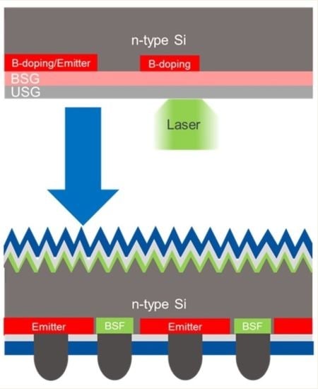
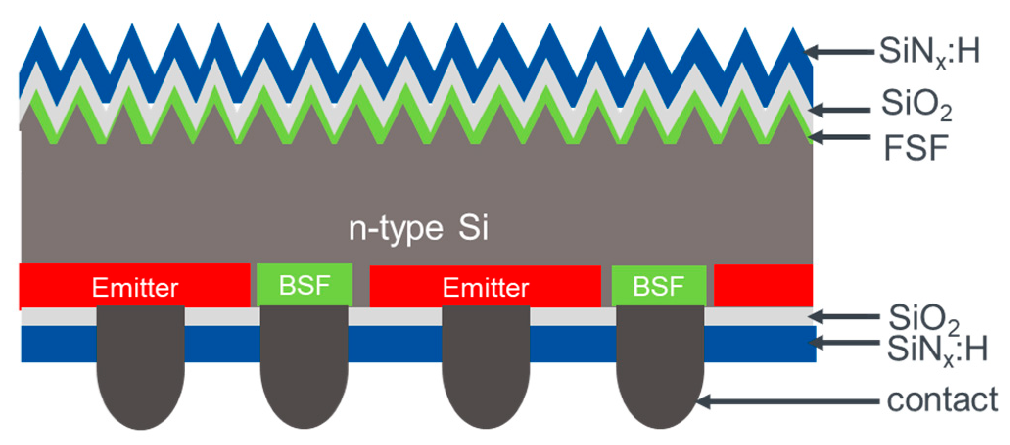
2.1. Solar Cells

In our experiments, we used commercially available Czochralski (Cz) grown n-type silicon wafers with a base resistivity p ≈ 1.5 Ωcm and an (100)-oriented surface. The pseudo-square wafers of size M2 (edge length of the square is 156.7 mm) and an area of 244.3 cm2 had a thickness of around 140 µm after texturing and polishing. The front side of the wafers used for solar cells was chemically textured with a potassium hydroxide and Alkatex solution to obtain random pyramids. The Alkatex solution was commercially available. The rear side of the wafers for solar cells and the test samples for lifetime were chemically polished, also with a potassium hydroxide solution at a temperature of 80 °C.
Figure 1 schematically shows the cross section of the Laser-IBC solar cells. After texturing the front and chemically polishing the back side, further processing began with the one-sided deposition of boron-containing precursor layers by APCVD: Borosilicate Glass (BSG) and the capping layer of Undoped Silicate Glass (USG). Then, local laser doping created the locally well-defined boron-doped emitters on the rear side of the wafer. Thus, the local pn-junctions formed. Then, hydrofluoric acid was used to clean the silicon surface of the remaining precursor. Subsequent RCA cleaning [15] removed impurities before furnace diffusion by phosphor oxychloride (POCl3). This diffusion (in particular the P-content of the phosporusoxide) was co-optimized for the next step of creating the lightly doped front surface field (FSF) [16] and the heavily laser-doped base contact (back surface field, BSF). The P-containing BSF was also locally formed by laser doping between the B-emitter regions, using the furnace-deposited phosphorsilicate glass (PSG) as a P-source. Then, an HF-Dip was used to remove the rest of the PSG. A subsequent, tailored etch-back with a solution of hydrofluoric acid, nitric acid, and acetic acid uniformly etched the high surface concentration of phosphorus at the silicon surfaces at a depth of around 50 nm. This shallow etching step only removed a small fraction of the deep doping profile of the (more deeply laser-diffused) BSF as well as the boron-emitter, also increasing the parallel resistance of the finished cells. The texture on the front side was not affected, while the sheet resistance of the FSF increased slightly. Another RCA-step was employed to clean the sample before the next step of dry thermal oxidation. A double-layer stack consisting of a thermally grown 15 nm thick silicon dioxide (SiO2) together with 65 nm thick plasma-enhanced chemical vapor-deposited silicon nitride (SiNx:H) passivated the front and rear side. Finally, screen-printed, dried and fired silver paste came into contact with the emitter and BSF regions. The four busbars for each polarity were separately printed with a low-temperature, cured silver paste and were isolated to the contact fingers of opposite polarity via a printed and cured polymer paste. The metallization design resembles that of ZEBRA cells [17,18] and allows for bifacial illumination.
Current/voltage-measurements of the IBC cells were performed using a cell flasher from HALM, based on the Cetis PV-CT-L1 tool.

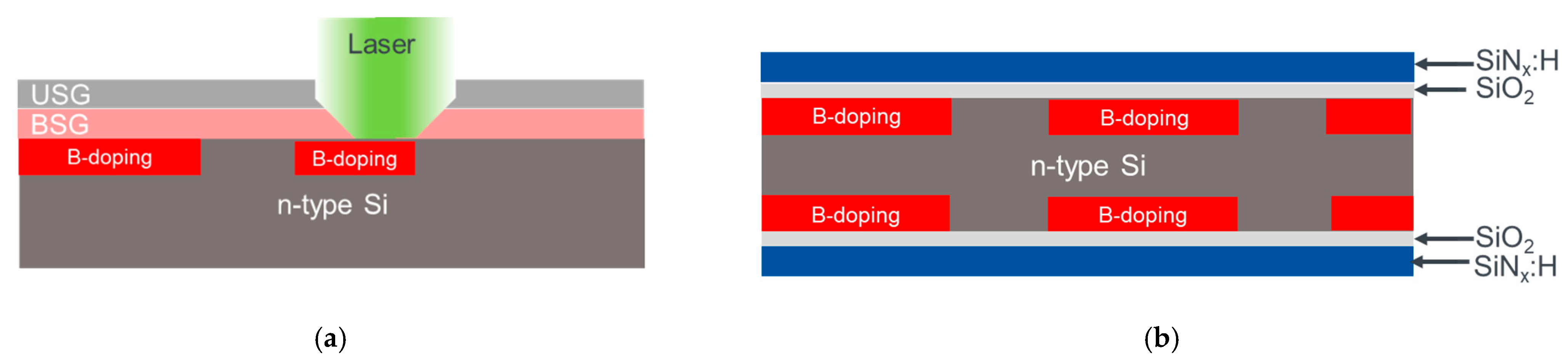
2.2. Structure of Test Samples

During solar-cell processing, we monitored different steps by measuring specifically designed test samples. The laser doping of boron out of the APCVD-layers was analyzed using control samples and by measuring the following aspects:
  • Sheet resistance Rsh;
  • Lifetime τ;
  • Saturation current density J0;
  • Contact resistivity ρc.
Figure 2a shows a schematic cross section of the Rsh-sample, while the cross section of the τ-sample is presented in Figure 2b. After the deposition of the APCVD-layers BSG and USG, the laser irradiated the precursor with different laser pulse energy densities (see Section 2.3).
The passivation of the front and the rear side of lifetime samples consists of the same stack used in the passivation of solar cells (see Section 2.1). The Rsh-values were measured with a four-point-probe and checked using the Transfer Length method (TLM) at contact resistance samples, both methods used the set-up GP Solar GP 4-Test Pro. The lifetimes τ derived from a quasi-steady-state photo conductance measured with a Sinton WCT-120 that, in turn, yielded the saturation current density J0 [19].
For the characterization of Rsh, the laser irradiated fields with an area of 1.5 × 1.5 cm2. Including one field without doping, there were 15 laser doped fields on the wafer with different laser parameters. For characterization of the lifetime τ, the laser irradiated eight fields symmetrically on both sides of the wafer with a size of 4.0 × 4.0 cm2, resulting in eight laser doped fields and one without laser doping. The contact resistivity was measured on fields irradiated by the laser with different laser pulse energy densities similar to the τ-samples in areas of 4.0 × 4.0 cm2. After passivation and metallization with the silver fingers (see Section 2.1) and cutting into strips of 1 cm width, TLM was used to measure the contact resistivity.

2.3. Laser Doping Set-Up

The setup for laser doping included a Q-switched frequency-doubled Nd:YAG laser with a wavelength λ = 532 nm and a pulsed laser beam with pulse duration τp between 41 ns < τp < 110 ns at full-width-half-maximum intensity. Optics formed a quasi-line focus with a width of 12 µm in the x-direction and a length of 280 µm in the y-direction. The laser intensity I, along the short (x-)axis had a Gaussian distribution and a top-hat distribution along the long (y-)axis. The laser pulse energy density Hp was calculated according to Hassan et al. [20]. To dope large areas, the laser irradiated the sample by scanning in the x- and y-direction and by moving a table on which the sample was mounted. As a consequence, the laser pulses overlapped in the x-direction with Ox und in the y-direction with Oy. Both overlaps are represented as a percentage of the whole width of a single laser beam.
The laser doping itself relied on liquid-phase diffusion in the molten Si. On the one hand, the several-nanoseconds-long laser pulse led to the melting of the Si for about 100 ns. On the other hand, the laser pulse also evaporated the APCVD-deposited precursor. The resulting re-condensed vapor of the precursor served as the source for the doping process [20,21]. In molten Si, the dopants’ diffusion coefficient was orders of magnitude higher compared to the solid state [22].

2.4. Deposition of APCVD-Layers

When compared to furnace diffusion, the APCVD process has the advantage of resulting only in a one-sided deposition. Additionally, deposition is possible without the evacuation of the process chamber. This leads to a more cost- and time-efficient process in comparison to sputtering or evaporation processes [23].
In our experiments, we used the APCVD-lab-tool “SierraTherm 5K6-130C56-13-BSG/PSG-SITiO2” from the company SCHMID. The wafers were transported by a metallic belt, first into a heating zone, then through three injection chambers and, finally, through a cooling zone. In contrast to the lab tool with a metallic belt, the industrial tools of SCHMID use a belt with ceramic parts. Those metal-free industrial tools were not available to us at the time of our investigation.
In the first chamber, BSG deposition occurs by the injection of diborane (B2H6), silane (SiH4) and oxygen (O2) [24] gases and the following chemical reaction:
SiH 4 + 2 O 2   SiO 2 + 2 H 2 O
The B2H6 reacts with O2 by
B 2 H 6 + 3 O 2   B 2 O 3 + 3 H 2 O
Chambers 1, 2 and 3 contained the same injection heads, whereas chambers 2 and 3 were used for the deposition of undoped silicate glass (USG) by the reaction of the gases SiH4 and O2. The effective wafer temperature was 360 °C for the deposition of BSG and around 400 °C for USG. The purity of the gases was around 5 N. The concentration of boron in BSG was controlled by the injection of 5% diborane in hydrogen and silane and the ratio of these gases. All of the boron from the gas was incorporated into the BSG-layer, as confirmed by glow discharge optical mass spectrometry. Ellipsometry measurements were used to control the thickness of the layer.
Unfortunately, the transportation belt of the lab-type APCVD reactor is made out of metal, which provides advantages in terms of the versatility of the system to deposit, alongside doped glasses, TiO2, AlOx, and in situ doped aSi/polySi. Industrial-type transport systems for the wafers use pure ceramic rolls. In order to avoid the metal contamination of wafers and the APCVD-layers using the metal belt system, we tested different support wafers in the experiments, which served not only as wafer carriers but also as diffusion barriers between the metallic belt and the solar cell wafers (see Section 3.2 and Section 3.4). At the deposition temperatures used, metals out of the belt were able to diffuse into the solar cell wafers and also into the APCVD-layers. To minimize possible contamination further, the metal belt was coated with BSG and USG for several hours to build an even more effective diffusion barrier. Nevertheless, when using the metal belt, contamination of the APCVD-layers cannot be avoided completely. Therefore, we tested different support wafers as diffusion barriers between the belt and the test samples (see Section 3.2). For each deposition run, we used cleaned support wafers, that had been partly used multiple times, for deposition on both sides of the wafers. Dipping with hydrofluoric acid directly before deposition as well as RCA cleaning ensured that the Si surface of the test samples was clean before being sent to SCHMID. The wafers were exchanged between ipv and SCHMID by mail via nitrogen-containing packages.

3. Results

In the following Section, we show that the APCVD-layers are well suited for laser doping the pn-junction for solar cells and—despite the metal conveyer in the APCVD system—we reached efficiencies of above 22.5% with a maximal value of 23%. For this purpose, we compared the following three different processes for fabricating the pn-junctions on the n-type solar cell wafers: (i) laser doping via sputtered boron oxide layers leading to 23.2% [11], (ii) laser doping via APCVD-layers, and (iii) furnace diffusion of boron by boron tribromide (BBr3) yielding 23.3% efficient cells.

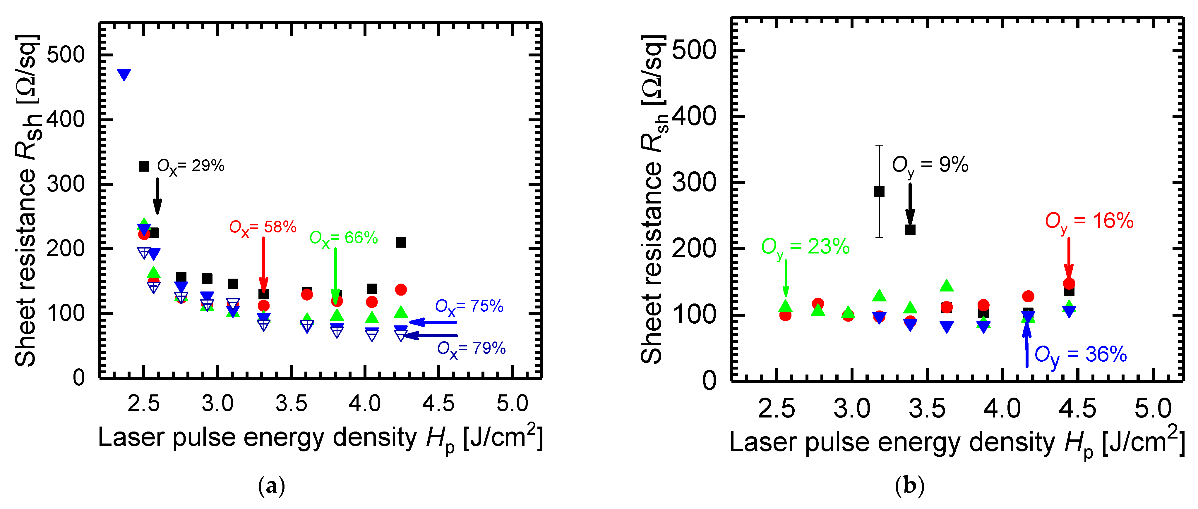
3.1. Laser Doping and Sheet Resistance

The success of laser doping of Si highly depends on the composition of the precursor. The BSG layers tested here with capping layers of either USG or aSi are characterized as follows:
  • Boron concentration CB within the BSG;
  • Thickness dBSG of the BSG;
  • Thickness dUSG of the capping layer USG, or daSi of aSi.
The capping layer of either aSi or USG prevents the chemical reaction of B2O3 with humidity (from the air) to boric acid.
The measured sheet resistance Rsh of the boron-doped layers was used to investigate the correlation of the laser irradiation and the composition of the layers as a function of the laser pulse energy density Hp and laser pulse overlap O.

3.1.1. Laser Pulse Overlap

The pulse energy density Hp of the laser changes the melting depth of the Si, while the overlap O, controls the doping profile [20]. Therefore, the sheet resistance as well as the doping profile can be tailored with proper laser parameters [20,21,22].
Figure 3a shows the optimization of the overlap Ox for 29% < Ox < 79% while the overlap in the y-direction Oy remains constant Oy = 12.5%. The APCVD layers for these experiments consisted of a BSG layer of a thickness of dBSG = 40 nm with 12% boron and a USG layer of a thickness of dUSG = 20 nm. At 75% < Ox < 79%, the sheet resistance Rsh leveled off at Rsh,min ≈ 70 Ω/sq. Figure 3b shows the resulting Rsh with a variation of Oy in the range 9% < Oy < 36%. For the variation, we increased the thickness of USG to dUSG = 40 nm and decreased the boron concentration in BSG to CB = 8%. Only the value of Oy ≤ 9% seemed to influence Rsh at different laser-pulse-energy densities Hp. With these results, we proceeded with Ox = 75% and Oy = 13% as the standard for further laser doping.

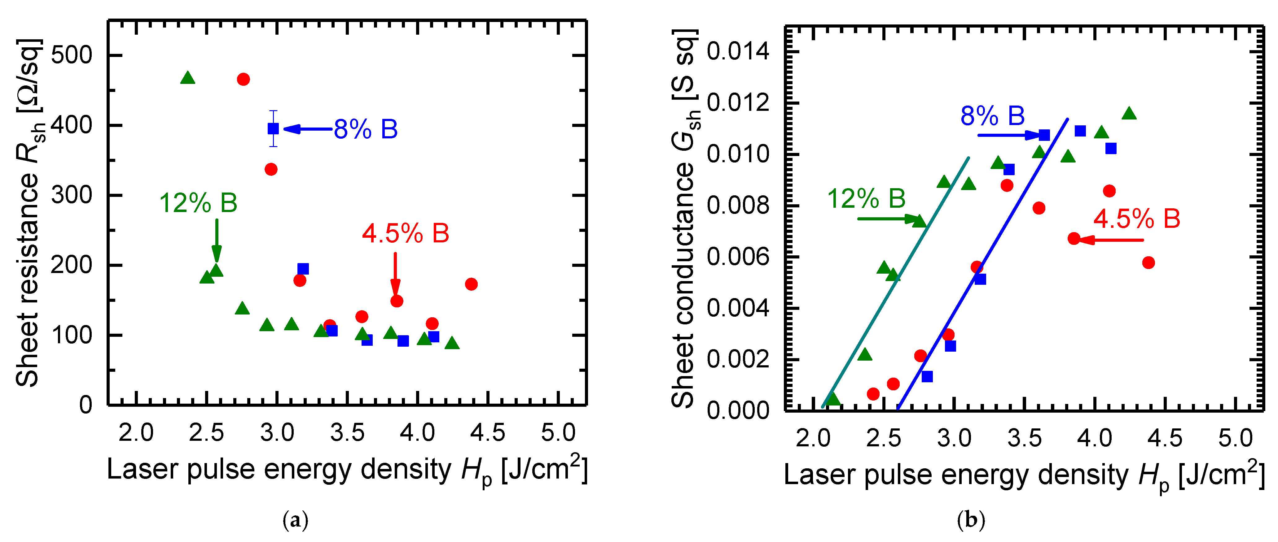
3.1.2. Boron Concentration

The boron concentration CB in the BSG controls the maximum possible doping concentration CB,em of the p-type layer of the pn-junction. For our APCVD parameters, the maximal possible B-concentration in the BSG was CB = 12%. We used CB,1 = 4.5%, CB,2 = 8%, and CB,3 = 12% for dBSG = 40 nm and dUSG = 20 nm for different laser-pulse-energy densities Hp.
Figure 4a shows the Rsh after laser doping of APCVD-layers with a BSG of thickness dBSG = 40 nm and USG with dUSG = 20 nm. Stable and leveled-off sheet resistances Rsh ≈ 80 Ω/sq were reached between 3 J/cm2 < Hp < 4 J/cm2 for a boron concentration of CB,3 = 12% of the APCVD layers. The lower CB,2 = 8% required a higher Hp for the same Rsh, while CB,1 = 4.5% did not result in stable Rsh. We found that the higher the CB, the lower the threshold in Hp for a given value in Rsh. This correlation is shown in Figure 4b where—instead of Rsh—the equivalent sheet conductance Gsh = 1/Rsh is plotted. Laser doping requires laser energies Hp of above the melting threshold Hp,thres of the Si [20]. The doping threshold was observed via an increase in the sheet conductance in Figure 4b. Due to the partial absorption of the laser power within the APCVD-layer, the measured threshold was found to be dependent on the boron content of the precursor layer. With Hp,thres,3 (12%) = 2.1 J/cm2 in Figure 4b, the threshold energy Hp,thres for laser doping with CB,3 = 12% was found to be lower than Hp,thres,2 (8%) = 2.6 J/cm2 for CB,2 = 8%. This is discussed in more detail below.

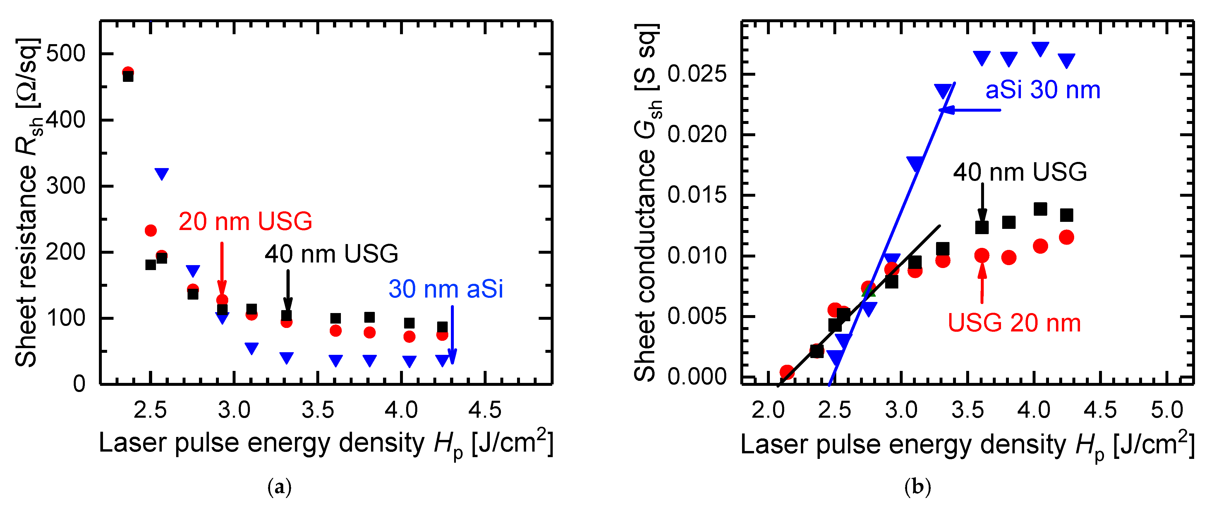
3.1.3. Variation of Capping Layer

The APCVD equipment provided the opportunity to deposit, as the capping layer, amorphous Si (aSi) instead of USG. Hence, we compared the laser doping from BSG with different capping layers of USG with thicknesses of (i) dUSG,1 = 20 nm and (ii) dUSG,2 = 40 nm, and finally, also with aSi capping (iii) with a thickness of daSi = 30 nm. The BSG had a boron concentration of CB = 12% and a thickness of dBSG = 40 nm.
Figure 5a shows the sheet resistances Rsh after laser doping. The main result is that the thickness of the USG did not influences Rsh at Hp < 3.3 J/cm2; therefore, the thicker the USG, the higher the Rsh at Hp > 3.3 J/cm2. The aSi capping layer yielded the lowest Rsh. With the sheet conductance values in Figure 5b, we can derive the threshold values Hp,thres for the laser doping. The Hp,thres are about the same for dUSG,1 = 20 nm and dUSG,2 = 40 nm, whereas they are higher for the aSi-capping Hp,thres,aSi > Hp,thres,USG. The lower band gap of the aSi layer absorbs more laser radiation than the USG. Therefore, it required more power to melt the underlying Si and to evaporate the BSG layer.
At first sight, the aSi capping layer seems more attractive than USG. However, the aSi capping layers lead to a severe processing problem, in that after the laser doping, the surface cannot be cleaned completely, as shown in Figure 6. Neither cleaning with a KOH solution nor with a solution of hydrofluoric acid, nitric acid, and acidic acid results in clean surfaces without rests or glitters. Therefore, we did not continue experiments with aSi capping layers. However, as the deposited aSi layers were in situ boron-doped, a BRL (boron rich layer) could have been formed during laser processing, complicating and partially preventing etching.

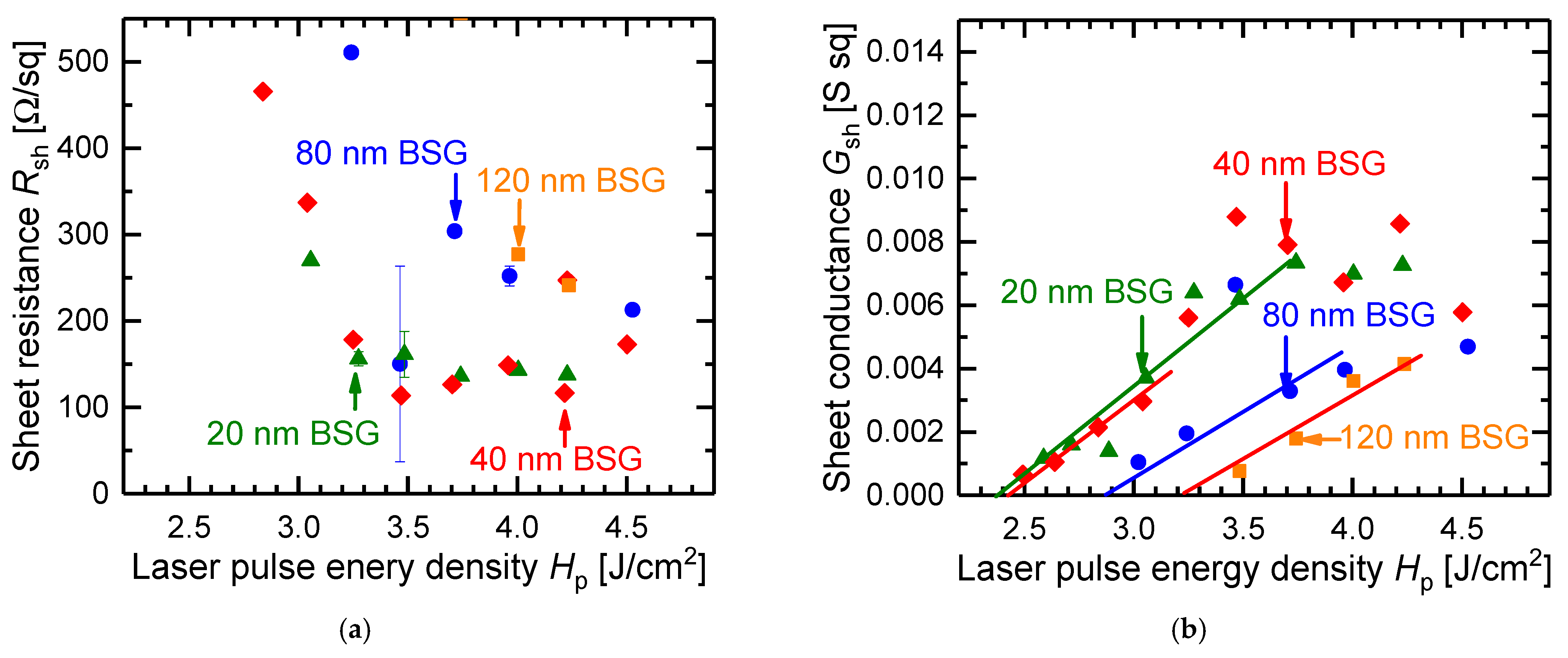
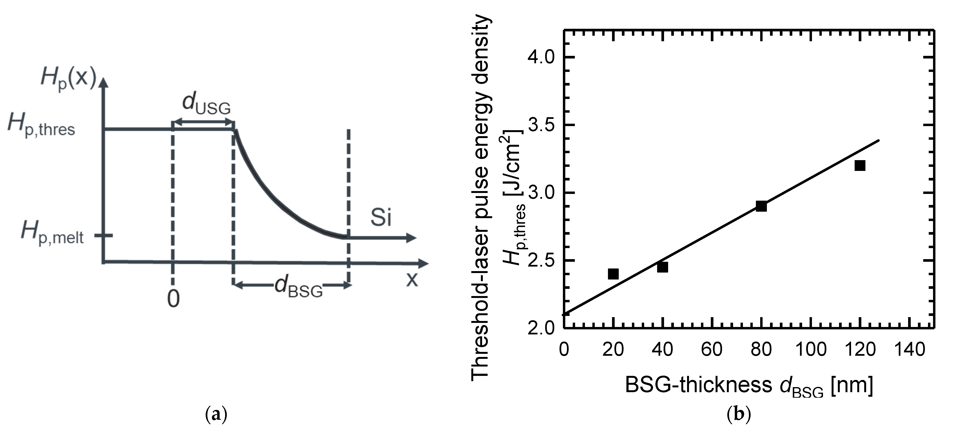
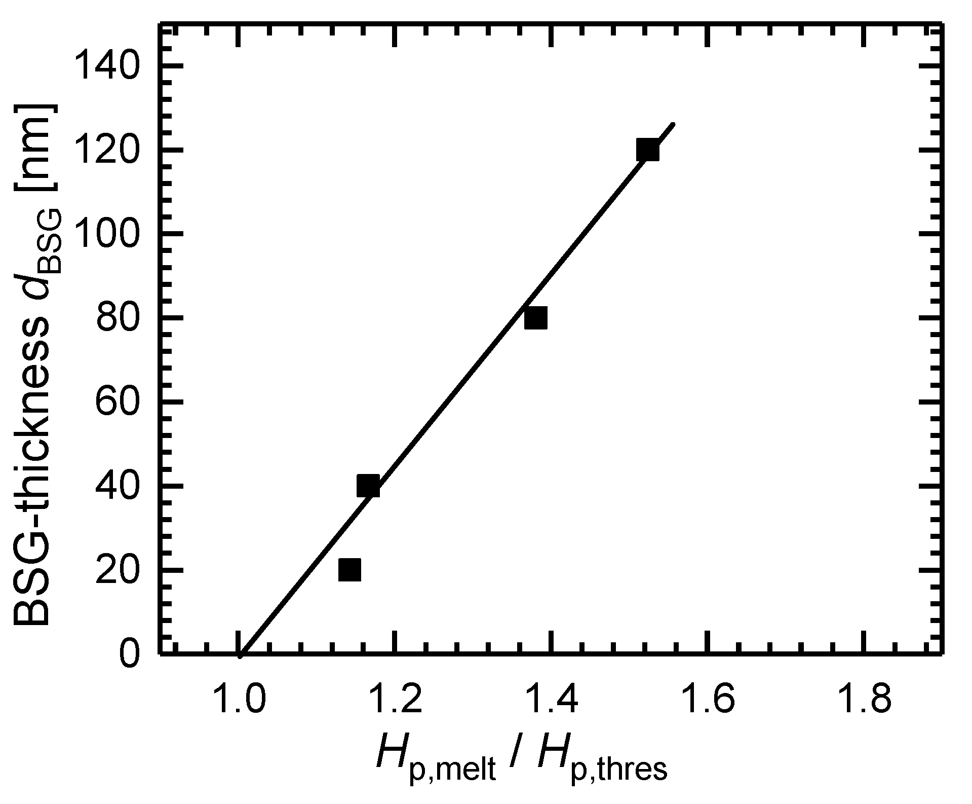
3.1.4. Thickness of BSG

For a fixed boron content in the capping layer, different thicknesses led to the following two effects: on the one hand, the thicker the layer, the more boron atoms available for laser doping. As a result, the final doping concentration in the boron emitter of the solar cell increased. On the other hand, thicker BSG layers led to a stronger absorption of the laser beam. Therefore, more power is needed to melt the underlying Si for doping. The required threshold value was higher. In our experiments, we varied the BSG thickness dBSG in the range of 20 nm < dBSG < 120 nm, while the boron concentration CB = 12% and the thickness dUSG = 40 nm of the USG capping layer remained constant.
Figure 7a shows Rsh after laser doping with different laser-pulse-energy densities Hp. The Rsh values are about the same for BSG with dBSG,1 = 20 nm and dBSG,2 = 40 nm. In contrast, dBSG,3 = 80 nm and dBSG,4 = 120 nm require higher Hp. Figure 7b allows us to deduce the threshold values for laser doping from the values for Gsh  0 S sq. These threshold values Hp,thres increase with the thickness dBSG of the BSG-layer and are:
  • Hp,thres,1 = 2.4 J/cm2 for dBSG,1 = 20 nm;
  • Hp,thres,2 = 2.45 J/cm2 for dBSG,2 = 40 nm;
  • Hp,thres,3 = 2.9 J/cm2 for dBSG,3 = 80 nm;
  • Hp,thres,4 = 3.2 J/cm2 for dBSG,4 = 120 nm.

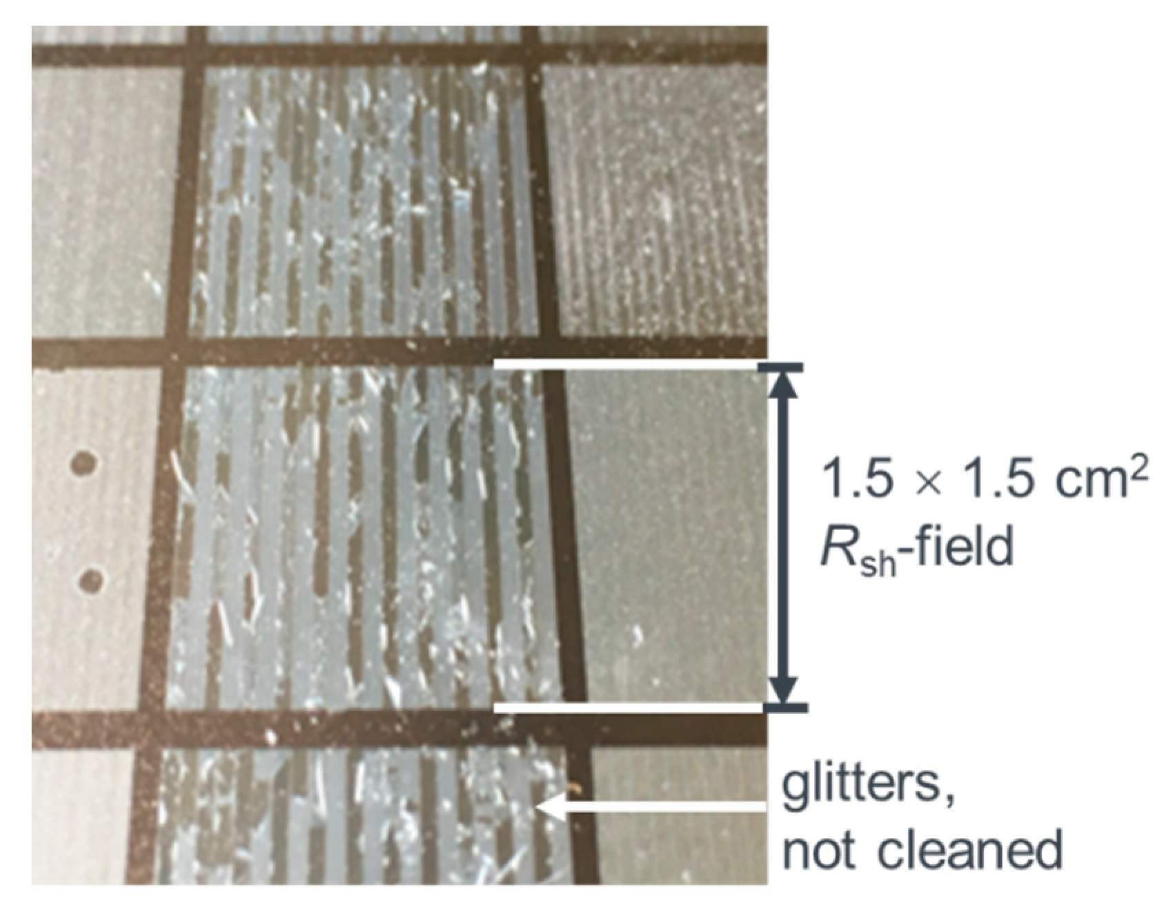
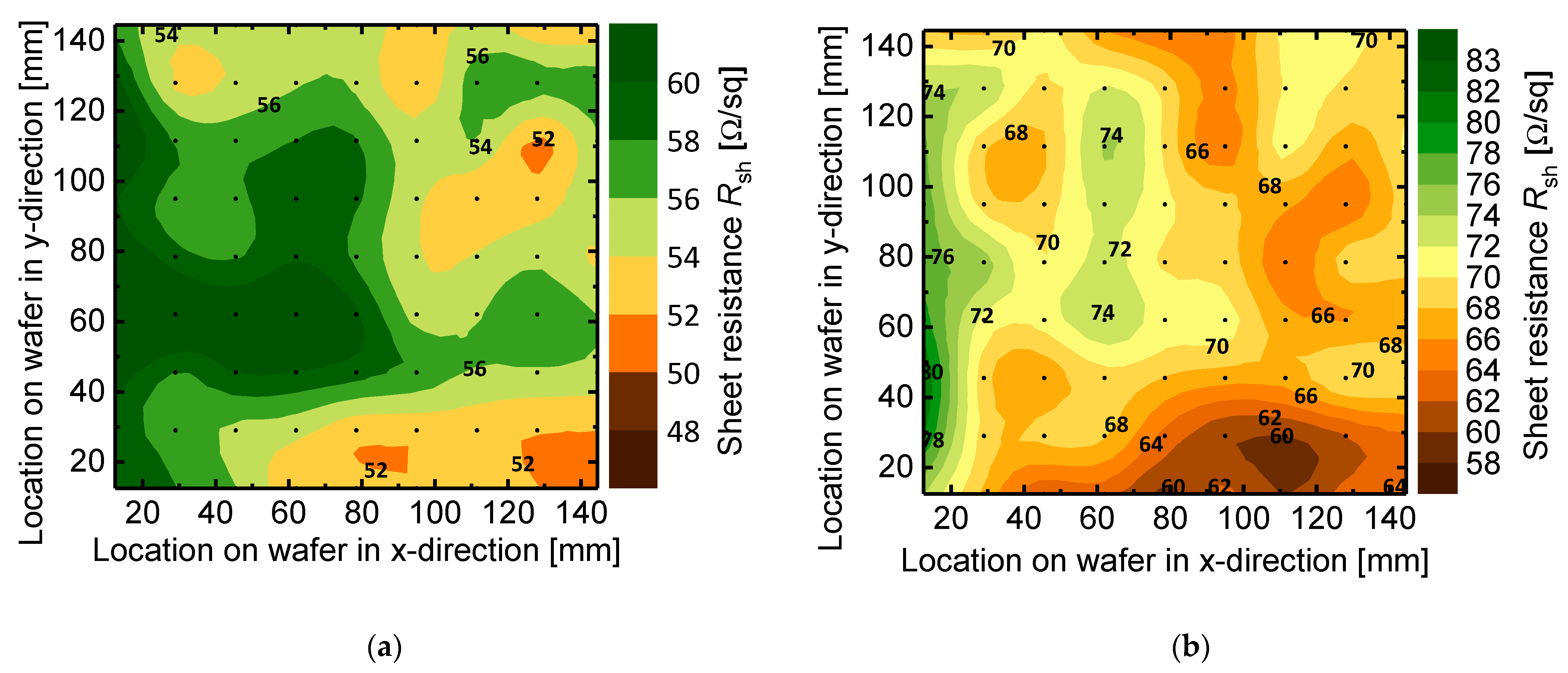
3.1.5. Homogeneity of APCVD-Layers

To obtain more information about the homogeneity of laser-doped pn-junctions for solar cells on the area of M2-wafers, we laser-irradiate the full area of the Si wafers with BSG/USG on top with one laser pulse energy density, of Hp = 3.6 J/cm2. The key parameter for the laser doping of thin layers is the thickness of the layer and the content of the doping material. The Rsh measurements were performed on 81 points, evenly distributed over the wafer.
Figure 8a shows the color contour plot of Rsh after laser doping of the APCVD-layer with BSG of thickness dBSG = 40 nm and boron concentration CB = 12% and USG with a thickness dUSG = 20 nm. The mean value is Rsh,mean = 59 Ω/sq with a difference of ΔRsh = 10 Ω/sq between the maximal and minimal value. After laser doping the pn-junction for solar cell processing, phosphorus diffusion occurred for the BSF field and the growth of thermal silicon dioxide (for the surface passivation). Figure 8b displays the changed Rsh. We obtained a mean value of Rsh,mean,ox = 69 Ω/sq and a deviation of ΔRsh,ox = 20 Ω/sq. The etchback after P-diffusion and oxidation increased the Rsh.

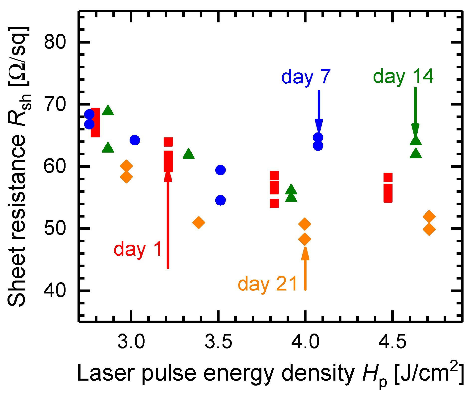
3.1.6. Stability of APCVD-Layers

Figure 9 shows the stability of the APCVD layers for laser doping. The layers consisted of BSG with a thickness of dBSG = 40 nm, a boron concentration of CB = 12%, and USG of dUSG = 20 nm. Four laser-doping experiments were performed over the course of 21 days in order to investigate the effect of storing the APCVD layers before the laser-doping process. Before laser doping, the wafers with the layers were stored in a nitrogen atmosphere to protect them from air humidity. Only a minimal variation in the range of 10 Ω/sq < ΔRsh < 15 Ω/sq was observed within this time.

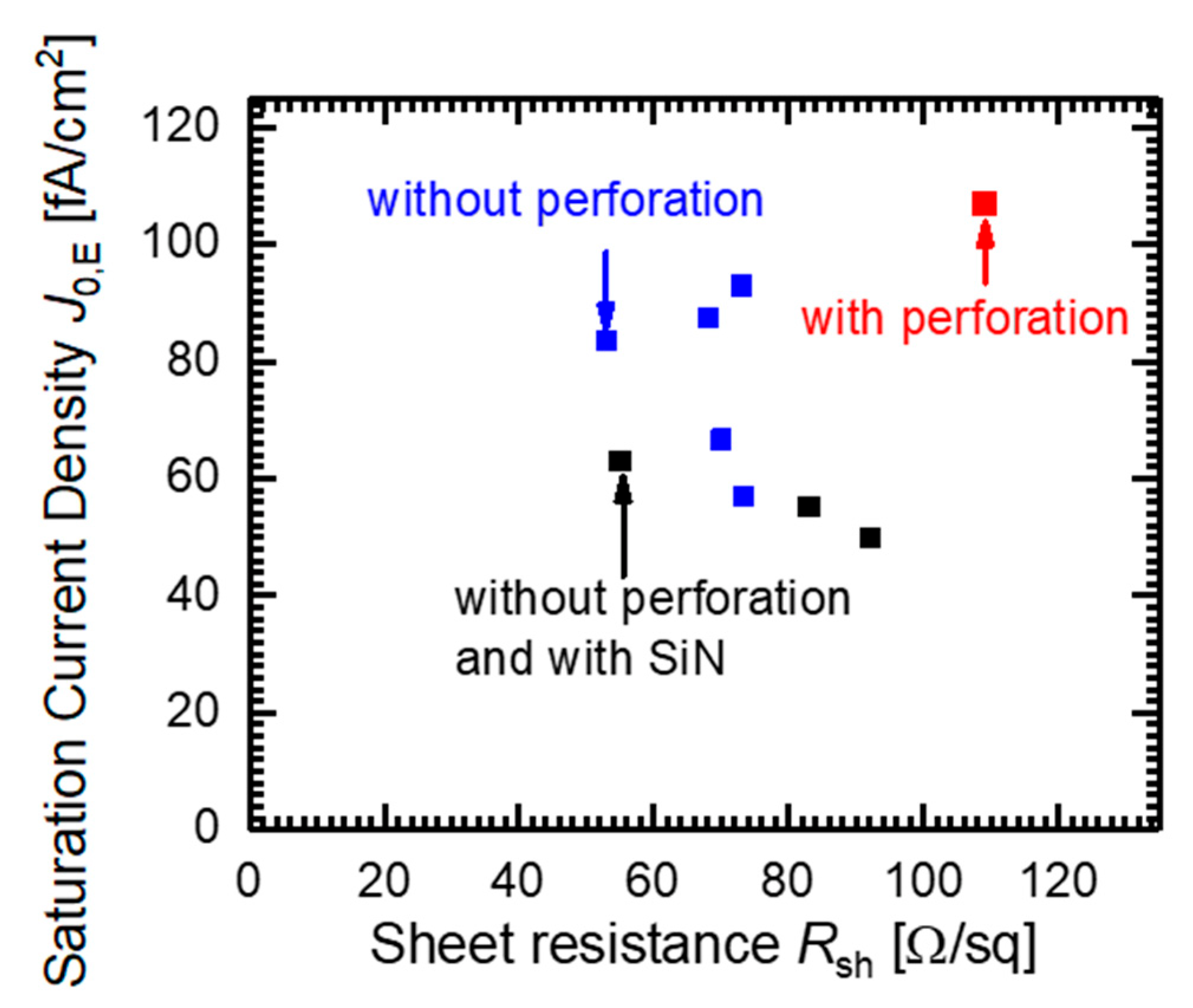
3.2. Saturation Current Densities

During deposition of the APCVD-layers, the wafers were transported on support wafers to avoid possible contamination from the metallic belt of the conveyer. As support wafers, we used M2-sized Cz-Si wafers with a texture on both sides. The APCVD layers consisted of BSG with a thickness of dBSG = 40 nm, a boron concentration of CB = 12%, and USG with dUSG = 20 nm. The sheet resistance varied due to different laser-pulse-energy densities.
We tested the following support/diffusion barrier wafers (SW) between the metal belt and the process wafers:
  • Unperforated wafers with 200 nm thick SiN deposited on both sides;
  • Perforated wafers to avoid floating of the wafers during APCVD depositions (“perforation” means small holes in the wafer);
  • Unperforated wafers.
To understand its influence on the purity of the APCVD-layers, we measure the effective lifetime τeff and extracted the saturation current density J0,E after laser doping and the passivation of the surface (see Section 2.2). The corrections of τeff due to Auger- and radiative recombination in the bulk in the form of the intrinsic lifetime τintr and the injection-corrected intrinsic-carrier density ni,eff were included in the software of the WCT-120 tool. The Auger- and radiative corrected lifetime τcorr can be described by
1 τ corr = 1 τ eff 1 τ intr = J 0 , E N b + n q w n i , eff 2    
showing the influence of the bulk doping Nb, the concentration of injected charge carriers Δn, the width w of the sample, and the elementary charge q [25,26]. When measuring τeff at a high injection, the lowly doped base enters into high-injection, while the highly doped emitter remains in low-injection. In the high-injection state, the Shockley–Read–Hall (SRH) lifetime of the bulk Si is assumed to be higher than τintr and higher than the lifetime in the highly doped emitter or not injection dependent [27,28]. From the derivative of 1/τcorr with respect to Δn, we were then able to extract the J0,E via the following equation
d d Δ n   1 τ corr   = 2 J 0 , E q w   n i , eff 2  
As result, Figure 10 shows the J0,E for the case of using the support wafers during APCVD-deposition. The lowest J0,E is reached with the support wafers (SW) without perforation and with SiN. Unfortunately, the deposition with the SW with perforation exhibits only one value of J0,E = 110 fA/cm2, the highest J0,E of all. Metallic impurities from the transport belt probably reached the process wafers via the holes in the SW. The J0,E with deposition on SWs without perforation ranges from 58 to 94 fA/cm2. Only the deposition on SWs without perforation and with SiN resulted in a decreasing J0,E with increasing Rsh (lower doping); with the lowest J0,E = 40 fA/cm2 at Rsh = 104 Ω/sq. Only the J0,E of the test samples with the deposition on SW without perforation and with SiN show a dependence on Rsh. The decrease in J0,E with increasing Rsh suggests that lifetime is limited more or less by the Auger-recombination in the emitter and not by contaminations or defects. The lifetime due to Auger-recombination should show a dependence on the inverse of the square of the charge carrier concentration of the highly doped emitter [29] or, in other words, it should increase with Rsh2 or vice versa to J0,E.
If the APCVD-process contaminated the BSG/USG-layer, the laser doping would bring the contamination into the emitter within a depth of around 1 µm [20]. The etch-back following P-diffusion (see Section 2.1) also ensures at least a partial removal of contaminants on the surface.
Parallel to the samples shown here for measuring lifetime/saturation current density, we processed solar cells with emitters from the deposition of APCVD layers with SW without perforation and with SiN and laser doping—see the following Section 3.4.

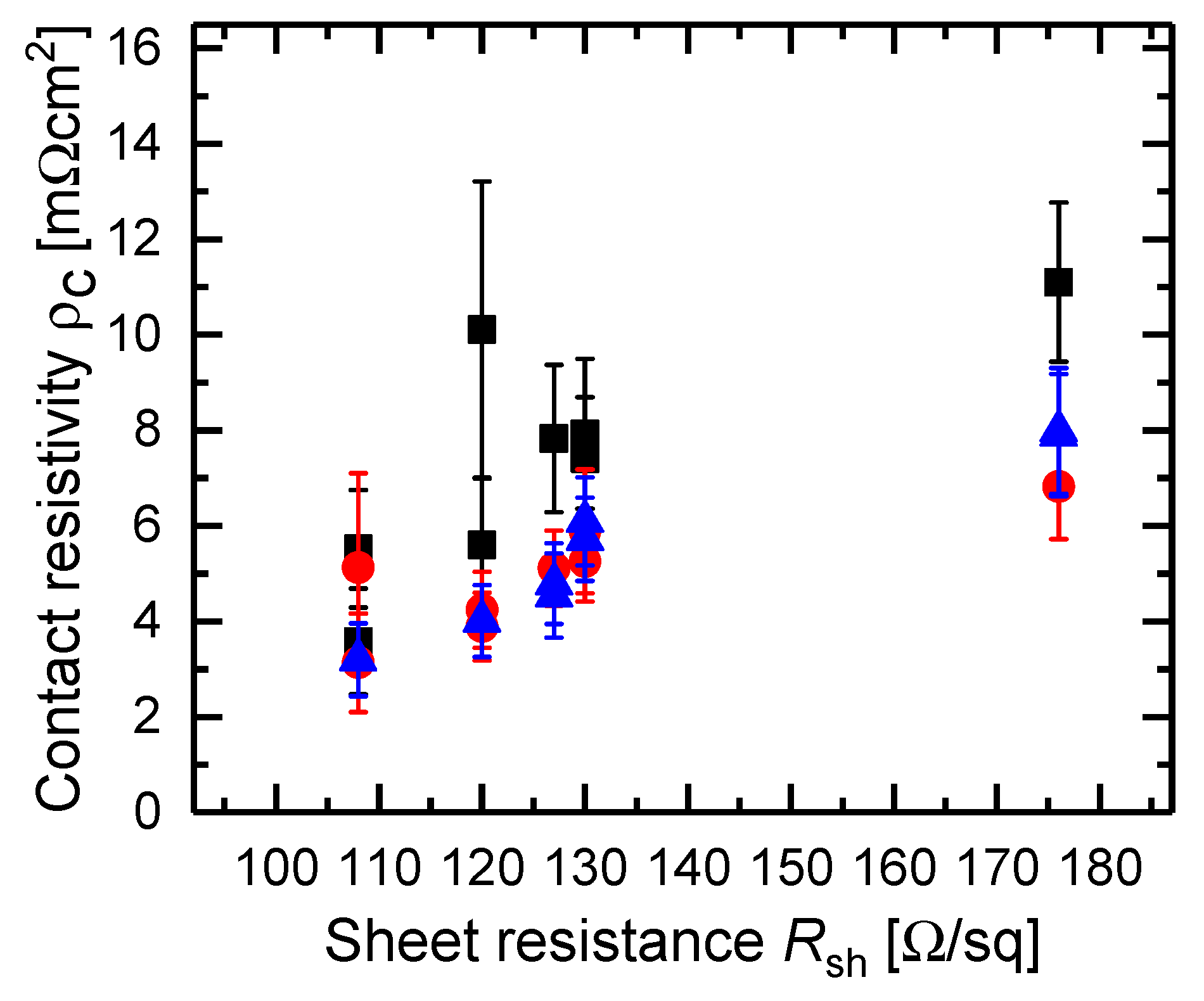
3.3. Contact Resistivity

High quality Ohmic contacts on the boron-containing laser-doped emitters of our cells required low contact resistances ρC to the screen-printed silver paste. Figure 11 shows the ρC of the fired Ag paste on the laser-doped APCVD layers. The ρC decreased with decreasing Rsh, with the lowest ρC = 3 mΩcm2 at Rsh ≈ 108 Ω/sq. The APCVD-layers consist of BSG with a thickness of dBSG = 40 nm, a boron concentration of CB = 12%, and USG of dUSG = 20 nm. Sheet resistance varied due to different laser-pulse-energy densities.

3.4. Solar Cell Results

The saturation current density J0,E of the pn-junction influences the electrical characteristics of the solar cell, mainly in terms of the open circuit voltage and therefore, also the efficiency. Clearly, other parameters also have an influence, but they are not considered here. Figure 12 shows the influence of the achieved J0,E on the maximum efficiency of the solar cells by using the support wafers without/with perforation, and without perforation but with SiN. The J0,E was measured on test samples, while solar cells were processed in parallel with the same emitter. The solar cell batches consisted of 10 to 20 cells.
Figure 12a provides the maximum open circuit voltages Voc,max achieved, while Figure 12b presents the maximum efficiencies ηmax achieved. The highest Voc,max and ηmax are coupled with the transport by wafers without perforation and with SiN resulting in Voc,max = 690.7 mV and ηmax = 23%—see also Table 1 for the batch with the emitter made of BSG/USG.
With these findings, we processed solar cells with an emitter made of an APCVD layer with a boron concentration of 12%, a thickness of BSG of 40 nm and a thickness of USG of 20 nm, which we deposited on support wafers without perforation and with SiN. Table 1 presents the electrical solar cell parameters of the different batches of solar cells, as follows: efficiencies η with their mean value and standard deviation in the cell batch, maximum achieved efficiency ηmax, short circuit current density Jsc, open circuit voltage Voc, and fill factor FF. The table also compares different processes for boron-emitter formation, including (i) boron laser doping from sputtered boron oxide [16], (ii) boron laser doping from APCVD-layers with BSG and USG, and (iii) the furnace diffusion of boron. Unfortunately, our sputtering equipment did not produce homogeneous boron oxide layers over a large area. Therefore, the cell size for this process was limited to an area Acell = 4 cm2. Additionally, in contrast to the large area cells Acell = 244.3 cm2, these small cells did not have screen-printed contacts, but used evaporated aluminium contacts. Table 1 shows that—despite the problem of possible contamination from the metallic belt of the conveyer in the APCVD reactor—the large-area, screen-printed cells with a maximum value of 23% reached close even to our previous best, small-area cells with 23.2% efficiency. Additionally, the results agree with previous data of cells made with the furnace-diffused boron emitter with efficiencies of 23.3%. Therefore, with a high probability, cells with a boron precursor from a commercial APCVD reactor with a ceramic roller transport system might also reach 23.3% if the emitter reaches similar J0E-values such as the J0E,diff < 40 fA/cm2 achieved with boron-furnace diffusion. In addition, the overall contact design—which is close to the (old) ZEBRA design of the ISC Konstanz is being reconsidered. The current metallization design used only four bus bars for each polarity on the back side of these cells. Using more busbars would reduce the finger width of the contact fingers and increase the fill factor of the cells.
We also measured the bifaciality of the IBC cells on the module level—see Appendix B. Two modules were assembled out of 120 IBC half cells. The calculation of the bifaciality B according to equation B1 yields B ≈ 70%. With a similar metallization scheme, Mihailetchi et al. [30] showed a bifaciality of B = 67% on the cell level and of B = 70% on the module level.

4. Absorption in the Precursor Layer

Tailoring the boron-laser doped emitter requires control of the following aspects:
  • Boron concentration CB of in the BSG;
  • Thickness dBSG of the BSG as the source for laser doping;
  • Thickness dUSG of the protecting USG-cap.
Next, we estimated the influence of absorption and reflection in the precursor layer from the results of laser doping (see Section 3.1.4) with the simplification of neglecting interference effects. For laser doping, the laser pulse energy density Hp has to be high enough to melt the Si. Figure 5b and Figure 7b show that the threshold value Hp,thres depends on the thickness of the BSG layer. This effect is simply due to the absorption in and also reflection of the BSG and (if too thick) also the USG cap. Doping takes place only if the underlying Si layer melts. Below the threshold energy density, the (parasitic absorption) of the laser pulse in the BSG/USG simply evaporates or ablates the BSG/USG stack but does not yet melt the Si. The data in Figure 5b show that there is no difference in the data for the 20 and 40 nm thick USG layer. Therefore, we neglected the absorption of the laser pulse within these USG layer. Moreover, we ascribed the different threshold values from the data in Figure 7b to parasitic absorption and reflection in the BSG, where the measured threshold energy is higher, because not all of the laser power (and energy) reaches the interface between the BSG and the silicon wafer.
Figure 13a shows the decrease in the laser energy as it passes through the BSG layer. The incident laser energy, if equal to the (measured) threshold energy Hp,thres, must increase to reach the energy Hp,melt which is necessary to melt the Si. From Lambert-Beer’s absorption law, we find
Hp,melt (dBSG) = (1 − R) Hp,thres (1 − exp(−dBSG/Lα))
where Lα stands for the absorption length of the green laser beam within the BSG and R for the reflection of the BSG/USG-layer on top of the Si (which is not shown in Figure 13a).
For dBSG < Lα, the Taylor expansion of Equation (5) leads to
dBSG = Lα/(1 − R) Hp,melt/Hp,thres
where Hp,melt equals Hp at dBSG = 0 nm (see Equation (5)). As shown in Figure 13b, we can derive an extrapolated value Hp,melt = 2.1 J/cm2 for our laser parameters. This value is in good agreement with our earlier publications [7,8,11,16,20,21] on very thin (around 2 nm) sputtered precursors and supports the assumption that R is approximately independent of the thickness dBSG of the APCVD-deposited layers. Additionally, interference effects in the precursor layer seem to play a minor role.
Finally, Figure 14 plots the thickness of the BSG versus the ratio Hp,melt/Hp,thres. With a measured reflection range of 30% < R < 40% on different BSG/USG-layers (which is roughly the same reflection as for the polished Si-surface with RSi = 37%), the corrected slope of Figure 14 yields an absorption length in the range 330 nm > Lα > 380 nm for the laser wavelength λ = 532 nm. These large values of the absorption length also justify the use of the Taylor expansion in Equation (6).
Our value of an absorption length of around 0.4 µm is surprising because the literature data for silicate glasses indicate low absorption (and therefore higher absorption lengths) in this wavelength regime. However, Kitamura et al. [31] stated in their review that silica glasses differ in their optical properties due to “the silica glass synthesis method, composition, impurity, and defects level, sample thickness, surface roughness, and temperatures as well as the retrieval method”. If we consider the glass-formation temperature of borosilicate glass of around 460 °C [32] and our lower deposition temperatures of 400 °C, we speculate that, in our case, more transparent “glass” had not yet formed. This could explain the difference between the literature data for the absorption of borosilicate glass and the data of our deposited BSG and USG. Additionally, Heilig et al. [14] stated that laser doping from as-deposited (like we did) APCVD layers results in higher doping than laser doping with thermally treated glasses. Clearly, this aspect of laser doping from the APCVD layers deserves more detailed optical study. In particular, a comparison of the optical properties of the APCVD-deposited BSG layers which underwent different thermal treatments requires future investigation. A comparison with BSG-layers from furnace diffusion in future studies will prove interesting. Such basic research was not the primary focus of our present work which concentrated on the basic technologies for processing industrial Laser-IBC solar cells.

5. Conclusions

Boron-containing precursors derived from an APCVD process are well suited for the fabrication of industrial IBC solar cells using laser doping. For large-area cells, we reached an efficiency of up to 23%. According to our experiments with different carrier wafers, this efficiency value is likely to be limited by impurities which, most probably, stem from the metallic belt, which is used in the conveyer system of the lab-type APCVD system. Avoiding this contamination, with the use of, for example, a commercial APCVD system with a ceramic roller-transport system, could lead to an efficiency similar to that of solar cells with furnace-diffused emitters of 23.3%.
For the safe transport of the deposited APCVD layer between different lab locations, a protected nitrogen atmosphere is needed. Under such protection, the precursors can survive for up to three weeks.
In the past, we used only several-nanometer thick, sputtered precursors for boron laser doping IBC solar cells. For such thin layers, the absorption and reflection of the laser beam within the precursor plays no role. The APCVD-deposited layers used here were much thicker. In this case, one must consider parasitic absorption and reflection within the precursor itself. For the green laser beam of a λ = 532 nm wavelength, we observed an absorption length in the range of 380 nm < Lα < 330 nm for the BSG with a boron concentration of 12%.

Author Contributions

Conceptualization, R.Z.-G. and J.H.W.; methodology, R.Z.-G., V.M. and S.F.-R.; validation, R.Z.-G. and T.B.; formal analysis, R.Z.-G. and J.H.W.; investigation, S.F.-R., M.S., E.-P.W. and M.H.; resources, J.K., R.K., J.H.W. and S.S.; data curation, S.F.-R., M.S., E.-P.W., T.B., M.H. and S.S.; writing—original draft preparation, R.Z.-G. and J.H.W.; writing—review and editing, R.Z.-G. and J.H.W.; visualization, R.Z.-G.; supervision, R.Z.-G. and J.H.W.; project administration, R.Z.-G.; funding acquisition, R.Z.-G. and J.H.W. All authors have read and agreed to the published version of the manuscript.

Funding

This work was funded by the German Federal Ministry of Economics and Technology (BMWi) project No. 0324212 and Energy Baden-Württemberg (EnBW).

Informed Consent Statement

Informed consent was obtained from all subjects involved in the study.

Acknowledgments

We thank E. Hoffmann for fruitful discussions during the processing of solar cells and M. Saliba for the opportunity to record the results at ipv and for support in the BMWi project. We also gratefully acknowledge the experimental support of the ipv-technology group under the leadership of B. Winter. We are also grateful for the production and measurements of the solar modules by Ingo Ullmann from ISC Konstanz. Finally, we thank the reviewers for their careful reading of the manuscript which helped to improve our text.

Conflicts of Interest

The authors declare no conflict of interest.

Appendix A

Our in-house measurements, shown in Table 1, were performed with a sun simulator under standard test conditions. Table A1 shows a comparison with the calibration measurements at ISE CalLab on two IBC cells. The values of our in-house measurements are within the error limits of the calibration measurements of ISE CalLab.
Table A1. Electrical parameters of the solar cells calibrated at ISE CalLab in comparison to our in-house measurements at Standard Test Conditions: efficiency η, current density Jsc, open circuit voltage Voc and fill factor FF. Efficiency values of our measurements and from ISE CalLab are in the limit of error.
CellArea
Acell [cm2]
Efficiency
η [%]
Short Circuit Current Density
Jsc [mA/cm2]
Open Circuit Voltage
Voc [mV]
Fill Factor
FF [%]
Cell 1, in-house244.322.441.1682.779.8
Cell 1, ISE244.322.32 ± 0.3440.83682.980
Cell 2, in-house244.322.441.4685.879
Cell 2, ISE244.322.24 ± 0.3441.19684.578.9

Appendix B

The determination of the bifaciality of our IBC cells was performed on the module level. We assembled two modules, each containing 120 half cells. An h.a.l.m. module flasher AAA type with a 1× Xenon lamp cetisPV-CT had the characteristic values of the power PMPP,mod at the maximum power point, efficiency ηmod, short circuit current Isc,mod, open circuit voltage Voc,mod, and fill factor FFmod. Table A2 shows the values of two different modules and the calculated bifaciality.
B = ηmod,rear/ηmod,rear
where ηmod,rear is the efficiency measured with the illumination from the rear side and ηmod,rear is the illumination from the front side of the module. Module 1 shows B1 = 0.692 and module 2 has B2 = 0.724.
Table A2. Electrical parameters of the modules made out of 120 IBC half cells with given mean values out of five measurements and their standard deviation. Illumination occurs either from the front side or the rear side of the modules. The Bifaciality B was calculated using Equation (A1).
ModuleMPP Power
PMPP,mod [W]
Efficiency
ηmod [%]
Short Circuit Current
Isc,mod [A]
Open Circuit Voltage
Voc,mod [V]
Fill Factor
FFmod [%]
Front: Module 1—mean323.419.451042.0376.93
Front Module 1—st. dev.0.11630.00690.00180.00840.035
Rear: Module 1—mean223.713.457.01641.0977.61
Rear: Module 1—st. dev.0.070.00420.00220.00180.022
Bifaciality B: Module 10.6920.692
Front: Module 2—mean305.818.389.6840.7977.47
Front Module 2—st. dev.0.1560.00940.00320.01590.04
Rear: Module 2—mean216.413.017.00640.0377.17
Rear: Module 2—st. dev.0.0640.00380.0030.01080.0367
Bifaciality B: Module 20.7240.724

References

  1. Monthly TaiyangNews Update on Commercially Available High Efficiency Solar Modules. Available online: https://taiyangnews.info/top-modules/top-solar-modules-listing-april-2022/ (accessed on 16 May 2022).
  2. Smith, D.; Cousins, P.; Westerberg, S.; De Jesus-Tabajonda, R.; Aniero, G.; Shen, Y.-C. Toward the Practical Limits of Silicon Solar Cells. IEEE J. Photovolt. 2014, 4, 1465–1469. [Google Scholar] [CrossRef]
  3. Cousins, P.; Smith, D.; Luan, H.; Manning, J.; Dennis, T.; Waldhauer, A.; Wislon, K.; Harley, G.; Mulligan, W. Generation 3: Improved performance at lower cost. In Proceedings of the 2010 35th IEEE Photovoltaic Specialists Conference, Honolulu, HI, USA, 20–25 June 2010; pp. 000275–000278. [Google Scholar]
  4. Smith, D.D.; Cousins, P.J.; Masad, A.; Westerberg, S.; Zhu, X.; Meyers, B.; Bourne, B.; Shields, M.; Rose, D.; Bergstrom, N. SunPower’s Maxeon Gen III solar cell: High efficiency and energy yield. In Proceedings of the 2013 IEEE 39th Photovoltaic Specialists Conference (PVSC), Tampa, FL, USA, 16–21 June 2013; pp. 0908–0913. [Google Scholar]
  5. Green, M.A.; Dunlop, E.D.; Hohl-Ebinger, J.; Yoshita, M.; Kopidakis, N.; Hao, X. Solar cell efficiency tables (Version 58). Prog. Photovolt. Res. Appl. 2021, 29, 657–667. [Google Scholar] [CrossRef]
  6. Dahlinger, M.; Bazer-Bachi, B.; Röder, T.C.; Köhler, J.R.; Zapf-Gottwick, R.; Werner, J.H. Laser-Doped Back-Contact Solar Cells. IEEE J. Photovolt. 2015, 5, 812–818. [Google Scholar] [CrossRef]
  7. Dahlinger, M.; Bazer-Bachi, B.; Röder, T.C.; Köhler, J.R.; Zapf-Gottwick, R.; Werner, J.H. 22.0% Efficient laser doped back contact solar cells. Energy Procedia 2013, 382, 50–253. [Google Scholar] [CrossRef] [Green Version]
  8. Köhler, J.R.; Grabitz, P.; Eisele, S.J.; Röder, T.C.; Werner, J.H. Laser doped selective emitters yield 0.5% efficiency gain. In Proceedings of the 24th EUPVSEC, Hamburg, Germany, 17–22 September 2009; pp. 1847–1850. [Google Scholar]
  9. Weber, J.; Gutscher, S.; Lohmüller, S.; Brand, A.A. Laser-doped selective emitter—Process development and speed-up. In Proceedings of the 35th EUPVSEC, Brussels, Belgium, 24–28 September 2018; pp. 379–384. [Google Scholar]
  10. Pengcheng, Q.; Pengxiang, Q. Characteristics and development of interdigital back contact solar cells. IOP Conf. Ser. Earth Environ. Sci. 2021, 621, 012067. [Google Scholar] [CrossRef]
  11. Dahlinger, M.; Carstens, K.; Hoffmann, E.; Zapf-Gottwick, R.; Werner, J.H. 23.2% laser processed back contact solar cell: Fabrication, characterization and modeling. Prog. Photovolt. Res. Appl. 2017, 25, 192–200. [Google Scholar] [CrossRef]
  12. Rothhardt, P.; Demberger, C.; Wolf, A.; Biro, D. Co-diffusion from APCVD BSG and POCl3 for industrial n-type solar cells. Energy Procedia 2013, 38, 305–311. [Google Scholar] [CrossRef]
  13. Meier, S.; Wiesnet, S.; Mack, S.; Werner, S.; Maier, S.; Unmüßig, S.; Demberger, C.; Knauss, H.; Biro, D.; Wolf, A. Co-Diffusion for p-type PERT solar cells using APCVD BSG layers as Boron doping source. In Proceedings of the 32nd EUPVSEC, Munich, Germany, 20–24 June 2016; pp. 20–24. [Google Scholar]
  14. Heilig, M.; Engelhardt, J.; Hahn, G.; Terheiden, B. Comparison of Laser-Doped Emitters from As-Deposited and Thermally Diffused APCVD Doping Glasses on Silicon Substrates. AIP Conf. Proc. 2019, 2147, 070004. [Google Scholar] [CrossRef]
  15. Kern, W.; Puotinen, D. Cleaning Solutions Based on Hydrogen Peroxide for Use in Silicon Semiconductor Technology. RCA Rev. 1970, 31, 187. [Google Scholar]
  16. Dahlinger, M.; Carstens, K. Optimized laser doped back surface field for IBC solar cells. Energy Procedia 2016, 92, 450–456. [Google Scholar] [CrossRef] [Green Version]
  17. Kopecek, R.; Libal, J.; Lossen, J.; Mihailetchi, V.D.; Chu, H.; Peter, C.; Buchholz, F.; Wefringhaus, E.; Halm, A.; Ma, J.; et al. ZEBRA technology: Low cost bifacial IBC solar cells in mass production with efficiency exceeding 23.5%. In Proceedings of the 2020 47th IEEE Photovoltaic Specialists Conference (PVSC), Virtual meeting, 15 June–21 August 2020; pp. 1008–1012. [Google Scholar]
  18. Galbiati, G.; Chu, H.; Mihailetchi, V.D.; Libal, J.; Kopecek, R. Latest Results in Screen-Printed IBC-ZEBRA Solar Cells. In Proceedings of the IEEE 7th World Conference on Photovoltaic Energy Conversion (WCPEC), Hilton Waikoloa Village Resort, HI, USA, 10–15 June 2018; pp. 1540–1543. [Google Scholar]
  19. Sinton, R.A.; Cuevas, A.; Stuckings, M. Quasi-Steady-State Photoconductance, A New Method for Solar Cell Material and Device Characterization. In Proceedings of the 25th IEEE Photovoltaic Specialists Conference, Washington, DC, USA, 13–17 May 1996; pp. 457–460. [Google Scholar]
  20. Hassan, M.; Dahlinger, M.; Köhler, J.R.; Zapf-Gottwick, R.; Werner, J.H. Unified Model for Laser Doping of Silicon from Precursors. Materials 2021, 14, 2322. [Google Scholar] [CrossRef] [PubMed]
  21. Köhler, J.; Eisele, S. Influence of precursor layer ablation on laser doping of silicon. Prog. Photovolt: Res. Appl. 2010, 18, 334–339. [Google Scholar] [CrossRef]
  22. Eisele, S. Laser Doping of Silicon Solar Cells. Ph.D. Thesis, University of Stuttgart, Stuttgart, Germany, 2011. [Google Scholar]
  23. Available online: http://SCHMID-group.com/en/business-units/thermal-processing/apcvd-system/#Benefits (accessed on 15 May 2021).
  24. Liehr, M.; Lewis, J.E.; Rubloff, G.W. Kinetics of high-temperature thermal decomposition of SiO2 on Si (100). J. Vac. Sci. Technol. A Vac. Surf. Films 1987, 5, 1559–1562. [Google Scholar] [CrossRef]
  25. Blum, A.L.; Swirhun, J.S.; Sinton, R.; Kimmerle, A. An Updated Analysis to the WCT-120 QSSPC measurement system using advanced device physics. In Proceedings of the 28th European Photovoltaic Solar Energy Conference and Exhibition, Paris, France, 30 September–4 October 2013; pp. 1521–1523. [Google Scholar]
  26. Kimmerle, A.; Rothhardt, P.; Wolf, A.; Sinton, R.A. Increased reliability for J0-analysis by QSSPC. Energy Procedia 2014, 55, 101–106. [Google Scholar] [CrossRef]
  27. Cuevas, A. The effect of emitter recombination on the effective lifetime of silicon wafers. Sol. Energy Mat. Sol. Cells 1999, 57, 277. [Google Scholar] [CrossRef]
  28. Ametowobla, M. Characterization of a Laser Doping Process for Crystalline Silicon Solar Cells. Ph.D. Thesis, University of Stuttgart, Stuttgart, Germany, 2010. [Google Scholar]
  29. Min, B.; Dastgheib-Shirazi, A.; Altermatt, P.P.; Kurz, H. Accurate determination of the emitter saturation current density for industrial P-diffused emitters. In Proceedings of the 29th EUPVSEC, Amsterdam, The Netherlands, 22–26 September 2014; pp. 463–466. [Google Scholar]
  30. Mihailetchi, V.; Halm, A.; Chu, H.; Libal, J.; Kopecek, R.; Jikui, M.; Jianda, L.; Yonggang, G.; Peng, D. Bifacial IBC (ZEBRA) Technology. In Proceedings of the 6th BifiPV Workshop, Amsterdam, The Netherlands, 31 March–1 April 2019. [Google Scholar]
  31. Kitamura, R.; Pilon, L.; Jonasz, M. Optical constants of silica glass from extreme ultraviolet to far infrared at near room temperature. Appl. Opt. 2007, 46, 8118. [Google Scholar] [CrossRef] [PubMed]
  32. Avramov, I.; Vassilev, T.; Penkov, I. The glass transition temperature of silicate and borate glasses. J. Non-Cryst. Solids 2005, 351, 472–476. [Google Scholar] [CrossRef]
Figure 1. Schematic cross section of a Laser-IBC solar cell with textured front side and polished rear side. A double layer of silicon dioxide (SiO2) and silicon nitride (SiNx:H) passivates the surfaces. The rear side has multiple emitters and base contacts (BSF) laying side-by-side, also passivated by the stack SiO2 and SiNx:H. Screen-printed silver paste contacts both doped regions. Instead of thermal diffusion, emitter and BSF are doped by a laser process.
Solar 02 00015 g001
Figure 2. Schematic cross sections: (a) Test sample for measuring sheet resistances after laser doping. The boron diffuses by laser irradiation out of the precursor on top of silicon: Boron silicate glass (BSG) and undoped silicate glass (USG); (b) Test sample for measurements of the lifetime τ. The boron-doping is symmetrically done on the front and rear side, and then passivated by the bilayer stack of SiO2 and SiNx:H, the same as used for solar cells.
Solar 02 00015 g002
Figure 3. Sheet resistance Rsh after laser doping from APCVD-layers with (a) 12% boron in BSG, and a thickness dBSG = 40 nm, USG thickness dUSG = 20 nm. Pulse overlaps 75% < Ox < 79% in x-direction of the laser reduce and stabilize Rsh at Rsh,min ≈ 70 Ω/sq for a constant overlap Oy = 12.5% in y-direction. (b) 8% boron in BSG, dBSG = 40 nm, dUSG = 40 nm. The value of Rsh is stable for an overlap Oy > 9% in y-direction at constant Ox = 75%.
Solar 02 00015 g003
Figure 4. Laser doping from APCVD-layer with BSG of thickness dBSG = 40 nm and USG with dUSG = 20 nm. (a) Sheet resistance levels off at Rsh ≈ 80 Ω/sq for 3 J/cm2 < Hp < 4 J/cm2 for boron concentration CB,3 = 12%. For CB,2 = 8% one needs higher Hp for the same Rsh, while CB,1 = 4.5% does not lead to really predictable Rsh. (b) Using a sheet conductance of Gsh = 1/Rsh to deduce threshold values for the pulse energy densities: Hp,thres,3 = 2.1 J/cm2 for CB,3 = 12% and Hp,thres,2 = 2.6 J/cm2 with CB,2 = 8%. Measurement error in Rsh is somewhat smaller than size of symbols. The lines drawn for CB,2 = 8% and CB,3 = 12% are guides to the eye.
Solar 02 00015 g004
Figure 5. Laser doping with different laser pulse energy densities Hp for APCVD-layers with BSG thickness of dBSG = 40 nm and boron concentration of CB = 12%. (a) Stable sheet resistances Rsh for Hp > 3 J/cm2. The thickness dUSG,1 = 20 nm of USG yields slightly lower Rsh than for dUSG,2 = 40 nm. Lowest Rsh reached with the aSi capping layer of thickness daSi = 30 nm. (b) Applying the sheet conductance Gsh = 1/Rsh shows that the threshold Hp,thres at Gsh = 0 Ssq is about the same for laser doping with USG with dUSG,1 = 20 nm and dUSG,2 = 40 nm. In contrast, Hp,thres,aSi for aSi is higher. The measurement error of Rsh is somewhat smaller than the size of the symbols used. Lines are guides to the eye.
Solar 02 00015 g005
Figure 6. Photo of Rsh-fields after laser doping and cleaning; an aSi capping layer on BSG is used before the laser process. Wet chemical cleaning does not lead to clean surfaces without rests and glitters of aSi.
Solar 02 00015 g006
Figure 7. Laser doping with different laser pulse energy densities Hp for APCVD-layers with BSG of thickness 20 nm < dBSG < 120 nm and boron concentration CB = 12% and USG with dUSG = 40 nm. (a) Same sheet resistances Rsh for laser doped BSG with dBSG,1 = 20 nm and dBSG,2 = 40 nm while higher dBSG needs higher Hp. (b) The plot with the sheet conductance Gsh reveals a higher threshold value for higher dBSG.
Solar 02 00015 g007
Figure 8. Color contour plot of sheet resistance Rsh after boron laser doping with constant laser pulse energy density Hp = 3.6 J/cm2 on a Si wafer. The Rsh-homogeneity is tested for APCVD-layers with dBSG = 40 nm, CB = 12%, and USG with a thickness dUSG = 20 nm. (a) Directly after laser doping with a deviation ΔRsh (from the maximal to minimal value) in Rsh of ΔRsh ≈ 10 Ω/sq and, (b) after boron laser doping, phosphorus diffusion and oxidation with ΔRsh,ox ≈ 20 Ω/sq. The four-point-probe measurements of Rsh are only feasible 10 mm apart from the edges of the wafer.
Solar 02 00015 g008
Figure 9. Stability test of APCVD-layers. Before laser doping the wafers with the layers are stored between 1 and up to 21 days in a nitrogen atmosphere to protect them from air humidity. The sheet resistances Rsh serves as a measure for stability for the four different storage times. The maximum difference ΔRsh between the experiments over the three weeks, in ranges of 10 Ω/sq < ΔRsh < 15 Ω/sq.
Solar 02 00015 g009
Figure 10. Saturation current density J0,E after laser doping and passivation. Different support wafers between the metal belt of the transport system and the process wafers are used during the deposition of the APCVD-layers. J0,E is lowest for the support wafers without perforation and with SiN on their surfaces showing a J0,E decreasing with the sheet resistance Rsh.
Solar 02 00015 g010
Figure 11. Contact resistivity ρC for different sheet resistances Rsh of boron laser doped APCVD-layers to screen printed silver paste on three samples (identified by different colors and symbols). The value of ρC decreases with decreasing Rsh.
Solar 02 00015 g011
Figure 12. Influence of saturation current density J0,E in solar cell processing on (a) maximum achieved open circuit voltage Voc,max and on (b) maximum achieved efficiency ηmax. The highest Voc,max and ηmax is obtained by using support wafers with a SiN barrier layer in the APCVD process for the BSG/USG deposition.
Solar 02 00015 g012
Figure 13. (a) Scheme of the absorbed laser pulse energy density Hp in the APCVD-layer out of BSG and USG. Laser irradiation with Hp hits the surface at x = 0, passes the nearly transparent USG and is absorbed by the BSG. Doping takes place only if Hp is high enough for melting Si and exceeds Hp,melt. (b) As expected from Equation (6), the extracted threshold laser pulse energy density Hp,thres out of Figure 7b depends linearly on the BSG-thickness dBSG.
Solar 02 00015 g013
Figure 14. Linear dependence of BSG-thickness dBSG and the relation of the threshold pulse energy densities Hp,melt/Hp,thres. Using Equation (6) and R = 0, the slope yields an (uncorrected) Lα = 230 nm at the laser wavelength λ = 532 nm. Considering the measured reflections 30% < R < 40% yields corrected absorption lengths 330 nm < Lα < 380 nm.
Solar 02 00015 g014
Table 1. Electrical parameters of the solar cell: efficiency η with the mean value and the mean standard deviation in the cell batch, the maximum achieved efficiency ηmax together with their values in current density Jsc, open circuit voltage Voc and fill factor FF. Comparison is in different cell emitters out of laser doped sputtered boron oxide B2O3, laser doped APCVD-layers and a furnace boron diffusion and cell areas Acell with 4 cm2 and 244.3 cm2. The highest ηmax = 23.3% reaches the emitter from furnace diffusion because of its higher purity (see Section 2.4). The data were verified with two cells calibrated by ISE CalLab, see Appendix A.
Cell-EmitterArea
Acell [cm2]
Efficiency
ηmax and η [%]
Current Density
Jsc [mA/cm2]
Open Circuit Voltage
Voc [mV]
Fill Factor
FF [%]
Sputtered B2O3
best cell
2 × 223.240.1697.682.8
Sputtered B2O3
mean (26 cells)
2 × 222.36 ± 0.9740.28 ± 0.25694.9 ± 2.579.57 ± 3.09
BSG/USG
Best cell
244.32341.5690.780.3
BSG/USG
mean (13 cells)
244.322.63 ± 0.3341.35 ± 0.12683.6 ± 7.080.04 ± 0.17
Furnace diffused B
Best cell
244.323.341.6701.479.9
Furnace diffused B
mean (18 cells)
244.323.17 ± 0.0741.61 ± 0.03700.4 ± 0.9679.50 ± 0.23
Publisher’s Note: MDPI stays neutral with regard to jurisdictional claims in published maps and institutional affiliations.

