Article

Scalable Screen-Printed TiO2 Compact Layers for Fully Printable Carbon-Based Perovskite Solar Cells

Department of Materials Science and Engineering, Faculty of Science and Engineering, Bay Campus, SPECIFIC—Swansea University, Swansea SA1 8EN, UK
*
Author to whom correspondence should be addressed.
Solar 2022, 2(2), 293-304; https://doi.org/10.3390/solar2020016
Submission received: 28 January 2022 / Revised: 11 April 2022 / Accepted: 9 May 2022 / Published: 1 June 2022
(This article belongs to the Special Issue Solar Technologies—A Snapshot of the Editorial Board)

Abstract

:
Fully printable carbon-based perovskite solar cells (C-PSCs) represent some of the most promising perovskite solar cell (PSC) architectures. Highly scalable, stable, and low in cost—these devices consist of a TiO2 compact layer (C-TiO2) and three sequentially screen-printed mesoporous layers of TiO2, ZrO2, and carbon, through which perovskite is infiltrated. While there has been remarkable progress in optimizing and scaling up deposition of mesoporous layers and perovskite, few publications have focused on optimizing C-TiO2. In this work, we investigate the potential for substituting commonly used spray pyrolysis with more easily scaled screen-printing. It was found that when comparing layers of similar thickness, 1 cm2 devices fabricated with printed C-TiO2 exhibited similar power conversion efficiency (PCE) to those fabricated with spray pyrolysis. In contrast, thicker-printed C-TiO2 led to lower efficiency. The influence of TiCl4 treatment on the quality of produced compact layers was also examined. This proved beneficial, mostly in the printed films, where a champion PCE of 13.11% was attained using screen-printed, TiCl4 treated C-TiO2. This work proves that screen-printing is a viable replacement for spray pyrolysis in C-PSCs fabrication.

1. Introduction

Organic–inorganic lead halide perovskite materials have been successfully used as light absorbers in efficient photovoltaic devices due to their exceptional optoelectronic properties. The power conversion efficiency (PCE) of perovskite solar cells (PSCs) has risen very rapidly since 2009, with the latest record standing at 25.7%, competing with the performance of commercially available photovoltaic devices [1,2,3,4,5,6,7]. However, problems such as the high cost of hole transporting materials (HTMs) and metal electrodes, as well as issues related to stability and upscaling devices, still represent significant barriers to commercialization [8,9].
All printable, hole transporter-free carbon-based perovskite solar cells (C-PSCs), first presented by Ku et al. in 2013 [10], currently show the most potential to overcome the above issues. This device (Figure 1) consists of a conductive fluorine-doped tin dioxide (FTO) glass substrate, a layer of compact titania (C-TiO2), an n-type mesoporous layer (usually TiO2), a mesoporous insulating layer (usually ZrO2 or Al2O3), and a porous conductive carbon top contact. The perovskite precursor solution is deposited by liquid infiltration through the stack [11,12]. The absence of expensive noble metals and HTMs significantly decreases the device cost. Additionally, replacing noble metals with a hydrophobic carbon electrode prevents moisture accessing the perovskite and improves device stability [13,14]. In fact, in 2020 a printable (5-AVA)XMA1-XPbI3 C-PSC passed >9000 h IEC61215:2016 standard maximum power point tests without significant performance loss [14].
C-PSCs are often cited as promising candidates for commercialization, because of their low cost, high stability, and the use of industrially applicable screen-printing processes [15,16]. Multiple publications exist on enhancing efficiency by optimizing the functional layers (electron transporting layer, insulator, and carbon) [17,18,19,20,21] and modifying the perovskite formulation, with the current highest reported PCEs standing at more than 18% [22,23,24]. The use of mixed cations/anions perovskites has typically delivered solar cells with high efficiency and stability; however, in the case of triple mesoporous C-PSCs, MAPbI3 perovskite is the most well-established absorber due to its convenience and effectiveness in infiltration [15,16]. In addition, the use of (5-AVA)XMA1-XPbI3 has led to the most stable carbon perovskite solar cell reported, achieved through the strengthening of the MAPbI3 with the bifunctional organic molecule 5-AVA leading to a reduction in decomposition or reconstruction [14]. In terms of the industrially applicable screen-printed processes, large-area modules have been produced already using MAPbI3∙AVA perovskites, with recorded PCEs of 10 and 11% at 10 × 10 cm2 [25,26], ~6% at A4 size [27], and >9% at 220 cm2 with the use of an alternative, nontoxic solvent system [28].
In the majority of these publications, the mesoporous layers are deposited using screen-printing, whereas the C-TiO2 layer is usually deposited via spray pyrolysis. This fact represents one significant barrier to the fabrication of large area C-PSC devices, since spray pyrolysis does not allow high versatility in pattern control, and it is not as easily scalable as screen-printing.
The compact layer is essential to PSC performance as it prevents direct contact between holes formed in the perovskite and FTO electrode. Such contact results in significant charge recombination and voltage loss for the device [29,30,31,32,33,34]. Therefore, an efficient C-TiO2 needs to be uniform and pinhole-free. Furthermore, it has to be transparent: if the transmittance of C-TiO2 reduces, the PCE falls due to decreased light absorption. Moreover, the compact layer thickness must be minimised to reduce series resistance. It has also been proven that the thickness of this layer can strongly affect the hysteresis and the performance of C-PSCs [35] and of planar perovskite devices as well [36].
Due to the limited scalability of spray pyrolysis, alternative deposition methods for C-TiO2 have been studied. In conventional architectures, Smith et al. used commercially available glass substrates that incorporate chemical vapor deposited fluorine doped tin oxide C-TiO2 [37]. Perovskite devices produced with this substrate proved superior to those where C-TiO2 was deposited via spray pyrolysis. In C-PSCs, the atomic layer deposition (ALD) has been reported as a successful alternative method for depositing the compact layer [38]. Screen-printing has been trialled in other perovskite solar cell architectures but was previously found to be less effective than chemical bath deposition or spin coating due to low C-TiO2 coverage on the FTO substrate [39]. In this work, we overcome these previous challenges and present pinhole-free screen-printed compact layers, with optimum thickness that leads to highly efficient C-PSCs, proving that this is a viable method for device fabrication.
It has also been proven that the high temperature annealing of C-TiO2 forms oxygen vacancy defects, which act as charge recombination centres [40]. In the case of screen-printed compact layers, the TiCl4 treatment is potentially more important, if we consider the less even screen-printed areas, which could be more prone to oxygen vacancies at high temperature as they are rougher and, therefore, have higher surface areas.
Post-annealing treatment with TiCl4 has been widely used for reducing such surface traps, decreasing charge recombination at the TiO2/perovskite interface in perovskite solar cells and C-PSCs [41,42,43,44,45]. However, while some publications have previously reported highly efficient C-PSCs that incorporate TiCl4 treated screen-printed C-TiO2 [46,47], they did not focus on the compact layers and the effect of the TiCl4 treatments was not discussed. Here, we investigate the impact of such treatments on different deposited compact layers and subsequent device performance, to further understand the influence of TiCl4, in MAPbI3.AVA triple mesoporous C-PSCs.

2. Materials and Methods

2.1. Materials

Conductive fluorine-doped tin oxide glass (FTO, TEC7, XOP) was used as the substrate. Samples and devices were prepared using the following: anhydrous 2-propanol (IPA, 99.5%), carbon paste (Gwent electronic materials (UK)), ZrO2 paste (Solaronix (Switzerland)), TiO2 paste (30NR-D, Dyesol (Australia)), terpineol (95%, Sigma-Aldrich (UK)), titanium diisopropoxide bis(acetylacetonate) (TAA, 75% in IPA, Sigma-Aldrich), Ti-Nanoxide BL/SP (Solaronix), and Titanium (IV) chloride tetrahydrofuran complex (Sigma Aldrich). PbI2 (99%, Sigma-Aldrich), MAI (CH3NH3I, anhydrous, Dyesol), 5-ammonium valeric acid iodide (5-AVAI, Dyesol), and γ-Butyrolactone (Sigma Aldrich) were used as received for the preparation of perovskite precursors.

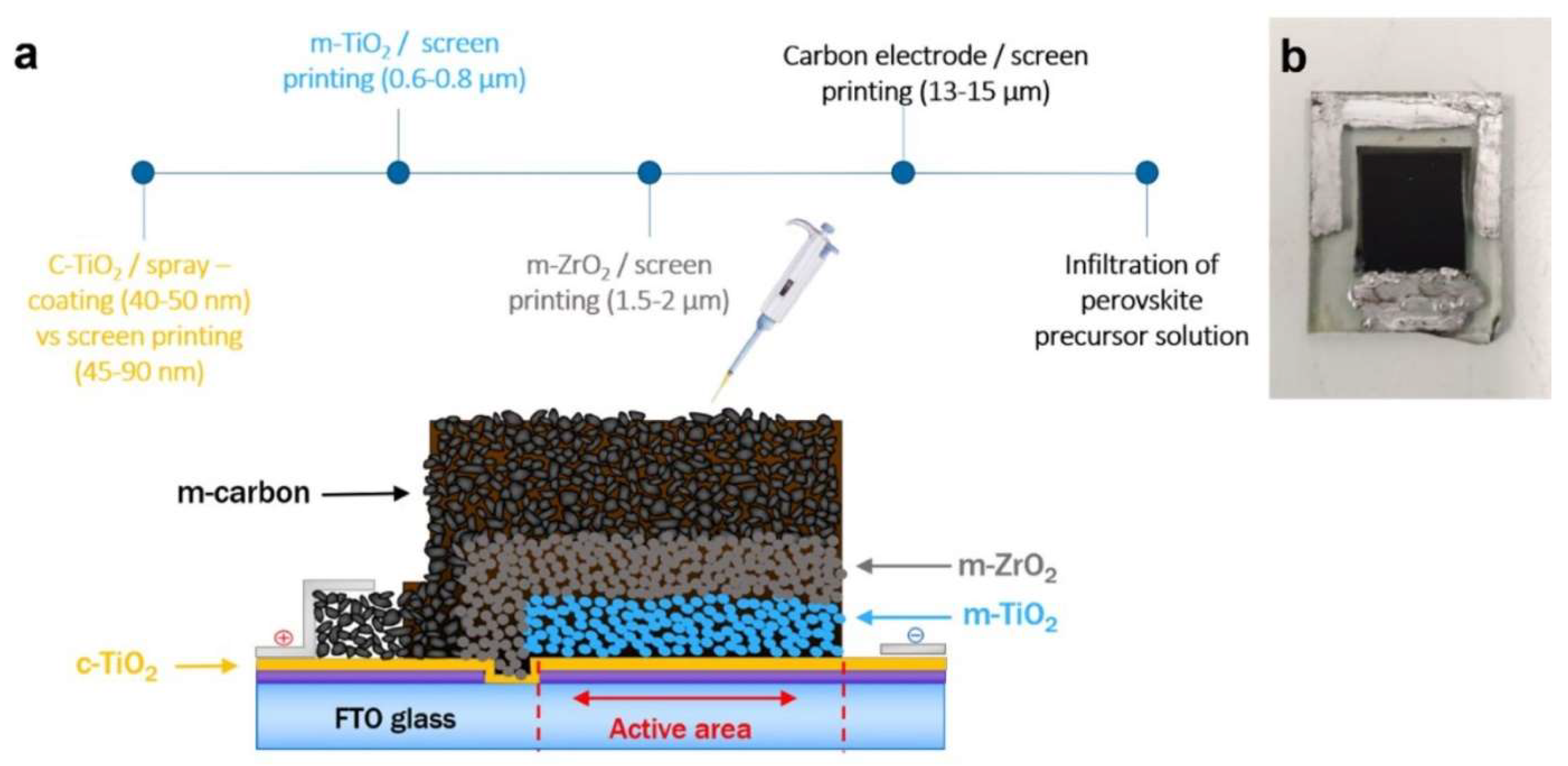
2.2. Fabrication of TiO2 Compact Layers

FTO substrates were cleaned with a solution of ~2% Hellmanex in deionised water, rinsed with acetone and IPA, and a 5 min plasma clean in O2. Samples with sprayed compact TiO2 layers were prepared by spray pyrolysis of 10% titanium diisopropoxide bis(acetylacetonate) in IPA at 300 °C. Two different screen-printed compact layers, in terms of thickness, were prepared as well. One printing of Ti-Nanoxide BL/SP commercial paste with a screen of 130-34 led to similar thickness to the sprayed one, while two printings with the same conditions led to higher thickness. After the printings, the samples were annealed at 550 °C.
For the TiCl4 treatment, samples were dipped into a 0.05 M TiCl4 solution in H2O for 30 min. Samples were then copiously rinsed and calcined at 500 °C.

2.3. Device Fabrication

For the device fabrication, FTO substrates were patterned with a Nb:YVO4 laser (532 nm) before the cleaning procedure. After the deposition of C-TiO2 (by spray pyrolysis or screen-printing together with the TiCl4 treatment), the mesoporous TiO2 paste was diluted 1:1 by weight in terpineol, screen-printed, and sintered at 550 °C. Next, the mesoporous ZrO2 and carbon were sequentially screen-printed, and each annealed at 400 °C. A perovskite precursor solution (0.439 g PbI2, 0.1514 g MAI and 0.0067 g 5-AVAI in 1 mL γ-Butyrolactone) was then drop cast (15 μL) onto the cooled stack. Devices were left in air for 10 min to allow the solution to percolate through the stack, before annealing in an oven for 1 h at 50 °C (Figure 1). The finished cells were then exposed to a standard 70% relative humidity process at 40 °C for 24 h to induce a recrystallisation [48] and then dried under vacuum before measuring.

2.4. Characterization Techniques

Optical transmission spectra of the tested TiO2 compact layers was examined using a Perkin Elmer UV/vis/NIR spectrophotometer Lambda 750 with a 100 mm InGaAs integrating sphere. Scans from 800 to 300 nm were taken with a 10 nm data interval at 266.75 nm min−1 with transmission mode.
The morphology of the tested films was examined using a HITACHI scanning electron microscope (SEM), while films thicknesses (Figure 1) were measured with a DEKTAK 150 profilometer system.
Cyclic voltammetry (CV) was conducted using a Zahner ZENNIUM X electrochemical workstation. Samples were mounted against an O-ring to define the area exposed to the electrolyte (~1 cm2). Measurements were performed at a scan rate of 50 mV s−1 in an electrolyte containing 0.5 mM potassium ferricyanide/ferrocyanide in aqueous 0.5 M KCl against a Ag/AgCl (3M KCl) reference electrode
IV testing of the cells was performed under a class AAA solar simulator (Newport Oriel Sol3A) at AM1.5 and 100 mW cm−2 illumination, calibrated using a KG5 filtered reference cell. The cell area was masked to 0.49 cm2 and devices were light soaked for 3 min before current density (J)–voltage (V) sweeps were performed from open-circuit voltage (VOC) to short-circuit current density (JSC) and vice-versa, at a rate of 330 mV/s using a Keithley 2400 source meter. For stabilised power output measurements, device bias was set to the maximum power point voltage as determined by the J–V sweep and current monitored under 100 mW cm−2 illumination for 200 s.

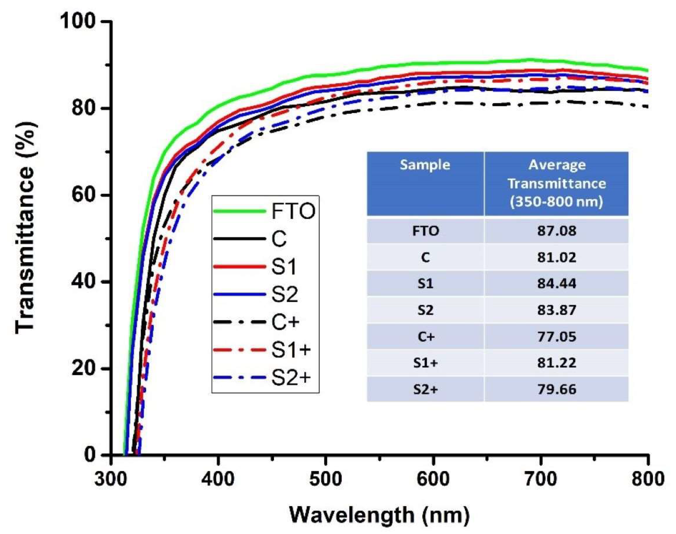
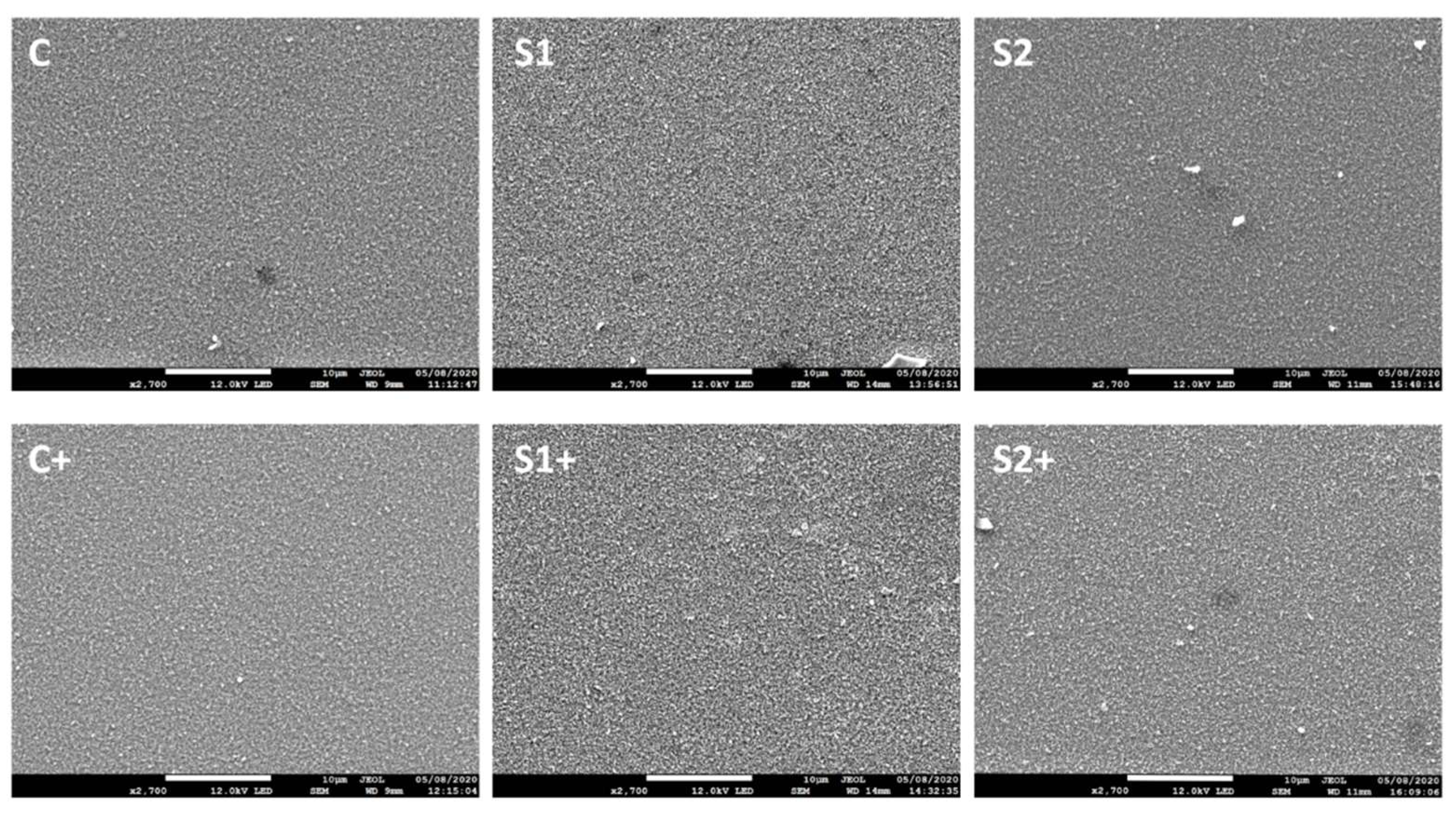
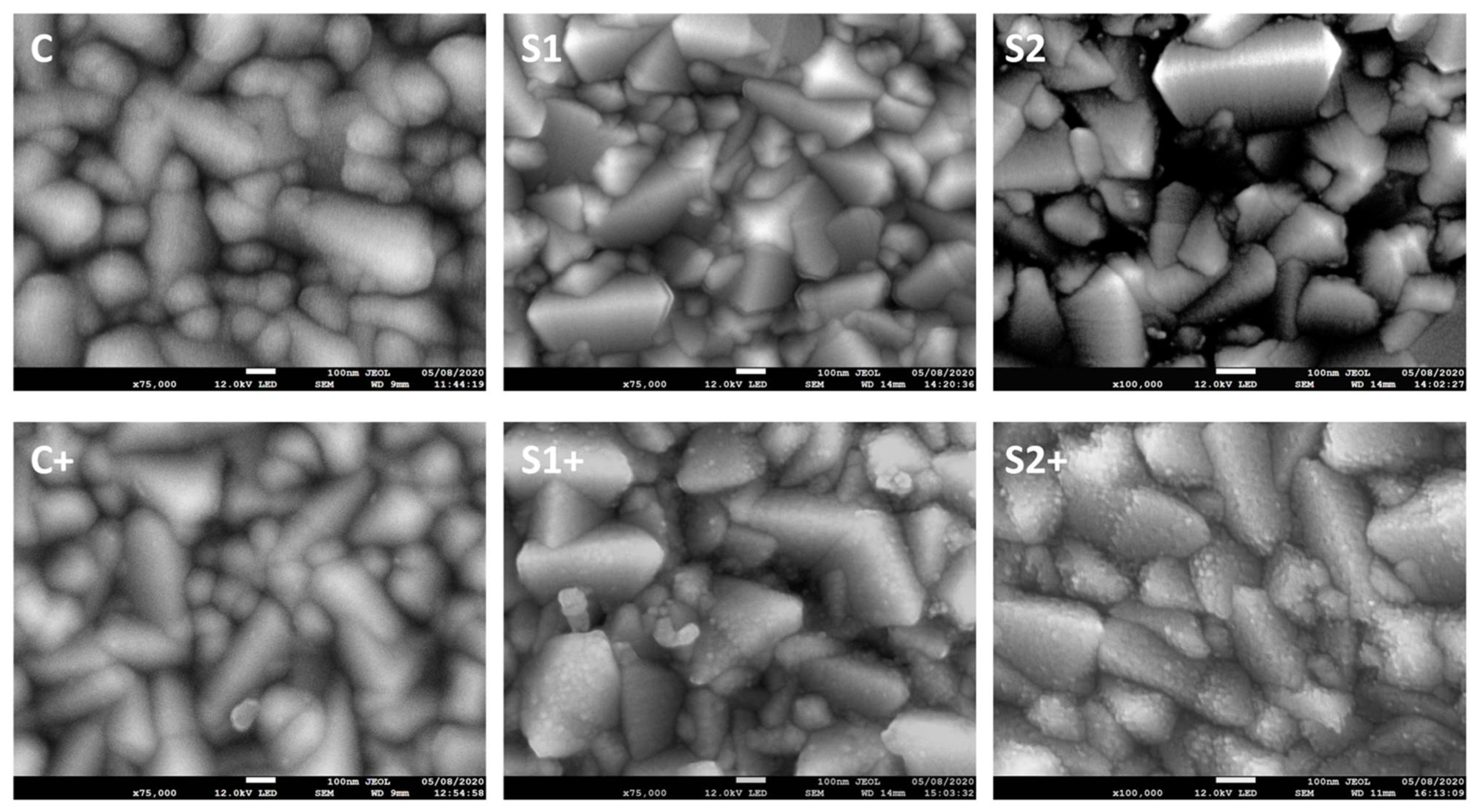
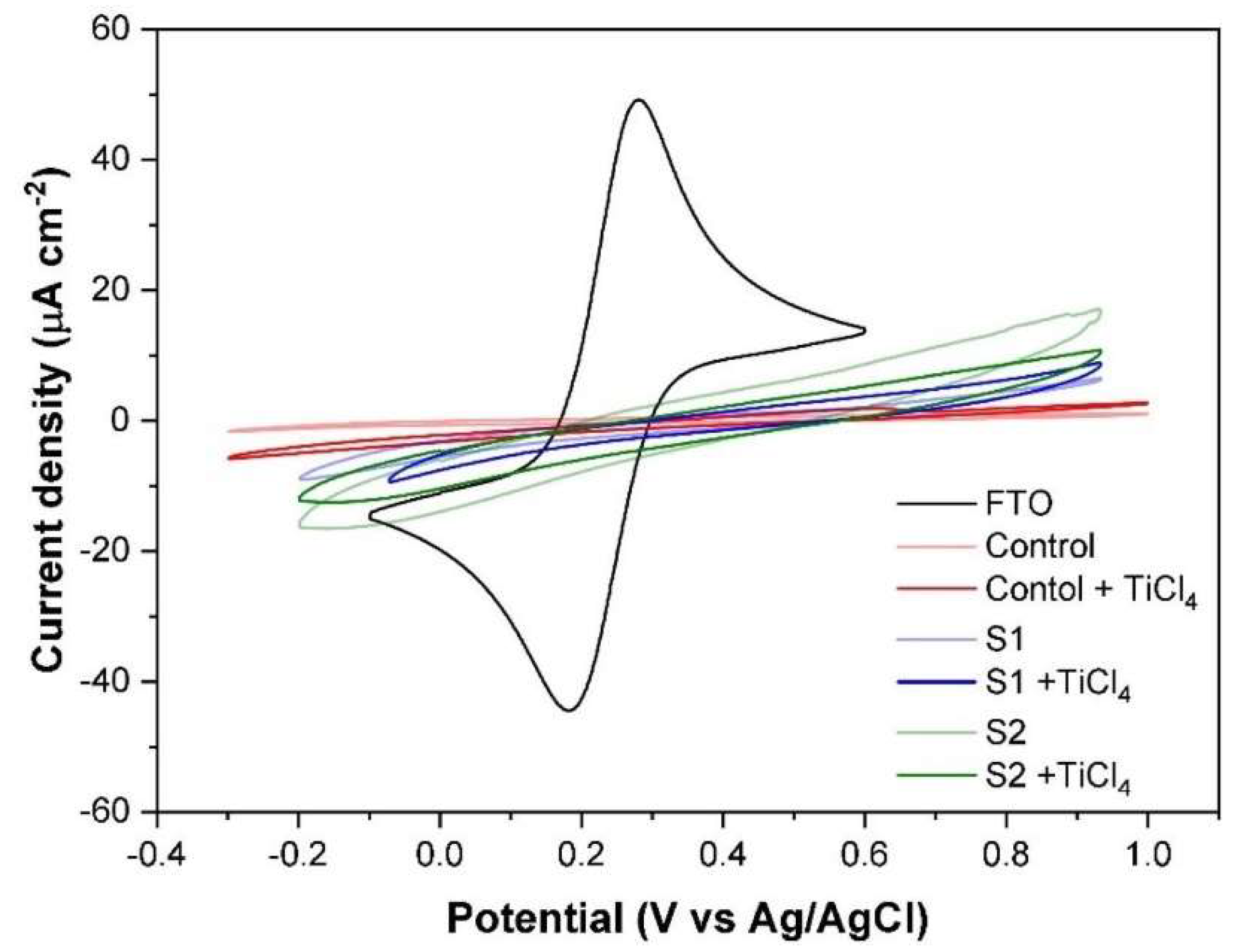
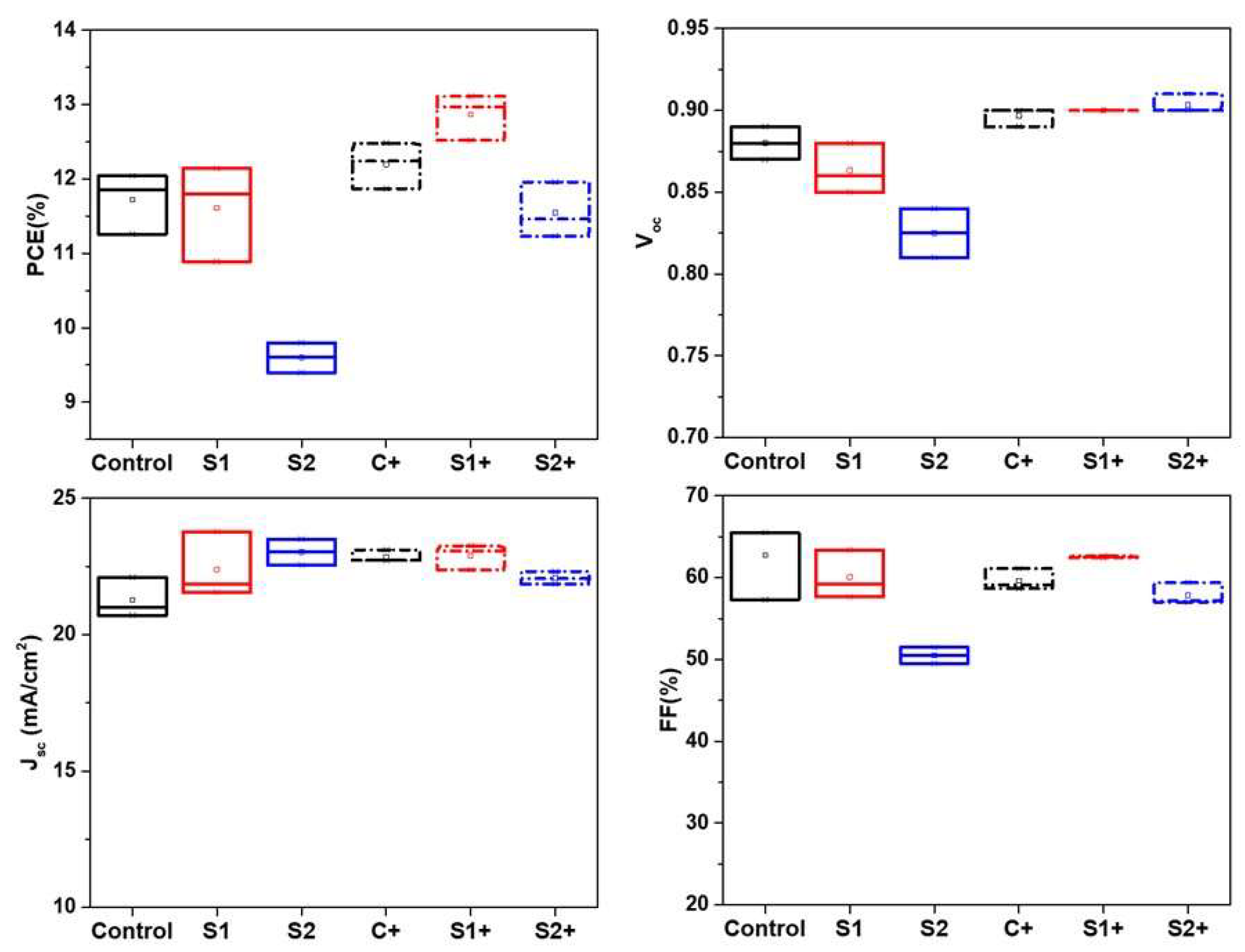
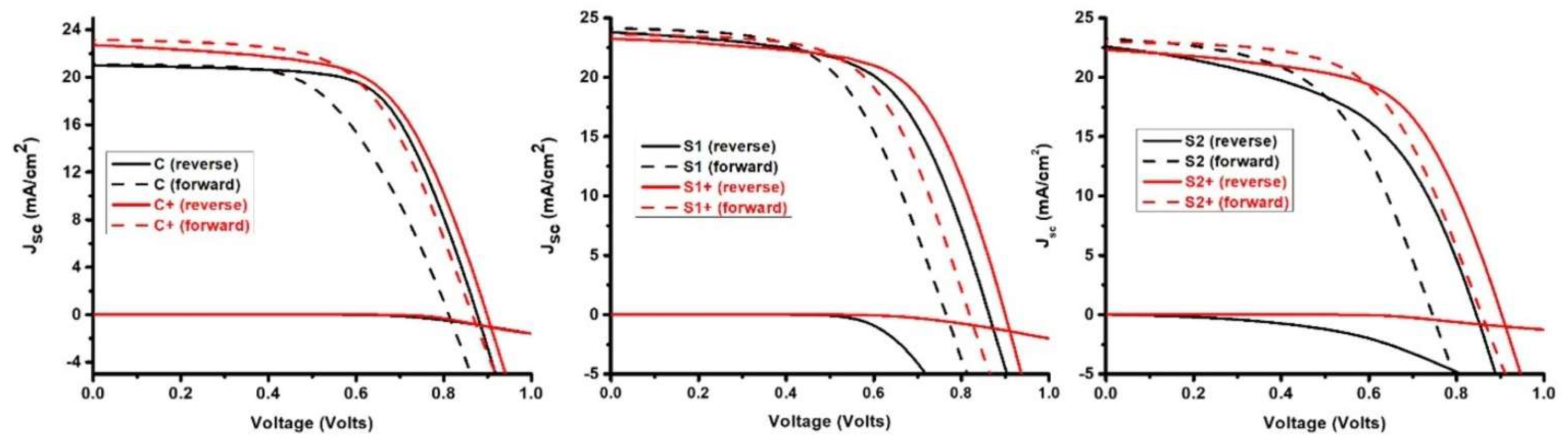
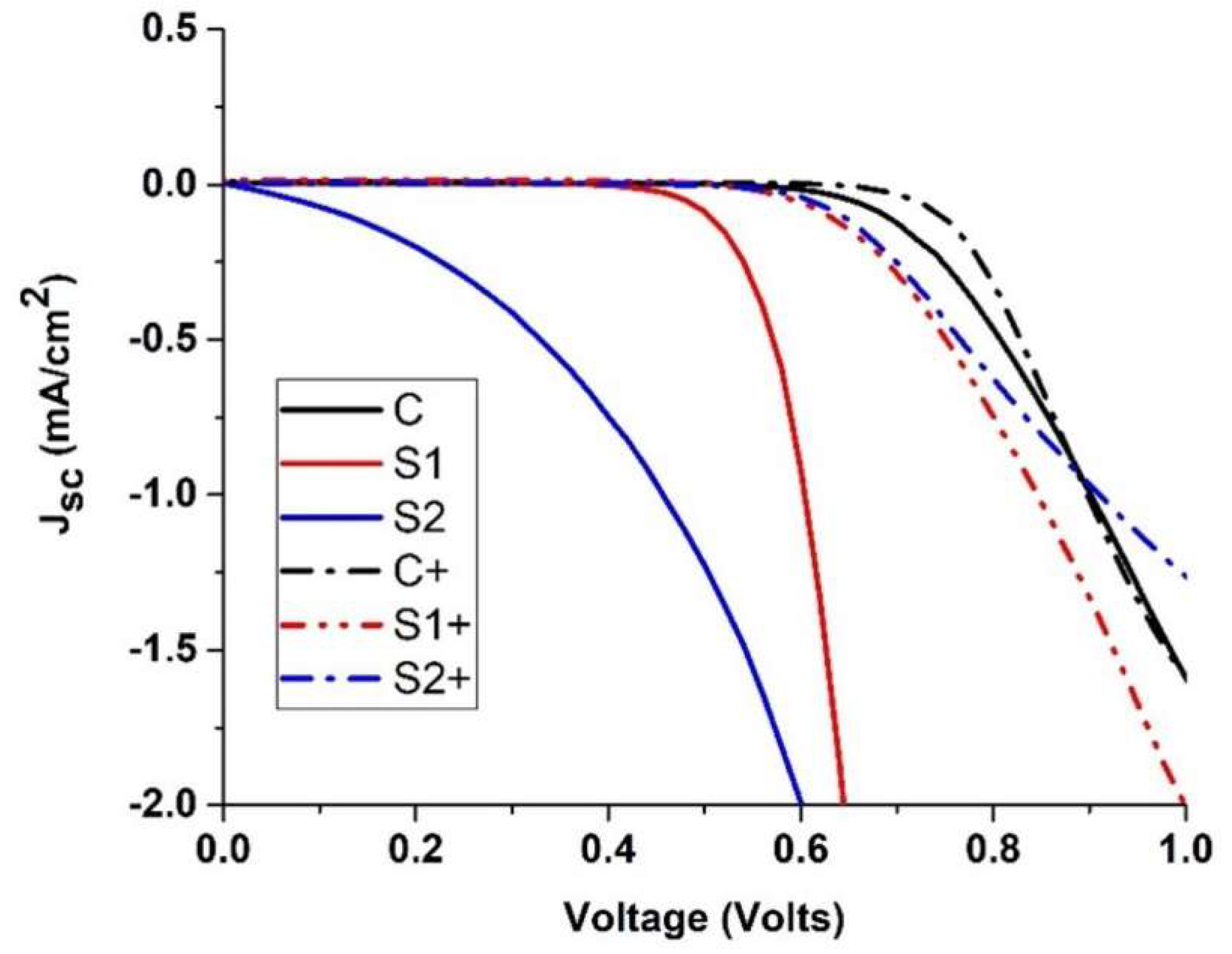
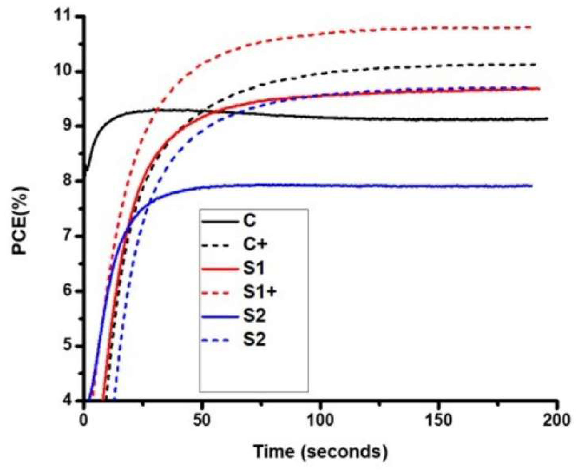
3. Results and Discussion

To investigate the viability of screen-printing for the C-TiO2 deposition, two different thicknesses were screen-printed on FTO substrates and compared to those deposited with the standard spray pyrolysis method. Τhe sprayed control samples (C) were found to be 40–50 nm. For the screen printed, a single print (S1) formed a 45–60 nm film, while two prints (S2) (without drying between printing) formed a 70–90 nm layer. Samples of each type were also exposed to a TiCl4 treatment, to produce C+, S1+, and S2+ (Table 1).
During PSC operation, light accesses the device via the glass/FTO substrate. Therefore, the most efficient compact layers will exhibit high transmission. Figure 2 shows optical transmission spectra for all tested compact layers, as well as plain FTO glass. Although coated samples exhibit lower transmission to plain FTO glass, they still exhibit high average optical transmissions of between 77% and 84% across the visible spectrum. Printed layers record higher transmission than sprayed, while the TiCl4 treatment reduces the value by around 4% for each case.
Surface SEM was performed to examine the C-TiO2 surface coverage and check for pinholes. As shown in in Figure 3, the sprayed sample and S1 printed sample look very similar, with both showing good FTO coverage. However, in the case of S2, there are some visible white spots, which likely correspond to pinholes. These pinholes can be attributed to the excessive thickness of the S2 sample: previous reports have proved that the cracking of TiO2 layers increases with the thickness of the layer, especially at FTO crystal boundaries, due to higher tension forces exerted on films in these areas [36,49]. Such pinholes could act as charge recombination centres and compromise Voc and the fill factor (FF) of the corresponding S2 C-PSCs.
Surface SEM images with higher resolution are shown in Figure 4, where we can more clearly observe individual C-TiO2 crystals and see the impact of TiCl4 treatment. The printed samples are very conformal, with more angular crystals compared to the sprayed one. In addition, the impact of the TiCl4 treatment is significantly evident on the printed samples (especially on the S2), whereas not so evident on the surface of the sprayed sample. This fact suggests that the angular crystals of the printed layers are potentially a more suitable surface for the binding of TiCl4.
Cyclic voltammetry is an electrochemical technique that can provide useful information for the quality of a compact layer on an FTO surface [50]. Figure 5 shows cyclic voltammograms of different C-TiO2 films and plain FTO exposed to potassium ferricyanide/ferrocyanide electrolyte. In this experiment, the ferricyanide/ferrocyanide solution acts as a model redox system in a three-electrode cell, while the tested sample acts as a working electrode. The molecules of the potassium ferricyanide/ferrocyanide redox couple are small enough to penetrate small pinholes and cracks in the C-TiO2 to reach the underlying FTO. The C-TiO2 surface coverage can therefore be estimated using the magnitude of the anodic current density in the cyclic voltammogram, as the C-TiO2 should form a dielectric contact with the redox couple and so repress the anodic current. Therefore, any anodic current will be a consequence of exposed FTO.
As there is minimal current, all the C-TiO2 samples present blocking ability over the voltage range compared to bare FTO. TiCl4 treatment decreases the anodic current in all the samples but has a higher effect in the case of the S2 printed layer, which seems to be of worse quality compared to S1 and sprayed layers. This result confirms our observations from the surface SEM images where the presence of some pinholes on S2 surface were evident and the TiCl4 treatment had higher impact on it.
C-PSCs fabricated with the different C-TiO2 layers and the statistical results of their performance are shown in Figure 6 and Table 2. S1 devices recorded average PCEs of 11.61 ± 0.37%, which is comparable with the average PCEs of the sprayed C-TiO2 devices (11.72 ± 0.24%). Printed devices exhibited higher currents compared to the cells with sprayed C-TiO2, which could be due to the slightly higher transmittance. Higher transmittance results in higher light absorption into the perovskite layer and, therefore, higher current. In contrast, devices with thicker S2 layers recorded lower average efficiency (9.60 ± 0.20%) due to lower values of Voc and FF, likely a consequence of the pinholes observed in Figure 3. TiCl4 treatment was beneficial for all devices, particularly impacting those with printed compact layers. More specifically, TiCl4 treatment increased the average PCE from 11.61 ± 0.24% for S1 to 12.87 ± 0.18% for S1+, while TiCl4 in thicker S2 layers increased the average efficiency from 9.60 ± 0.2% to 11.55 ± 0.22%. In the case of the sprayed compact layer, the improvement is less marked (from 11.72 ± 0.24% to 12.2 ± 0.18%).
These results correlate well with the CV measurements, where TiCl4 had the greatest impact on the thick, lower quality S2 samples. The higher impact of TiCl4 can also be explained by the surface SEM images in Figure 4, where TiCl4 is more evident on the angular crystals.
The current density (J)–voltage (V) of the best performing C-PSCs, are shown in Figure 7, with detailed photovoltaic parameters presented in Table 3. A champion PCE of 13.11% was recorded for an S1+ device, while the untreated S1 champion exhibited a PCE of 12.14%. In the case of S2 samples the PCE of the champion device was lower (9.8%). However, the use of TiCl4 increased the efficiency to 11.96%. The device with the sprayed compact layer, recorded a champion PCE at 11.86%, which increased with the TiCl4 treatment (12.48%). The higher Jsc in the case of printed C-TiO2 can be attributed to the higher transmittance of these layers, while the higher Voc and FF of the sprayed sample can be attributed to the lower incidence of pinholes.
Dark current measurements of the champion devices are shown in Figure 8. In these measurements, increased onset voltage values indicate a reduction in the electron–hole recombination between perovskite and the TiO2 and FTO conduction bands [38]. It is obvious that the devices with printed compact layers show increased recombination phenomena since the onset voltage value is low, especially in the case of the S2 device. This is reasonable if we consider observed pinholes, which act as charge recombination centres (Figure 3). However, this behaviour is not apparent after TiCl4 treatment, where the onset voltage is increased in all the samples, particularly S2. This confirms our previous conclusions from SEM and CV characterisations regarding the contribution of TiCl4 in improving the printed C-TiO2 quality compact layers.
To provide additional confidence in the device performance, stabilised current measurements were also performed on the devices and the corresponding graphs of the champion cells are shown in Figure 9.
These measurements confirm the observed trend from the J–V measurements, where devices with S1 and sprayed compact layers recorded similar PCEs, while thicker blocking layers (S2) led to lower efficiencies. As with other measurements, all devices with TiCl4 treated layers showed improved PCEs, with the highest improvement obtained in the case of the S2 device. Once again, the use of S1+ layer led to the highest efficiency (10.81%). The conversion efficiencies become stable between 50 and 100 s after the start of the measurement, and in all the samples, the recorded J-V PCE is higher than the stabilised PCE. This behaviour is frequently observed in C-PSCs and is attributed to imbalanced charge extraction, as electrons are generated close to TiO2 electron transporting layer while holes need to travel through a thick ZrO2 layer to access the carbon electrode [51,52]. It is also noteworthy that devices were light soaked for 3 min before current density (J)–voltage (V) sweeps were performed from open-circuit voltage (VOC) to short-circuit current density (JSC) and vice-versa. This light soaking is important for C-PSCs to achieve their highest performances as the presence of the AVA molecule inhibits the movement of ions [53].
All the above results confirm the criticality of C-TiO2 layer thickness, in accordance with previous publications [34,36,44,49]. Films with thickness from 40–60 nm (sprayed and S1) are pinhole-free (Figure 3), with high blocking ability (Figure 5). The comparable PCE results of the devices with the S1 and sprayed C-TiO2 layers show that screen-printing is a viable substitution for spray pyrolysis in depositing C-TiO2 films for highly efficient C-PSCs. The fact that S1 cells exhibit higher Jsc is also encouraging. Films with thicknesses of more than 70 nm present pinholes (Figure 3) due to higher tension forces exerted on the films, which result in C-TiO2 cracking of layers at FTO crystal edges. These pinholes act as charge recombination centres and, thus, the corresponding cells record lower Voc and FF, and as a result, lower PCE. It should also be noted that TiCl4 treatments proved more beneficial in the case of printed compact layers. The more angular crystals in these printed layers (Figure 4) may provide cleaner, more easily accessible binding sites for the TiCl4 reducing the impact of random printing flaws and improving the layer quality.

4. Conclusions

In this work, we study the surface morphology and the optical and electrochemical properties of screen-printed TiO2 compact layers, in order to investigate their viability for application in C-PSCs. A high quality, pinhole-free, screen-printed compact layer with over 84% transmittance and similar thickness to the standard sprayed blocking layer was obtained. C-PSCs fabricated with such printed layers exhibited 11.86% average PCE, comparable to that of devices produced via spray pyrolysis. Furthermore, TiCl4 treatment was found to drastically improve the quality of the screen-printed films, with the corresponding devices producing a champion PCE of 13.11%.
In summary, the screen-printing was found to be a suitable method for depositing C-TiO2 in C-PSCs. Additionally, layer quality and device performance may be significantly enhanced by employing a TiCl4 treatment. As screen-printing is cheap and easy to scale up, these results could enhance the production of highly efficient solar cells and modules, hence facilitating the production of commercially competitive C–PSCs.

Author Contributions

Conceptualization, D.R. and T.W.; methodology, D.R. and S.M.P.M.; software, D.R., C.A.W. and A.P.; validation, D.R. and S.M.P.M.; formal analysis, D.R., C.A.W. and A.P.; investigation, D.R.; writing—original draft preparation, D.R.; writing—review and editing, T.W. and C.A.W.; supervision, T.W. and M.C.; project administration, T.W.; funding acquisition, T.W. All authors have read and agreed to the published version of the manuscript.

Funding

This work was made possible by support from the UKRI Global Challenge Research Fund project SUNRISE (EP/P032591/1) and through the funding from the SPECIFIC Innovation and Knowledge Centre by the Engineering and Physical Science Research Council (EP/N020863/1), Innovate UK (920036), Newton fund, Royal Society, the European Regional Development Fund (c80892) through the Welsh Government, a Royal Society International Collaboration award (ICA\R1\191321), and the Newton Fund Impact Scheme (541128962). This work was also funded by the PV-Interfaces (EP/R032750/1), ATIP (EP/T028513/1), and the European Regional Development Fund (ERDF): SPARC II.

Institutional Review Board Statement

Not applicable.

Informed Consent Statement

Not applicable.

Data Availability Statement

Not applicable.

Conflicts of Interest

The authors declare no conflict of interest.

References

  1. Kojima, A.; Teshima, K.; Shirai, Y.; Miyasaka, Y. Organometal halide perovskites as visible-light sensitizers for photovoltaic cells. J. Am. Chem. Soc. 2009, 131, 6050–6051. [Google Scholar] [CrossRef] [PubMed]
  2. Lee, M.M.; Teuscher, J.; Miyasaka, T.; Murakami, T.N.; Snaith, H.J. Efficient hybrid solar cells based on meso-superstructured organometal halide perovskites. Science 2012, 338, 643–647. [Google Scholar] [CrossRef] [PubMed] [Green Version]
  3. Yang, W.S.; Noh, J.H.; Jeon, N.J.; Kim, Y.C.; Ryu, S.; Seo, J.; Seok, S.I. High-performance photovoltaic perovskite layers fabricated through intramolecular exchange. Science 2015, 348, 1234–1237. [Google Scholar] [CrossRef] [PubMed]
  4. Zhao, D.; Yu, Y.; Wang, C.; Liao, W.; Shrestha, N.; Grice, C.R.; Climaroli, A.J.; Guan, L.; Ellingson, R.J.; Zhu, K.; et al. Low-bandgap mixed tin–lead iodide perovskite absorbers with long carrier lifetimes for all-perovskite tandem solar cells. Nat. Energy 2017, 2, 17018. [Google Scholar] [CrossRef]
  5. Yang, W.S.; Park, B.W.; Jung, E.H.; Jeon, N.J.; Kim, Y.C.; Lee, D.U.; Shin, S.S.; Seo, J.; Kim, E.K.; Noh, J.H.; et al. Iodide management in formamidinium-lead-halidebased perovskite layers for efficient solar cells. Science 2017, 356, 1376–1379. [Google Scholar] [CrossRef] [Green Version]
  6. Best Research-Cell Efficiency Chart, Photovoltaic Research, NREL. Available online: https://www.nrel.gov/pv/cell-efficiency.html (accessed on 24 January 2021).
  7. Snaith, H.J. Present status and future prospects of perovskite photovoltaics. Nat. Mater. 2018, 17, 372–376. [Google Scholar] [CrossRef]
  8. Zhang, M.; Lyu, M.; Yu, H.; Yun, J.; Wang, Q.; Wang, L. Stable and low-cost mesoscopic CH3NH3PbI2Br perovskite solar cells by using a thin poly(3-hexylthiophene) layer as a hole transporter. Chem. Eur. J. 2015, 21, 434–439. [Google Scholar] [CrossRef]
  9. Baker, J.A.; Mouhamad, Y.; Hooper, K.; Burkitt, D.; Geoghegan, M.; Watson, T.M. From spin coating to roll-to-roll: Investigating the challenge of upscaling lead halide perovskite solar cells. IET Renew. Power Gener. 2017, 11, 546–549. [Google Scholar] [CrossRef] [Green Version]
  10. Ku, Z.; Rong, Y.; Xu, M.; Liu, T.; Han, H. Full Printable Processed Mesoscopic CH3NH3PbI3/TiO2 Heterojunction Solar Cells with Carbon Counter Electrode. Sci. Rep. 2013, 3, 3132. [Google Scholar] [CrossRef] [Green Version]
  11. Meroni, S.M.P.; Mouhamad, Y.; De Rossi, F.; Pockett, A.; Baker, J.; Escalante, R.; Searle, J.; Carnie, M.J.; Jewell, E.; Oskam, G.; et al. Homogeneous and highly controlled deposition of low viscosity inks and application on fully printable perovskite solar cells. Sci. Technol. Adv. Mater. 2018, 19, 1–9. [Google Scholar] [CrossRef] [Green Version]
  12. Mei, A.; Li, X.; Liu, L.; Ku, Z.; Liu, T.; Rong, Y.; Xu, M.; Hu, M.; Chen, J.; Yang, Y.; et al. A hole-conductor-free, fully printable mesoscopic perovskite solar cell with high stability. Science 2014, 345, 295–298. [Google Scholar] [CrossRef] [PubMed]
  13. Grancini, G.; Carmona, C.R.; Zimmermann, I.; Mosconi, E.; Lee, X.; Martineau, D.; Narbey, S.; Oswald, F.; De Angelis, F.; Graetzel, M.; et al. One-Year stable perovskite solar cells by 2D/3D interface engineering. Nat. Commun. 2017, 8, 15684. [Google Scholar] [CrossRef] [PubMed]
  14. Mei, A.; Sheng, Y.; Ming, Y.; Hu, Y.; Rong, Y.; Zhang, W.; Luo, S.; Na, G.; Tian, C.; Hou, X.; et al. Stabilizing Perovskite Solar Cells to IEC61215:2016 Standards with over 9,000-h Operational Tracking. Joule 2020, 4, 2646–2660. [Google Scholar] [CrossRef]
  15. Chen, H.; Yang, S. Carbon-based perovskite solar cells without hole transport materials: The front runner to the market? Adv. Mater. 2017, 29, 1603994. [Google Scholar] [CrossRef]
  16. Meroni, S.M.P.; Worsley, C.; Raptis, D.; Watson, T.M. Triple-Mesoscopic Carbon Perovskite Solar Cells: Materials, Processing and Applications. Energies 2021, 14, 386. [Google Scholar] [CrossRef]
  17. Tao, R.; Fang, W.; Li, F.; Sun, Z.; Xu, L. Lanthanide-containing polyoxometalate as luminescent down-conversion material for improved printable perovskite solar cells. J. Alloys Compd. 2020, 823, 153738. [Google Scholar] [CrossRef]
  18. Liu, T.; Xiong, Y.; Mei, A.; Hu, Y.; Rong, Y.; Xu, M.; Wang, Z.; Lou, L.; Du, D.; Zheng, S.; et al. Spacer layer design for efficient fully printable mesoscopic perovskite solar cells. RSC Adv. 2019, 9, 29840–29846. [Google Scholar] [CrossRef] [Green Version]
  19. Mathiazhagan, G.; Wagner, L.; Bogati, S.; Ünal, K.Y.; Bogachuk, D.; Kroyer, T.; Mastroianni, S.; Hinsch, A. Double-Mesoscopic Hole-Transport-Material-Free Perovskite Solar Cells: Overcoming Charge-Transport Limitation by Sputtered Ultrathin Al2O3 Isolating Layer. ACS Appl. Nano Mater. 2020, 3, 2463–2471G. [Google Scholar] [CrossRef]
  20. Raptis, D.; Stoichkov, V.; Meroni, S.M.; Pockett, A.; Worsley, C.A.; Carnie, M.; Worsley, D.A.; Watson, T.M. Enhancing fully printable mesoscopic perovskite solar cell performance using integrated metallic grids to improve carbon electrode conductivity. Curr. Appl. Phys. 2020, 20, 619–627. [Google Scholar] [CrossRef]
  21. Tian, C.; Mei, A.; Zhang, S.; Tian, H.; Liu, S.; Qin, F.; Xiong, Y.; Rong, Y.; Hu, Y.; Zhou, Y.; et al. Oxygen management in carbon electrode for high-performance printable perovskite solar cells. Nano Energy 2018, 53, 160–167. [Google Scholar] [CrossRef]
  22. Zhang, H.; Wang, H.; Williams, S.T.; Xiong, D.; Zhang, W.; Chueh, C.C.; Chen, W.; Jen, A.K.Y. SrCl2 derived perovskite facilitating a high efficiency of 16% in holeconductor-free fully printable mesoscopic perovskite solar cells. Adv. Mater. 2017, 29, 1606608. [Google Scholar] [CrossRef] [PubMed]
  23. Chen, X.; Xia, Y.; Huang, Q.; Li, Z.; Mei, A.; Hu, A.; Wang, T.; Cheacharoen, R.; Rong, Y.; Han, H. Tailoring the Dimensionality of Hybrid Perovskites in Mesoporous Carbon Electrodes for Type-II Band Alignment and Enhanced Performance of Printable Hole-Conductor-Free Perovskite Solar Cells. Adv. Energy Mater. 2021, 11, 2100292. [Google Scholar] [CrossRef]
  24. Liu, S.; Zhang, D.; Shenga, Y.; Zhang, W.; Qin, Z.; Qin, M.; Li, S.; Wang, Y.; Gao, C.; Wang, Q.; et al. Highly oriented MAPbI3 crystals for efficient hole-conductor-free printable mesoscopic perovskite solar cells. Fundam. Res. 2021, 2, 276–283. [Google Scholar] [CrossRef]
  25. Priyadarshi, A.; Haur, L.J.; Murray, P.; Fu, D.; Kulkarni, S.; Xing, G.; Sum, T.C.; Mathews, N.; Mhaisalkar, S.G. A large area (70 cm2) monolithic perovskite solar module with a high efficiency and stability. Energy Environ. Sci. 2016, 9, 3687–3692. [Google Scholar] [CrossRef]
  26. Hu, Y.; Si, S.; Mei, A.; Rong, Y.; Liu, H.; Li, X.; Han, H. Stable Large-Area (10 × 10 cm2) Printable Mesoscopic Perovskite Module Exceeding 10% Efficiency. Sol. RRL 2017, 1, 1600019. [Google Scholar] [CrossRef]
  27. De Rossi, F.; Baker, J.; Beynon, D.; Hooper, K.E.A.; Meroni, S.M.P.; Williams, D.; Wei, Z.; Yasin, A.; Charbonneau, C.; Jewell, E.H.; et al. All Printable Perovskite Solar Modules with 198 cm2 Active Area and Over 6% Efficiency. Adv. Mater. Technol. 2018, 3, 1800156. [Google Scholar] [CrossRef] [Green Version]
  28. Worsley, C.; Raptis, D.; Meroni, S.; Patidar, R.; Pockett, A.; Dunlop, T.; Potts, S.; Bolton, R.; Charbonneau, C.; Carnie, M.; et al. Green solvent engineering for enhanced performance and reproducibility in printed carbon-based mesoscopic perovskite solar cells and modules. Mater. Adv. 2022, 3, 1125–1138. [Google Scholar] [CrossRef]
  29. Liu, D.; Kelly, T.L. Perovskite solar cells with a planar heterojunction structure prepared using room-temperature solution processing techniques. Nat. Photonics 2013, 8, 133–138. [Google Scholar] [CrossRef]
  30. Burschka, J.; Pellet, N.; Moon, S.J.; Baker, R.H.; Gao, P.; Nazeeruddin, M.K.; Gratzel, M. Sequential deposition as a route to high-performance perovskite-sensitized solar cells. Nature 2013, 499, 316–319. [Google Scholar] [CrossRef]
  31. Liu, M.Z.; Johnston, M.B.; Snaith, H.J. Efficient planar heterojunction perovskite solar cells by vapour deposition. Nature 2013, 501, 395–398. [Google Scholar] [CrossRef]
  32. Liu, J.; Wang, G.; Luo, K.; He, X.; Ye, Q.; Liao, C.; Mei, J. Understanding the role of the electron-transport layer in highly efficient planar perovskite solar cells. Chem. Phys. Chem. 2017, 18, 617–625. [Google Scholar] [CrossRef] [PubMed]
  33. Zhang, S.; Lei, L.; Yang, S.; Li, X.; Liu, Y.; Gao, Q.; Gao, X.; Cao, Q.; Yu, Y. Influence of TiO2 blocking layer morphology on planar heterojunction perovskite solar cells. Chem. Lett. 2016, 45, 592–594. [Google Scholar] [CrossRef]
  34. Mohamad Noh, M.F.; Teh, C.H.; Daik, R.; Lim, E.L.; Yap, C.C.; Ibrahim, M.A.; Ludin, N.A.; Mohd Yusoff, A.R.; Jang, J.; Mat Teridi, M.A. The architecture of the electron transport layer for a perovskite solar cell. J. Mater. Chem. C 2018, 6, 682–712. [Google Scholar] [CrossRef]
  35. Rong, Y.; Huawei, L.; Ravishankar, S.; Liu, H.; Hou, X.; Sheng, Y.; Mei, A.; Wang, Q.; Li, D.; Xu, M.; et al. Tunable hysteresis effect for perovskite solar cells. Energy Environ. Sci. 2017, 10, 2383–2391. [Google Scholar] [CrossRef]
  36. Lewis, A.; Troughton, J.R.; Smith, B.; McGettrick, J.; Dunlop, T.; De Rossi, F.; Pockett, A.; Spence, M.; Carnie, M.J.; Watson, T.M.; et al. In-depth analysis of defects in TiO2 compact electron transport layers and impact on performance and hysteresis of planar perovskite devices at low light. Sol. Energy Mater. Sol. Cells 2020, 209, 110448. [Google Scholar] [CrossRef]
  37. Smith, B.; Troughton, J.; Lewis, A.; McGettrick, J.; Pockett, A.; Carnie, M.; Charbonneau, C.; Pleydell-Pearce, C.; Searle, J.; Warren, P.; et al. Mass Manufactured Glass Substrates Incorporating Prefabricated Electron Transport Layers for Perovskite Solar Cells. Adv. Mater. Interfaces 2019, 6, 1801773. [Google Scholar] [CrossRef]
  38. Hu, H.; Dong, B.; Hu, H.; Chen, F.; Kong, M.; Zhang, Q.; Luo, T.; Zhao, L.; Guo, Z.; Li, J.; et al. Atomic Layer Deposition of TiO2 for a High-Efficiency Hole-Blocking Layer in Hole-Conductor-Free Perovskite Solar Cells Processed in Ambient Air. ACS Appl. Mater. Interfaces 2016, 8, 17999–18007. [Google Scholar] [CrossRef]
  39. Zhang, C.; Luo, Y.; Chen, X.; Ou-Yang, W.; Chen, Y.; Sun, Z.; Huang, S. Influence of different TiO2 blocking films on the photovoltaic performance of perovskite solar cells. Appl. Surf. Sci. 2016, 388, 82–88. [Google Scholar] [CrossRef]
  40. Du, Y.Y.; Cai, H.K.; Wu, Y.H.; Xing, Z.X.; Li, Z.L.; Xu, J.; Huang, L.; Ni, J.; Li, J.; Zhang, J.J. Enhanced planar perovskite solar cells with efficiency exceeding 16% via reducing the oxygen vacancy defect state in titanium oxide electrode. Phys. Chem. Chem. Phys. 2017, 19, 13679–13686. [Google Scholar] [CrossRef]
  41. Yella, A.; Heiniger, L.P.; Gao, P.; Nazeeruddin, M.K.; Gratzel, M. Nanocrystalline rutile electron extraction layer enables low-temperature solution processed perovskite photovoltaics with 13.7% efficiency. Nano Lett. 2014, 14, 2591–2596. [Google Scholar] [CrossRef]
  42. Zhou, P.; Wu, J.H.; Tu, Y.G.; Zhen, M.; Huo, J.H.; Wei, Y.L.; Lan, Z. Tin oxide nanosheets as efficient electron transporting materials for perovskite solar cells. Sol. Energy 2016, 137, 579–584. [Google Scholar] [CrossRef]
  43. Wang, E.; Chen, P.; Yin, X.; Gao, B.; Que, W. Boosting efficiency of planar heterojunction perovskite solar cells by a low temperature TiCl4 treatment. J. Adv. Dielectr. 2018, 8, 18500091. [Google Scholar] [CrossRef] [Green Version]
  44. Kim, B.; Il So, C.; Guk Ko, S.; Ri, J.H.; Il Ryu, G.; Su Sonu, G. Effects of TiCl4 post-treatment on the performance of hole transport material-free, screen printable mesoscopic perovskite solar cells with carbon electrode. Thin Solid Films 2019, 692, 137627. [Google Scholar] [CrossRef]
  45. Hvojnika, M.; Popovičová, A.M.; Pavličková, M.; Hatala, M.; Gemeiner, P.; Müllerová, J.; Tomanová, K.; Mikula, M. Solution-processed TiO2 blocking layers in printed carbon-based perovskite solar cells. Appl. Surf. Sci. 2021, 536, 147888. [Google Scholar] [CrossRef]
  46. Bashir, A.; Shukla, S.; Lew, J.H.; Shukla, S.; Bruno, A.; Gupta, D.; Baikie, T.; Patidar, R.; Akhter, Z.; Priyadarshi, A.; et al. Spinel Co3O4 nanomaterials for efficient and stable large area carbon-based printed perovskite solar cells. Nanoscale 2018, 10, 2341–2350. [Google Scholar] [CrossRef] [PubMed]
  47. Keremane, K.S.; Prathapani, S.; Jia Haur, L.; Bahulayan, D.; Adhikari, A.V.; Priyadarshi, A.; Subodh, A.; Mhaisalkar, G. Solvent selection for highly reproducible carbon-based mixed-cation hybrid lead halide perovskite solar cells via adduct approach. Sol. Energy 2020, 199, 761–771. [Google Scholar] [CrossRef]
  48. Troughton, J.; Hooper, K.; Watson, T.M. Humidity resistant fabrication of CH3NH3PbI3 perovskite solar cells and modules. Nano Energy 2017, 39, 60–68. [Google Scholar] [CrossRef] [Green Version]
  49. Mahé, M.; Heintz, J.M.; Rödel, J.; Reynders, P. Cracking of titania nanocrystalline coatings. J. Eur. Ceram. Soc. 2008, 28, 2003–2010. [Google Scholar] [CrossRef] [Green Version]
  50. Kavan, L.; Tétreault, N.; Moehl, T.; Grätzel, M. Electrochemical characterization of TiO2 blocking layers for dye-sensitized solar cells. J. Phys. Chem. C 2014, 118, 16408–16418. [Google Scholar] [CrossRef]
  51. Zimmermann, I.; Gratia, P.; Martineau, D.; Grancini, G.; Audinot, J.N.; Wirtz, T.; Nazeeruddin, M.K. Improved efficiency and reduced hysteresis in ultra-stable fully printable mesoscopic perovskite solar cells through incorporation of CuSCN into the perovskite layer. J. Mater. Chem. A 2019, 7, 8073–8077. [Google Scholar] [CrossRef]
  52. Worsley, C.; Raptis, D.; Meroni, M.; Doolin, A.; Rodriguez, R.; Davies, M.; Watson, T. γ-Valerolactone: A Nontoxic Green Solvent for Highly Stable Printed Mesoporous Perovskite Solar Cells. Energy Technol. 2021, 9, 2100312. [Google Scholar] [CrossRef]
  53. Pockett, A.; Raptis, D.; Meroni, S.; Baker, J.; Watson, T.; Carnie, M. Origin of Exceptionally Slow Light Soaking Effect in Mesoporous Carbon Perovskite Solar Cells with AVA Additive. J. Phys. Chem. C 2019, 18, 11414–11421. [Google Scholar] [CrossRef] [Green Version]
Figure 1. (a) Schematic representation and fabrication method of standard C-PSC. (b) Image of a 1 cm2 active area C-PSC.
Solar 02 00016 g001
Figure 2. Optical transmission spectra for the tested compact layers and plain FTO glass. The embedded table shows the average transmission (AT) of the samples across the visible spectrum.
Solar 02 00016 g002
Figure 3. Surface SEM images of the tested C-TiO2 layers that showing comparative coverage of the FTO glass. Scale bar is 10 µm.
Solar 02 00016 g003
Figure 4. Higher resolution surface SEM images that show the impact of TiCl4 treatment in the tested films. Scale bar is 100 nm.
Solar 02 00016 g004
Figure 5. CV measurements of all the tested layers and FTO glass.
Solar 02 00016 g005
Figure 6. Statistical results of C-PSCs with different compact layers of TiO2. Black represents the control, red represents those with a single printed layer and blue represents those with a double printed layer.
Solar 02 00016 g006
Figure 7. JV curves of the champion devices with the different C-TiO2 blocking layers.
Solar 02 00016 g007
Figure 8. JV curves of the champion devices with the different blocking layers in the dark.
Solar 02 00016 g008
Figure 9. Stabilised PCEs at one sun of devices with different TiO2 blocking layers.
Solar 02 00016 g009
Table 1. Nomenclature of the different C-TiO2 samples.
Type of C-TiO2 SamplesNomenclature
Sprayed control samplesC
Single printing samplesS1
Two printing samplesS2
Control samples (sprayed) + TiCl4 treatmentC+
Single printing samples + TiCl4 treatmentS1+
Two printing samples + TiCl4 treatmentS2
Table 2. Average values of photovoltaic parameters of C-PSCs with different TiO2 compact layers.
DevicePCE (%)Jsc (mA/cm2)Voc (Volts)FF (%)
C11.72 ± 0.2421.27 ± 0.420.88 ±0.0162.78 ± 2.71
S111.61 ± 0.3722.39 ± 0.700.86 ± 0.0160.08 ± 1.71
S29.60 ± 0.2023.03 ± 0.480.83 ± 0.0150.5 ± 0.99
C+12.20 ± 0.1822.85 ± 0.130.9 ± 0.0059.63 ± 0.76
S1+12.87 ± 0.1822.9 ± 0.330.9 ± 0.0062.52 ± 0.06
S2+11.55 ± 0.2222.08 ± 0.130.9 ± 0.0057.85 ± 0.77
Table 3. Photovoltaic parameters of champion devices with the different C-TiO2 blocking layers.
SamplesPCE (%)Jsc (mA/cm2)Voc (Volts)FF (%)
C rev.11.8620.710.8765.46
C for.9.6820.780.8157.21
S1 rev.12.1423.770.8659.19
S1 for.10.3824.10.7656.29
S2 rev.9.822.550.8451.48
S2 for.9.2223.210.7453.317
C+ rev.12.4822.720.961.12
C+ for.11.923.140.8759.46
S1+ rev.13.1123.260.962.64
S1+ for.11.6123.60.8260.09
S2+ rev.11.9622.320.959.38
S2+ for.11.5922.950.8658.88
Publisher’s Note: MDPI stays neutral with regard to jurisdictional claims in published maps and institutional affiliations.

