
Magnesium Sublimation for Growing Thin Films and Conformal Coatings on 1D Nanostructures

 , , and
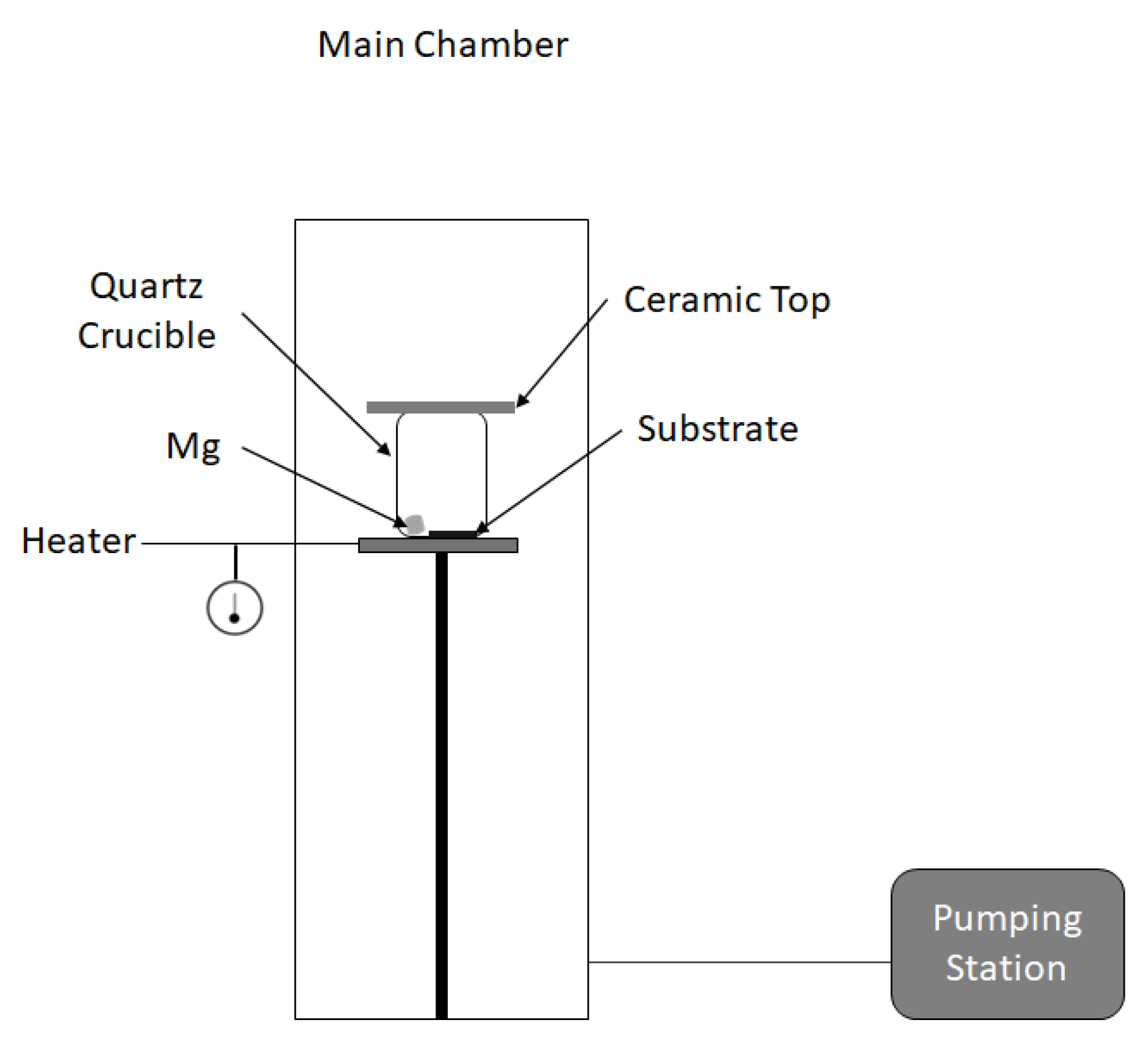
Abstract
:1. Introduction
2. Experimental Setup
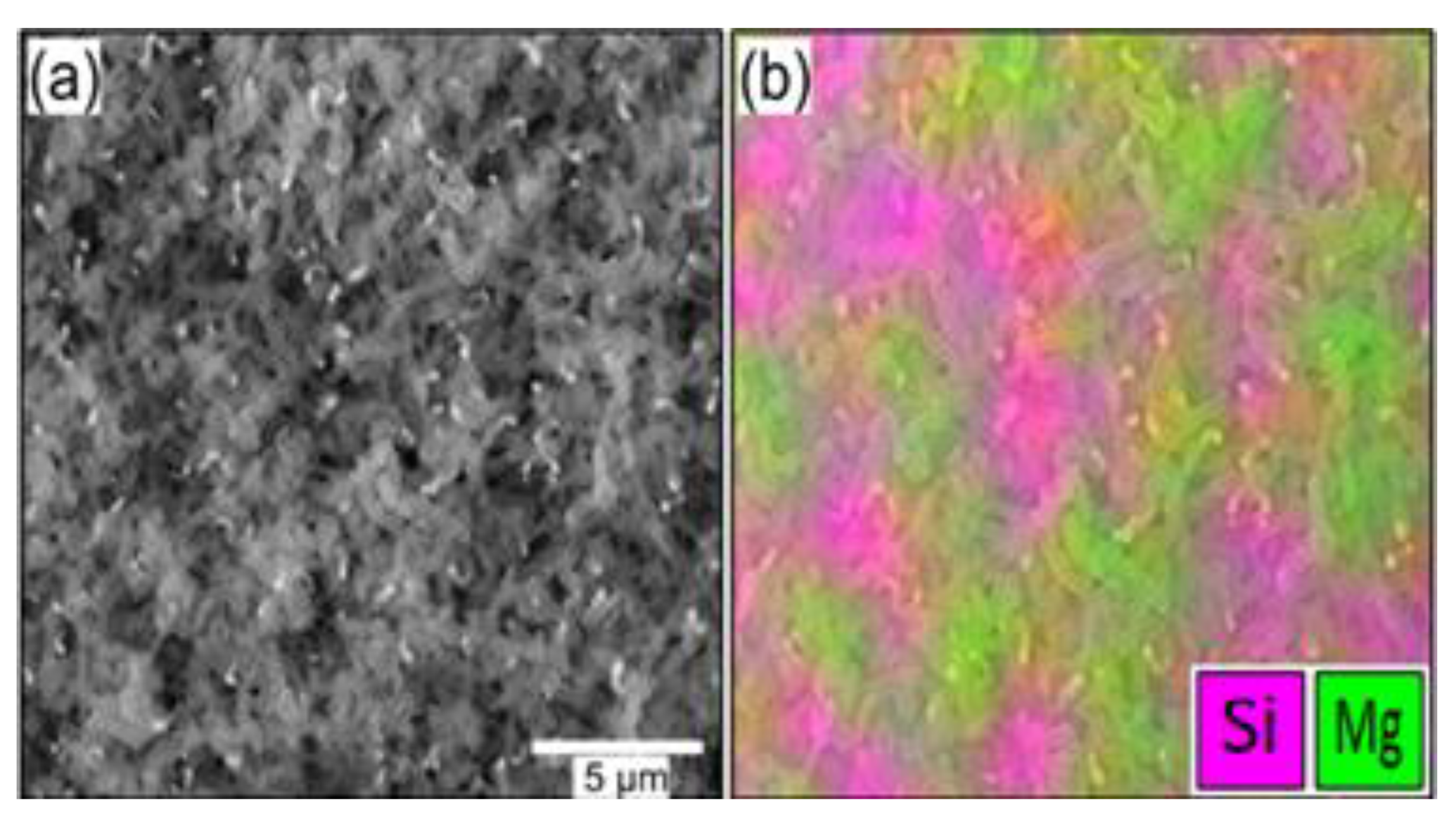
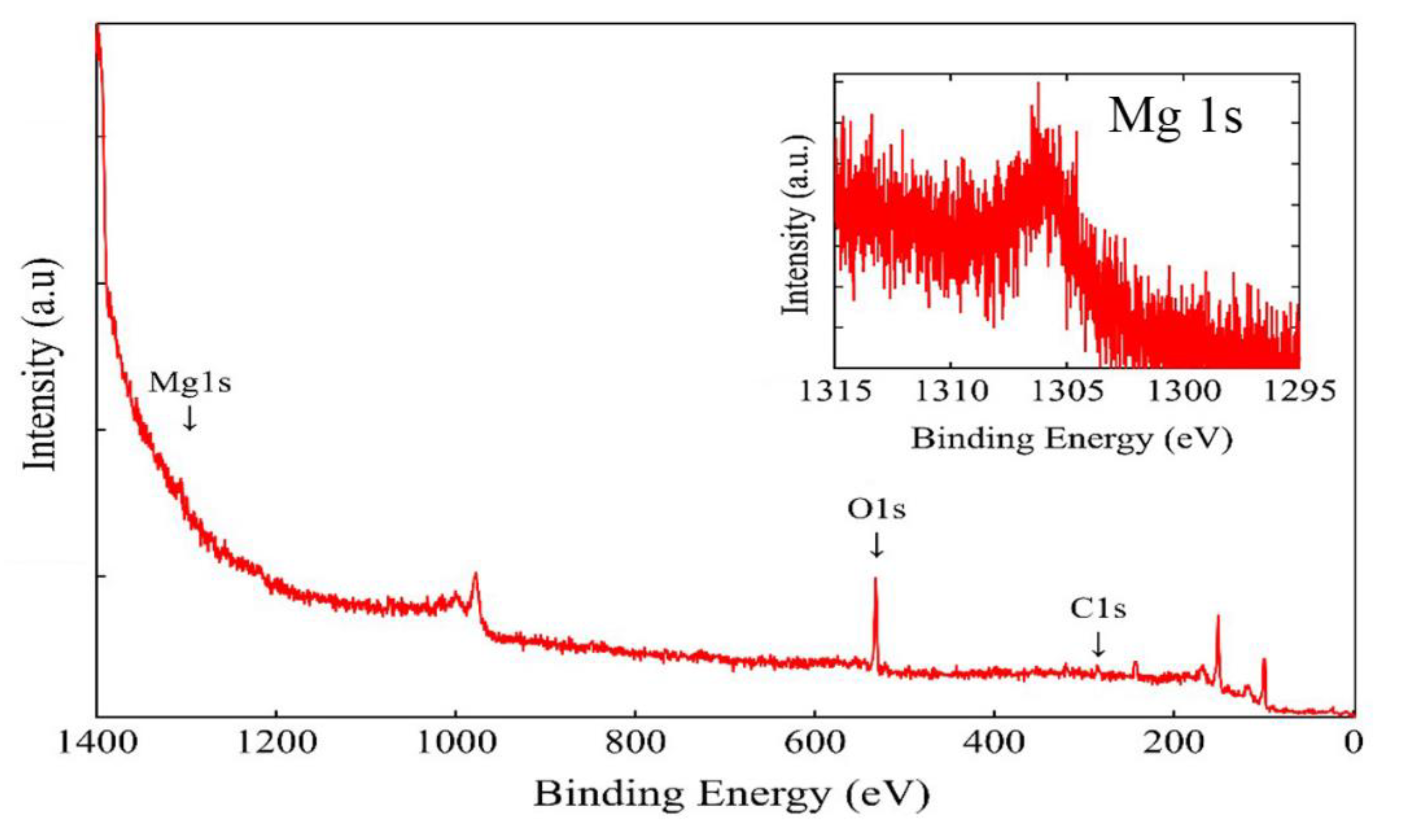
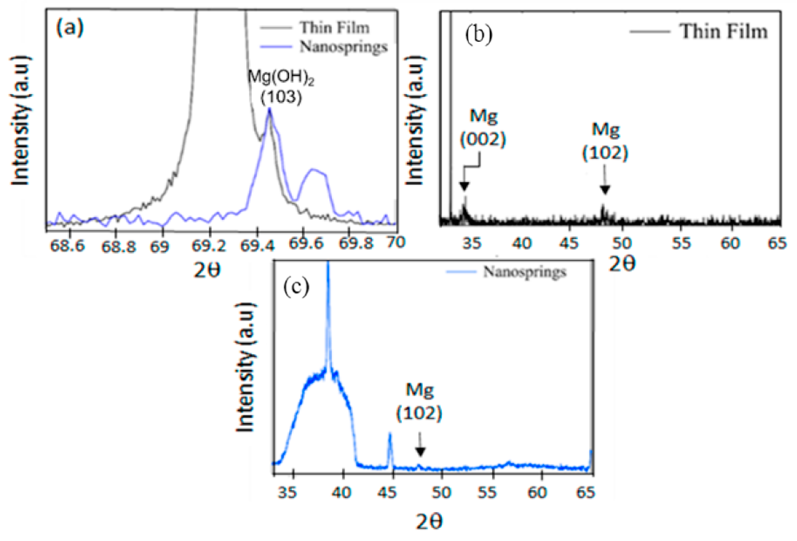
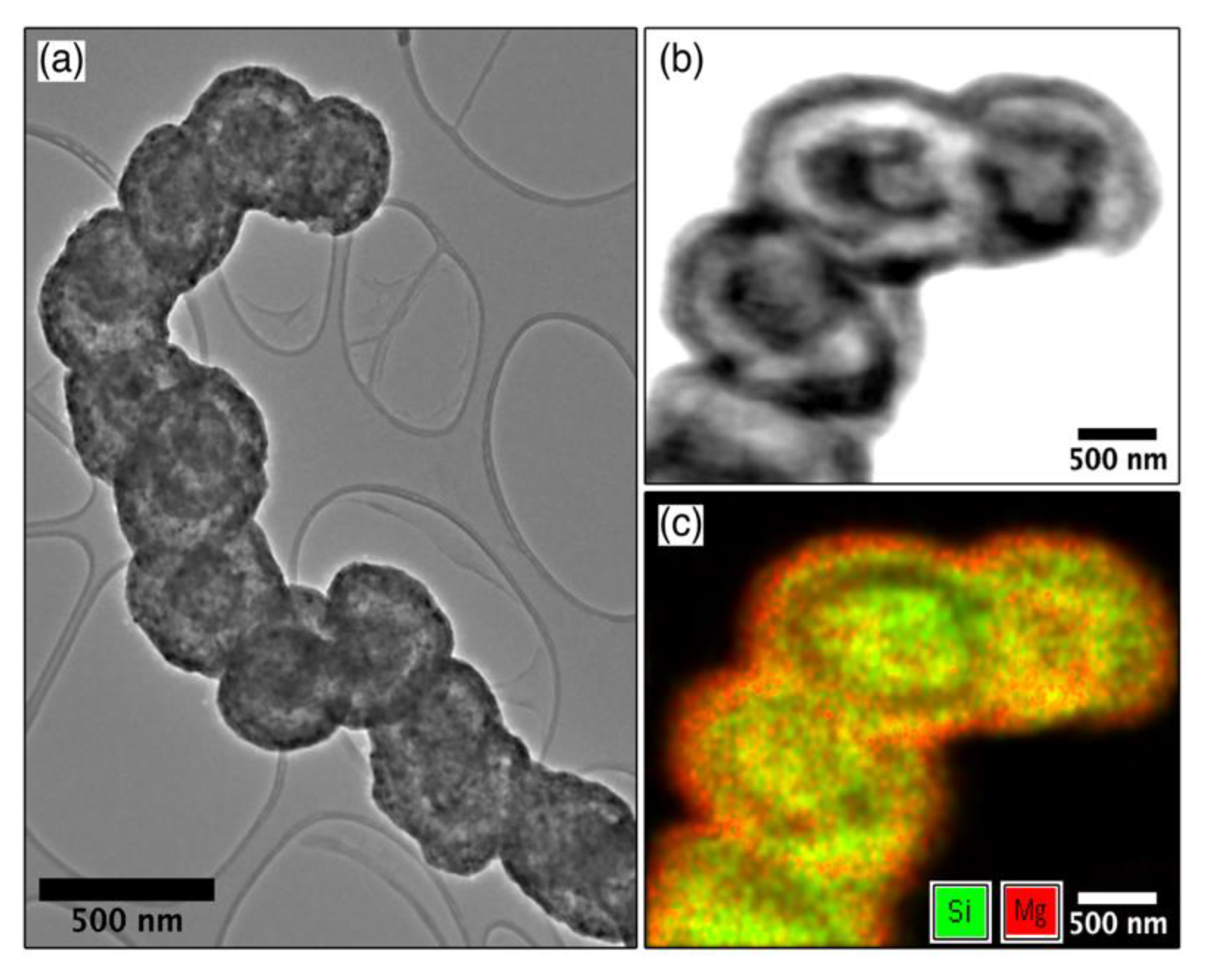
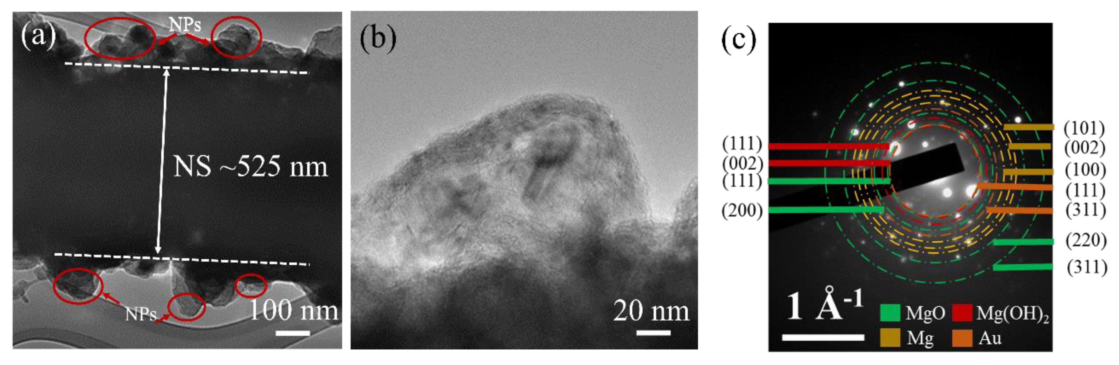
3. Materials Analysis
4. Results and Discussion
5. Conclusions
Author Contributions
Funding
Data Availability Statement
Acknowledgments
Conflicts of Interest
References
- Wang, L.; Li, J.; Wang, Y.; Yu, L.; Tang, X.; Zhang, Y.; Wang, S.; Wei, C. Construction of 1D SnO2-coated ZnO nanowire heterojunction for their improved n-butylamine sensing performances. Sci. Rep. 2016, 6, 35079. [Google Scholar] [CrossRef] [PubMed] [Green Version]
- Guo, J.; Zhang, J.; Zhu, M.; Ju, D.; Xu, H.; Cao, B. High-performance gas sensor based on ZnO nanowires functionalized by Au nanoparticles. Sens. Actuators B Chem. 2014, 199, 339–345. [Google Scholar] [CrossRef]
- Kong, B.H.; Choi, M.K.; Cho, H.K.; Kim, J.H.; Baek, S.; Lee, J.-H. Conformal Coating of Conductive ZnO:Al Films as Transparent Electrodes on High Aspect Ratio Si Microrods. Electrochem. Solid-State Lett. 2009, 13, K12. [Google Scholar] [CrossRef]
- Lin, S.; Wang, H.; Zhang, X.; Wang, D.; Zu, D.; Song, J.; Liu, Z.; Huang, Y.; Huang, K.; Tao, N.; et al. Direct spray-coating of highly robust and transparent Ag nanowires for energy saving windows. Nano Energy 2019, 62, 111–116. [Google Scholar] [CrossRef]
- Zhi, J.; Zhao, W.; Liu, X.; Chen, A.; Liu, Z.; Huang, F. Highly Conductive Ordered Mesoporous Carbon Based Electrodes Decorated by 3D Graphene and 1D Silver Nanowire for Flexible Supercapacitor. Adv. Funct. Mater. 2014, 24, 2013–2019. [Google Scholar] [CrossRef]
- Rajabi, N.; Wojcik, P.M.; Khanal, L.R.; Qiang, Y.; McIlroy, D.N. A comparison of the morphological and electrical properties of sol-gel dip coating and atomic layer deposition of ZnO on 3D nanospring mats. Mater. Res. Express 2018, 6, 035902. [Google Scholar] [CrossRef]
- Liang, H.-W.; Liu, S.; Yu, S.-H. Controlled Synthesis of One-Dimensional Inorganic Nanostructures Using Pre-Existing One-Dimensional Nanostructures as Templates. Adv. Mater. 2010, 22, 3925–3937. [Google Scholar] [CrossRef]
- Xia, Y.; Yang, P.; Sun, Y.; Wu, Y.; Mayers, B.; Gates, B.; Yin, Y.; Kim, F.; Yan, H. One-Dimensional Nanostructures: Synthesis, Characterization, and Applications. Adv. Mater. 2003, 15, 353–389. [Google Scholar] [CrossRef]
- Qiu, J.; Yu, W.; Gao, X.; Li, X. Sol–gel assisted ZnO nanorod array template to synthesize TiO2 nanotube arrays. Nanotechnology 2006, 17, 4695–4698. [Google Scholar] [CrossRef]
- Meng, X.; Banis, M.N.; Geng, D.; Li, X.; Zhang, Y.; Li, R.; Abou-Rachid, H.; Sun, X. Controllable atomic layer deposition of one-dimensional nanotubular TiO2. Appl. Surf. Sci. 2013, 266, 132–140. [Google Scholar] [CrossRef]
- Dvorak, F.; Zazpe, R.; Krbal, M.; Sopha, H.; Prikryl, J.; Ng, S.; Hromadko, L.; Bures, F.; Macak, J.M. One-dimensional anodic TiO2 nanotubes coated by atomic layer deposition: Towards advanced applications. Appl. Mater. Today 2019, 14, 1–20. [Google Scholar] [CrossRef]
- Marichy, C.; Bechelany, M.; Pinna, N. Atomic Layer Deposition of Nanostructured Materials for Energy and Environmental Applications. Adv. Mater. 2012, 24, 1017–1032. [Google Scholar] [CrossRef] [PubMed]
- Knez, M.; Nielsch, K.; Niinistö, L. Synthesis and Surface Engineering of Complex Nanostructures by Atomic Layer Deposition. Adv. Mater. 2007, 19, 3425–3438. [Google Scholar] [CrossRef]
- Chaaya, A.; Bechelany, M.; Balme, S.; Miele, P. ZnO 1D nanostructures designed by combining atomic layer deposition and electrospinning for UV sensor applications. J. Mater. Chem. A 2014, 2, 20650–20658. [Google Scholar] [CrossRef]
- Duan, X.; Liu, N. Magnesium for Dynamic Nanoplasmonics. Acc. Chem. Res. 2019, 52, 1979–1989. [Google Scholar] [CrossRef] [Green Version]
- Ringe, E. Shapes, Plasmonic Properties, and Reactivity of Magnesium Nanoparticles. J. Phys. Chem. C Nanomater. Interfaces 2020, 124, 15665–15679. [Google Scholar] [CrossRef]
- Biggins, J.S.; Yazdi, S.; Ringe, E. Magnesium Nanoparticle Plasmonics. Nano Lett. 2018, 18, 3752–3758. [Google Scholar] [CrossRef]
- Jain, P.; Lal, C.; Jain, A. Hydrogen storage in Mg: A most promising material. Int. J. Hydrogen Energy 2010, 35, 5133–5144. [Google Scholar] [CrossRef]
- Luo, Q.; Li, J.; Li, B.; Liu, B.; Shao, H.; Li, Q. Kinetics in Mg-based hydrogen storage materials: Enhancement and mechanism. J. Magnes. Alloys 2019, 7, 58–71. [Google Scholar] [CrossRef]
- Shao, H.; Xin, G.; Zheng, J.; Li, X.; Akiba, E. Nanotechnology in Mg-based materials for hydrogen storage. Nano Energy 2012, 1, 590–601. [Google Scholar] [CrossRef]
- Gupta, M.; Ling, S.N.M. Magnesium, Magnesium Alloys, and Magnesium Composites; John Wiley & Sons: Hoboken, NJ, USA, 2011. [Google Scholar]
- Duan, X.; Yue, S.; Liu, N. Understanding complex chiral plasmonics. Nanoscale 2015, 7, 17237–17243. [Google Scholar] [CrossRef] [PubMed]
- Mohammadi, E.; Tsakmakidis, K.L.; Askarpour, A.N.; Dehkhoda, P.; Tavakoli, A.; Altug, H. Nanophotonic Platforms for Enhanced Chiral Sensing. ACS Photonics 2018, 5, 2669–2675. [Google Scholar] [CrossRef]
- Duan, X.; Kamin, S.; Sterl, F.; Giessen, H.; Liu, N. Hydrogen-Regulated Chiral Nanoplasmonics. Nano Lett. 2016, 16, 1462–1466. [Google Scholar] [CrossRef] [PubMed]
- Jeong, H.-H.; Mark, A.G.; Fischer, P. Magnesium plasmonics for UV applications and chiral sensing. Chem. Commun. 2016, 52, 12179–12182. [Google Scholar] [CrossRef] [Green Version]
- Sterl, F.; Strohfeldt, N.; Walter, R.; Griessen, R.; Tittl, A.; Giessen, H. Magnesium as Novel Material for Active Plasmonics in the Visible Wavelength Range. Nano Lett. 2015, 15, 7949–7955. [Google Scholar] [CrossRef]
- Gutiérrez, Y.; de la Osa, R.A.; Ortiz, D.; Saiz, J.; González, F.; Moreno, F. Plasmonics in the Ultraviolet with Aluminum, Gallium, Magnesium and Rhodium. Appl. Sci. 2018, 8, 64. [Google Scholar] [CrossRef] [Green Version]
- Arrowsmith, M.; Hill, M.S.; Kociok-Köhn, G. Magnesium Catalysis of Imine Hydroboration. Chem. Eur. J. 2013, 19, 2776–2783. [Google Scholar] [CrossRef]
- Yang, D.; Wang, L.; Li, D.; Wang, R. Magnesium Catalysis in Asymmetric Synthesis. Chem 2019, 5, 1108–1166. [Google Scholar] [CrossRef]
- Froes, F.H.; Eliezer, D.; Aghion, E. The science, technology, and applications of magnesium. JOM 1998, 50, 30–34. [Google Scholar] [CrossRef]
- Knight, L.B.; Brittain, R.D.; Duncan, M.; Joyner, C.H. Unusual behavior of vaporized magnesium under low pressure conditions. J. Phys. Chem. 1975, 79, 1183–1190. [Google Scholar] [CrossRef]
- Uddin, G.M.; Ziemer, K.S.; Zeid, A.; Lee, Y.-T.T.; Kamarthi, S. Process control model for growth rate of molecular beam epitaxy of MgO (111) nanoscale thin films on 6H-SiC (0001) substrates. Int. J. Adv. Manuf. Technol. 2017, 91, 907–916. [Google Scholar] [CrossRef]
- Song, J.-G.; Park, J.; Yoon, J.; Woo, H.; Ko, K.; Lee, T.; Hwang, S.-H.; Myoung, J.-M.; Kim, K.; Jang, Y.; et al. Plasma enhanced atomic layer deposition of magnesium oxide as a passivation layer for enhanced photoluminescence of ZnO nanowires. J. Lumin. 2014, 145, 307–311. [Google Scholar] [CrossRef]
- Herman, M.A.; Sitter, H. Molecular Beam Epitaxy: Fundamentals and Current Status; Springer Science & Business Media: Berlin/Heidelberg, Germany, 2012. [Google Scholar]
- Wang, L.; Major, D.; Paga, P.; Zhang, D.; Norton, M.G.; McIlroy, D.N. High yield synthesis and lithography of silica-based nanospring mats. Nanotechnology 2006, 17, S298–S303. [Google Scholar] [CrossRef]
- Corti, G.; Brown, J.; Rajabi, N.; McIlroy, D.N. Threefold growth efficiency improvement of silica nanosprings by using silica nanosprings as a substrate. Nanotechnology 2018, 29, 115604. [Google Scholar] [CrossRef] [PubMed]
- Wojcik, P.M.; Bakharev, P.V.; Corti, G.; McIlroy, D.N. Nucleation, evolution, and growth dynamics of amorphous silica nanosprings. Mater. Res. Express 2017, 4, 015004. [Google Scholar] [CrossRef]
- McIlroy, D.N.; Zhang, D.; Kranov, Y.; Norton, M.G. Nanosprings. Appl. Phys. Lett. 2001, 79, 1540. [Google Scholar] [CrossRef]
- Corneille, S.; He, J.-W.; Goodman, D.W. XPS characterization of ultra-thin MgO films on a Mo(100) surface. Surf. Sci. 1994, 306, 269–278. [Google Scholar] [CrossRef]
- Wang, J.A.; Novaro, O.; Bokhimi, X.; López, T.; Gómez, R.; Navarrete, J.; Llanos, M.E.; López-Salinas, E. Characterizations of the thermal decomposition of brucite prepared by sol–gel technique for synthesis of nanocrystalline MgO. Mater. Lett. 1998, 35, 317–323. [Google Scholar] [CrossRef]
- Nied, D.; Enemark-Rasmussen, K.; L’Hopital, E.; Skibsted, J.; Lothenbach, B. Properties of magnesium silicate hydrates (M-S-H). Cem. Concr. Res. 2016, 79, 323–332. [Google Scholar] [CrossRef]
- Schmiesing, N.C.; Corti, G.; Sommers, A.D. Water Condensation and Droplet Shedding Behavior on Silica-Nanospring-Coated Tubes. ACS Appl. Mater. Interfaces 2020, 12, 17046–17054. [Google Scholar] [CrossRef]
- Morita, M.; Ohmi, T.; Hasegawa, E.; Kawakami, M.; Ohwada, M. Growth of native oxide on a silicon surface. J. Appl. Phys. 1990, 68, 1272–1281. [Google Scholar] [CrossRef]
- Brichni, A.; Hammi, H.; Aggoun, S.; Mnif, A. Optimisation of magnesium oxychloride cement properties by silica glass. Adv. Cem. Res. 2016, 28, 654–663. [Google Scholar] [CrossRef]
- Paik, B.; Jones, I.P.; Walton, A.; Mann, V.; Book, D.; Harris, I.R. MgH2 → Mg phase transformation driven by a high-energy electron beam: An in situ transmission electron microscopy study. Philos. Mag. Lett. 2010, 90, 1–7. [Google Scholar] [CrossRef]
- Persson, K. Materials Data on Mg (SG:194) by Materials Project. 2015. [CrossRef]
- Persson, K. Materials Data on MgO (SG:225) by Materials Project. 2014. [CrossRef]
- Kim, G.; Dahmen, U.; Searcy, A.W. Structural Transformations in the Decomposition of Mg(OH)2 and MgCO3. J. Am. Ceram. Soc. 1987, 70, 146–154. [Google Scholar] [CrossRef]
- Austin, J.; Echeverria, E.; Wagle, P.; Mainali, P.; Meyers, D.; Gupta, A.K.; Sachan, R.; Prassana, S.; McIlroy, D.N. High-Temperature Atomic Layer Deposition of GaN on 1D Nanostructures. Nanomaterials 2020, 10, 2434. [Google Scholar] [CrossRef] [PubMed]


Publisher’s Note: MDPI stays neutral with regard to jurisdictional claims in published maps and institutional affiliations. |
© 2022 by the authors. Licensee MDPI, Basel, Switzerland. This article is an open access article distributed under the terms and conditions of the Creative Commons Attribution (CC BY) license (https://creativecommons.org/licenses/by/4.0/).
Share and Cite
Austin, A.J.; Dice, N.P.; Echeverria, E.; Gupta, A.K.; Risner, J.; Helfrich, H.C.; Sachan, R.; McIlroy, D.N. Magnesium Sublimation for Growing Thin Films and Conformal Coatings on 1D Nanostructures. Nanomanufacturing 2022, 2, 186-193. https://doi.org/10.3390/nanomanufacturing2040013
Austin AJ, Dice NP, Echeverria E, Gupta AK, Risner J, Helfrich HC, Sachan R, McIlroy DN. Magnesium Sublimation for Growing Thin Films and Conformal Coatings on 1D Nanostructures. Nanomanufacturing. 2022; 2(4):186-193. https://doi.org/10.3390/nanomanufacturing2040013
Chicago/Turabian StyleAustin, Aaron J., Nathan P. Dice, Elena Echeverria, Ashish Kumar Gupta, Jonathan Risner, Halle C. Helfrich, Ritesh Sachan, and David N. McIlroy. 2022. "Magnesium Sublimation for Growing Thin Films and Conformal Coatings on 1D Nanostructures" Nanomanufacturing 2, no. 4: 186-193. https://doi.org/10.3390/nanomanufacturing2040013