Article

Enhancement of Photo-Electrical Properties of CdS Thin Films: Effect of N2 Purging and N2 Annealing

by
Gayan K. L. Sankalpa
1,2,
Gayan R. K. K. G. R. Kumarasinghe
1,2,
Buddhika S. Dassanayake
1,2 and
Gayan W. C. Kumarage
3,*
1
Postgraduate Institute of Science, University of Peradeniya, Peradeniya 20400, Sri Lanka
2
Department of Physics, Faculty of Science, University of Peradeniya, Peradeniya 20400, Sri Lanka
3
Department of Physics and Electronics, Faculty of Science, University of Kelaniya, Kelaniya 11600, Sri Lanka
*
Author to whom correspondence should be addressed.
Electron. Mater. 2024, 5(1), 30-44; https://doi.org/10.3390/electronicmat5010003
Submission received: 17 January 2024 / Revised: 19 February 2024 / Accepted: 11 March 2024 / Published: 13 March 2024
(This article belongs to the Topic Optoelectronic Materials, 2nd Volume)

Abstract

:
The impact of N2 purging in the CdS deposition bath and subsequent N2 annealing is examined and contrasted with conventional CdS films, which were deposited without purging and annealed in ambient air. All films were fabricated using the chemical bath deposition method at a temperature of 80 °C on fluorine-doped tin oxide glass slides (FTO). N2 purged films were deposited by introducing nitrogen gas into the deposition bath throughout the CdS deposition process. Subsequently, both N2 purged and un-purged films underwent annealing at temperatures ranging from 100 to 500 °C for one hour, either in a nitrogen or ambient air environment. Photoelectrochemical (PEC) cell studies reveal that films subjected to both N2 purging and N2 annealing exhibit a notable enhancement of 37.5% and 27% in ISC (short-circuit current) and VOC (open-circuit voltage) values, accompanied by a 5% improvement in optical transmittance compared to conventional CdS thin films. The films annealed at 300 °C demonstrate the highest ISC, VOC, and VFB values, 55 μA, 0.475 V, and −675 mV, respectively. The improved optoelectrical properties in both N2-purged and N2-annealed films are attributed to their well-packed structure, enhanced interconnectivity, and a higher sulfur to cadmium ratio of 0.76 in the films.

1. Introduction

CdS is a common choice for the “window layer” of CdTe heterojunction solar cells. Thanks to the large and direct bandgap (2.42 eV) of CdS, the majority of the solar spectrum is transmitted rather easily, making CdS an appropriate window layer above the CdTe absorber in which photogeneration of excess minority carriers takes place [1]. There are many deposition techniques for CdS thin-film deposition [2]. These deposition techniques are either purely physical or purely chemical or a combination of both [1]. Among different methods of CdS deposition, the chemical bath deposition (CBD) method emerges as a simple and economical technique to grow high quality thin films for large-area deposition [3,4].
The properties of CdS thin films, along with many other binary metal chalcogenides produced through CBD, are significantly influenced by various growth parameters. These parameters include the concentrations of metal and chalcogenide ions, pH of the chemical bath, deposition temperature, duration of deposition, and the oxygen percentage in the solution [5]. The pH level of the bath has been documented to cause changes in both grain size and optical bandgap of CdS films [6]. Moreover, the temperature of the chemical bath can impact the grain size, subsequently affecting the effective surface area [7]. Numerous studies in the literature have extensively discussed the influence of the bath temperature on the optoelectronic properties of CBD-CdS deposited films [8,9]. Furthermore, it is suggested that bath temperature and deposition duration may play a crucial role in adjusting the film thickness and growth rate of CdS films [10].
It is known that thermal annealing at the proper temperature is crucial to improve the thin-film crystallinity and hence the electrical properties of CdS thin films [11,12]. Furthermore, annealing CdS films under a hydrogen or nitrogen environment decreases the resistivity as a result of increased electron density [13]. Also, annealing treatments can modify the morphology of the film, which in turn alters the optical properties [14]. The possibility of alteration of relative band position, and hence, the Fermi levels of CdS depending on the different annealing environments such as Ar + H2, Ar + S, Ar + CdCl2 and O2 has also been reported [15].
In the reporting work, the preparative procedure of the conventional CdS films has been altered with the purging of N2 gas into the deposition bath followed by post-deposition N2 annealing, potentially improving the uniformity and homogeneity of the films deposited. The structural, morphological, electrical, and optical properties of the deposited films are discussed using respective characterization techniques to assess the effectiveness of the deposition mechanism proposed for CdS.

2. Materials and Methods

The fluorine doped tin oxide (FTO, Sigma-Aldrich, St. Louis, MO, USA) glass substrates were first washed with detergent and running de-ionized (DI) water before ultrasound sonication. Later, glass substrates were cleaned following a method described elsewhere [8,15,16,17].
During the deposition, cleaned FTO glasses were placed inside a beaker at an angle of 45° to the horizontal using a homemade sample holder. The chemical bath deposition was performed in a reaction solution consisting of 10 mL of 0.01 mol.dm−3 cadmium sulphate (3CdSO4.8H2O, 99%, Breckland Scientific, Stafford, UK), 1.1 mL of ammonia solution (NH3, 5% w/w, Surechem Products Ltd., Ipswich, UK), and 118.9 mL of DI water, while 10 mL of 0.02 mol.dm−3 thiourea (CS(NH2)2, 99%, MRS Scientific Inc., Wickford, UK) was added drop by drop for 1 h into the reaction solution. Magnetic stirring (200 rpm) was utilized for a homogeneous growth of CdS [18,19].
N2 purged films were deposited by bubbling N2 into the reaction solution over the course of CdS deposition process. Prior to deposition, the chemical solution was N2 purged for more than 30 min at a high bubbling rate of (200 bubbles per minute, 3000 standard cubic centimeters, sccm). During the deposition of CdS, N2 flow rate was slow, and it was set to 100 bubbles per minute (1500 sccm) to eliminate agitation by the gas flux during the growth of CdS. Both the N2 purged and un-purged films were later annealed at 100, 200, 300, 400, and 500 °C in BüchiTo-51 tube furnace for one hour. Employing the deposition and annealing methodologies outlined above, we fabricated four distinct CdS film variants to systematically examine their optical, electrical, compositional, morphological, and structural attributes. Table 1 provides details regarding the deposited films.

2.1. Chemical Reaction Route

The formation of CBD-CdS has been discussed by many researchers [20,21,22,23]. The reaction route initiates with the hydrolysis of ammonia in the water giving out OH;
NH3 + H2O ↔ NH4+ + OH
Then, CdSO4 begins to dissolve as follows,
CdSO4 → Cd2+ + SO42−
The above Equation (1) makes the medium basic with a pH of about 11. The sulfur source, thiourea, which is added drop by drop throughout, then hydrolyzes in alkaline solution to give S2−.
CS(NH2)2 + 2OH ↔ S2− + CN2H2 + 2H2O
The CdS deposition mechanism is known to be two-fold, depending on the bath temperature at which the deposition occurs. At low temperatures, deposition is through the “ion-by-ion” mechanism, which is given by the reaction route.
Cd2+ + S2−→ CdS↓
At higher temperatures, the deposition is through a “cluster-by-cluster” mechanism. There, Cd2+ reacts in the basic medium as in Equations (5)–(7).
Cd2+ + 2OH ↔ Cd(OH)2
nCd(OH)2 + nS2− ↔ (CdS)n↓ + 2nOH
Cd(OH)2 + 4NH4OH ↔ [Cd(NH3)4]2+ + 4H2O + 2OH
Finally, [Cd(NH3)4]2+ and sulfide ions react to form CdS.
[Cd(NH3)4]2+ + S2− ↔ (CdS)n↓ + 4NH3
Since the concentration of [Cd(NH3)4]2+ is not rich enough to hinder the growth of Cd(OH)2, a small amount of Cd(OH)2 could be precipitated. Subsequently, CdS is deposited by the gradually generated S2− ion as in Equation (6) [24].
In the reporting work, all the depositions were conducted at 80 °C, where the cluster-by-cluster deposition mechanism is encouraged. All the deposited films were about 80 nm in thickness.

2.2. Characterizations

The I-V measurements were carried out using the photoelectrochemical (PEC) cell with configuration FTO/CdS/0.1 mol.dm−3 Na2S2O3/Pt using PEC Cell L01 solar simulator with Keithley 2400 series source meter. The cell area was 0.25 cm2, and the CdS/electrolyte junction was irradiated using a 150 W Xenon lamp. C-V measurements were conducted within the potential window from −0.8 to +0.4 V for the PEC Cell configuration described above using Gamry potentiostat G-300 at a frequency of 1000 Hz. Ag/AgCl and a Pt plate were used as the reference and counter and electrode, respectively, for all the PEC characterizations. UV-vis spectrophotometric measurements of films in both transmittance and absorbance modes were obtained from double-beam UV-vis spectrophotometer (UV-1800 Shimadzu) in the optical window from 300 to 800 nm. The morphology of the films was observed by SEM images using Zeiss EVO|LS15 SEM, while the composition was assessed using Energy Dispersive X-ray (EDX) by INCA X-act SN 67217 EDX under an accelerating voltage of 10 keV. The thickness of the grown films was measured by using the SEM cross-section images. The surface roughness was investigated using a Veeco Atomic Force Microscope (AFM, model 840-017-900R). Grazing Incidence X-ray Diffraction (GIXRD) was carried out by using a PANalytical X-ray diffractometer.

3. Results and Discussion

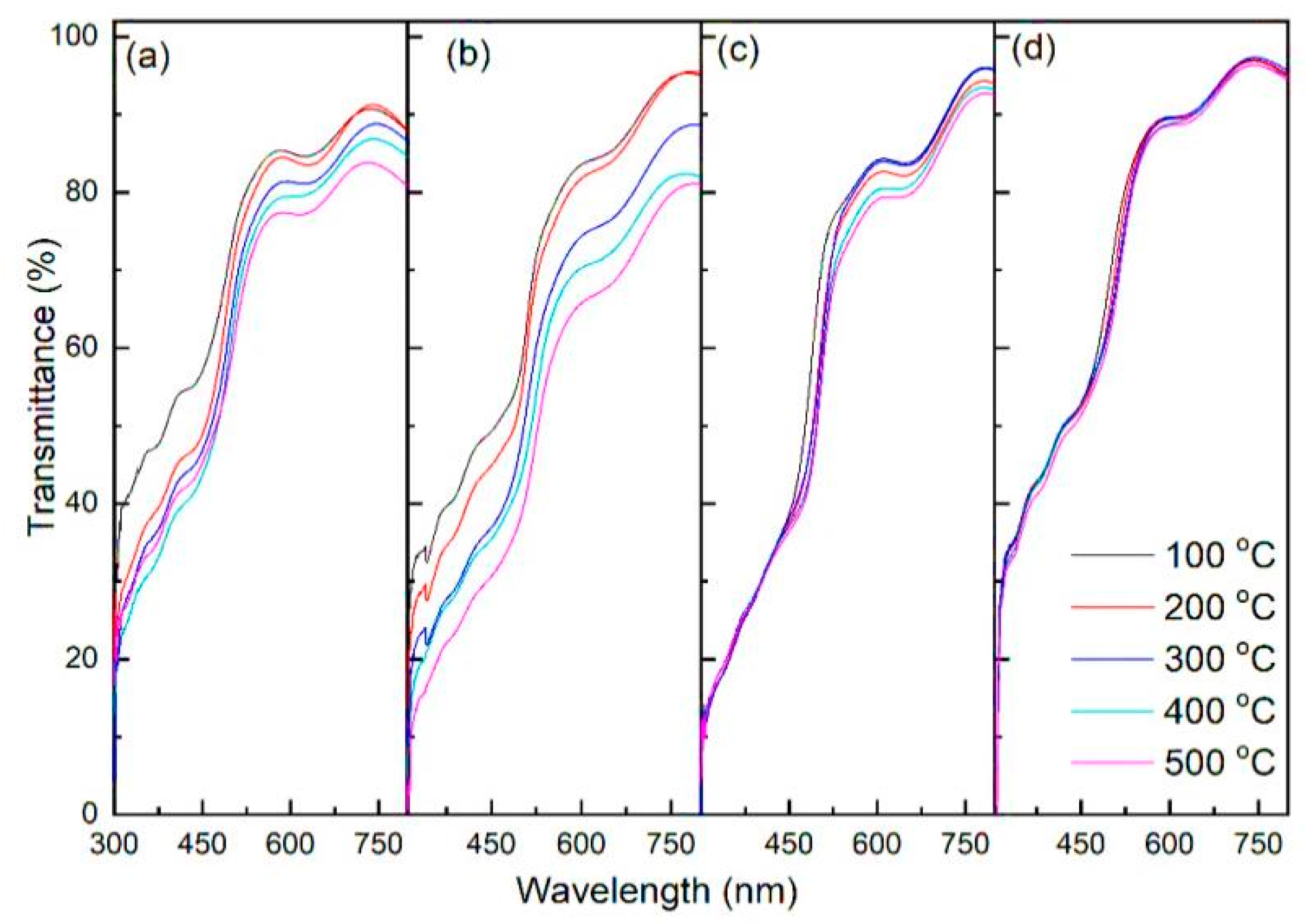
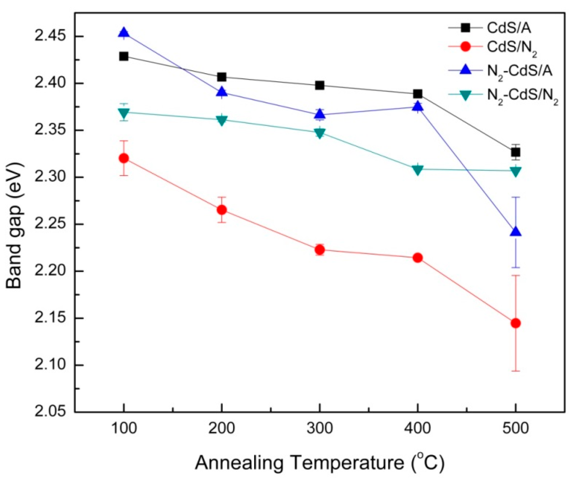
3.1. Optical Properties

The optical transmittance spectra of the grown thin films are shown in Figure 1. According to Figure 1, the optical transmittance of all the grown films was found to reduce with increasing annealing temperature. It is evident from Figure 1 that the transmittance edges of almost all the N2 unpurged films are subjected to a red shift with the increasing annealing temperature. However, all the N2 purged films showed almost identical transmittance behavior irrespective of the annealing temperature. Additionally, it was noted that the average transmittance values of all the films are greater than 80% in the wavelength range of 600 to 900 nm, and N2-CdS/N2 has the highest optical transmittance out of all the films deposited. The optical transmittance in the visible region depends on crystal defects, dislocation density, and grain boundaries of the film [25]. Hence, optical transmittance results suggest a low density of defects and relatively higher crystal quality of the N2-CdS/N2 films compared to that of other films [18].
The optical band gap values (Eg) of the films were obtained by (αhυ)2 vs. hυ plots derived from Equation (9) [26,27].
α = A ( h ν E g ) n / 2 h ν
where A is a constant, h is Plank’s constant, and n is equal to 1 for direct bandgap materials such as CdS. The absorption coefficient (α) was calculated by using Lambert’s law, Equation (10) [28].
α d = ln ( I 0 I T ) = 2.303 Abs
where IT and I0 are intensities of transmittance and incidence radiation, respectively, Abs is the optical absorbance, and d is the thickness of the film [29]. The derived Eg values are plotted in Figure 2.
Figure 2 reveals that irrespective of the type of film, all of the samples are subjected to a reduction in Eg with the increasing annealing temperature. The highest decrement in Eg over the range of temperatures was observed for CdS/N2. The decrement in Eg with annealing temperature can be due to factors such as re-organization of the film, S evaporation, and self-oxidation [30].
Re-organizing the film is a common cause in all annealing temperatures. The re-organizing process is twofold: (a) the film becomes more orderly due to the filling of empty sites and (b) evaporation of absorbed water from the film. Filling up of voids encourages them to form denser films and hence a reduction in Eg. However, the second route may cause empty sites in the film due to the evaporation of absorbed water. It is also a known factor that S in the CdS films can be subjected to evaporation at temperatures higher than 375 °C, turning the yellowish film to brownish yellow [31]. S evaporation can also decrease the Eg of the annealed CdS film. Also, the self-oxidation process can occur, even if the film is annealed under N2 atmosphere due to a couple of possible oxidation agents. One of them is the absorbed/adsorbed water in the film from the bath solution, and the other is the remaining residues of Cd(OH)2 in the film. As a result, when the film is subjected to annealing, CdO can form through the following means.
Cd(OH)2 → CdO +H2O
This process can influence the decrease in Eg in two means: (a) the creation of CdO and (b) H2O formed during the process causing further oxidation of the film. Therefore, even with a small percentage of oxidation, a decrement in Eg is possible to observe.
Based on the findings, enhanced transparency of CdS films can be realized through the introduction of N2 purging into the CdS bath, coupled with subsequent annealing in a nitrogen environment. An additional crucial criterion for the production of highly efficient CdS/CdTe solar cells involves attaining elevated photoconductivity of CdS to mitigate electrical losses [25]. Hence, it is imperative to evaluate alterations in the electrical properties resulting from the application of nitrogen purging and annealing processes.

3.2. Electrical Properties

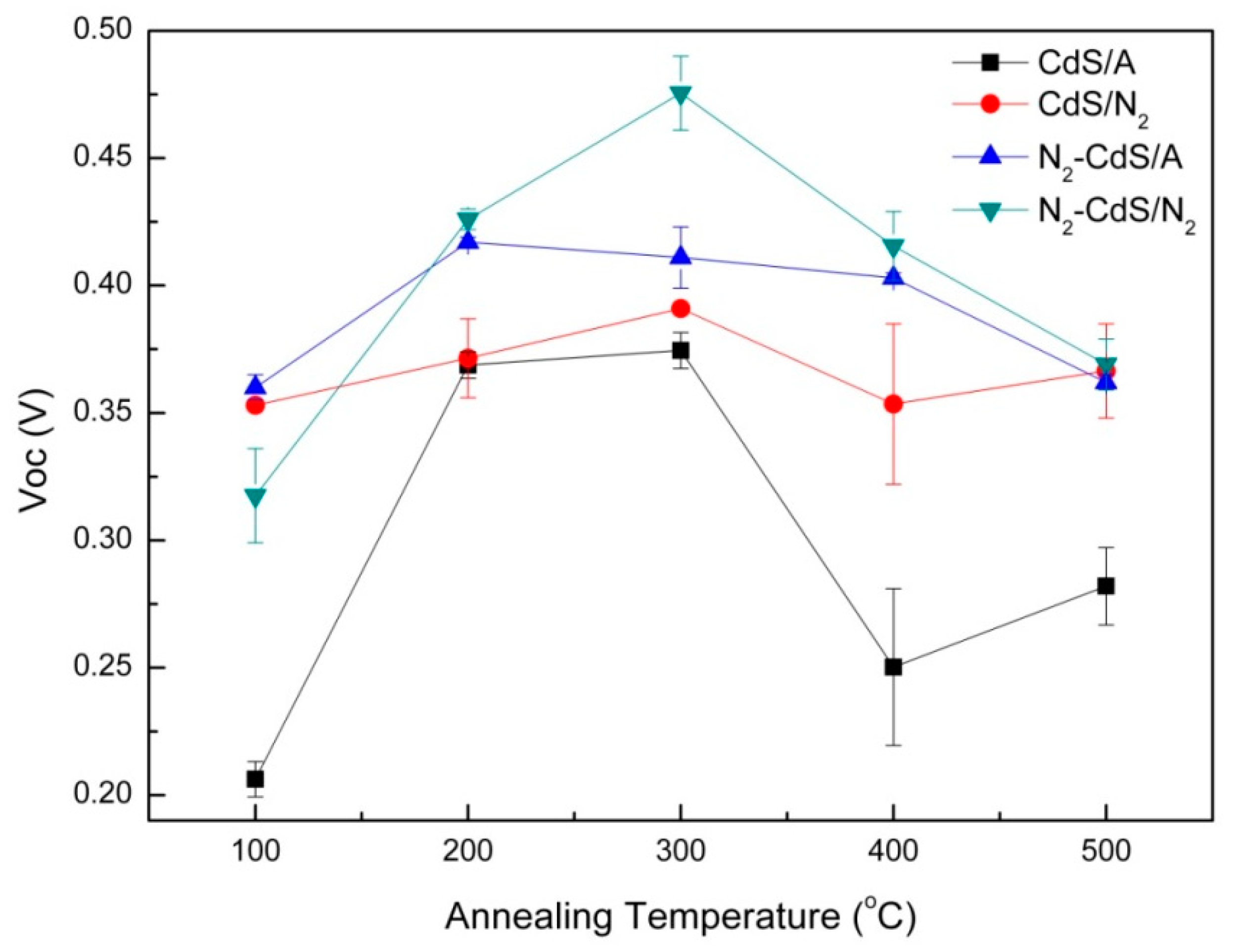
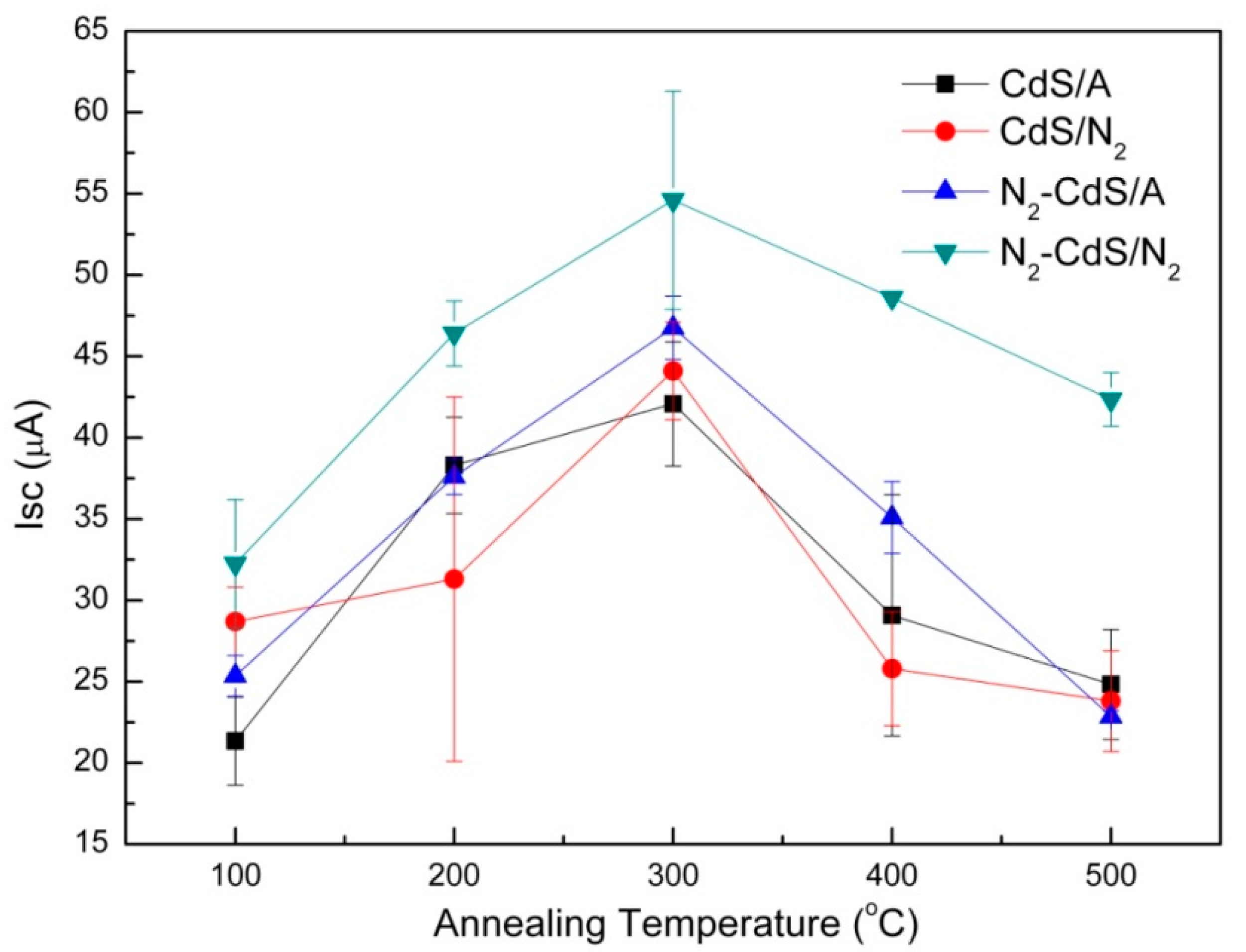
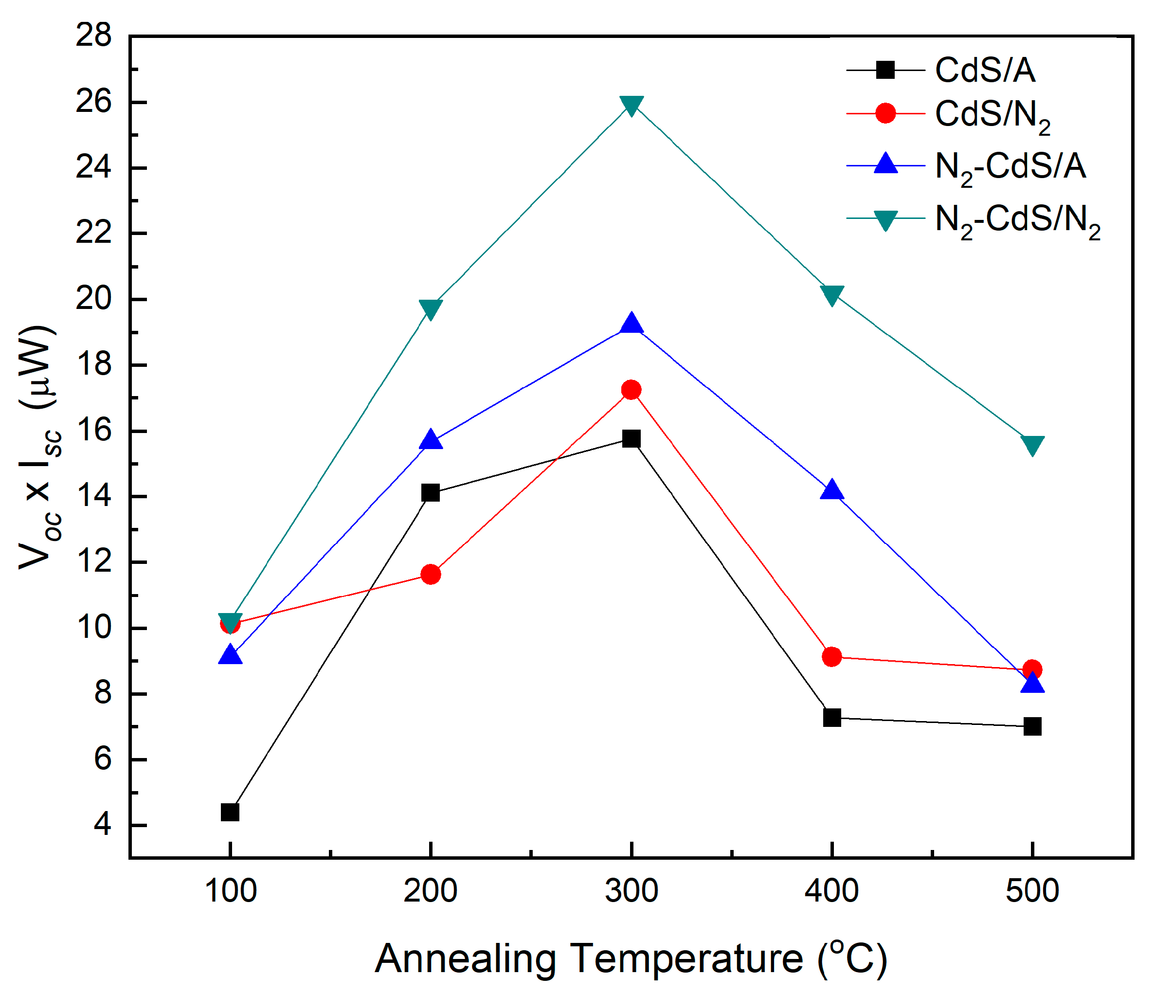
3.2.1. PEC Cell Analysis

The variation in VOC (open circuit voltage) in the PEC cell with respect to annealing temperature for all four types of films is given in Figure 3. According to the result, irrespective of the type of annealing followed, 300 °C seems to have produced the films with the highest VOC. Furthermore, film N2-CdS/N2 has shown the highest VOC at an annealing temperature of value 300 °C compared to the rest.
The variation in ISC (short circuit current) in the PEC cell with respect to different annealing temperatures for the four different types of films is shown in Figure 4. From the result, it is evident that all of the films show an initial increase in ISC before it starts decreasing beyond 300 °C, similar to the behavior of VOC. It is also observable that, out of the four different films, N2-CdS/N2 has shown higher ISC values at all of the annealing temperatures, with the highest ISC value recorded at an annealing temperature of 300 °C.
Figure 5 shows the variation in the ISC × VOC value in the PEC cell for all of the grown films. Due to the recorded high ISC and VOC values, the film N2-CdS/N2 results in the best ISC × VOC value compared to the rest, at any given annealing temperature. According to Figure 3, Figure 4 and Figure 5, it can be concluded that the PEC cell of the N2-CdS/N2 films results in higher ISC, VOC compared to the rest and hence exhibits superior photoconductivity.
It is a known fact that annealing improves the crystallinity of materials because it helps the motion of atoms to reach a stable position owing to thermal energy [32]. Therefore, an improvement in the crystallinity of the CdS films can be expected when the annealing temperature is increased, irrespective of the method of deposition and method of annealing. Therefore, improved electrical properties of the films up to an annealing temperature of 300 °C can be justified [33,34]. However, S can leave the CdS films when subjected to annealing temperatures greater than 375 °C. This effect can leave non-stoichiometric CdS films [31]. Small grain size, a lower degree of crystallinity, and the occurrence of defects such as surface imperfections, structural dislocations, and disorders lead to the sinking of electrical properties [35]. Evaporation of S from CdS films can also introduce a lower degree of crystallinity to the film and hence could be the reason for poor electrical properties observed at higher temperatures.

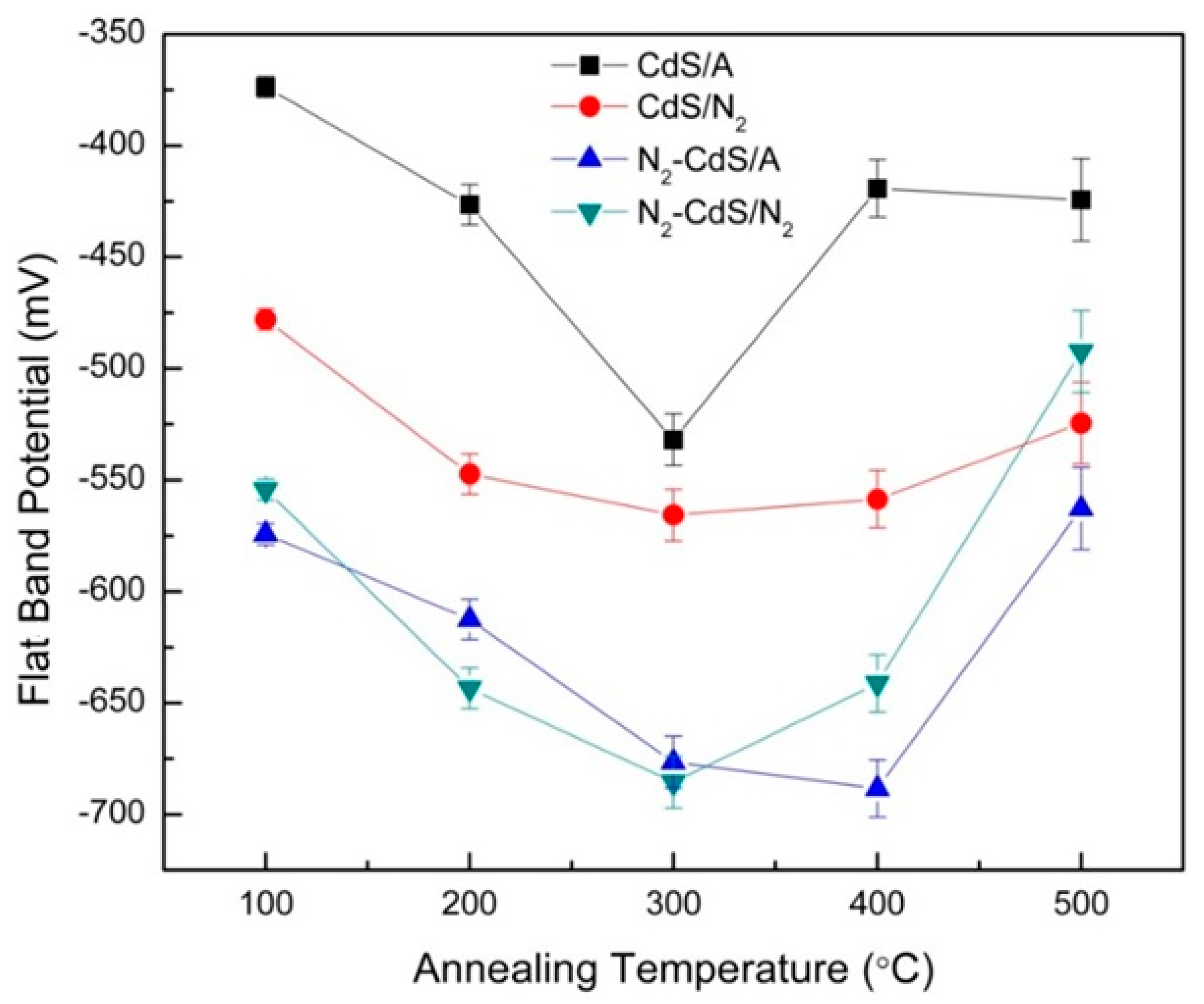
3.2.2. C—V Measurements

The VFB (flat band potential) value of all the grown films was calculated from the x-axis intercept of the linear fit of the Mott–Schottky equation [36]. The obtained VFB results are shown in Figure 6. The result confirms the n-type electrical character of all the CdS films which were annealed at different temperatures. According to the results, it is evident that both N2-CdS/N2 and N2-CdS/A films display higher VFB values compared to the rest, at any given annealing temperature. For the N2 purged films, an annealing temperature of 300–400 °C was found to produce the highest VFB values.
The previously observed enhancement in the VOC value irrespective of the growth method could be due to the higher VFB [24]. This tendency of variation is evidently seen in Figure 3 and Figure 6, where both VOC and the VFB show a similar trend of variation. The electrical properties of the grown films depend on surface morphology as well as the inter-particle connectivity [8,16,17,19]. Therefore, topological and structural characterizations were conducted for a better understanding of the variation in optoelectrical properties when subjected to N2 purging and annealing using the films annealed at 300 °C, which yielded the best electrical and optical characteristics.

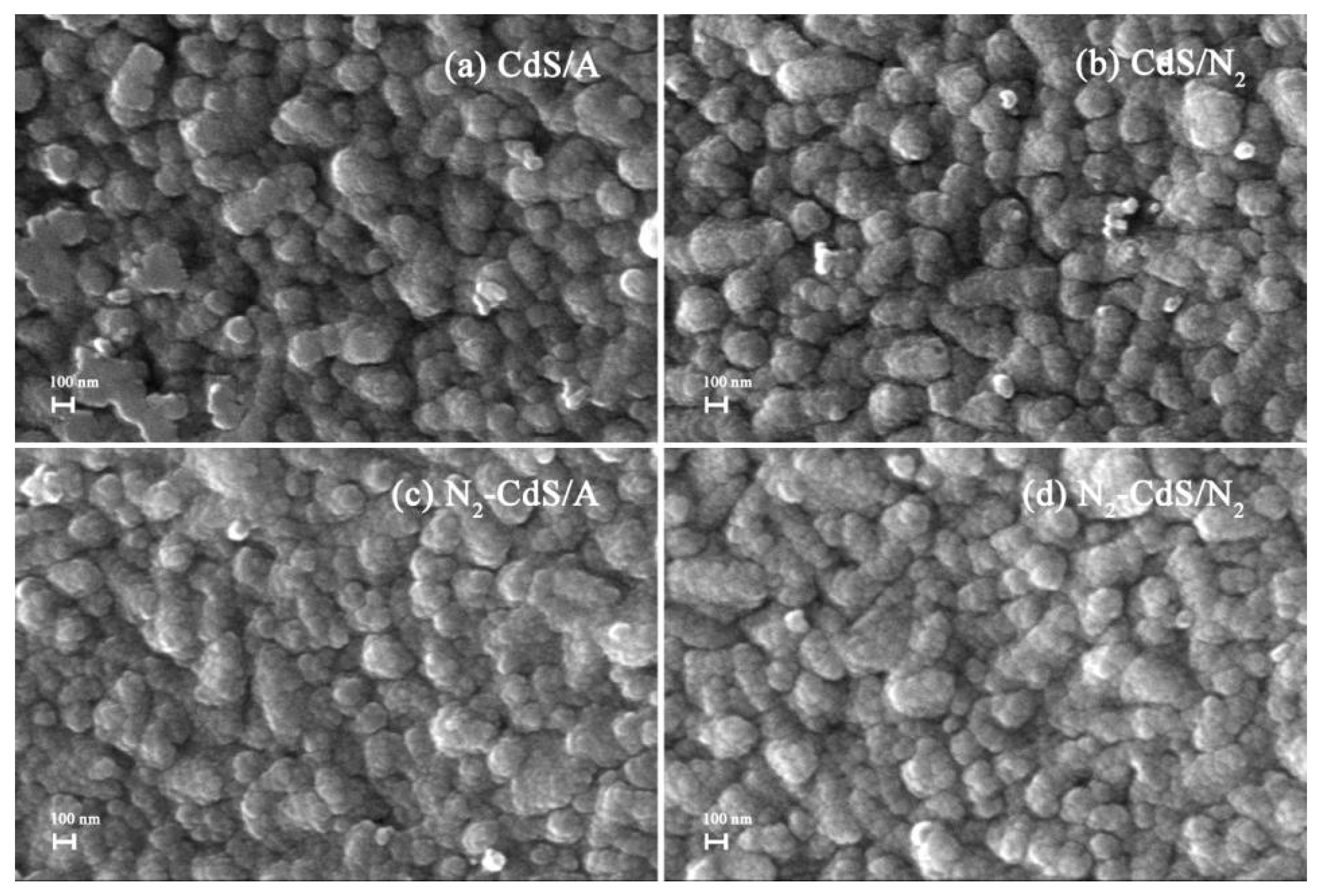
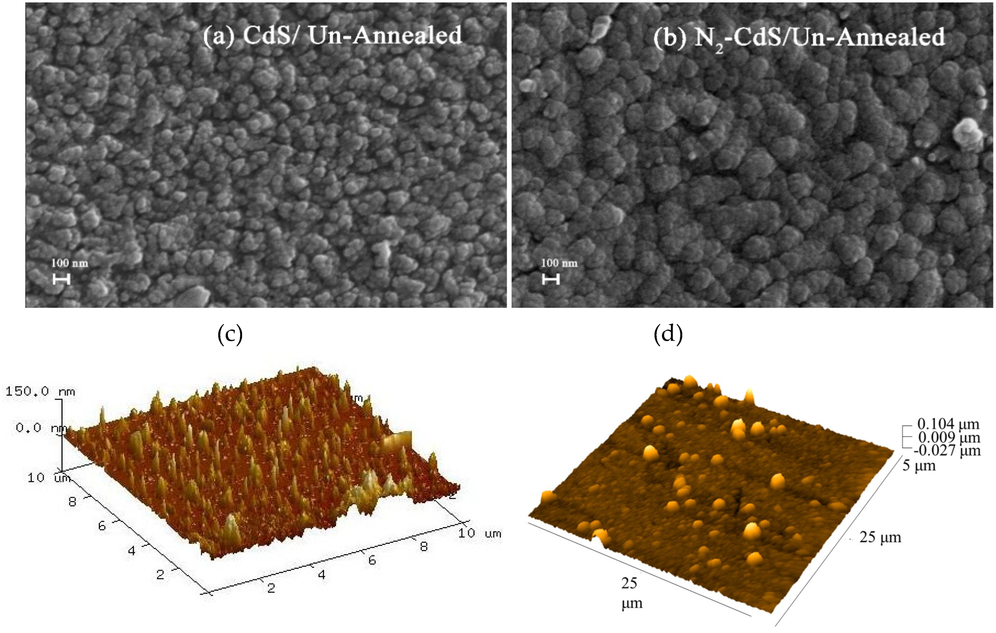
3.3. Morphological Analysis

Figure 7a–d show the SEM images of CdS/A, CdS/N2, N2-CdS/A, and N2-CdS/N2, respectively. All the films were annealed at 300 °C. The figures suggest that the surfaces of the grown CdS films contain spherical topographies with diverse sizes. According to the results, it is possible to state that N2 purged films (N2-CdS/A and N2-CdS/N2) show smooth morphology compared to the non-purged CdS/A and CdS/N2 (Table 2). It is also evident from the SEM images that both N2-CdS/A and N2-CdS/N2 have better interconnectivity compared to CdS/A and CdS/N2. Therefore, better electrical properties obtained for N2 purged samples compared to the rest of the samples is understandable.
Furthermore, as seen in SEM images in Figure 7a,b, the film surface of films CdS/A and CdS/N2 have rougher topography compared to N2-CdS/A and N2-CdS/N2 (Table 2). Rough surfaces tend to scatter more light and hence give way to low transmittance [37]. Hence, the higher transmittance recorded for N2 purged films, as seen in Figure 1, could potentially be due to this effect besides the better crystallinity.
Figure 8a,b show the SEM images obtained for un-purged/un-annealed and N2 purged/un-annealed CdS films, respectively. It is evident that N2 purging has improved the size of the clusters. The improvement of the cluster size is due to the merging of small clusters which are about 25 nm in size. This can be the reason for the observed relative smooth surface in the N2 purged samples as seen in Figure 8c,d.
At a deposition temperature of 80 °C, CdS is expected to be deposited through the cluster-by-cluster process. This occurs via agglomeration of colloidal Cd(OH)2 particles pre-formed in solution through homogeneous nucleation as mentioned in Equations (5)–(8) above. When a CdS film is deposited by the cluster-by-cluster method, one possible shortcoming is the adherence of loosely bound large Cd(OH)2 particles onto the substrate. But with the introduction of N2 purging into the solution bath, adherence of loosely bound large Cd(OH)2 can be minimized, potentially due to solution agitation. According to Figure 4, both the N2 purged films (irrespective of whether air annealed or N2 annealed) show better Isc values compared to the rest. This result may well be because of the better interconnectivity between the CdS clusters as a result of N2 purging.

3.4. Compositional Analysis

Compositional analysis of the films CdS/A, CdS/N2, N2-CdS/A, and N2-CdS/N2 were conducted using EDX analysis. All the films were annealed at 300 °C. The S:Cd ratio was determined using the EDX spectra, and the results obtained from the analysis are given in Table 2. According to the results, the highest S:Cd ratio was observed for the film CdS/A, while the lowest ratio was seen for N2-CdS/N2.
A lower S:Cd ratio can lead to a decrement in the resistivity of the films and hence an improved electrical property [38]. Therefore, the result also suggests that the better electrical properties of N2-CdS/N2 can also be due to apparent S deficiency.
In the literature, the deficiency in S compared to Cd has been explained as a result of the existence of oxygen in the sub lattice of sulfur due to the transformation of Cd(OH)2 in the as-grown films as explained in Equations (2)–(5) and Equations (2)–(7) [39]. Also, it is known that the dimensions of oxygen atoms are smaller than the dimensions of sulfur [40]. Hence, the variation in the crystallite size can be resulted from the variation in the S:Cd ratio. Formation of O2 can be one of the reasons for the increment in the S:Cd ratio which in turn potentially affect the residual stress of the film. Furthermore, annealing some Cd(OH)2 (Equation (11)) precipitates in the film may convert to CdO, releasing water vapor that triggers additional oxidation. Even a small percentage of oxidation can lead to a significant decrease in the optical energy gap, which represents the minimum energy required for band-to-band transition. Consequently, in a mixture of CdS and CdO, the measured energy gap corresponds to that of CdO during transmission measurements [31].

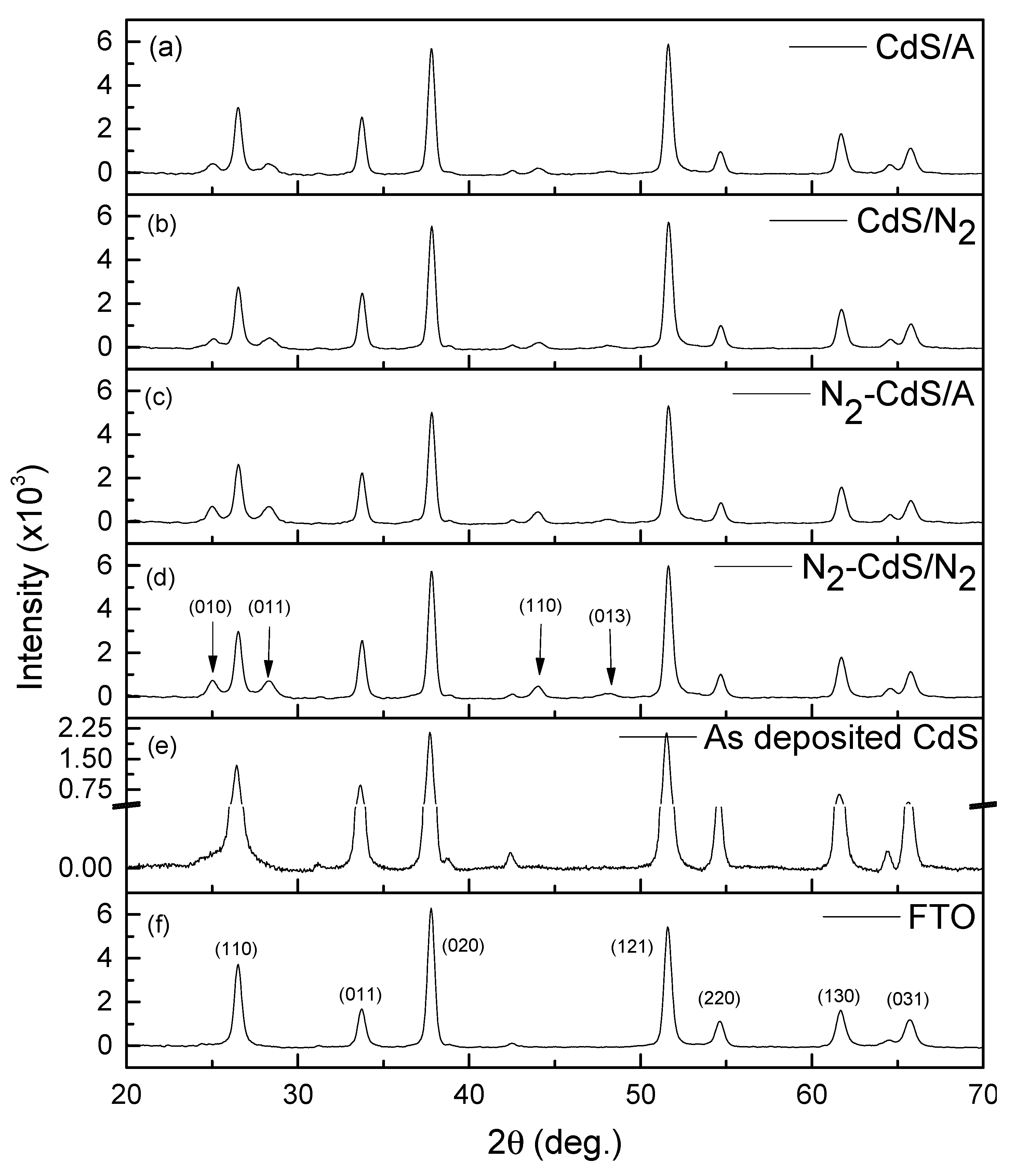
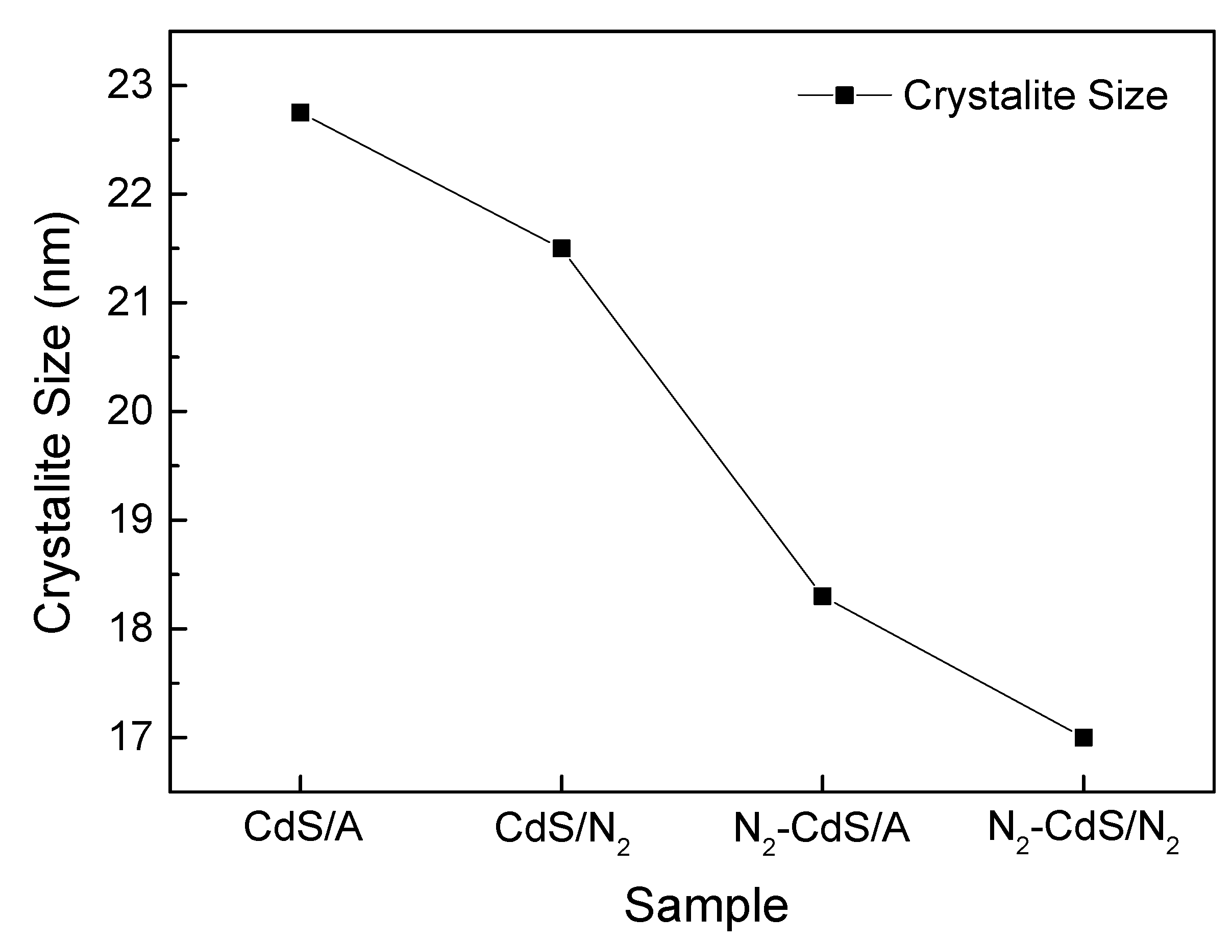
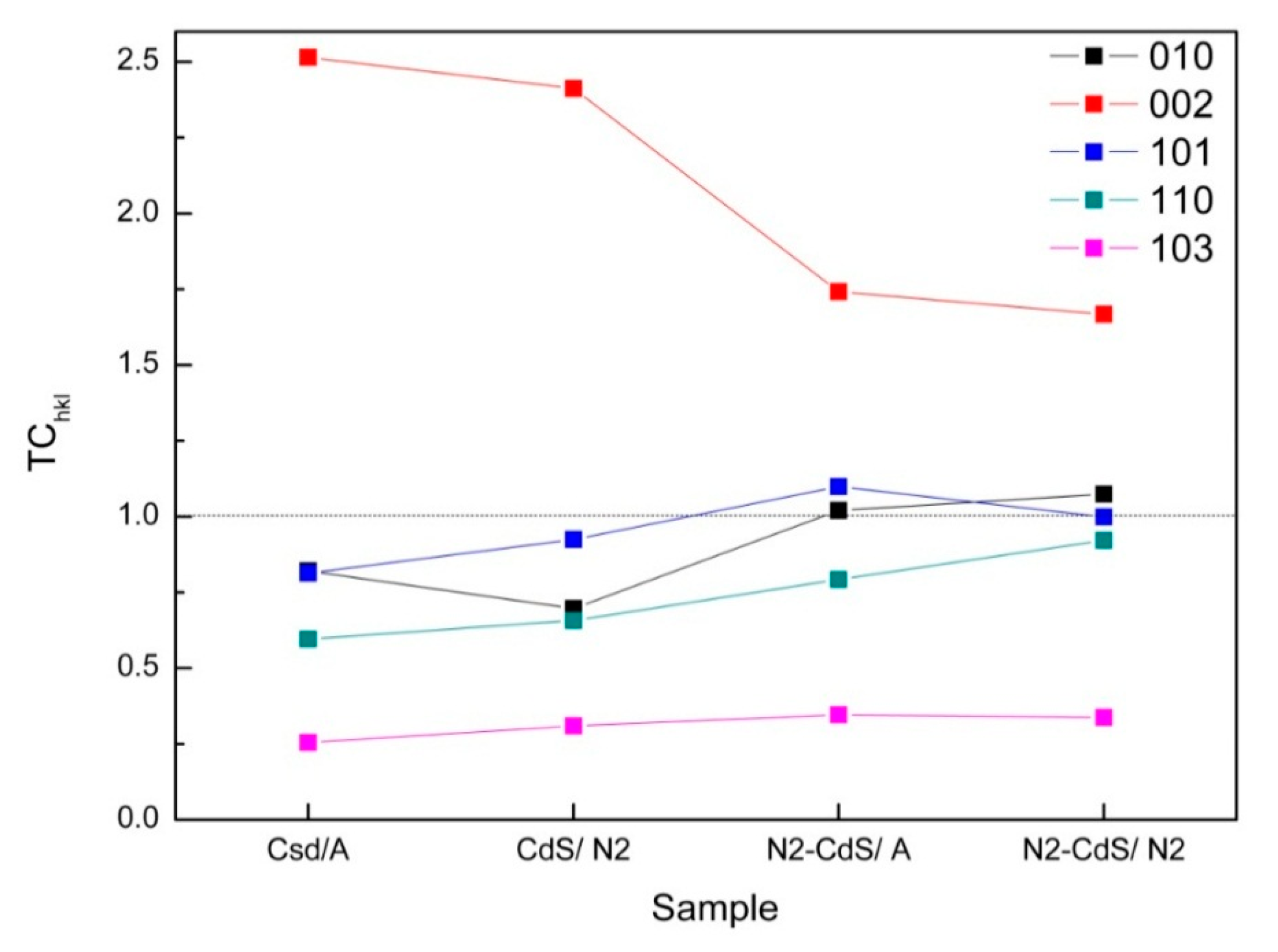
3.5. Structural Analysis

It is a known factor that the optical, as well as the electrical, behavior of thin films can be affected by the structural properties. The obtained results for all four types of films annealed at 300 °C for 1 h along with GIXRD results for bare FTO substrate is shown in Figure 9. The diffraction peaks at 25.00°, 26.52°, 28.28°, 43.94°, and 48.01° in Figure 9a–e were identified to be corresponding to hexagonal (010), (002), (011), (110), and (013) planes of CdS (JCPDS 98-009-5006). The rest of the peaks appearing are from the FTO substrate on which the films were deposited on. According to the result, irrespective of the method of annealing, there is no evidence to support the formation of oxides in the grown films.
The crystallite size of the grown films can be investigated using Williamson Hall (WH) plots by [41,42].
β hkl cos θ = K λ D + 4 ε sin θ
where λ is the wavelength of X–rays used for the measurement, K is the shape factor, ε is the macrostrain, D is the crystallite size, and θ is the diffraction angle. The intercept of the linear plot between β hkl cos θ and sin θ can be used to calculate the crystallite size of the grown films. Calculated crystallite sizes are shown in Figure 10. According to the figure, N2 purging seems to adversely affect the crystallite size. Nevertheless, the reduction in crystallite size within CdS thin films demonstrates a notable augmentation in both open-circuit voltage (Voc) and short-circuit current (Isc) characteristics, as illustrated in Figure 6, attributed to the corresponding increase in surface area [43,44].
The preferential crystallite orientation in the films was investigated by calculating the texture coefficient (TChkl) of the samples. The TChkl was calculated for all the grown CdS film using Equation (13) [45,46].
T C h k l   =   I ( h k l ) I 0 ( h k l ) 1 n i = 1 n I ( h k l ) I o ( h k l )
where n is the number of X-ray diffraction peaks, I0(hkl) is the standard intensity of the plane (hkl) taken from the JCPDS data (JCPDS 98-009-5006), and I(hkl) is the measured relative intensity of a plane (hkl). The calculated TChkl for samples CdS/A, CdS/N2, N2-CdS/A, and N2-CdS/N2 are shown in Figure 11. The figure demonstrates that (002) appears to be the greatest preferred orientation for all the samples investigated.
The obtained crystallographic data do not support a significant change in the crystal structure of the grown films or the existence of oxides. Hence, the improvement in the electrical and optical properties seen due to N2 purging and annealing is more likely a result of the improvement in the surface morphology, composition, and roughness of the grown films as described earlier.

4. Conclusions

Two different sets of CdS thin films were successfully grown on FTO glass substrates under N2 purged and un-purged conditions. Later, both sets of films were annealed in two different annealing environments: N2 annealing and air annealing in the temperature range of 100–500 °C. The films that underwent both N2-purging and N2-annealing showed a 5% improvement in optical transmittance compared to the conventional CdS thin films. The Isc and Voc values of all the grown films in the PEC cell of FTO/CdS/0.1 M Na2S2O3/Pt were found to be increased irrespective of the deposition method before it decreased beyond the annealing temperature of 300 °C. The films that underwent both N2-purging and N2-annealing showed the highest ISC and VOC in the PEC cell of FTO/CdS/0.1 M Na2S2O3/Pt under an annealing temperature of 300 °C. The ISC, VOC, and VFB values of N2-purging and N2-annealing films showed 37.5%, 27%, and 24% improvements with respect to conventional CdS films.
The better electrical properties observed in N2 purged samples could be resulted from the well-packed nature and better interconnectivity, which was evident from the SEM images. Additionally, the higher S:Cd ratio in the N2-purged and N2-annealed films compared to the rest can also be a possible reason for the improved electrical properties of the proposed novel CdS deposition method. The study suggests that N2 purged and N2 annealed CBD-CdS films yield better optical as well as electrical properties compared to conventional deposition methods.

Author Contributions

Conceptualization, G.W.C.K. and B.S.D.; methodology, G.K.L.S. and G.R.K.K.G.R.K.; validation, B.S.D. and G.W.C.K.; formal analysis, G.K.L.S., G.R.K.K.G.R.K. and G.W.C.K.; investigation G.K.L.S. and G.R.K.K.G.R.K.; resources, B.S.D.; data curation, G.K.L.S., G.R.K.K.G.R.K. and G.W.C.K.; writing—original draft preparation, G.K.L.S., G.R.K.K.G.R.K. and G.W.C.K.; writing—review and editing, G.W.C.K. and B.S.D.; visualization, G.W.C.K.; supervision, G.W.C.K. and B.S.D.; project administration, B.S.D.; funding acquisition, B.S.D. All authors have read and agreed to the published version of the manuscript.

Funding

This project was financially supported by the Solar Edu-Training project of the State Ministry of Skills Development, Vocational Education, Research and Innovation, Sri Lanka.

Data Availability Statement

The data presented in this study are available on request from the corresponding author.

Acknowledgments

A portion of the research was conducted at the Department of Physics and Electronics, Faculty of Science, University of Kelaniya, Sri Lanka. This paper is dedicated to the memory of our collaborator and co-author, Buddhika S. Dassanayake, who tragically passed away on 25 December 2023.

Conflicts of Interest

The authors declare no conflicts of interest.

References

  1. Oliva, A. Formation of the Band Gap Energy on CdS Thin Films Growth by Two Different Techniques. Thin Solid Films 2001, 391, 28–35. [Google Scholar] [CrossRef]
  2. Zhai, T.; Fang, X.; Li, L.; Bando, Y.; Golberg, D. One-Dimensional CdS Nanostructures: Synthesis, Properties, and Applications. Nanoscale 2010, 2, 168–187. [Google Scholar] [CrossRef]
  3. Deshmukh, L.P.; Palwe, A.B.; Sawant, V.S. Deposition and Characterisations of CdS and CdS: As Thin Films. Sol. Energy Mater. 1990, 20, 341–348. [Google Scholar] [CrossRef]
  4. Kumar, S.; Kumar, S.; Sharma, P.; Sharma, V.; Katyal, S.C. CdS Nanofilms: Effect of Film Thickness on Morphology and Optical Band Gap. J. Appl. Phys. 2012, 112, 123512. [Google Scholar] [CrossRef]
  5. Metin, H.; Ari, M.; Erat, S.; Durmuş, S.; Bozoklu, M.; Braun, A. The Effect of Annealing Temperature on the Structural, Optical, and Electrical Properties of CdS Films. J. Mater. Res. 2010, 25, 189–196. [Google Scholar] [CrossRef]
  6. Zhou, L.M.; Hu, X.F.; Wu, S.M. Effects of Ph Value on Performance of CdS Films with Chemical Bath Deposition. Adv. Mater. Res. 2012, 557–559, 1941–1944. [Google Scholar] [CrossRef]
  7. Kumarage, W.G.C.; Wijesundara, L.B.D.R.P.; Seneviratne, V.A.; Jayalath, C.P.; Dassanayake, B.S. Influence of Bath Temperature on CBD-CdS Thin Films. Procedia Eng. 2016, 139, 64–68. [Google Scholar] [CrossRef]
  8. Wenyi, L.; Xun, C.; Qiulong, C.; Zhibin, Z. Influence of Growth Process on the Structural, Optical and Electrical Properties of CBD-CdS Films. Mater. Lett. 2005, 59, 1–5. [Google Scholar] [CrossRef]
  9. Rondiya, S.; Rokade, A.; Gabhale, B.; Pandharkar, S.; Chaudhari, M.; Date, A.; Chaudhary, M.; Pathan, H.; Jadkar, S. Effect of Bath Temperature on Optical and Morphology Properties of CdS Thin Films Grown by Chemical Bath Deposition. Energy Procedia 2017, 110, 202–209. [Google Scholar] [CrossRef]
  10. Cho, J.Y.; Sinha, S.; Gang, M.G.; Heo, J. Controlled Thickness of a Chemical-Bath-Deposited CdS Buffer Layer for a SNS Thin Film Solar Cell with More than 3% Efficiency. J. Alloys Compd. 2019, 796, 160–166. [Google Scholar] [CrossRef]
  11. Joshi, R.A.; Gupta, M.; Phase, D.M. Annealing Induced Modifications in Physicochemical and Optoelectronic Properties of CdS/CuInGaSe2 Thin Film. Sol. Energy 2019, 177, 1–7. [Google Scholar] [CrossRef]
  12. Shaikh, R.A.; More, S.A.; Bisen, G.G.; Jadkar, S.R.; Sali, J.V.; Ghosh, S.S. Effect of Thermal Annealing and Cooling Rate on CBD Grown CdS Thin Films. J. Mater. Sci. Mater. Electron. 2019, 30, 20354–20359. [Google Scholar] [CrossRef]
  13. Padam, G.K.; Malhotra, G.L.; Rao, S.U. Studies on Solution-Grown Thin Films of ZnxCd1−xS. J. Appl. Phys. 1988, 63, 770–774. [Google Scholar] [CrossRef]
  14. Jun-feng, H.; Gan-hua, F.; Krishnakumar, V.; Cheng, L.; Jaegermann, W. CdS Annealing Treatments in Various Atmospheres and Effects on Performances of CdTe/CdS Solar Cells. J. Mater. Sci. Mater. Electron. 2013, 24, 2695–2700. [Google Scholar] [CrossRef]
  15. Kumarage, W.G.C.; Wijesundera, R.P.; Kaur, N.; Zappa, D.; Seneviratne, V.A.; Jayalath, C.P.; Dassanayake, B.S. A Comparative Assessment: Chemical Bath Deposited and Electrodeposited CdS Films. Int. J. Electroact. Mater. 2019, 7, 1–6. [Google Scholar]
  16. Adikaram, K.K.; Kumarage, W.G.; Varga, T.; Dassanayake, B.S. Improvement of the Photo-Activity of CdS Thin Films Using TX-100. J. Electron. Mater. 2019, 48, 4424–4431. [Google Scholar] [CrossRef]
  17. Kumarage, W.G.; Wijesundera, R.P.; Seneviratne, V.A.; Jayalath, C.P.; Kaur, N.; Comini, E.; Gunawardhana, N.; Dassanayake, B.S. A Study on CdCl2 Activation of CBD-CdS Films. J. Mater. Sci. Mater. Electron. 2020, 31, 13330–13336. [Google Scholar] [CrossRef]
  18. Kumarage, W.G.C.; Wijesundera, R.P.; Seneviratne, V.A.; Jayalath, C.P.; Kaur, N.; Comini, E.; Dassanayake, B.S. MgCl2 Activation of CdS Films: An Alternative for CdCl2. J. Photochem. Photobiol. A Chem. 2018, 367, 171–177. [Google Scholar] [CrossRef]
  19. Kumarage, W.G.; Wijesundera, R.P.; Seneviratne, V.A.; Jayalath, C.P.; Dassanayake, B.S. A Study on the Enhancement of Opto-Electronic Properties of CdS Thin Films: Seed-Assisted Fabrication. Semicond. Sci. Technol. 2017, 32, 045014. [Google Scholar] [CrossRef]
  20. Najm, A.S.; Naeem, H.S.; Alwarid, D.A.R.M.; Aljuhani, A.; Hasbullah, S.A.; Hasan, H.A.; Sopian, K.; Bais, B.; Al-Iessa, H.J.; Majdi, H.S.; et al. Mechanism of Chemical Bath Deposition of CdS Thin Films: Influence of Sulphur Precursor Concentration on Microstructural and Optoelectronic Characterizations. Coatings 2022, 12, 1400. [Google Scholar] [CrossRef]
  21. Hodes, G. Chemical Solution Deposition of Semiconductor Films; Dekker: New York, NY, USA, 2002; pp. 1–45. [Google Scholar]
  22. Najm, A.S.; Naeem, H.S.; Majdi, H.S.; Hasbullah, S.A.; Hasan, H.A.; Sopian, K.; Bais, B.; Al-Iessa, H.J.; Dhahad, H.A.; Ali, J.M.; et al. An In-Depth Analysis of Nucleation and Growth Mechanism of CdS Thin Film Synthesized by Chemical Bath Deposition (CBD) Technique. Sci. Rep. 2022, 12, 15295. [Google Scholar] [CrossRef]
  23. Kumarasinghe, R.K.; Kumarage, W.G.; Wijesundera, R.P.; Kaur, N.; Comini, E.; Dassanayake, B.S. A Comparative Study on CdS Film Formation under Variable and Steady Bath-Temperature Conditions. Semiconductors 2020, 54, 838–843. [Google Scholar] [CrossRef]
  24. Kumarage, W.G.; Wijesundera, R.P.; Seneviratne, V.A.; Jayalath, C.P.; Dassanayake, B.S. Tunable Optoelectronic Properties of CBD-CdS Thin Films via Bath Temperature Alterations. J. Phys. D Appl. Phys. 2016, 49, 095109. [Google Scholar] [CrossRef]
  25. Maticiuc, N.; Kukk, M.; Spalatu, N.; Potlog, T.; Krunks, M.; Valdna, V.; Hiie, J. Comparative Study of CdS Films Annealed in Neutral, Oxidizing and Reducing Atmospheres. Energy Procedia 2014, 44, 77–84. [Google Scholar] [CrossRef]
  26. Das, C.; Begum, J.; Begum, T.; Choudhury, S. Effect of Thickness on the Optical Properties of GaAs Thin Films. J. Bangladesh Acad. Sci. 2013, 37, 83–91. [Google Scholar] [CrossRef]
  27. Moualkia, H.; Rekhila, G.; Izerrouken, M.; Mahdjoub, A.; Trari, M. Influence of the Film Thickness on the Photovoltaic Properties of Chemically Deposited CdS Thin Films: Application to the Photodegradation of Orange II. Mater. Sci. Semicond. Process. 2014, 21, 186–193. [Google Scholar] [CrossRef]
  28. Rangel-Cárdenas, J.; Sobral, H. Optical Absorption Enhancement in CdTe Thin Films by Microstructuration of the Silicon Substrate. Materials 2017, 10, 607. [Google Scholar] [CrossRef]
  29. Moualkia, H.; Hariech, S.; Aida, M.S. Structural and Optical Properties of CdS Thin Films Grown by Chemical Bath Deposition. Thin Solid Film. 2009, 518, 1259–1262. [Google Scholar] [CrossRef]
  30. Metin, H.; Esen, R. Annealing Studies on CBD Grown CdS Thin Films. J. Cryst. Growth 2003, 258, 141–148. [Google Scholar] [CrossRef]
  31. Metin, H.; Esen, R. Annealing Effects on Optical and Crystallographic Properties of CBD Grown CdS Films. Semicond. Sci. Technol. 2003, 18, 647–654. [Google Scholar] [CrossRef]
  32. Ichimura, M.; Goto, F.; Arai, E. Structural and Optical Characterization of CdS Films Grown by Photochemical Deposition. J. Appl. Phys. 1999, 85, 7411–7417. [Google Scholar] [CrossRef]
  33. Moualkia, H.; Hariech, S.; Aida, M.S.; Attaf, N.; Laifa, E.L. Growth and Physical Properties of CdS Thin Films Prepared by Chemical Bath Deposition. J. Phys. D Appl. Phys. 2009, 42, 135404. [Google Scholar] [CrossRef]
  34. Hodes, G.; Albu-Yaron, A.; Decker, F.; Motisuke, P. Three-Dimensional Quantum-Size Effect in Chemically Deposited Cadmium Selenide Films. Phys. Rev. B 1987, 36, 4215–4221. [Google Scholar] [CrossRef] [PubMed]
  35. Pathinettam Padiyan, D.; Marikani, A.; Murali, K.R. Influence of Thickness and Substrate Temperature on Electrical and Photoelectrical Properties of Vacuum-Deposited CdSe Thin Films. Mater. Chem. Phys. 2003, 78, 51–58. [Google Scholar] [CrossRef]
  36. Morrison, S.R. Electrochemistry at Semiconductor and Oxidized Metal Electrodes; Plenum Press: New York, NY, USA, 1980; pp. 119–149. [Google Scholar]
  37. Liu, F.; Lai, Y.; Liu, J.; Wang, B.; Kuang, S.; Zhang, Z.; Li, J.; Liu, Y. Characterization of Chemical Bath Deposited CdS Thin Films at Different Deposition Temperature. J. Alloys Compd. 2010, 493, 305–308. [Google Scholar] [CrossRef]
  38. Aguilar-Hernández, J.; Sastre-Hernández, J.; Ximello-Quiebras, N.; Mendoza-Pérez, R.; Vigil-Galán, O.; Contreras-Puente, G.; Cárdenas-García, M. Photoluminescence Studies on CdS-CBD Films Grown by Using Different S/CD Ratios. Thin Solid Film. 2006, 511–512, 143–146. [Google Scholar] [CrossRef]
  39. Maticiuc, N.; Hiie, J.; Potlog, T.; Valdna, V.; Gavrilov, A. Influence of Annealing in H2 Atmosphere on the Electrical Properties of Thin Film CdS. MRS Proc. 2011, 1324, mrss11-1324-d14-05. [Google Scholar] [CrossRef]
  40. Maticiuc, N.; Hiie, J.; Mikli, V.; Potlog, T.; Valdna, V. Structural and Optical Properties of Cadmium Sulfide Thin Films Modified by Hydrogen Annealing. Mater. Sci. Semicond. Process. 2014, 26, 169–174. [Google Scholar] [CrossRef]
  41. Mote, V.; Purushotham, Y.; Dole, B. Williamson-Hall Analysis in Estimation of Lattice Strain in Nanometer-Sized ZnO Particles. J. Theor. Appl. Phys. 2012, 6, 6. [Google Scholar] [CrossRef]
  42. Kumarasinghe, P.K.; Dissanayake, A.; Pemasiri, B.M.; Dassanayake, B.S. Variation of Optical, Structural, Electrical and Compositional Properties of Thermally Evaporated CdTe Thin Films Due to Substrate Temperature. J. Mater. Sci. Mater. Electron. 2016, 28, 276–283. [Google Scholar] [CrossRef]
  43. Rahman, M.F.; Hossain, J.; Ismail, A.B. Structural, Surface Morphological and Optical Properties and Their Correlation with the Thickness of Spin Coated Superior Quality CdS Thin Film Synthesized Using a Novel Chemical Route. SN Appl. Sci. 2020, 2, 1956. [Google Scholar] [CrossRef]
  44. Ma, X.; Zhu, Y.; Lu, L.; Liang, C.; Chen, Q.; Liao, Y. Particle Size and Temperature Effects on Surface Thermodynamic Functions and Particle Size Effects on Prescribed Thermodynamic Functions for Cadmium Sulfide Nanospheres. Mater. Chem. Phys. 2021, 260, 124050. [Google Scholar] [CrossRef]
  45. Du, S.; Li, Y. Effect of Annealing on Microstructure and Mechanical Properties of Magnetron Sputtered CU Thin Films. Adv. Mater. Sci. Eng. 2015, 2015, 969580. [Google Scholar] [CrossRef]
  46. Bilgin, V.; Kose, S.; Atay, F.; Akyuz, I. The Effect of SN Concentration on Some Physical Properties of Zinc Oxide Films Prepared by Ultrasonic Spray Pyrolysis. J. Mater. Sci. 2005, 40, 1909–1915. [Google Scholar] [CrossRef]
Figure 1. Optical transmittance of the CBD-CdS annealed from 100 to 500 °C; (a) CdS/A; (b) CdS/N2; (c) N2-CdS/A; (d) N2-CdS/N2.
Electronicmat 05 00003 g001
Figure 2. Variation of Eg of the four different types of samples with respect to annealing temperature.
Electronicmat 05 00003 g002
Figure 3. The variation in VOC value of the four different types of CdS films at different annealing temperatures.
Electronicmat 05 00003 g003
Figure 4. The variation in ISC value of the four different types of CdS films deposited at different annealing temperatures.
Electronicmat 05 00003 g004
Figure 5. The variation in ISC × VOC value of the four different types of CdS films deposited at different annealing temperatures.
Electronicmat 05 00003 g005
Figure 6. The variation in VFB value of the four different types of CdS films deposited at different annealing temperatures.
Electronicmat 05 00003 g006
Figure 7. SEM images of the CdS films; (a) CdS/A; (b) CdS/N2; (c) N2-CdS/A; (d) N2-CdS/N2 annealed at 300 °C for 1 h.
Electronicmat 05 00003 g007
Figure 8. SEM and AFM images of the CdS films; (a,c) unannealed and unpurged CdS; (b,d) N2 purged and un-annealed CdS.
Electronicmat 05 00003 g008
Figure 9. X-ray diffractograms of the (a) CdS/A; (b) CdS/N2; (c) N2-CdS/A; (d) N2-CdS/N2 thin films annealed at 300 °C for 1 h; (e) as-deposited CdS; (f) bare FTO.
Electronicmat 05 00003 g009
Figure 10. Crystal size of the CdS/A, CdS/N2, N2-CdS/A, and N2-CdS/N2.
Electronicmat 05 00003 g010
Figure 11. Texture coefficient of CBD-CdS/A, CdS/N2, N2-CdS/A, and N2-CdS/N2 films.
Electronicmat 05 00003 g011
Table 1. Details of the four different types of grown films.
PurgingAnnealing EnvironmentCode
NoAirCdS/A
NoN2CdS/N2
N2AirN2-CdS/A
N2N2N2-CdS/N2
Table 2. S:Cd ratio and roughness for CdS/A, CdS/N2, N2-CdS/A, and N2-CdS/N2.
SampleS:CdRoughness (nm)
CdS/A0.8625.6
CdS/N20.8119.7
N2-CdS/A0.8011.6
N2-CdS/N20.7111.0
Disclaimer/Publisher’s Note: The statements, opinions and data contained in all publications are solely those of the individual author(s) and contributor(s) and not of MDPI and/or the editor(s). MDPI and/or the editor(s) disclaim responsibility for any injury to people or property resulting from any ideas, methods, instructions or products referred to in the content.

