Article

Insulator Metal Transition-Based Selector in Crossbar Memory Arrays

Department of Electron Devices, Faculty of Electrical Engineering and Informatics, Budapest University of Technology and Economics, H-1111 Budapest, Hungary
*
Author to whom correspondence should be addressed.
Electron. Mater. 2024, 5(1), 17-29; https://doi.org/10.3390/electronicmat5010002
Submission received: 1 January 2024 / Revised: 23 January 2024 / Accepted: 21 February 2024 / Published: 23 February 2024

Abstract

:
This article investigates resistive random access memory (ReRAM) crossbar memory arrays, which is a notable development in non-volatile memory technology. We highlight ReRAM’s competitive edge over NAND, NOR Flash, and phase-change memory (PCM), particularly in terms of endurance, speed, and energy efficiency. This paper focuses on the architecture of crossbar arrays, where memristive devices are positioned at intersecting metal wires. We emphasize the unique resistive switching mechanisms of memristors and the challenges of sneak path currents and delve into the roles and configurations of selectors, particularly focusing on the one-selector one-resistor (1S1R) architecture with an insulator–metal transition (IMT) based selector. We use SPICE simulations based on defined models to examine a 3 × 3 1S1R ReRAM array with vanadium dioxide selectors and titanium dioxide film memristors, assessing the impact of ambient temperature and critical IMT temperatures on array performance. We highlight the operational regions of low resistive state (LRS) and high resistive state (HRS), providing insights into the electrical behavior of these components under various conditions. Lastly, we demonstrate the impact of selector presence on sneak path currents. This research contributes to the overall understanding of ReRAM crossbar arrays integrated with IMT material-based selectors.

1. Introduction

Resistive random access memory (ReRAM) integrated with crossbar memory arrays is a transformative advancement in non-volatile memory (NVM) technology. Compared to NAND Flash, which dominates the market in terms of storage density and is commonly found in solid-state drives (SSDs) and memory cards [1], ReRAM has strong potential to compete in terms of high storage density and faster WRITE speeds, although it is still in the developmental stage and has not achieved the same level of market penetration. NAND Flash, however, does have a substantial lead in terms of cost-effectiveness, owing to its maturity and mass production, even though it falls behind in terms of endurance with ReRAM capable of surpassing 106 program/erase cycles compared to NAND’s 10,000 to 100,000 [2]. On the other hand, NOR Flash, another popular NVM technology known for its random access capabilities and suitability for code storage in embedded applications, also offers high durability and fast WRITE speeds but at a higher cost per bit and slower speed than ReRAM [3]. When placed side by side with phase-change memory (PCM), ReRAM finds a closer competitor, with both technologies showcasing dynamic random-access memory (DRAM) like speeds, good endurance, and excellent scalability for future technology nodes [4]. However, ReRAM outperforms PCM in terms of energy efficiency, especially during WRITE operations, even though PCM is currently more mature in market adoption.

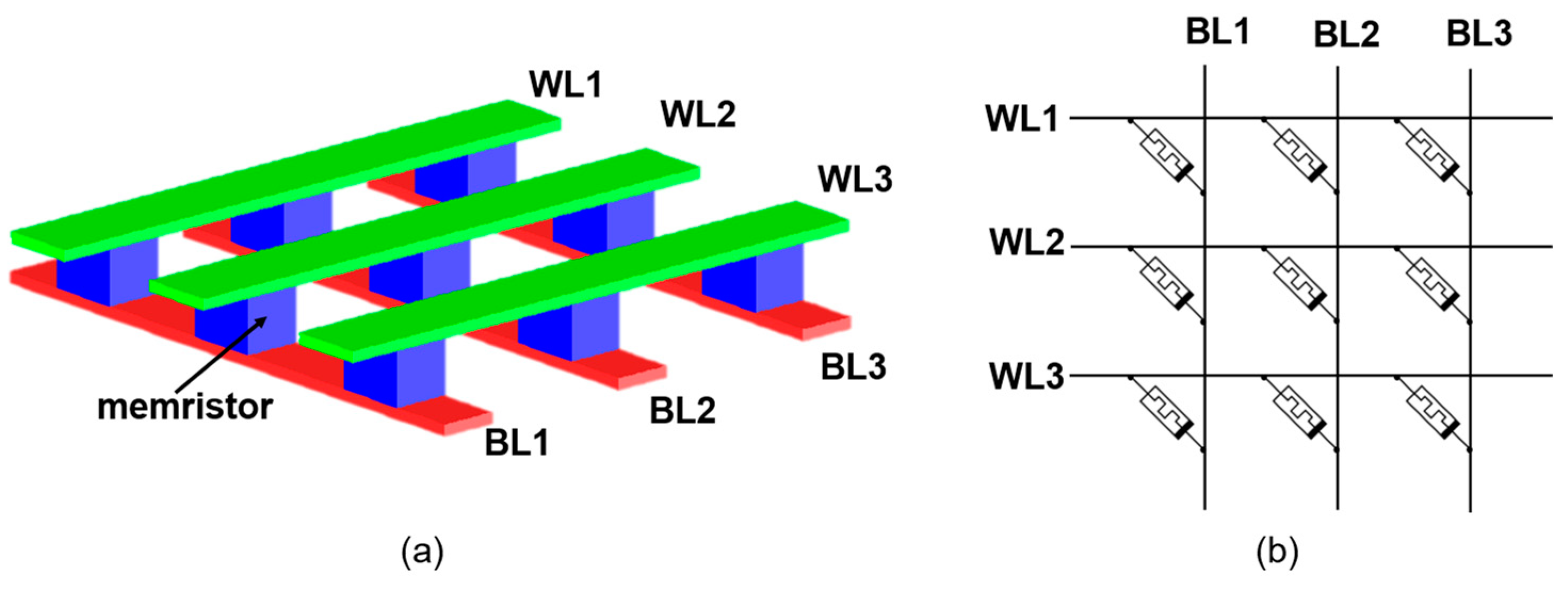
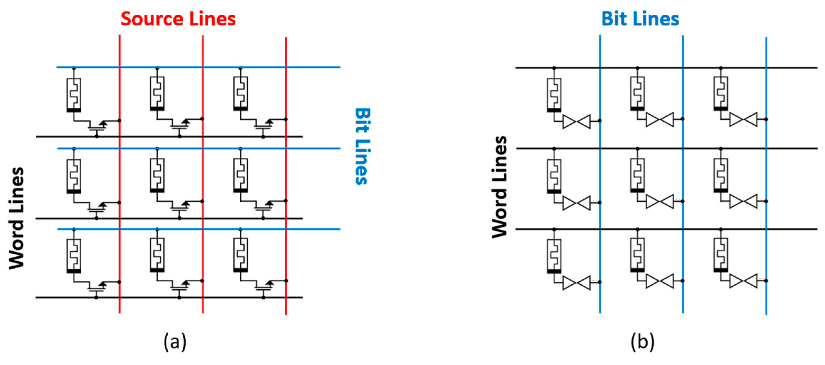
1.1. Crossbar Memory Arrays

The architecture of crossbar memory arrays consists of a two-dimensional matrix of orthogonally intersecting metal wires with memristive devices situated at each intersection, as shown in Figure 1. In most cases, these memristive devices are fabricated from transition metal oxides such as TiO2 or HfO2, which are foundational to ReRAM technology and utilize nanoionic properties to modulate resistance in response to applied electrical biases [5]. The memristor, recognized as the fourth fundamental circuit element, exhibits a unique property where its resistance depends on the history of the voltage applied and the charge that has passed through it [6]. When integrated into crossbar memory arrays, memristor locations at the intersections of perpendicular nanowires enable a non-volatile resistance-switching mechanism.
The architecture of ReRAM crossbar arrays holds potential for implementation in 3D-stacked memories as well, promising unparalleled memory density [7]. This capability is crucial for applications requiring substantial data storage in compact spaces. Regarding energy efficiency, ReRAM’s resistive switching mechanism requires less energy than charge-based memory technologies, such as DRAM or Flash, making it suitable for energy-limited applications. Additionally, the crossbar design minimizes the need for access transistors, substantially reducing the footprint of each memory cell and enhancing the array’s storage density, especially since their two-terminal structure simplifies the integration process, supporting scalability down to nanometer-scale dimensions.

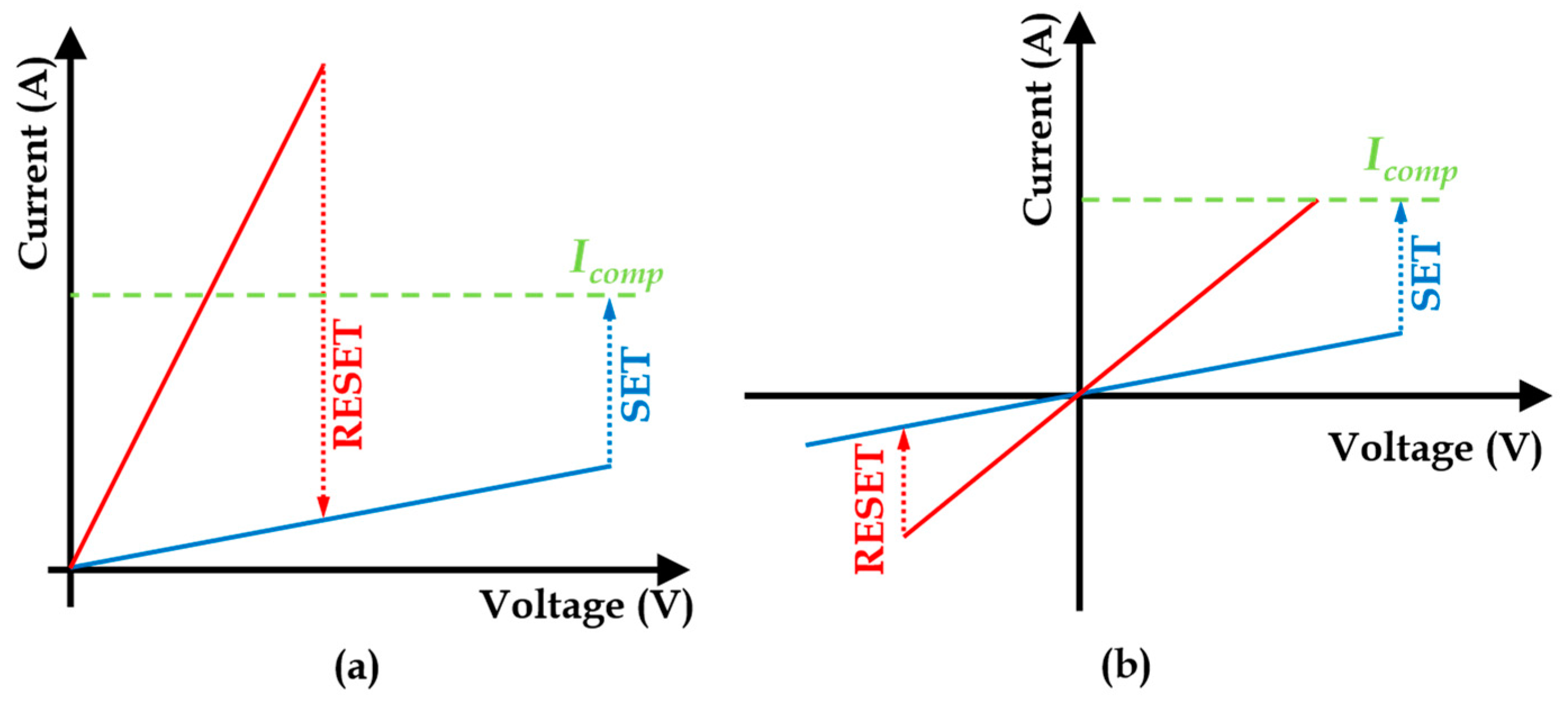
1.2. WRITE and READ Operations
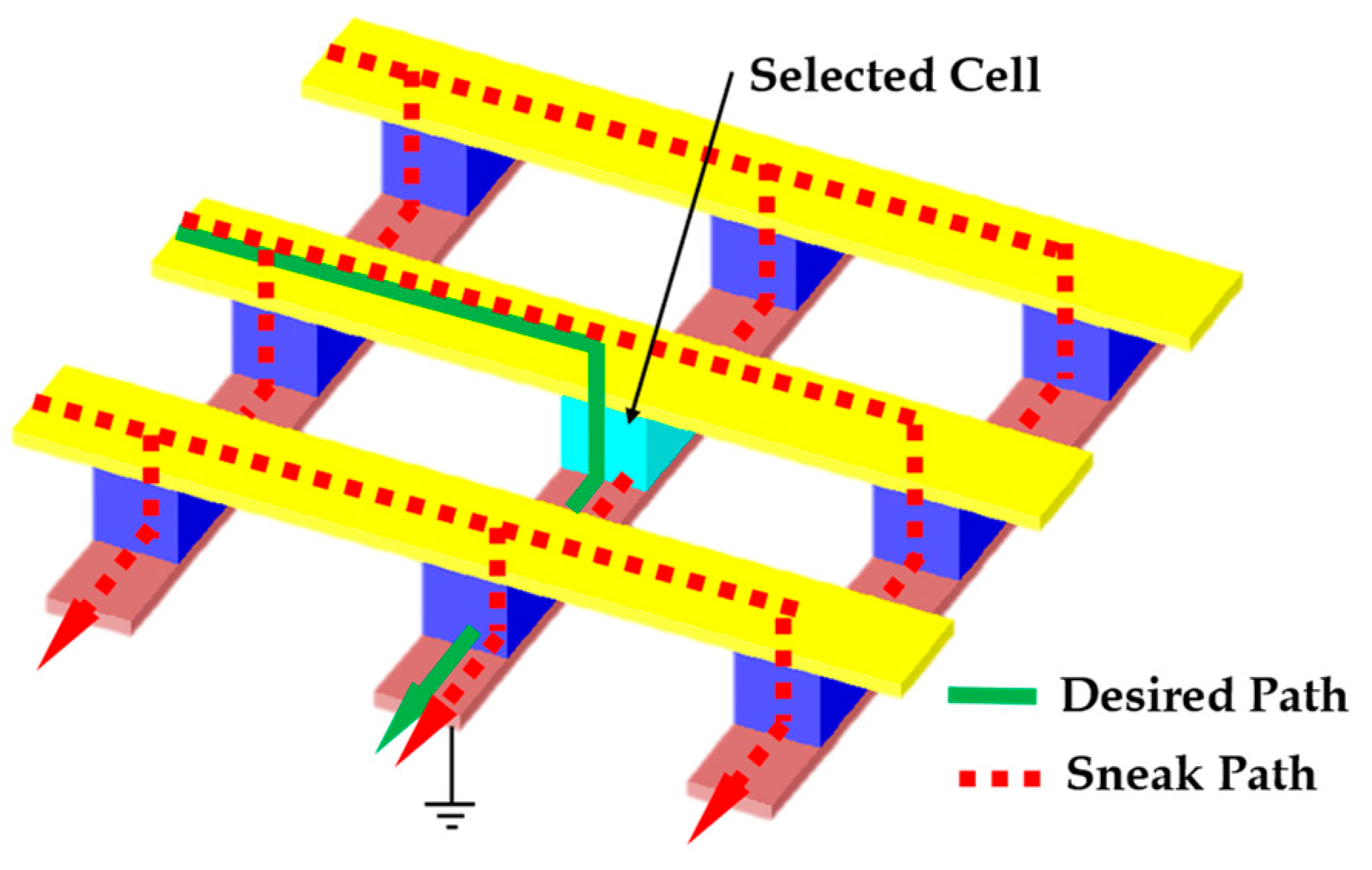
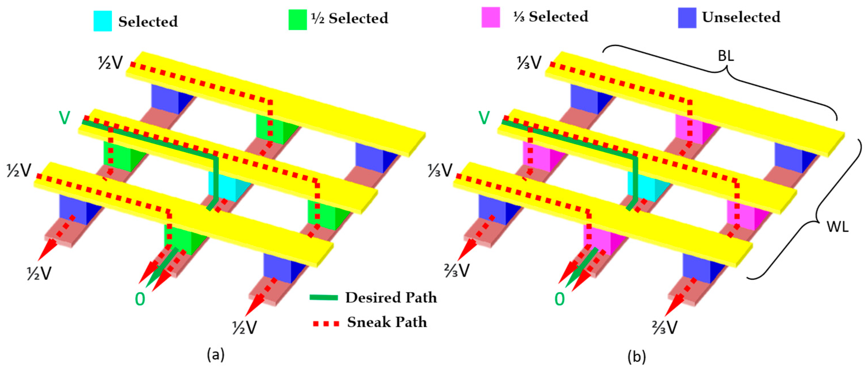
ReRAM’s operation is based on the WRITE and READ operations. WRITE operations require “SET” and “RESET” processes, initiated by applying positive or negative voltage biases in the case of bipolar memristors. In the case of unipolar memristors, different levels of the same polarity voltage biasing correspond to “SET” and “RESET” processes, as shown in Figure 2. The SET process induces a low-resistance state (LRS). Conversely, the RESET process restores a high-resistance state (HRS). Additionally, the resistance states are non-volatile, persisting in the absence of power. The READ operation in ReRAM devices requires precision, where a sub-threshold voltage is applied to measure the current flowing through the device, hence determining its resistance state without inducing any resistive switching.

1.3. Challenges

The crossbar memory arrays of ReRAM face the challenge of sneak path currents [8]. This phenomenon occurs when currents unintentionally flow through adjacent unselected cells during a memory operation, resulting from a crossbar array’s inherent architecture where multiple current paths exist simultaneously [9]. The problem is that when attempting to access a specific memory cell within the array, the applied voltage affects not only the targeted cell but also other cells along the same row and column, potentially leading to incorrect readout values and interference during programming operations. The severity of this issue escalates with the scaling of the array size, making it a critical concern for large crossbar memory arrays [10]. An illustration of the sneak path current in the crossbar array is shown in Figure 3.
Addressing this issue necessitates integrating non-linear selector devices that suppress the sneak path currents by providing highly non-linear current-voltage characteristics [11]. These selectors only allow current to flow when a certain threshold is exceeded, ensuring that the unselected cells are not inadvertently conducting during a READ or WRITE operation [12]. The configurations of ReRAM arrays with selectors are discussed in the following section. Another method to address this issue involves the utilization of unique voltage biasing schemes during the array operation, which are designed to minimize the potential impact of sneak path currents [13]. By carefully controlling the voltage applied to the unselected wordlines and bitlines, the influence of these parasitic currents can be substantially reduced [14]. There are typically two types of voltage biasing schemes: the one-half (½) and the one-third (⅓) biasing schemes, as shown in Figure 4. The half-voltage biasing scheme involves applying half the operational voltage to unselected wordlines and bitlines, while selected wordlines receive full voltage and selected bitlines are grounded. For instance, with a 3 V operational voltage, unselected lines are at 1.5 V, selected wordlines at 3 V, and selected bitlines at 0 V. This ensures the selected cell gets the full voltage while unselected cells receive only half, preventing switching. The one-third voltage scheme further improves this by biasing unselected wordlines at 1 V/3 and unselected bitlines at 2 V/3, with unselected cells experiencing V/3. This reduces unintended switching and power consumption.
Another approach is developing advanced READ/WRITE algorithms that accommodate sneak path currents [15,16]. Despite these mitigation strategies, managing sneak path currents remains a complex challenge that requires careful consideration in the design and operation of crossbar memory arrays [17].

2. Selectors in ReRAM Arrays

ReRAM crossbar arrays can be categorized based on the arrangement and type of resistive switching elements and the integration of selector devices. Firstly, the one-transistor one-resistor (1T1R) configuration has a transistor in series with each ReRAM cell, creating precise access to individual memory cells and mitigating sneak path currents, although this is at the cost of memory density. On the other hand, the one-selector one-resistor (1S1R) configuration replaces the transistor with a selector device, and in this way, balances performance and form factor, which is common in high-density ReRAM applications.

2.1. 1T1R

This configuration offers excellent control over the cell’s operation, ensuring precise programming and readout. Using a transistor also gives the advantage of integrating the memory array with conventional CMOS circuits to allow more complex and sophisticated memory systems. However, including a transistor in the 1T1R architecture results in a larger cell size than that from the 1S1R configuration, which can limit the achievable storage density. In the 1T1R architecture, as shown in Figure 5a, the transistor serves as an access device, providing the necessary isolation for each memory cell and eliminating the issue of sneak path currents. As there is a transistor, the gate terminal is used to activate the desired resistive element.

2.2. 1S1R

On the other hand, there is the 1S1R architecture, in which each memory cell consists of a resistive switching element in series with a selector device, as shown in Figure 5b. The selector is, in this case, a non-linear device, often realized using diodes [18], ovonic threshold switches [19], mixed ionic-electronic conduction-based devices [20], or insulator–metal transition (IMT) devices [21,22,23,24,25]. In this article, we study the latter realization.

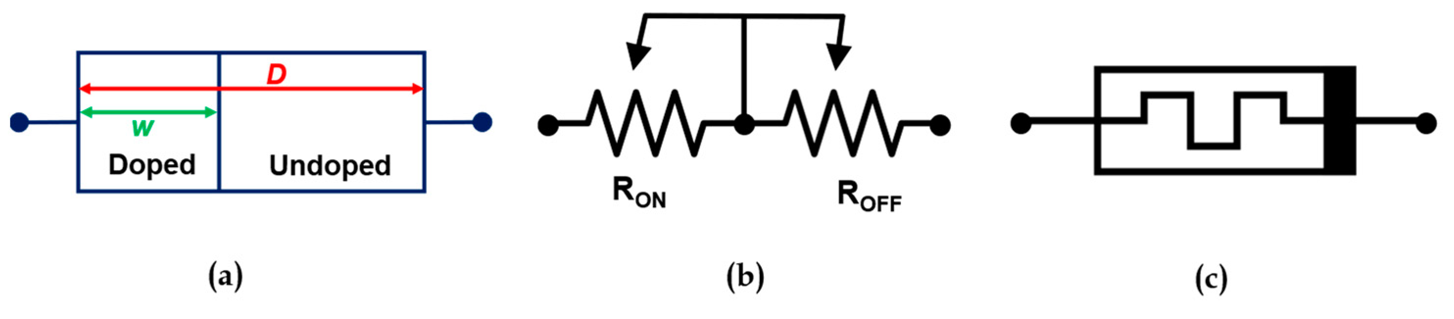
2.3. IMT Material as a Selector

The transition between insulating and metallic states in certain materials, known as the insulator–metal transition (IMT) or metal–insulator transition (MIT), has raised significant attention in electronics. This property transition, also known as the Mott transition, denotes a temporary change in a material’s electrical resistivity and optical characteristics under external excitement, such as heat, pressure, and electrical or magnetic fields. The Mott transition is a distinctive feature of some materials because, as explained by N.F. Mott, it originates from the complex interplay of electron–electron interactions, representing a fundamental twist from the more straightforward metal–semiconductor transitions predicted by conventional band theory [26]. For instance, IMT can be observed in vanadium dioxide (VO2), which is a material with a well-documented history of this transition. First discovered by F. J. Morin in 1959, the IMT in VO2 was noted to occur near a critical temperature point, referred to as the Néel temperature [27]. The substance undergoes a phase change from a nonconducting monoclinic structure phase to a conducting rutile structure phase at a relatively low thermal threshold of about 67 °C, making it an excellent material for applications operating not very far from room temperature. The resistivity change versus temperature is illustrated in Figure 6 [28].
Inducing the IMT in materials like VO2 can be achieved through various stimuli, including thermal, electrical field, optical, or mechanical stress, and each can provide specific characteristics and functional behaviors to devices. Also, the material’s environment or the surface it is attached to can significantly influence the temperature at which the material changes and how much its electrical resistance changes [29].

3. Simulation Models

This article investigates and studies the SPICE simulation models of the 1S1R ReRAM array configuration. The selector is an IMT resistor that is made of VO2. The memory cells are TiO2 film memristors. In the following subsections, we demonstrate the simulation models of both the selector and the memory element that are used in the simulations we report in this paper.

3.1. IMT Model

IMT devices can be effectively modeled as volatile memristive systems. These systems are two-terminal devices with resistance that varies based on the input registered history and the current state. Notably, volatile memristors can only maintain their altered resistance while connected to the stimuli; when disconnected, their resistance returns to its original state.
IMT devices are represented through a state equation and an output equation in this approach. The output equation is follows:
I = V R T t ,
which links the device’s internal state with its observed output. Meanwhile, the state equation is as follows:
d T ( t ) d t = r ( T t , V ) ,
which describes the IMT device’s internal dynamics. Specifically, the output equation defines how the input voltage (V) and output current (I) relate to the changing resistance. The state variable, T(t), represents the device’s internal state.
One key aspect of the output equation is that the resistance is a function of the internal state variable and varies with time and temperature. This characteristic distinguishes IMT devices from most others, where resistance is typically constant. On the other hand, the state equation reflects how the state variable evolves over time in response to the device’s input—namely the voltage across the device. Our model, introduced for the first time in [30], builds upon and simplifies the one presented in reference [31], incorporating the hysteresis of IMT devices.

3.1.1. Temperature Evolving

The model captures the thermal behavior of IMT devices by simplifying the complex heat conduction process into a lumped thermal model. This model is presented as a first-order linear differential equation:
T T a m b = τ t h V · I d T t d t + I 2 · R I M T C t h ,
which accounts for instantaneous temperature changes, denoted by dT(t)/dt, and includes a term representing the cooling effect, where Tamb is the ambient temperature and τth is the thermal time constant. This term reflects heat loss to the surroundings and the system’s thermal response.
Another critical aspect is the (I2·RIMT)/Cth term, representing the rate of temperature increase due to Joule heating, where I is the current, RIMT is the resistance, and Cth is the thermal capacitance of the system. This model balances heat generation and dissipation, providing a mathematical framework to predict temperature changes in IMT devices under various conditions.

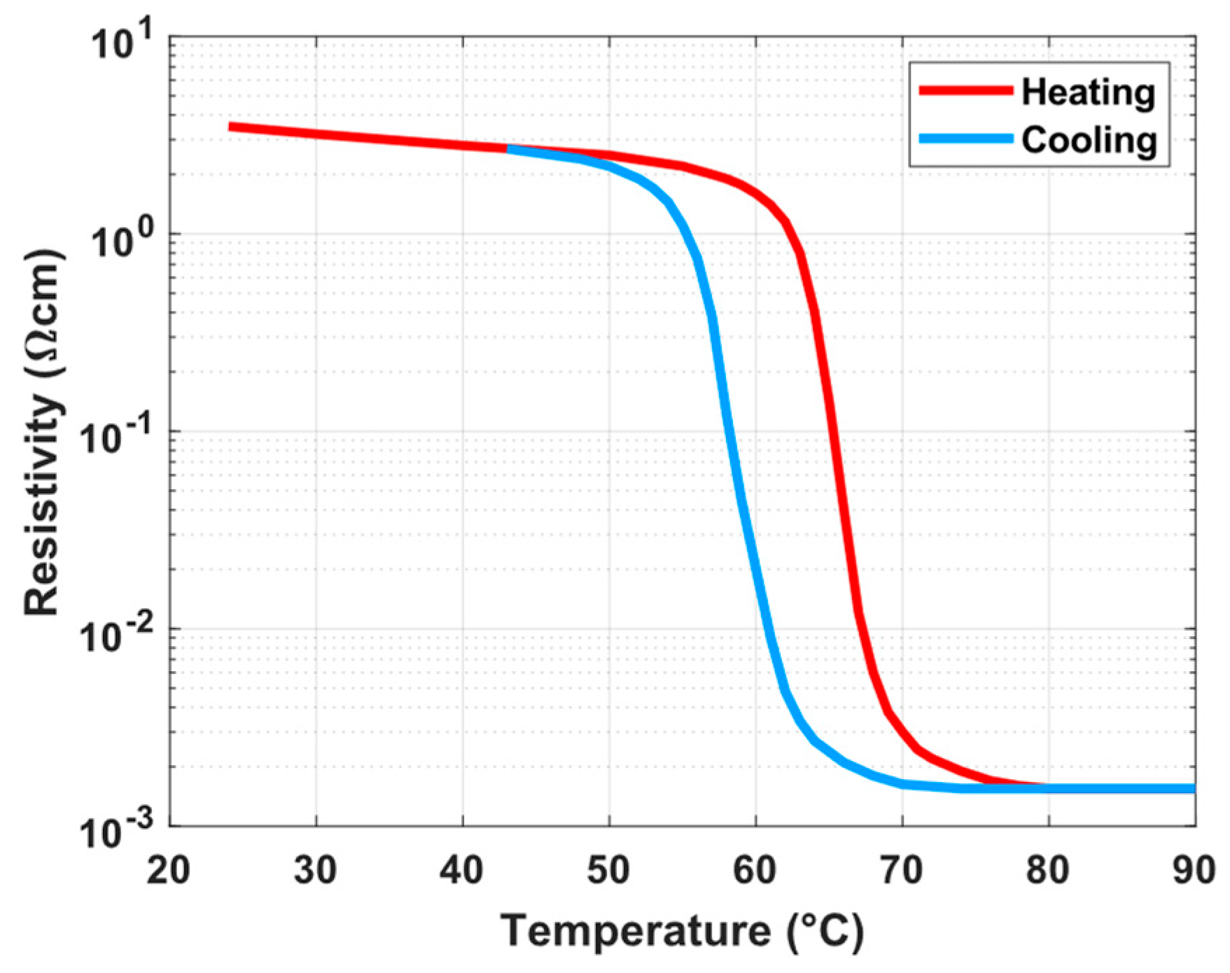
3.1.2. Resistance Change with Temperature

The resistance of the IMT device as a function of temperature can be accurately described using sigmoid and exponential functions. This relationship is as follows:
R I M T T = R M · e B M T T f + R I · e B I T T o R M · e B M T T f 1 + e T T I M T T x ,
which includes different resistances (RM and RI) for the metallic and insulation states, temperature coefficients, (BM and BI), and specific temperatures, (To and Tf), that mark the start and end of the phase transition. TIMT represents the midpoint of the phase change, with distinct values for the heating and cooling phases. Tx indicates the transition sharpness.

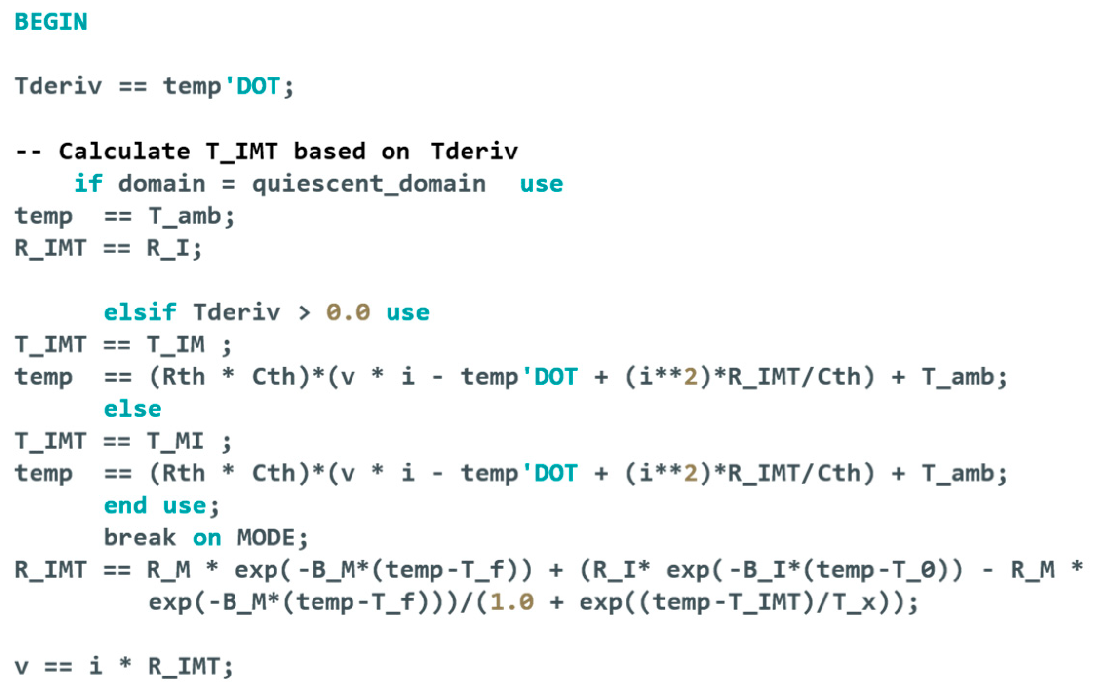
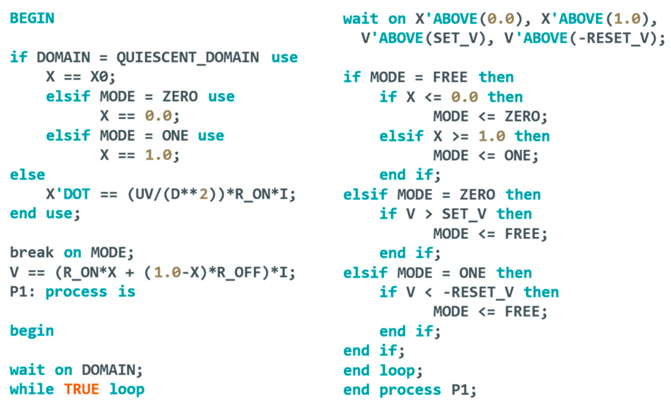
3.1.3. Simulation Model Code

While our model is based on the approach in [31], which used Verilog-A and did not consider the hysteresis between the heating and cooling phases, it addresses a gap in the existing literature. Our model distinguishes three states of the IMT device: heating, cooling, and equilibrium, the latter being when the temperature remains constant. These states are determined by the temperature history, represented by the state variable T(t). Mathematically, we use the time derivative of temperature, dT(t)/dt, as shown in the code snippet in Figure 7.
A positive derivative indicates a heating state, where TIMT in the temperature equation is replaced with TIM (the midpoint of the heating curve). Conversely, a negative derivative signifies a cooling state, and TIMT is replaced with TMI (the midpoint of the cooling curve). A zero derivative denotes a state of thermal equilibrium. Additionally, our model includes an output signal that records the state change history during simulations, allowing this data to be visualized in a waveform viewer.

3.2. Memristor Model

In 2008, researchers from HP Labs reported on a two-terminal (TiO2) device that depicts the memristive characteristics published by L. Chua in 1971 [6,32]. We used a memristor model available in the literature with minor modifications [33]. The proposed model in the article “Hybrid Dynamical Systems for Memristor Modelling” introduces an innovative approach to simulate memristors, leveraging the framework of the hybrid dynamic system implemented by a finite set of modes. The model is based on a set of first-order, time-invariant equations for a voltage-controlled, one-port memristive system. There are two layers in the TiO2 film. One of them has high resistance TiO2 (undoped layer), and the other layer is full of oxygen vacancies with low electric resistance (doped layer), as illustrated in Figure 8.
The state variable x = (w/D) depicts the past or the history of the device:
M w = R O N · w D + R O F F · 1 w D , w h e r e 0 w D 1.0 ,
where applying an external bias voltage to the device generates an electric field that drives the positively charged oxygen vacancies from the doped layer to the undoped layer, altering the length, w. This adjustment results in a change in the device’s overall resistivity. When the doped area spans the entire width D (i.e., w/D = 1.0), the device exhibits a low total resistivity, indicated as RON. Conversely, if the undoped area covers the full width, D (i.e., w/D = 0), the device’s total resistivity is high, indicated as ROFF. This behavior illustrates the memristor’s memory effect, where it retains its resistivity level even after the removal of the bias voltage. The term µv represents the ion mobility in the linear ion-drift model that is given by the following:
d x ( t ) d t = μ v · R O N D 2 · i t , w h e r e x t = w ( t ) D ,
where the device’s physical width is designated as D. The variable width, labeled w, fluctuates between 0 and D. Consequently, the state variable, x, dependent on w, falls within the range {0,1}. This setup enables the identification of three distinct operational modes. The memristance in
v ( t ) = M ( w ( t ) ) · i t
becomes RON when the width w reaches its maximum value of D, defining mode ONE (where the state variable x equals 1). Conversely, when w is at its minimum value of 0, the memristance shifts to ROFF, known as mode ZERO (with x at 0). In situations where w varies between 0 and D, the memristance lies between RON and ROFF, characterizing this as the FREE mode.
The model code is simple and straightforward; a code snippet of the model is shown in Figure 9. Both Equations (6) and (7) are included in the model and displayed in the code. The code consists of three main parts: the domain part, where the transition between the domains is defined; the process part, which describes the changes of the state mode; and the wait part, which checks if any critical voltages are met.

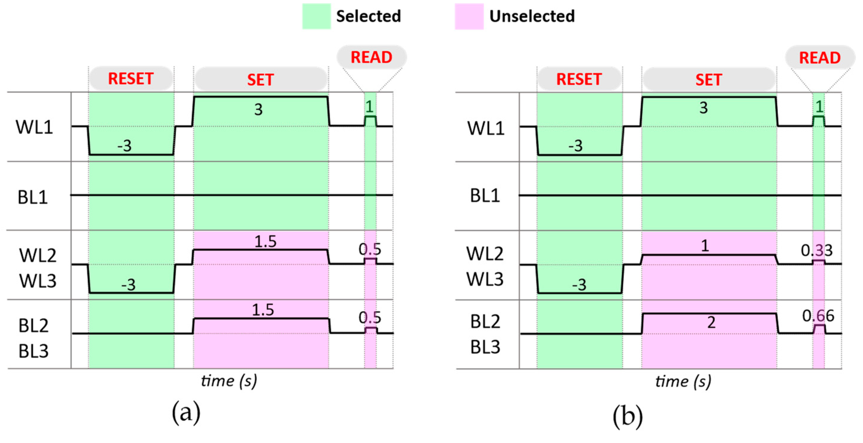
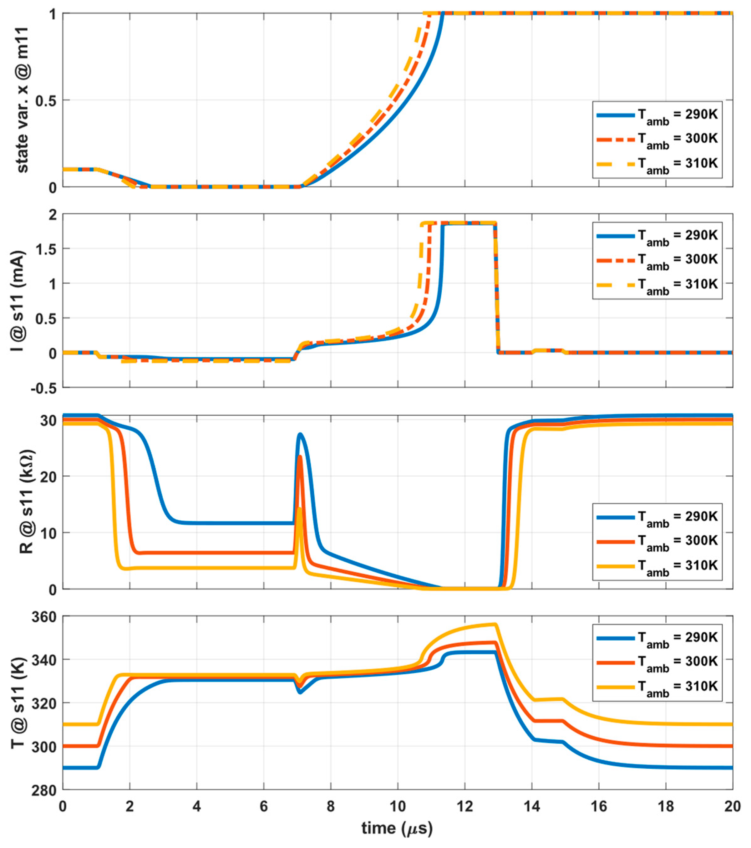
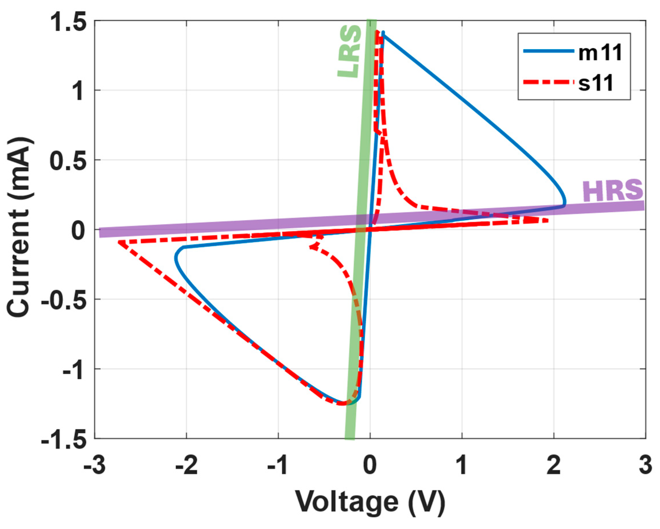
4. Simulation Setup and Results

The simulations and results discussed in this section pertain to a 3 × 3 ReRAM crossbar array. This specific array size was chosen to simplify the analysis and avoid the complexities inherent in larger arrays. Despite its smaller scale, a 3 × 3 array provides sufficient insight to effectively replicate and understand the behavior and operational characteristics of ReRAM memory systems. It is important to note that larger memory arrays introduce increased nonlinearities, thus demanding a more comprehensive and detailed study.
The software that was used for the simulation of the ReRAM crossbar array is PartQuest Explore, which is a design, analysis, and simulation software for multi-domain systems, including electro-thermal systems, and both SPICE and VHDL-AMS models are supported [34]. The circuit schematic is presented in Figure 10. The wordlines, WL, and bitlines, BL, are biased with a programmable voltage pulse source where the rise time, fall time, pulse width, and pulse value can be changed. The resistors, RLine, are the resistances between two adjacent junctions or between a cell and voltage source and are assumed to be 3Ω. Rsense refers to the sense resistor used to determine the state of a memory cell by measuring the voltage drop through it; here, it is set to 1.5 kΩ, and the voltage drop is amplified to enhance the accuracy and detectability of small voltage variations indicative of the memory cell’s state during a READ operation.
In this example, the SET voltage is 3 V (writing 1), the RESET voltage is −3 V (erasing or writing 0), and the READ voltage is 1 V. The biasing schemes are applied to the wordlines and bitlines to erase the content of all memory cells and ensure a clean state for data storage, which is followed by a SET operation only on one memory cell (m11), as shown in Figure 11. This is achieved by applying the RESET voltage of −3 V across the relevant lines, then writing 1 only on the m11 memory cell, and then reading the status of m11 only. The selection of these specific voltages is critical, as they ensure optimal performance. A higher voltage, for instance, might speed up the writing process but could also lead to very high temperatures on the IMT selectors.
To study the effect of the selector on the memory cell’s performance, we focused on altering two critical parameters in the selector model: Tamb and TIMT (average value of TIM + TMI). Tamb is a crucial factor as it represents the operating environmental conditions of the memory cell, which can drastically affect its stability and lifespan. On the other hand, TIMT is selected for its direct influence on the memory speed and the amount of Joule heating required to switch the selector status. The effect of changing Tamb by ±10 K on the memory cell and the selector is illustrated in Figure 12, and the effect of changing TIMT by ±5 K on the memory cell and the selector is shown in Figure 13.
In the m11 memristor, the state variable x begins at 0.1, reflecting all memristors’ initial conditions in the circuit, and this can be set in the simulator. It then drops to 0.0, indicating a reset to the HRS, and later reaches its maximum at 1.0 when m11 is set to the LRS, as observed in Figure 12 and Figure 13. It is noted that higher ambient temperatures accelerate the transition from HRS to LRS, while higher critical temperatures slow it down. The fluctuations in resistance and temperature graphs (short dips and peaks) correspond to brief lags in memristor and selector responses during memory cell status changes.
Figure 14 presents the V-I curve that illustrates the electrical characteristics of the memory cell and its associated selector. This graph explains how these components behave under varying electrical conditions. Notably, two critical lines are highlighted on the graph: the LRS and the HRS. The LRS line represents the state where the memory cell exhibits low resistance, typically associated with the “on” or “1” state, facilitating higher current flow. In contrast, the HRS line depicts the memory cell in a high resistance state, analogous to the “off” or “0” state, where the current flow is significantly reduced.
To address the issue of sneak path currents in crossbar memory arrays, Table 1 presents data on current flow through each memory cell, highlighting the selector’s role in minimizing these currents. This simulation data, gathered during the “write 1” and “read” operations, examines the effects of different biasing schemes, namely the one-half and one-third voltage biasing, both with and without the selector present. The notable differences in current values highlight the importance of these schemes and the selector in enhancing memory operation efficiency and reducing energy consumption.

5. Conclusions

This research advances the understanding of resistive random access memory ReRAM crossbar arrays, particularly highlighting the integration with insulator–metal transition (IMT) based selectors. Through detailed SPICE simulations of a 3 × 3 ReRAM array with vanadium dioxide selectors and titanium dioxide film memristors, we have demonstrated how variables, like ambient temperature and critical IMT temperatures, influence memory behavior. The models used in the simulation are explained and written in VHDL-AMS language. We demonstrated the critical role of the IMT selector in mitigating sneak path currents and enhancing the ReRAM operation. These selectors are self-excited by the Joule heating dissipation. Additionally, this study confirms the effectiveness of appropriate voltage settings and biasing schemes in controlling sneak path currents, with significant implications for memory dynamics. This work contributes to the field, offering an insight into ReRAM’s selectors operational dynamics and paving the way for more efficient and reliable non-volatile memory designs.

Author Contributions

Conceptualization, simulation, and writing, M.D.; supervision, and review, L.P. All authors have read and agreed to the published version of the manuscript.

Funding

This research received no external funding.

Data Availability Statement

The data presented in this study are available on request from the corresponding author.

Conflicts of Interest

The authors declare no conflicts of interest.

References

  1. Chen, F.; Koufaty, D.A.; Zhang, X. Understanding Intrinsic Characteristics and System Implications of Flash Memory Based Solid State Drives. SIGMETRICS Perform. Eval. Rev. 2009, 37, 181–192. [Google Scholar] [CrossRef]
  2. ReRAM. Available online: https://www.fujitsu.com/jp/group/fsm/en/products/reram/ (accessed on 25 October 2023).
  3. Heyman, K. ReRAM Seeks to Replace NOR. Available online: https://semiengineering.com/reram-seeks-to-replace-nor/ (accessed on 25 October 2023).
  4. Wainstein, N.; Adam, G.; Yalon, E.; Kvatinsky, S. Radiofrequency Switches Based on Emerging Resistive Memory Technologies—A Survey. Proc. IEEE 2021, 109, 77–95. [Google Scholar] [CrossRef]
  5. Dittmann, R.; Menzel, S.; Waser, R. Nanoionic Memristive Phenomena in Metal Oxides: The Valence Change Mechanism. Adv. Phys. 2021, 70, 155–349. [Google Scholar] [CrossRef]
  6. Strukov, D.B.; Snider, G.S.; Stewart, D.R.; Williams, R.S. The Missing Memristor Found. Nature 2008, 453, 80–83. [Google Scholar] [CrossRef] [PubMed]
  7. Bai, Y.; Wu, H.; Wang, K.; Wu, R.; Song, L.; Li, T.; Wang, J.; Yu, Z.; Qian, H. Stacked 3D RRAM Array with Graphene/CNT as Edge Electrodes. Sci. Rep. 2015, 5, 13785. [Google Scholar] [CrossRef] [PubMed]
  8. Shang, Y.; Ohsawa, T. Accurate Measurement of Sneak Current in ReRAM Crossbar Array with Data Storage Pattern Dependencies. In Proceedings of the 2019 International Symposium on VLSI Technology, Systems and Application (VLSI-TSA), Hsinchu, Taiwan, 22–25 April 2019; pp. 1–2. [Google Scholar]
  9. Demin, V.A.; Surazhevsky, I.A.; Emelyanov, A.V.; Kashkarov, P.K.; Kovalchuk, M.V. Sneak, Discharge, and Leakage Current Issues in a High-Dimensional 1T1M Memristive Crossbar. J. Comput. Electron. 2020, 19, 565–575. [Google Scholar] [CrossRef]
  10. Kannan, S.; Rajendran, J.; Karri, R.; Sinanoglu, O. Sneak-Path Testing of Crossbar-Based Nonvolatile Random Access Memories. IEEE Trans. Nanotechnol. 2013, 12, 413–426. [Google Scholar] [CrossRef]
  11. Chen, A. Memory Selector Devices and Crossbar Array Design: A Modeling-Based Assessment. J. Comput. Electron. 2017, 16, 1186–1200. [Google Scholar] [CrossRef]
  12. Lekshmi Jagath, A.; Kumar, T.N.; Almurib, H.A.; Jinesh, K.B.P. Analytical Modelling of Tantalum/Titanium Oxide-Based Multi-layer Selector to Eliminate Sneak Path Current in RRAM Arrays. IET Circuits Devices Syst. 2020, 14, 1092–1098. [Google Scholar] [CrossRef]
  13. Shi, L.; Zheng, G.; Tian, B.; Dkhil, B.; Duan, C. Research Progress on Solutions to the Sneak Path Issue in Memristor Crossbar Arrays. Nanoscale Adv. 2020, 2, 1811–1827. [Google Scholar] [CrossRef]
  14. Seok, J.Y.; Song, S.J.; Yoon, J.H.; Yoon, K.J.; Park, T.H.; Kwon, D.E.; Lim, H.; Kim, G.H.; Jeong, D.S.; Hwang, C.S. A Review of Three-Dimensional Resistive Switching Cross-Bar Array Memories from the Integration and Materials Property Points of View. Adv. Funct. Mater. 2014, 24, 5316–5339. [Google Scholar] [CrossRef]
  15. Ravi, V.; Singh, S.; Sofana Reka, S. Memristor-Based 2D1M Architecture: Solution to Sneak Paths in Multilevel Memory. Trans. Emerg. Telecommun. Technol. 2021, 32, e4143. [Google Scholar] [CrossRef]
  16. Li, Y.; Ang, K.-W. Hardware Implementation of Neuromorphic Computing Using Large-Scale Memristor Crossbar Arrays. Adv. Intell. Syst. 2021, 3, 2000137. [Google Scholar] [CrossRef]
  17. Zhang, L. Study of the Selector Element for Resistive Memory. Available online: https://lirias.kuleuven.be/1733031?limo=0 (accessed on 20 December 2023).
  18. Li, Y.; Gong, Q.; Li, R.; Jiang, X. A New Bipolar RRAM Selector Based on Anti-Parallel Connected Diodes for Crossbar Applications. Nanotechnology 2014, 25, 185201. [Google Scholar] [CrossRef]
  19. Lee, J.; Lee, S.; Kwak, M.; Choi, W.; Mosendz, O.; Hwang, H. Enhanced Switching Characteristics of an Ovonic Threshold Switching Device with an Ultra-Thin MgO Interfacial Layer. IEEE Electron. Device Lett. 2022, 43, 220–223. [Google Scholar] [CrossRef]
  20. Narayanan, P.; Burr, G.W.; Shenoy, R.S.; Stephens, S.; Virwani, K.; Padilla, A.; Kurdi, B.N.; Gopalakrishnan, K. Exploring the Design Space for Crossbar Arrays Built With Mixed-Ionic-Electronic-Conduction (MIEC) Access Devices. IEEE J. Electron. Devices Soc. 2015, 3, 423–434. [Google Scholar] [CrossRef]
  21. Farjadian, M.; Shalchian, M. Modeling and Design of a Mott Selector for a ReRAM-Based Non-Volatile Memory Cell in a Crossbar Architecture. J. Comput. Electron. 2022, 21, 535–549. [Google Scholar] [CrossRef]
  22. Jeon, D.S.; Dongale, T.D.; Kim, T.G. Low Power Ti-Doped NbO2-Based Selector Device with High Selectivity and Low OFF Current. J. Alloys Compd. 2021, 884, 161041. [Google Scholar] [CrossRef]
  23. Cha, E.; Woo, J.; Lee, D.; Lee, S.; Hwang, H. Selector Devices for 3-D Cross-Point ReRAM. In Proceedings of the 2014 IEEE International Symposium on Circuits and Systems (ISCAS), Melbourne, Australia, 1–5 June 2014; pp. 428–431. [Google Scholar]
  24. Dai, Y.; Tao, F.; Qi, M. Design of Selector-Based Insulator-Metal Transition Model for TiO2 Bipolar Resistive Random Access Memory. J. Appl. Phys. 2019, 126, 075705. [Google Scholar] [CrossRef]
  25. Nandi, S.K.; Liu, X.; Venkatachalam, D.K.; Elliman, R.G. Threshold Current Reduction for the Metal–Insulator Transition in NbO2-x-Selector Devices: The Effect of ReRAM Integration. J. Phys. D Appl. Phys. 2015, 48, 195105. [Google Scholar] [CrossRef]
  26. Mott, N.F. Metal-Insulator Transition. Rev. Mod. Phys. 1968, 40, 677–683. [Google Scholar] [CrossRef]
  27. Morin, F.J. Oxides Which Show a Metal-to-Insulator Transition at the Neel Temperature. Phys. Rev. Lett. 1959, 3, 34–36. [Google Scholar] [CrossRef]
  28. Darwish, M.; Neumann, P.; Mizsei, J.; Pohl, L. Electro-Thermal Simulation of Vertical VO2 Thermal-Electronic Circuit Elements. Energies 2020, 13, 3447. [Google Scholar] [CrossRef]
  29. Yang, Z.; Ko, C.; Ramanathan, S. Oxide Electronics Utilizing Ultrafast Metal-Insulator Transitions. Annu. Rev. Mater. Res. 2011, 41, 337–367. [Google Scholar] [CrossRef]
  30. Darwish, M.; Pohl, L. SPICE Modeling of Insulator-Metal Transition Devices with Hysteresis. In Proceedings of the 2023 29th International Workshop on Thermal Investigations of ICs and Systems (THERMINIC), Budapest, Hungary, 27–29 September 2023; pp. 1–5. [Google Scholar]
  31. Amer, S.; Hasan, M.S.; Adnan, M.M.; Rose, G.S. SPICE Modeling of Insulator Metal Transition: Model of the Critical Temperature. IEEE J. Electron Devices Soc. 2019, 7, 18–25. [Google Scholar] [CrossRef]
  32. Chua, L. Memristor-The Missing Circuit Element. IEEE Trans. Circuit Theory 1971, 18, 507–519. [Google Scholar] [CrossRef]
  33. Haase, J.; Lange, A. Hybrid Dynamical Systems for Memristor Modelling an Approach Avoiding the Terminal-State Problem. In Proceedings of the 2013 Forum on Specification and Design Languages (FDL), Paris, France, 24–26 September 2013; pp. 1–6. [Google Scholar]
  34. PartQuestTM Explore|Design, Modeling, Simulation and Analysis. Available online: https://explore.partquest.com/ (accessed on 13 December 2023).
Figure 1. The structure of crossbar arrays: (a) the 3D physical configuration; (b) circuit diagram of a memristive crossbar array.
Electronicmat 05 00002 g001
Figure 2. Schematic I-V curves of (a) unipolar switching and (b) bipolar switching.
Electronicmat 05 00002 g002
Figure 3. Illustration of sneak path current in crossbar array with resistive switching memory cells during WRITE or READ operations.
Electronicmat 05 00002 g003
Figure 4. The two typical types of bias schemes: (a) the one-half (½) bias scheme and (b) the one-third (⅓) bias scheme.
Electronicmat 05 00002 g004
Figure 5. ReRAM arrays based on selector type: (a) 1T1R and (b) 1S1R.
Electronicmat 05 00002 g005
Figure 6. The resistivity versus temperature of vanadium dioxide.
Electronicmat 05 00002 g006
Figure 7. VHDL-AMS IMT model code snippet.
Electronicmat 05 00002 g007
Figure 8. The memristor’s (a) structure, (b) equivalent circuit, and (c) symbol.
Electronicmat 05 00002 g008
Figure 9. VHDL-AMS memristor model code snippet.
Electronicmat 05 00002 g009
Figure 10. 3 × 3 ReRAM crossbar array circuit schematic.
Electronicmat 05 00002 g010
Figure 11. How to erase all cells, WRITE 1 on m11, and READ m11 using both (a) the one-half (b) and the one-third bias schemes.
Electronicmat 05 00002 g011
Figure 12. The behavior of m11 and s11 at different ambient temperatures.
Electronicmat 05 00002 g012
Figure 13. The behavior of m11 and s11 at different critical temperatures.
Electronicmat 05 00002 g013
Figure 14. The V-I characteristics of both memory cell, m11, and IMT selector, s11, indicating HRS and LRS operation regions.
Electronicmat 05 00002 g014
Table 1. Current flow on each memory cell during writing 1 and reading processes.
OperationWriting 1 at m11Reading from m11
Biasing Scheme1/21/31/21/3
Selectorwithoutwithwithoutwithwithoutwithwithoutwith
Main Current at m11200318702062189066731.61687.331.96
Sneak Current atm12, m13320.234.18124.322.39208.111.3544.67.47
m21, m31−99.4−27.08−110−38.49−269.25−365.84
m22, m23, m32, m33−25.7−1.05−60−21.25−16−0.349−21.8−7.04
All values are in µA.
Disclaimer/Publisher’s Note: The statements, opinions and data contained in all publications are solely those of the individual author(s) and contributor(s) and not of MDPI and/or the editor(s). MDPI and/or the editor(s) disclaim responsibility for any injury to people or property resulting from any ideas, methods, instructions or products referred to in the content.

