1. Introduction
Perovskite materials are a gold mine for materials science. They are functional compounds with tailor-made characteristics [
1,
2,
3]. Indeed, these materials have shown very rich phase diagrams and a great ability to absorb strong nonstoichiometric effects, making it possible to modulate, among others, their electronic, magnetic and optical properties [
4,
5].
Moreover, depending on their chemical compositions and crystallographic structures, these materials can be considered as a superconducting material at relatively high temperatures [
6]. Additionally, they can convert heat or mechanical pressure into an electric current [
7], accelerate chemical reactions or even produce an electric current upon exposure to light [
8,
9].
Therefore, perovskite materials have promising properties for many technological applications such as modern electronics (memories, capacitors, ultrafast electronics, etc.), fuel cells and transparent ceramics, and photovoltaic cells [
10,
11]. These materials can be organic, inorganic or hybrid. The methods of their elaboration are also diverse and depend on the targeted properties, the production cost and the expected applications [
12]. In the photovoltaic field, the chemical method is dominant for the deposition of thin layers of these materials. The organic and hybrid varieties are the most widely studied in the literature. In fact, the development of solar cells containing hybrid or organic perovskites as light-absorbing materials has been extremely fast and has achieved record yields, competing with the records of silicon-based solar cells. This success is due to the fact that hybrid perovskites have remarkable optical and electronic properties, combining the advantages of organic and inorganic semiconductors. Although these choices are motivated by the ease, the speed and the cost of the elaboration, the stability of the films as well as the toxicity of certain elements used remain weak points [
13].
The use of inorganic materials may circumvent these problems. Notably, it is easier to control the stoichiometry or non-stoichiometry of these compounds when they are prepared in a vacuum. This non-stoichiometry, for example, can be important to improve the optical, magnetic and electrical characteristics of perovskite materials [
14,
15]
Among inorganic materials for photovoltaic applications are compounds based on lanthanum and manganese, which are mainly prepared by chemical means [
16,
17,
18]. However, the perovskite structure is generally preferred to obtain the best performance, and notably, the highest electrical efficiency. Indeed, in addition to the good mobility of electrical charges [
19], perovskite structures have other advantages such as a good absorption of light [
20].
This paper reports research on the use of lanthanum manganite thin films deposited by a reactive magnetron co-sputtering process. The objective of this study is to understand how the perovskite structure induced by annealing can contribute to the evolution of the structural, optical and electrical properties of this oxide.
A singularity of this work lies in the choice of the stoichiometry of the LMO films and the use of simple analytical techniques, especially the use of a capacitance meter with a mercury probe to study the electrical properties (capacitance, photocurrent) of the LMO film. Indeed, we made the choice to deposit slightly more Mn than La in order to evaluate the effect of probable induced lanthanum and/or oxygen deficiencies in the film on the different characteristics mentioned above.
2. Experiments
LMO thin films were deposited by co-sputtering of La (purity 99.9 at.%, diameter 50 mm, thickness 3 mm) and Mn (purity 99.9 at.%, diameter 50 mm, thickness 3 mm) targets in Ar and O2 gas mixture. Such a deposition technique easily allowed us to vary the stoichiometry ratio La/Mn by changing discharge power on both targets. The sputtering reactor is a 90 L cylinder Alcatel 604 SCM pumped down via a turbomolecular pump system that allows a residual vacuum below 10−4 Pa. Ar and O2 gas flow rates were controlled with Brooks flowmeters with QAr = 50 sccm and QO2 = 20 sccm, respectively. The total pressure (Ptot = 0.45 Pa) was measured with a Baratron manometer from MKS Instruments. N-doped silicon (orientation (111), phosphorus doped, 2 × 2 cm2) as well as fused silica slide (2 × 2 cm2) were used as substrates. Before each deposit, all our substrates have been cleaned with ethanol. The fused silica samples were additionally washed with soap and water. The rotating substrate holder was parallel to La and Mn sources at a distance of about 60 mm and all depositions were carried out at floating temperature (Tsubstrate < 70 °C).
The La and Mn targets were supplied with a pulsed direct current (DC) Advanced Energy dual generator, allowing us to control the discharge power. The discharge currents of La and Mn were fixed to 0.5 A and 0.34 A respectively. The discharge power was changed on both targets to adjust the film composition. The principal parameters used for the elaboration of our films are summarized in
Table 1.
After the synthesis of the film with the desired composition, annealing at different temperatures (400 °C, 500 °C, 600 °C and 700 °C) of the sample for 3 h was performed in a furnace under air. After each annealing, the structural, optical and electrical properties of the film were studied.
The chemical composition was determined via energy dispersive X-ray spectroscopy (EDS, Bruker nano, Berlin, Germany). These measurements were performed on the sample before annealing. The thickness of the film was measured by the step method with an Altisurf Profilometer (Altisurf 500) manufactured by Altimet. Before each measurement, the calibration of the experimental device was realized with a reference sample number, i.e., 787569, accredited by CETIM.
The structural characterization of coatings was performed by Bragg-Brentano configuration X-ray diffraction (XRD) using a BRUKER D8 focus diffractometer (Bruker AXS, Karlsruhe, Germany) with a cobalt X-ray tube (Co Kα1+α2 radiations λ = 0.178897 nm) and a LynxEye linear detector. Diffractograms were collected in air in an angle range 20–80° at a scan speed (2θ) of 0.1/s.
The evolution of the optical transmission as a function of the wavelength (200–1500 nm) was measured using a Lambda 950 spectrophotometer from Perkin Elmer. The determination of the optical gap of the film was deduced from the Tauc relation [
21].
The electrical properties of the LMO thin film were measured with a MDC 802C mercury probe capacitance meter (Materials Development Corporation). Only the film deposited on silicon was characterized. A metal oxide semiconductor (MOS) structure was mandatory for these measurements. Our film was therefore considered as an oxide. The operation of this tool was as follows: the sample to be characterized was placed on the support, upside down, i.e., the film to be characterized was at the bottom. The lever was lowered to be in contact with the silicon at the back of the sample. A drop of mercury rose through a capillary and came into contact with the film to be characterized. The surface of the drop-in contact with the film was very precisely controlled at 4.72 × 10
−3 cm
2. This probe was connected to an Agilent 4284A impedance analyzer. This device measures the complex impedance of the structure when subjected to a sinusoidal bias of the form U(t) = V
g(t) + s(t) with s(t) = S
0 sin(ωt). The gate bias voltage V
g(t), which varied in steps so that each measurement point was obtained at thermodynamic equilibrium, allowed us to probe the different operating regimes of the structure (accumulation, depletion and inversion). The small sinusoidal signal s(t) allowed us to extract the differential capacity, and thus, the C
tot versus V
g, named C–V curve. The flat band voltage V
FB could be deduced from the C–V curve using the flat band capacitance (C
FB) method [
22]. With this method, the ideal C
FB value is calculated from the film capacitance and the Debye length. After the value of C
FB is known, the value of V
FB can be deduced from the C–V curve data by interpolating between the closest V
g values. More details on this technique can be found in a previous paper [
23].
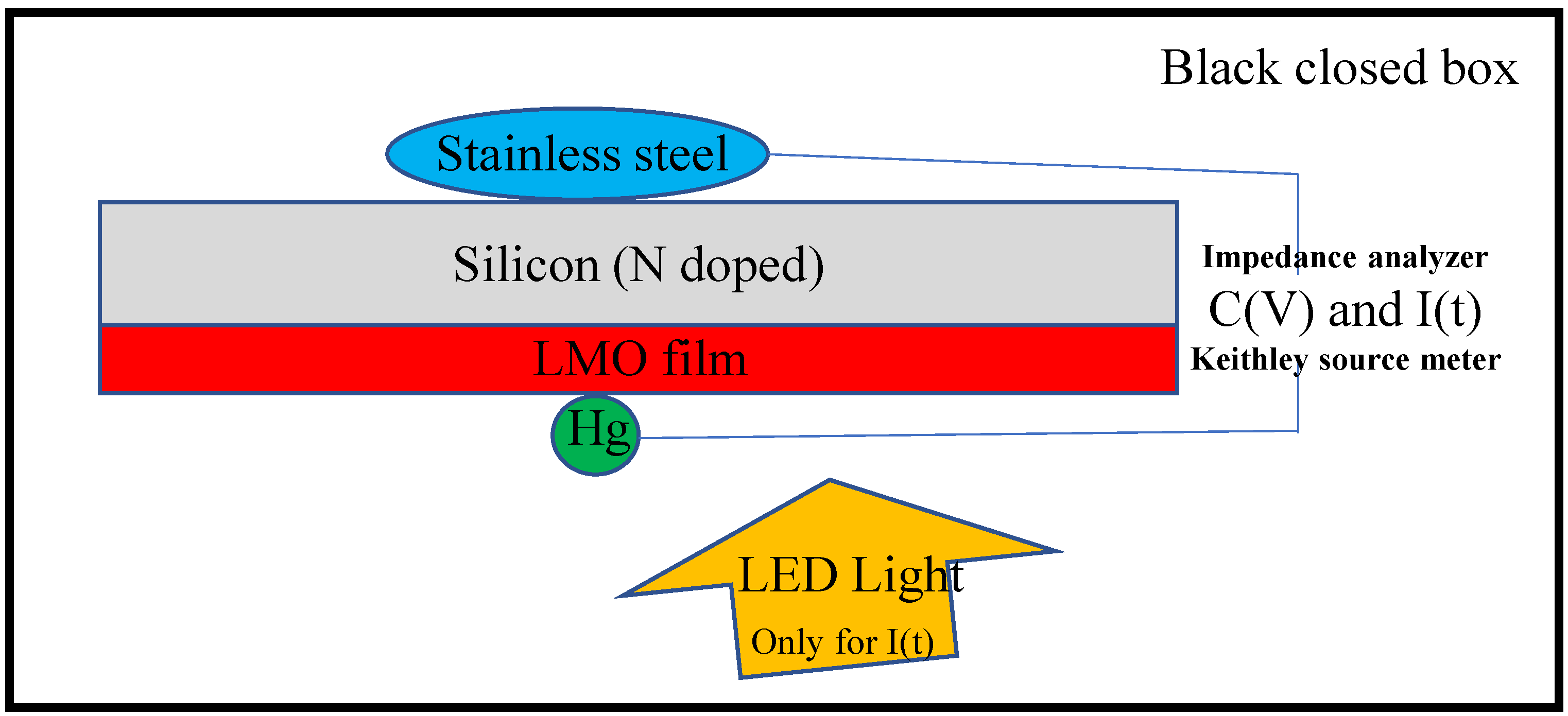
A simple LED lamp (from PREVAC, 1 W power) was introduced under the sample to evaluate the photoelectric effect of the film (see
Figure 1). Only the sample side with the deposition was illuminated. The operation consisted of measuring the current over a specific time in the dark (closed box during 1 min) and under illumination (closed box + LED light during 2 min) and in dark again during 1 min. The sample was polarized at −2 V during the measurements. This voltage was applied in order to create an electric field that would separate the electron-hole pair generated by the light in the film.
3. Results
The thickness of the studied films was determined to be 375 nm. The EDS elemental spectra of LMO film confirmed the presence of La and Mn in the film, with atomic percentages measured to be 48% and 52%, respectively.
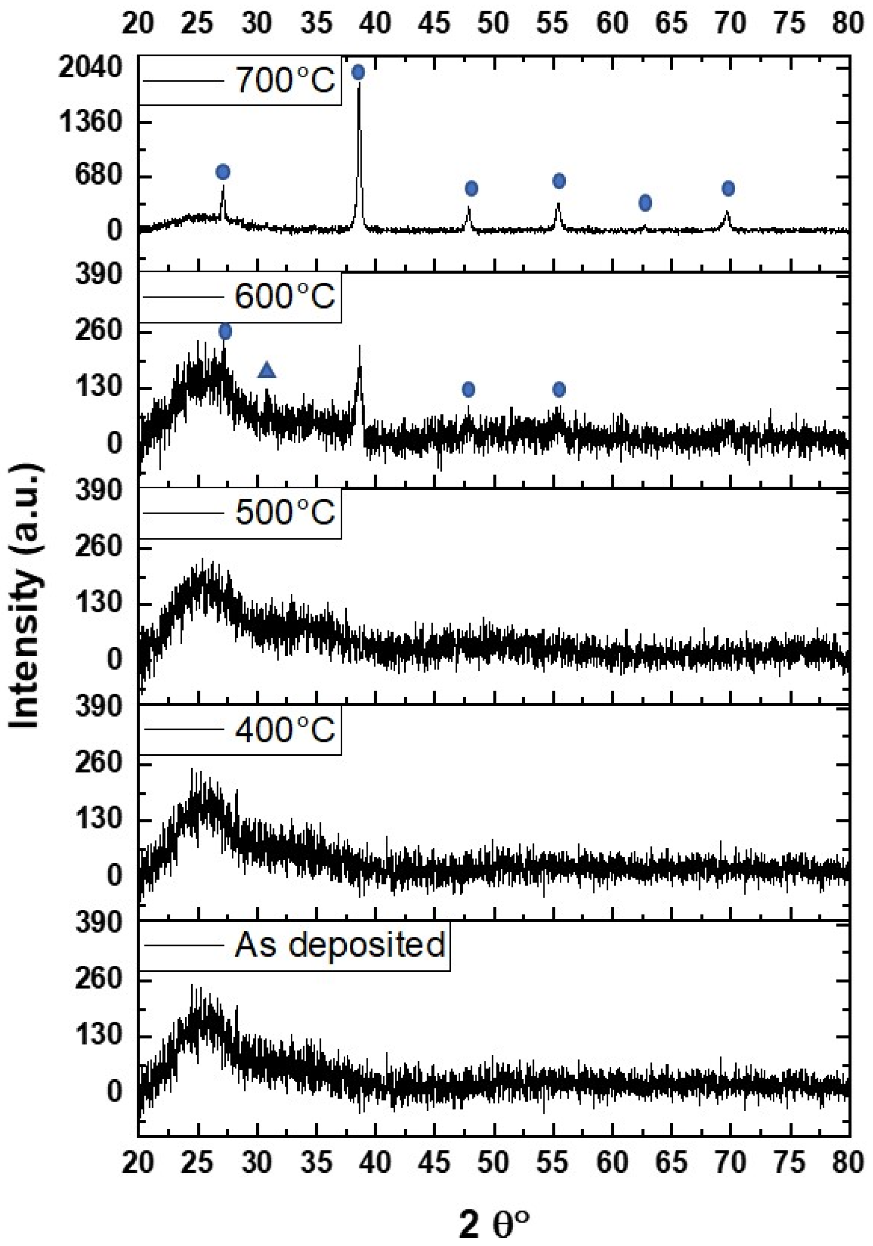
Figure 2 shows the XRD patterns of the LMO film versus annealing temperature. The as deposited film was amorphous and after annealing at 400 °C and 500 °C, and no significant peaks were detected. Film crystallization started at 600 °C, with a small diffraction peak at 38.22°. Other smaller peaks of lower intensity were also observed at 26.73°, 30.76°, 47.46° and 55.02° angles. Finally, after annealing at 700 °C, the peak at 30.76° vanished while the intensity of the other peaks increased and two new peaks (62.35° and 69.23°) appeared.
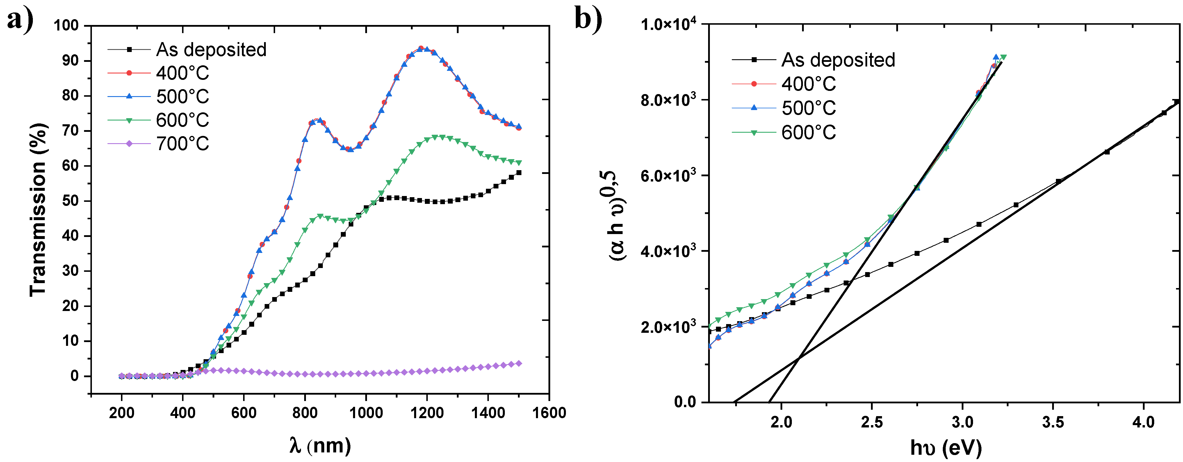
The optical spectra in
Figure 3a show that the transmission increased after annealing at 400 and 500 °C. The film transmittance then decreased after annealing at 600 °C, and finally, the film transmittance decreased drastically after annealing at 700 °C. From the transmittance drop region, we deduced the optical gap of each measurement. The latter was estimated from the intersection of the extrapolation of the curve giving (αhυ)
0.5 = f (hυ) with the x-axis [
21] (see
Figure 3b), where α is the absorption coefficient which can be calculated using the following formula:
. Here, h is Planck constant and ν is the frequency of the light. The optical gap was 1.74 eV before annealing but 1.93 eV after annealing at 400 °C, 500 °C and 600 °C. However, after annealing at 700 °C, the film was so opaque that it was impossible to determine the optical gap (<< 1 eV).
Figure 4a shows the capacitance measurements obtained before and after the different annealing processes. The dielectric constants (K) of each measurement, calculated from the maximum value of C
ox in accumulation, are also displayed. As shown, the shape of the curves is almost identical, and some evolutions are noted (
Figure 4b). First, the value of the dielectric constant (red curve) decreased after the first annealing at 400 °C (from K = 21 to K = 14), remained almost stable after the second annealing at about 500 °C (K = 13) and then increased strongly after annealing at 600 °C (K = 30) to finally drop after the last annealing at 700 °C (K = 7). Secondly, the flat band voltage V
FB (black curve) increased strongly after the annealing at 400 °C. Then, it decreased after the annealing at 500 °C and 600 °C. Finally, after annealing at 700 °C, V
FB rose again. The variation of V
FB was reflected by a shift of the C (V) curves to the right, as was the case after annealing at 400 °C and 700 °C, or to the left after annealing at 500 and 600 °C.
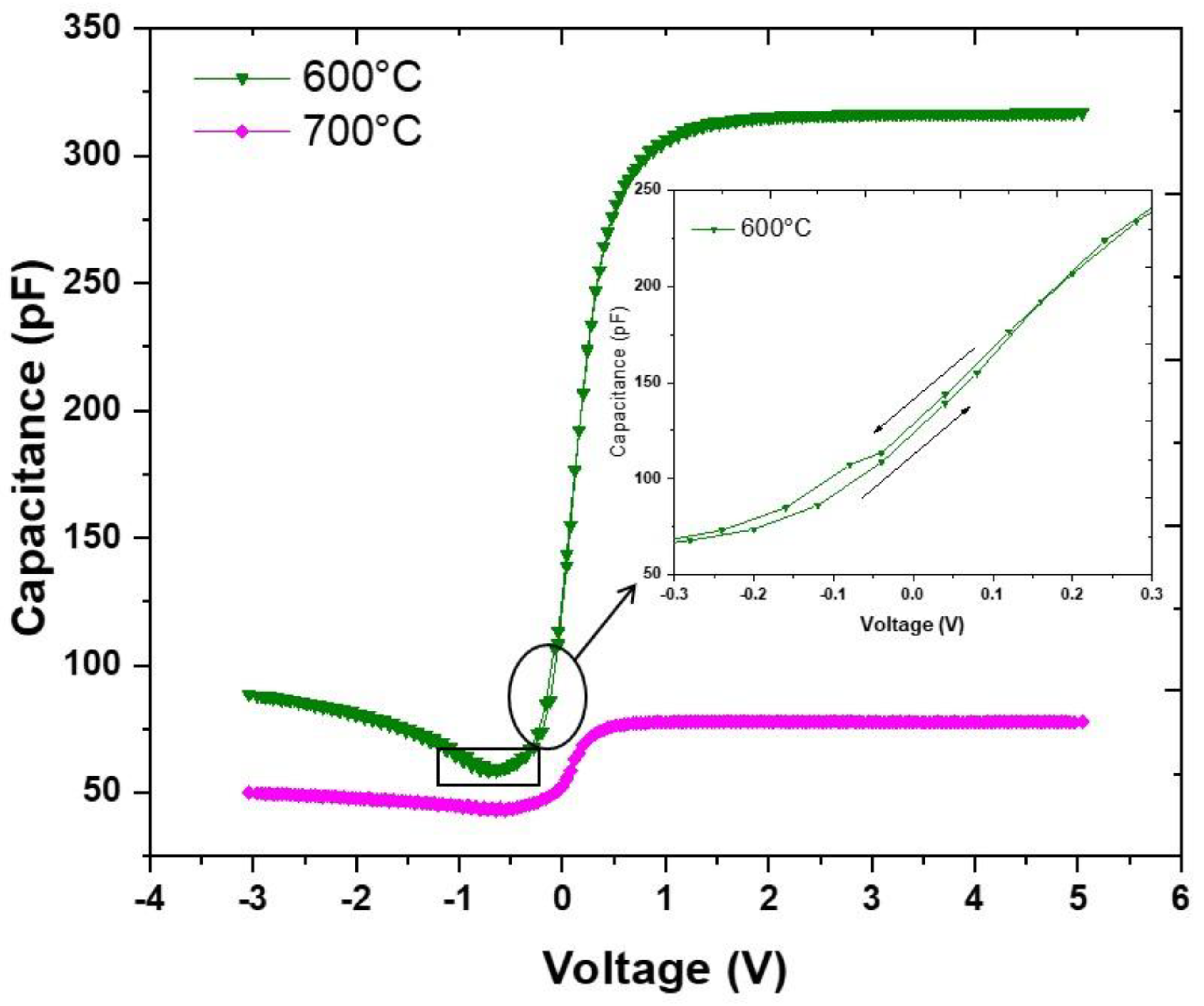
Figure 5 shows the measured C–V hysteresis characteristics of the LMO film after annealing at 600 and 700 °C. A zoom is performed to illustrate the extent of the hysteresis. A small dip (marked with a rectangle in
Figure 5) in the weak inversion region of the C–V curves is visible. This behavior only concerns the curve obtained at 600 °C; it disappeared after annealing at 700 °C.
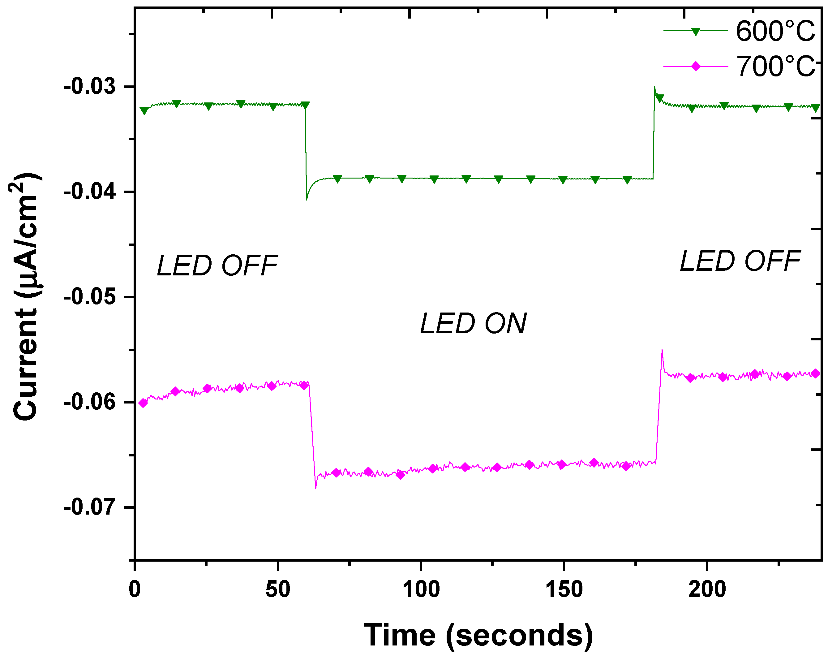
The exposure of the film to LED light, although very weak, led to the generation of a photocurrent.
Figure 6 shows the results obtained after annealing at 600 °C and 700 °C. We observe that the current through the film was almost stable at the beginning in the dark. This electric current represented the leakage current in the material and was measured in function of the illuminated surface (i.e., sample size of 4 cm
2). When the LED was turned on, the current increased and then returned to its initial value upon turning off the light. One evolution was noticed after the annealing at 700 °C. The value of the current in darkness increased from about −0.03 µA/cm
2 to −0.06 µA/cm
2. On the other hand, the variation of the current induced by the light seemed to be the same, i.e., approximately 2.5 nA/cm
2.
4. Discussion
Our films were all 375 nm thick. This thickness choice was justified by the objective of obtaining good photoelectric efficiency of our LMO layer. Indeed, it is generally accepted that if the thickness of the absorbing material is very small, then there will be a weak absorption of light and consequently a weak photogeneration of excitons. On the other hand, if the film is very thick, many charge carriers recombine before leaving this material [
24].
Concerning the XRD patterns of LMO films shown in
Figure 2, it is possible to appreciate that the diffraction peaks agree with the La
0.92MnO
3 [
25] structure. Accordingly, the peaks indicated by the circles represent the perovskite structure and the triangle indicates the Mn
3O
4 phase. These statements agree with the EDS results, where the La rate was slightly lower than Mn one. The peak at 2θ = 30.76° which was obtained at annealing temperature of 600 °C disappeared after annealing at 700 °C. This observation could be explained by the transformation of the Mn
3O
4 phase into Mn
5O
8 [
26].
The transmittance increase after the film was subjected to 400 °C thermal annealing could be attributed to the decrease in defects and the structural relaxation of the amorphous film. The second annealing at 500 °C did not change the optical transmission since the crystal structure of the film remained the same. After the third annealing at 600 °C, the transmittance decreased due to the onset of crystallization and changes in local bonding. This decrease in transmittance was even more apparent after the fourth annealing at 700 °C. Indeed, the transmittance decreased due to larger scale crystallization, with the formation of a few major crystalline phases. This trend of decreasing transmittance is consistent with theoretical models based on Rayleigh-Gans-Debye theory, according to which diffusion increases and transmittance decreases with increasing grain size [
27,
28].
The drop of the optical gap, in the form of the drop of the transmission after annealing at 700 °C, could be explained, in addition to what has already been mentioned, by amorphous-crystalline transformation, as observed from the XRD data and reported elsewhere [
29].
After the first and second annealing, the amorphous structure gave way to grains whose quantity increased with the annealing temperature. The dielectric loss caused by the grain boundaries increased, and consequently, the dielectric constant decreased (
Figure 4b). However, when the processing temperature was relatively high (600 °C), the number of grains was then reduced due to the coalescence of small grains into larger poly crystal grains; consequently, the dielectric loss was considerably reduced. This led to an increase in the dielectric constant. Further increasing the annealing temperature (700 °C) resulted in more crystallization of the film into a multitude of crystallites of various orientations and separated by a multitude of grain boundaries. This polycrystallinity could explain the drop of the dielectric constant. These results agree with what has been observed and modeled for ferroelectric (Ba,Sr)TiO
3 thin films and pyrochlore-type Pb(Mg,Nb,Ti)O
3 dielectric films [
30].
For n-type substrates, the positive shift of the flat band voltage (i.e., displacement of the C-V curve to the right) means that the film has lost positive charge. In other words, it is richer in oxygen. However, a negative shift of the C-V characteristics is caused by positive fixed charges. The change of oxidation states of the Mn transition metals or/and the creation of oxygen vacancies at the grain boundaries of the polycrystalline structure in the film may explain this behavior. This explanation is consistent with the proven fact that oxygen deficiencies generally tend to decrease with increasing temperature [
31].
Concerning the I(t) curves results, the improvement of the induced current by applying −2 V to the structure in the absence of light was mainly explained by the improvement of the crystal structure of the film. We also attributed it to an improvement of the silicon/film interface as a result of the annealing. Indeed, the small dip observed in
Figure 5 would indicate that the LMO film contained interface trapped charges between the film and the silicon wafer. However, this contribution would remain low, since our C–V measurements after annealing at these temperatures (600 °C and 700 °C) did not show strong hysteresis (see
Figure 5). This improved of crystallinity had a negative effect on the dielectric constant, which decreased (from 30 to 7). Consequently, the film did not efficiently separate the excitons produced by the light [
32], resulting in less photocurrent. This could explain the second observation. In other words, what we have gained by creating order in the material was lost by the decrease of the dielectric constant.
Although our light source did not correspond to what is usually used in the literature, especially in terms of power, wavelength and standards [
33], our first results showed that the LMO material could be a promising absorber for use in a photovoltaic cell. These results show also that it is possible to optimize the temperature and the annealing time to improve the photocurrent.
5. Conclusions
LMO films were deposited on silicon and fused silica substrates by co-sputtering of Lanthanum and Manganese targets in a mixture of Ar and O2 gas. The effects of annealing on the structure, optical and electrical properties of LMO films were investigated.
For annealing temperatures below 600 °C, the film was amorphous and transparent. The amount of LMO grains during crystallization increased, leading to more dielectric losses and the insertion of oxygen in the film. Annealing at 600 °C marked the beginning of the crystallization of the film, and the optical transmission decreased. The Mn3O4 and perovskite phases coexisted in this case. The coalescence of the grains led to a drop in the dielectric losses, and thus, a strong increase in the dielectric constant. The annealing at 700 °C led to a drastic drop in the optical transmission and the dielectric constant. The reinforcement of the perovskite structure, the disappearance of the Mn3O4 phase and the improvement of the silicon/LMO interface were also observed.
The exposure of the annealed samples at 600 °C and 700 °C to a very low intensity LED light led to the production of a photocurrent. The gain obtained thanks to the crystallization and the improvement of the Si/LMO interface was counterbalanced by the fall of the dielectric constant. Therefore, the photocurrent was almost the same in both cases.
Finally, by elaborating LMO films by PVD technique, we could easily control the stoichiometry. With a simple LED lamp and by using a simple characterization technique, we could generate a photo-current. This approach may give rise to new avenues of exploration in future research.
Author Contributions
Conceptualization, W.H. and Y.M.; methodology, W.H. and Y.M; software, W.H. and Y.M.; validation, W.H. and Y.M.; formal analysis W.H. and Y.M.; investigation, W.H. and Y.M.; re-sources, K.B.J.-I.N., C.R., M.A.P.Y., A.B., W.H. and Y.M.; data curation, W.H. and Y.M.; writing—original draft preparation, W.H. and Y.M.; writing—review and editing, K.B.J.-I.N., C.R., M.A.P.Y., W.H. and Y.M.; visualization, W.H. and Y.M.; supervision, W.H. and Y.M.; project administration, W.H. and Y.M.; funding acquisition, C.R., A.B., W.H. and Y.M. All authors have read and agreed to the published version of the manuscript.
Funding
This work was supported by the PMA (Pays Montbéliard Agglomération).
Data Availability Statement
All data were presented in this manuscript.
Conflicts of Interest
The authors declare no conflict of interest.
References
- Judeinstein, P.; Sanchez, C. Hybrid organic–inorganic materials: A land of multidisciplinarity. J. Mater. Chem. 1996, 6, 511–525. [Google Scholar] [CrossRef]
- Saparov, B.; Mitzi, D.B. Organic–inorganic perovskites: Structural versatility for functional materials design. Chem. Rev. 2016, 116, 4558–4596. [Google Scholar] [CrossRef]
- Lin, G.; Wei, Q.; Zhang, J. Direct measurement of the magnetocaloric effect in La0.67Ca0.33MnO3. J. Magn. Magn. Mater. 2006, 300, 392–396. [Google Scholar] [CrossRef]
- Coey, J.M.D.; Viret, M.; Von Molnár, S. Mixed-valence manganites. Adv. Phys. 1999, 48, 167–293. [Google Scholar] [CrossRef]
- Wolf, S.A.; Awschalom, D.D.; Buhrman, R.A.; Daughton, J.M.; von Molnár, S.; Roukes, M.L.; Chtchelkanova, A.Y.; Treger, D.M. Spintronics: A Spin-Based Electronics Vision for the Future. Science 2001, 294, 1488–1495. [Google Scholar] [CrossRef]
- Maeno, Y.; Hashimoto, H.; Yoshida, K.; Nishizaki, S.; Fujita, T.; Bednorz, J.G.; Lichtenberg, F. Superconductivity in a layered perovskite without copper. Nature 1994, 372, 532–534. [Google Scholar] [CrossRef]
- Bai, Y.; Siponkoski, T.; Peräntie, J.; Jantunen, H.; Juuti, J. Ferroelectric, pyroelectric, and piezoelectric properties of a photovoltaic perovskite oxide. Appl. Phys. Lett. 2017, 110, 063903. [Google Scholar] [CrossRef]
- Xu, X.; Zhong, Y.; Shao, Z. Double Perovskites in Catalysis, Electrocatalysis, and Photo(electro)catalysis. Trends Chem. 2019, 1, 410–424. [Google Scholar] [CrossRef]
- Jodlowski, A.; Rodríguez-Padrón, D.; Luque, R.; de Miguel, G. Alternative perovskites for photo-voltaics. Adv. Energy Mater. 2018, 8, 1703120. [Google Scholar] [CrossRef]
- Sun, C.; Alonso, J.A.; Bian, J. Recent Advances in Perovskite-Type Oxides for Energy Conversion and Storage Applications. Adv. Energy Mater. 2021, 11, 2000459. [Google Scholar] [CrossRef]
- Ren, R.; Wang, Z.; Meng, X.; Wang, X.; Xu, C.; Qiao, J.; Sun, W.; Sun, K. Tailoring the Oxygen Vacancy to Achieve Fast Intrinsic Proton Transport in a Perovskite Cathode for Protonic Ceramic Fuel Cells. ACS Appl. Energy Mater. 2020, 3, 4914–4922. [Google Scholar] [CrossRef]
- Schmidt-Mende, L.; Dyakonov, V.; Olthof, S.; Ünlü, F.; Lê, K.M.T.; Mathur, S.; Karabanov, A.D.; Lupascu, D.C.; Herz, L.M.; Hinderhofer, A.; et al. Roadmap on organic–inorganic hybrid perovskite semiconductors and devices. APL Mater. 2021, 9, 109202. [Google Scholar] [CrossRef]
- Rao, M.K.; Sangeetha, D.N.; Selvakumar, M.; Sudhakar, Y.N.; Mahesha, M.G. Review on persistent challenges of perovskite solar cells’ stability. Sol. Energy 2021, 218, 469–491. [Google Scholar] [CrossRef]
- Thoutam, L.R.; Yue, J.; Xu, P.; Jalan, B. Hopping transport in SrTiO3/Nd1−xTiO3/SrTiO3 heterostructures. Phys. Rev. Mater. 2019, 3, 065006. [Google Scholar] [CrossRef]
- Hashimoto, T.; Yamaguchi, M.; Sakurai, Y.; Oikawa, E. Effect of oxygen nonstoichiometry on electrical conduction property of BaBiO3−δ. J. Phys. Chem. Solids 2008, 69, 284–288. [Google Scholar] [CrossRef]
- Hossain, A.; Ullah, A.K.M.A.; Guin, P.S.; Roy, S. An overview of La2NiMnO6 double perovskites: Synthesis, structure, properties, and applications. J. Sol-Gel Sci. Technol. 2020, 93, 479–494. [Google Scholar] [CrossRef]
- Kumar, M.; Raj, A.; Kumar, A.; Anshul, A. Theoretical evidence of high power conversion efficiency in double perovskite solar cell device. Opt. Mater. 2021, 111, 110565. [Google Scholar] [CrossRef]
- Ibarra-Rodriguez, L.I.; Garay-Rodríguez, L.F.; Torres-Martínez, L.M. Photocatalytic reduction of CO2 over LaMO3 (M: Fe, Co, Mn)/CuxO films. Mater. Sci. Semicond. Process. 2022, 139, 106328. [Google Scholar] [CrossRef]
- Sheikh, M.S.; Ghosh, D.; Dutta, A.; Bhattacharyya, S.; Sinha, T.P. Lead free double perovskite ox-ides Ln2NiMnO6 (Ln = La, Eu, Dy, Lu), a new promising material for photovoltaic application. Mater. Sci. Eng. B 2017, 226, 10–17. [Google Scholar] [CrossRef]
- Wu, H.; Si, H.; Zhang, Z.; Kang, Z.; Wu, P.; Zhou, L.; Zhang, S.; Zhang, Z.; Liao, Q.; Zhang, Y. All-Inorganic Perovskite Quan-tum Dot-Monolayer MoS2 Mixed-Dimensional van der Waals Heterostructure for Ultrasensitive Photodetector. Adv. Sci. 2018, 5, 1801219. [Google Scholar] [CrossRef] [Green Version]
- Tauc, J. (Ed.) Amorphous and Liquid Semiconductor; Plenum Press: New York, NY, USA, 1974; p. 159. [Google Scholar]
- Schroder, D.K. Semiconductor Material and Device Characterization; John Wiley & Sons: Hoboken, NJ, USA, 2015. [Google Scholar] [CrossRef]
- N’Djoré, K.B.J.I.; Grafouté, M.; Makoudi, Y.; Hourani, W.; Rousselot, C. Tuning the Electrical Properties of Tungsten Oxide Thin Films Deposited by Reactive Magnetron Sputtering. Coatings 2022, 12, 274. [Google Scholar] [CrossRef]
- Thankappan, A.; Thomas, S. (Eds.) Perovskite Photovoltaics: Basic to Advanced Concepts and Implementation; Academic Press: Cambridge, MA, USA, 2018. [Google Scholar]
- Dezanneau, G.; Sin, A.; Roussel, H.; Audier, M.; Vincent, H. Magnetic properties related to structure and complete composition analyses of nanocrystalline La1−xMn1−yO3 powders. J. Solid State Chem. 2003, 173, 216–226. [Google Scholar] [CrossRef]
- Ulutas, C.; Erken, O.; Gunes, M.; Gumus, C. Effect of annealing temperature on the physical properties of Mn3O4 thin film prepared by chemical bath deposition. Int. J. Electrochem. Sci. 2016, 11, 2835–2845. [Google Scholar]
- Jin, Y.; Bond, C.W.; Leonard, R.L.; Liu, Y.; Johnson, J.A.; Petford-Long, A.K. The effect of anneal-ing on optical transmittance and structure of ZLANI fluorozirconate glass thin films. Micron 2021, 140, 102977. [Google Scholar] [CrossRef]
- Wen, T.-C.; Shetty, D.K. On the Effect of Birefringence on Light Transmission in Polycrystalline Magnesium Fluoride. J. Am. Ceram. Soc. 2015, 98, 829–837. [Google Scholar] [CrossRef]
- Abd-Elrahman, M.; Hafiz, M. On thickness and annealing dependence of optical properties of Te67.5Ga2.5As30 thin film as optoelectronic material. J. Alloys Compd. 2013, 551, 562–567. [Google Scholar] [CrossRef]
- Zhu, X.H.; Guigues, B.; Defaÿ, E.; Aïd, M. Modeling of the evolution of dielectric loss with processing temperature in ferroelectric and dielectric thin oxide films. J. Appl. Phys. 2008, 104, 074118. [Google Scholar] [CrossRef]
- Yi, J.W.; Lee, Y.H.; Farouk, B. Annealing effects on structural and electrical properties of fluorinated amorphous carbon films deposited by plasma enhanced chemical vapor deposition. Thin Solid Film. 2003, 423, 97–102. [Google Scholar] [CrossRef]
- Su, R.; Xu, Z.; Wu, J.; Luo, D.; Hu, Q.; Yang, W.; Zhu, R.; Yu, H.; Russell, T.P.; Gong, Q. Dielectric screening in perovskite photo-voltaics. Nat. Commun. 2021, 12, 1–11. [Google Scholar] [CrossRef]
- Sharma, V.; Chandel, S. Performance and degradation analysis for long term reliability of solar photovoltaic systems: A review. Renew. Sustain. Energy Rev. 2013, 27, 753–767. [Google Scholar] [CrossRef]
| Publisher’s Note: MDPI stays neutral with regard to jurisdictional claims in published maps and institutional affiliations. |
© 2022 by the authors. Licensee MDPI, Basel, Switzerland. This article is an open access article distributed under the terms and conditions of the Creative Commons Attribution (CC BY) license (https://creativecommons.org/licenses/by/4.0/).


 ,
, 


