Article

Direct Comparison of the Effect of Processing Conditions in Electrolyte-Gated and Bottom-Gated TIPS-Pentacene Transistors

1
Department of Information Engineering, University of Padova, 35131 Padova, Italy
2
Institute of Nanostructured Materials (ISMN), National Research Council (CNR), 40129 Bologna, Italy
*
Author to whom correspondence should be addressed.
Electron. Mater. 2022, 3(4), 281-290; https://doi.org/10.3390/electronicmat3040024
Submission received: 6 September 2022 / Revised: 21 September 2022 / Accepted: 23 September 2022 / Published: 27 September 2022
(This article belongs to the Special Issue Feature Papers of Electronic Materials II)

Abstract

:
Among the plethora of soluble and easy processable organic semiconductors, 6,13-Bis(triisopropylsilylethynyl)pentacene (TIPS-P5) is one of the most promising materials for next-generation flexible electronics. However, based on the information reported in the literature, it is difficult to exploit in field-effect transistors the high-performance characteristics of this material. This article correlates the HMDS functionalization of the silicon substrate with the electrical characteristics of TIPS-P5-based bottom gate organic field-effect transistors (OFETs) and electrolyte-gated organic field-effect transistors (EGOFETs) fabricated over the same platform. TIPS-P5 transistors with a double-gate architecture were fabricated by simple drop-casting on Si/SiO2 substrates, and the substrates were either functionalized with hexamethyldisilazane (HMDS) or left untreated. The same devices were characterized both as standard bottom-gate transistors and as (top-gate) electrolyte-gated transistors, and the results with and without HMDS treatment were compared. It is shown that the functionalization of the silicon substrate negatively influences EGOFETs performance, while it is beneficial for bottom-gate OFETs. Different device architectures (e.g., bottom-gate vs. top-gate) require specific evaluation of the fabrication protocols starting from the effect of the HMDS functionalization to maximize the electrical characteristics of TIPS-P5-based devices.

1. Introduction

In the last years, the field of organic electronics received increasing attention from many research teams worldwide. The interest in this area arises from both the technological advantages (e.g., fast and low-cost fabrication processes) and the distinguishing properties of the materials (e.g., lightweight, flexibility, and semi-transparency), which make organic electronics suitable for a plethora of applications, ranging from flexible displays [1,2,3,4] to wearable electronics [5,6,7], from the environmental and biological sensing [8,9,10,11] to the internet of things [12,13,14].
Among many organic semiconducting materials, 6,13-Bis(triisopropylsilylethynyl)pentacene (TIPS-P5) appears as a promising candidate for printable [15], biocompatible [16], and high mobility [17] electronics. In addition, TIPS-P5 can be easily implemented for the fabrication of standard organic field-effect transistors (OFETs) as well as electrolyte-gated OFETs (EGOFETs) [18,19,20,21], where a liquid medium (either an electrolyte or pure water) is used to implement the gate of the transistor. EGOFETs, in particular, are very attractive because they can be operated at very low voltages (below 1 V), and their compatibility with liquid mediums makes them an ideal choice to be interfaced directly with physiological solutions, paving the way toward biochemical applications like chemical sensors [22] and neural interfaces [23].
Up to now, several research articles have been published exploiting the use of TIPS-P5 by investigating several deposition techniques, ranging from the top quality high-vacuum sublimation [24,25] to the simplest drop-casting deposition [26,27,28]. One of the highest advantages of TIPS-P5 is its easy solution processability. In fact, aside from drop-casting, researchers have investigated OFET fabrication where TIPS-P5 was deposed by means of spin-coating [29,30,31], slot die coating [32,33,34], and ink-jet printing [15,35], highlighting the excellent suitability of TIPS-P5 for large area and low-cost electronics.
Even though TIPS-P5 can be easily deposited directly on top of several supporting materials, such as paper [36] and polydimethylsiloxane (PDMS) [28], Si/SiO2 is still the most used substrate for the fabrication of bottom-gate (BG) bottom-contact transistors [17,18,19,29,30,31,32], as well as top-contact transistors [24,25,26]. Si/SiO2 substrate is indeed a gold standard reference for the fabrication of organic transistors thanks to its high quality (e.g., finely polished surface and SiO2 insulator with low defect density), simple and reproducible processability, and the “built-in” BG electrode (Si) and BG insulator (SiO2). Furthermore, exploiting the double-gate architecture is of particular interest since it can embody the device with additional features, such as improved stability [37] and sensitivity [38].
However, the scientific literature does not provide a clear and consistent picture of the best suitable fabrication platform for TIPS-P5 transistors either in bottom-gate or in top-gate (TG) OFET and EGOFET architectures [16,17,18,19,20,21]. In fact, even though it is well known that the suitable functionalization/treatment of the Si/SiO2 substrate prior to the deposition of the semiconducting material can dramatically improve the quality of the deposed film and, in turn, the device performances [39,40,41], this is not a general rule. For example, TIPS-P5 OFETs are reported with fairly good performance both on treated [24,25,26] and untreated Si/SiO2 substrates [29,30,31,32,33]. Therefore, it is not clear whether it is worth functionalizing the Si/SiO2 substrate for the optimization of the material deposition and device performance. Furthermore, to the best of our knowledge, none of the work so far presented in the literature considered the possible impact that the functionalization of the substrate may have on the conduction of the semiconductor top interface in EGOFETs.
In this work, we perform a comparative investigation of the effect of the functionalization of the Si/SiO2 substrate on the electrical performances of TIPS-P5-based OFETs and EGOFETs. For this purpose, transistors with a double-gate architecture are the perfect choice because, regardless of the repeatability of the fabrication, a single device can be characterized as BG-OFETs as well as TG-EGOFETs sharing the same semiconducting film, allowing to clarify the effects of functionalization on the characteristics of the bottom and top semiconductor interface. Classical BG-OFETs are readily fabricated using the highly doped Si substrate as the gate electrode, with SiO2 as the gate dielectric. The same device is also characterized as TG-EGOFET by simply adding a drop of water (deionized water as well as an electrolyte) directly on top of the semiconductor and immersing a conductive wire into the liquid to act as a gate electrode. To analyze the effects of the Si/SiO2 substrate functionalization on TIPS-P5-based transistors, one-half of the substrates were left untreated (no functionalization). In contrast, the other half were treated with hexamethyldisilazane (HMDS) prior to the deposition of the TIPS-P5 solution. Furthermore, to gain a deeper understanding of how the fabrication process affects the performance of the devices, two solutions of TIPS-P5 with different concentrations were used for film deposition, each deposited at three different substrate temperatures. Finally, a complete electrical characterization allows for comparison of the figures of merit of the fabricated devices, showing how the effects of HMDS functionalization on EGOFETs performances are opposite to those on OFETs, thereby providing essential information for the fabrication of TIPS-P5-based devices over Si/SiO2 substrates.

2. Materials and Methods

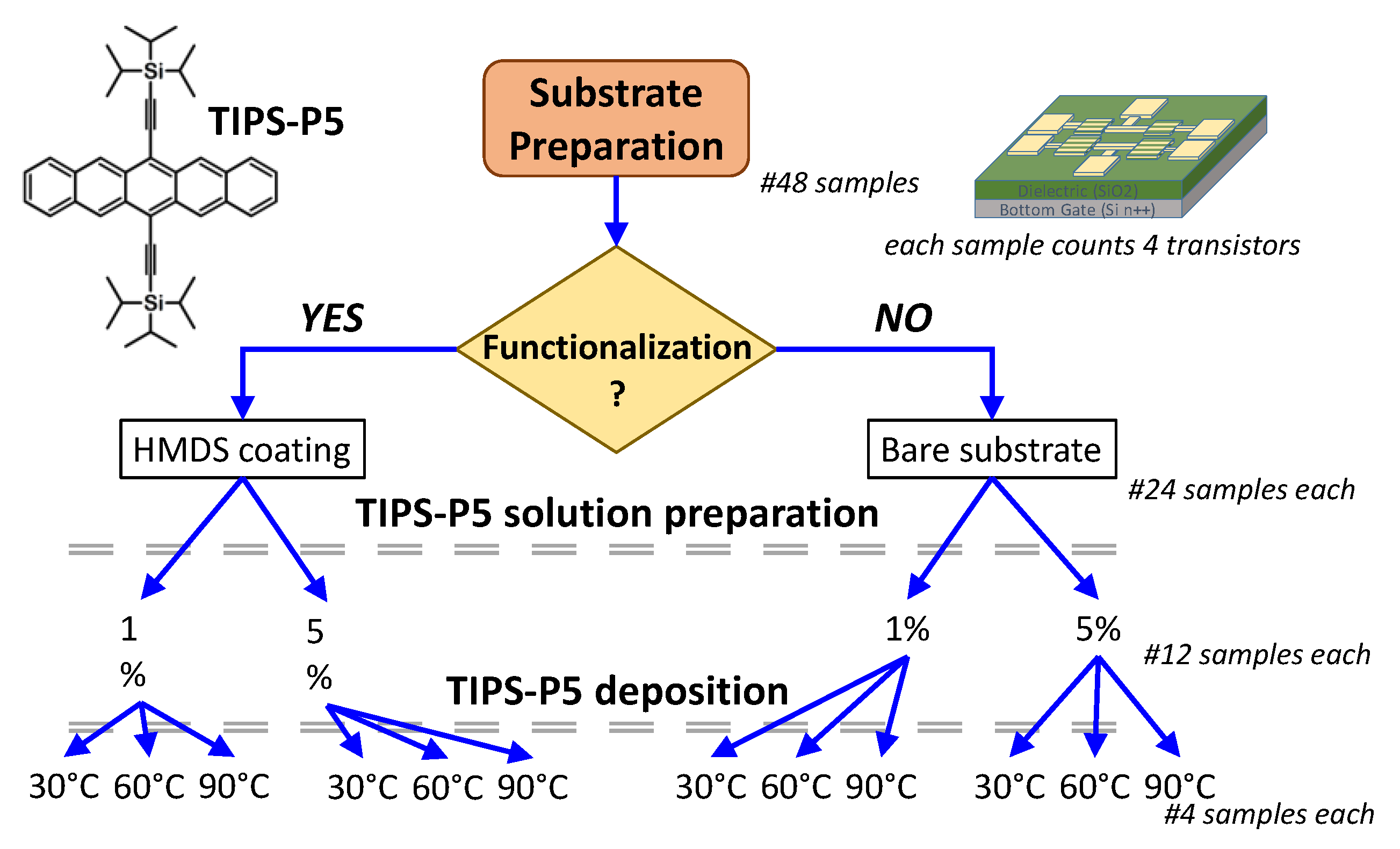
2.1. Devices Fabrication

BG-OFETs and TG-EGOFETs (depicted in Figure 1a,b, respectively) were fabricated onto the same Si/SiO2 substrates with interdigitated source and drain electrodes (purchased by Fondazione Bruno Kessler, Trento, Italy). In detail, 200 nm of SiO2 was thermally grown over a heavily doped n-type Si wafer forming the back-gate (n++ Si) and the back-gate dielectric (SiO2). Bottom contacts interdigitated source and drain gold electrodes with a thickness of 100–150 nm were obtained by photolithography above a chrome adhesion layer of 3–5 nm, defining the transistor channel with an aspect ratio Z = 560 (each substrate contains four transistors: two with channel length L = 20 µm and W = 11.2 mm, two with L = 40 µm and W = 22.4 mm). Finally, substrates were covered with a layer of photoresist to protect the gold electrodes during shipment.
As received, the substrates were cleaned in an ultrasonic bath with acetone to remove the protective layer of photoresist and other process residuals. A subsequent ultrasonic bath with isopropyl alcohol was done to remove any acetone residuals, promoting a less hydrophobic surface that allows for a better deposition of the semiconductor solution. After the cleaning procedure, half of the prepared substrates were treated with HMDS purchased from Sigma-Aldrich Chemical Co., St. Louis, MO, USA, whereas the other half were left untreated. The HMDS functionalization was performed by exposing the substrates for 2 h to HMDS vapor in a low vacuum chamber.
Two TIPS-P5 solutions (1% and 5% in weight) were prepared by dissolving the organic semiconductor using toluene as an organic solvent. Prior to the semiconductor deposition, the substrates were placed over a hot plate for about 15 min, allowing them to reach the preset deposition temperature (30 °C, 60 °C, and 90 °C). TIPS-P5 solution was drop-cast over each substrate (covering all four transistors in the sample) that was kept at the preset deposition temperature for about 15 min to promote the complete evaporation of the solvent. Before characterization, the samples were stored at room temperature in a nitrogen-saturated environment. High-resolution optical images of the deposed semiconductor are reported in Supplementary Figure S1 for the three deposition temperatures. In contrast, Supplementary Figure S2 shows contact angle measurement confirming the hydrophobicity of the semiconductor.
Notice that such fabrication protocol does not allow for fine control of the semiconductor deposition (thickness, morphology, and molecular ordering). However, thanks to the implementation of a double-layer architecture, BG-OFETs and TG-EGOFETs share the same semiconducting film. Therefore, performing electrical characterizations of the same device in both the BG and TG configurations ensures that performance differences between TG-EGOFETs and BG-OFETs in dependence on the HMDS functionalization are indeed due to the presence/absence of HMDS and not to the process variability.

2.2. Characterization Procedure

Electrical characterizations were performed in the dark inside a grounded Faraday cage using an Agilent B1500 parameter analyzer equipped with two high-power and two high-sensing source measurement units. The samples were initially characterized as standard BG-OFETs without putting the water drop on top of the semiconductor (no top gate). This allows us i) to avoid the capacitive coupling between the BG electronic channel and the TG electrode and ii) to perform a wider voltage scan (up to –20 V), avoiding any risk of electrolysis and preventing any damage to the organic semiconductor. Immediately after the BG measurements, the same transistors were characterized as TG-EGOFETs by using a MilliQ drop as gate medium and a 0.6 mm-thick platinum wire as the gate contact in Figure 1b.
For both BG-OFETs and TG-EGOFETs transfer (IDSVGS) and output (IDSVDS) double-sweep measurements were performed:
  • IDSVGS curves were taken by scanning VGS from +5 V to −20 V (with constant VDS = −1 V and −20 V) during BG-OFETs characterizations, whereas VGS was scanned from +0.1 V to −0.5 V (with constant VDS = −0.2 V and −0.5 V) during TG-EGOFETs characterizations.
  • IDSVDS curves were taken by scanning VDS from 0 V to −20 V (with constant VGS = −10 V and −20 V) during BG-OFETs characterizations, whereas VDS was scanned from 0 V to −0.5 V (with constant VGS = −0.2 V and −0.5 V) during TG-EGOFETs characterizations.
All the TG-EGOFETs measurements were performed by grounding the back-gate silicon electrode.

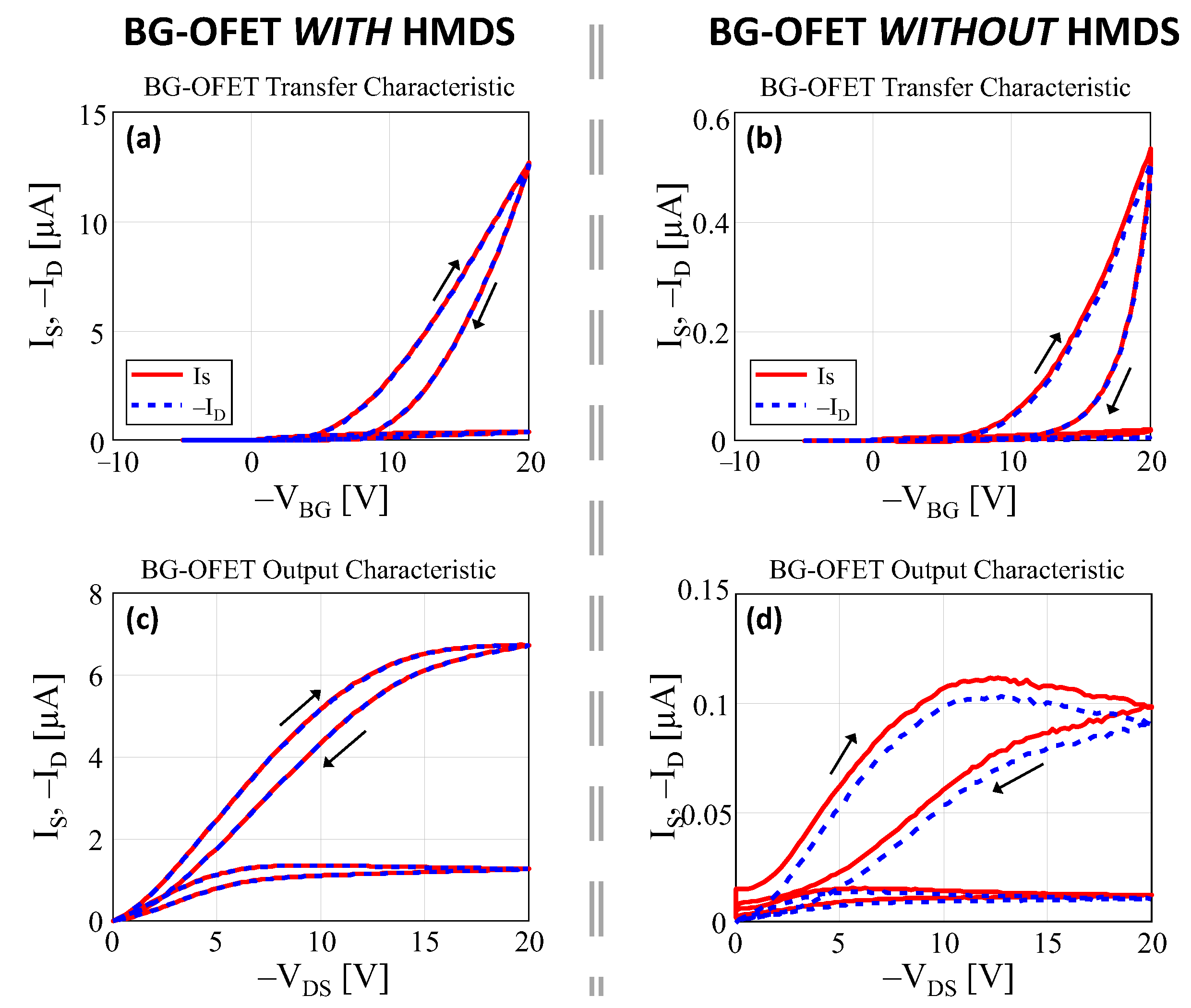
3. Results and Discussion

To investigate how the HMDS functionalization affects the performance of TIPS-P5 OFETs and EGOFETs, the samples were fabricated following the chart in Figure 2. In particular, we fabricated four samples for each deposition condition, and each sample contains four transistors (sixteen transistors for each case).
Figure 3 shows some representative OFET transfer and output characteristics (T = 90 °C and TIPS-P% solution = 1%) for HDMS treated and untreated samples. As can be seen from both transfer and output characteristics, BG-OFETs without HMDS feature small IDS currents and large clockwise hysteresis, which are an index of high molecular disorder and charge trapping at the SiO2/semiconductor interface [42]. OFETs fabricated using HMDS are characterized by higher currents and much smaller hysteresis, confirming that the use of HMDS for the fabrication of TIPS-P5-bases OFETs promotes a more favorable molecular arrangement for charge transport at the SiO2 interface.
In order to perform a direct comparison of the electrical characteristics of the fabricated devices, the mobility of the transistor μ F E T and threshold voltage V T were extrapolated from the saturation regime using the following equation:
I D S = 1 2 C G W L μ F E T V G S V T 2
with C G is the gate capacitance that is equal to 17 nF∙cm−2 for our BG transistors (200 nm-thick SiO2 dielectric). Note that Equation (1) is an approximated model that, in particular, neglects the increase of µ F E T with the overdrive voltage. Indeed, the literature reports several accurate models for charge transport in thin film and organic field-effect transistors [43,44,45]. However, more accurate models are characterized by more complex parameter extrapolation procedures that cannot always be applied due to the transistor’s non-ideality and non-stationary conditions. In this work, we chose to extrapolate the data using Equation (1) in order to allow good and reliable statistics to compare all the devices. However, when possible, we also implemented the more complex techniques cited above to check the validity of the data reported in this manuscript (as a reference, Supplementary Tables S1 and S2 report the BG-OFETs and TG-EGOFETs parameters extrapolated using the trans-conductance method).
The comparison of the extrapolated data, summarized in Table 1, clearly shows that OFETs fabricated using HMDS features higher field effect mobility, as expected. Furthermore, for both HMDS-treated and -untreated samples, the mobility increases by increasing the deposition temperature, suggesting that higher temperatures allow a more efficient molecule arrangement that improves the charge transport at the SiO2/TIPS-P5 interface. In addition, HMDS-treated devices show a reduction of the threshold voltage (in absolute value) with the increase in temperature. In contrast, no evident trend is observed in the threshold voltage of untreated devices. Hence, the combination of deposition temperature and HMDS functionalization can help in tuning the threshold voltage allowing the fabrication of devices for applications such as amplifiers and complementary logic gates, where the fine control of mobility and threshold voltage is of fundamental importance.
Right after the devices were characterized as standard BG-OFETs, a MilliQ drop was put directly on top of the semiconductor, as shown in Figure 1b, and the samples were characterized as TG-EGOFETs. EGOFETs working principle is very similar to OFETs, but instead of an insulator, it relies on the formation of an electrical double-layer as gate capacitance, thus allowing for very low top-gate voltages to drive the accumulation of carriers at the interface with the water (the reader may refer to [46] for a comprehensive review).
Representative transfer and output curves are reported in Figure 4, highlighting a quasi-hysteresis-free behavior typical of well-performing EGOFETs. Table 2 summaries the threshold voltage V T and field-effect mobility µ F E T estimated using Equation (1), where C G is now the double-layer capacitance that we estimated to be around 3.8 µF∙cm−2 by means of electrochemical impedance spectroscopy measurements [47]. Notably, the TG capacitance is much larger than the BG capacitance, allowing us to neglect the capacitive coupling between the Si BG electrode and the TG electronic channel of the EGOFETs [48].
Remarkably, TG-EGOFETs performance appears to have an opposite trend compared to BG-OFETs. Despite HMDS treatment having a beneficial effect on the BG transistors, it seems to impair EGOFETs performance. In fact, EGOFETs without HMDS treatment feature higher currents and higher mobilities than EGOFETs with HMDS treatment. Furthermore, increasing the deposition temperature no longer improves the performance of the device but, on the contrary, reduces the EGOFETs field-effect mobility. Notably, comparing TG-EGOFETs with BG-OFETs, we notice that devices fabricated without HMDS from 1% solution at 30 °C (i.e., best for EGOFETs performances) show larger TG mobilities than BG mobilities. This suggests that the charge transport is more favorable at the top semiconductor/liquid interface than at the bottom. Such a result is a further confirmation of the beneficial (almost mandatory) effects of HMDS in BG-OFETs, whereas it indicates that HMDS functionalization should be avoided when fabricating TIPS-P5-based EGOFETs.
Another important remark regarding EGOFETs threshold voltage is worth doing. EGOFETs without HMDS show an important positive threshold voltage shift compared with the threshold voltage of HMDS-treated EGOFETs. One might speculate that the introduction of the HMDS layer in the fabrication steps may introduce a different energy level alignment between the SiO2 dielectric and the semiconductor (via an interface dipole or by introducing/removing interface trap states). However, the same reasoning should also apply to BG-OFETs, which do not show a threshold voltage shift consistent with what is observed with the TG-EGOFETs. Therefore, we can rule out such a hypothesis. Tentatively, we could explain this threshold voltage shift as a consequence of different growth modalities of the semiconductor over the treated and untreated substrates. In fact, different molecule arrangements (orientation and grade of disorder) might lead to different semiconductor/liquid interfaces with an important impact on the threshold voltage during TG-EGOFET operation, but not during BG-OFET operation (which were characterized before putting the water on top). Furthermore, from contact angle measurements (Supplementary Figure S2), we observe that the EGOFETs with HMDS treatment feature larger contact angles than the EGOFETs fabricated without HMDS. Therefore, the EGOFETs with HMDS are more prone to repel water molecules; thus, higher gate voltages are required for charge accumulation, explaining both the positive threshold voltage shift and the higher field-effect mobility of EGOFETs without HMDS.
Finally, we cannot rule out the possibility of device degradation during the characterization protocol. In fact, in previous work, we showed that the TIPS-P5 EGOFETs (without HMDS) features an initial positive threshold voltage shift during stress [16]. Note that the voltage shift reported in [16] becomes appreciable after several hours of stress, which is not the case with our characterization protocol, which lasts only a few minutes. The entity of such variation could depend on the stress/characterization protocol and the morphological structure of the semiconductor layer, and it may be the subject of future studies.

4. Conclusions

In this work, we fabricated transistors using a double-gate architecture as a versatile platform to study the transport properties of a material in the BG and TG transistor architecture. In particular, we investigated how the HMDS treatment of Si/SiO2 substrates impacts the TIPS-P5 EGOFETs performance, showing that, as opposed to BG-OFETs, the HMDS functionalization negatively affects EGOFETs performance by reducing the carriers’ mobility. Our approach allows a direct comparison of the TG and BG performances of the devices independently, particularly on the film morphology and structure characteristics. This is ideal to compensate for the variability of the solution processing and can be used as a general platform for a self-consistent characterization of amorphous thin-film semiconductors. Among the investigated fabrication parameters, the substrate treatment shows the largest impact on both OFETs and EGOFETs performance, followed by a dependence of the estimated figures of merit with the deposition temperature. Conversely, the comparison of the solution concentration shows how both the BG and TG devices, either with or without HMDS treatment, share similar behaviors. This points to the fact that a low (1%) TIPS-P5 concentration is favorable for device fabrication since it enables OFETs and EGOFETs with higher field-effect mobility than devices fabricated using a high (5%) concentration.
Considering the HMDS treatment instead, we can conclude that achieving high-performing TIPS-P5-based BG transistors on Si/SiO2 substrates means HMDS treatment should be a mandatory step in the fabrication process. Moreover, the deposition temperature should be carefully selected to improve the field-effect mobility and tune the transistor threshold voltage to get the desired value. Conversely, the opposite observations can be taken for the TG-EGOFETs, for which the HMDS treatment should be avoided. Furthermore, the deposition temperature should be trimmed to match the complete evaporation of the solvent (which is favored at high temperatures) and to ensure good field-effect performances (which may be degraded by an excessively high deposition temperature).
We believe that this work provides useful hints for the fabrication of TIPS-P5 devices, not only for the drop-casting process over standard Si/SiO2 substrates but also for emerging flexible ink-jet printing technologies. Indeed, during the printing process, substrate choice and functionalization are critical steps to ensure material deposition and adhesion. At the same time, reducing the number and complexity of the fabrication processes is the key to low-cost and fully printed electronics.

Supplementary Materials

The following supporting information can be downloaded at: https://www.mdpi.com/article/10.3390/electronicmat3040024/s1, Figure S1: TIPS-P5 optical images; Figure S2: Contact angle measurements; Figure S3: BG-leakage currents; Figure S4: TG-leakage currents; Table S1: BG-OFETs additional parameters; Table S2: TG-EGOFETs additional parameters.

Author Contributions

Conceptualization, N.L. and M.B.; methodology, M.B. and F.P.; validation, N.L. and M.B.; formal analysis, N.L.; investigation, N.L. and M.B.; resources, S.T. and M.M.; data curation, N.L. and M.B.; writing—original draft preparation, N.L.; writing—review and editing, N.L., M.B., F.P., S.T., M.M. and. A.C.; visualization, N.L.; supervision, S.T. and A.C.; project administration, A.C.; funding acquisition, A.C. All authors have read and agreed to the published version of the manuscript.

Funding

This work was partially supported by the University of Padova, Department of Information Engineering, under the initiative Project PROACTIVE 2018, and by MIUR (Italian Minister for Education) under the initiative “Departments of Excellence” (Law 232/2016).

Institutional Review Board Statement

Not applicable.

Informed Consent Statement

Not applicable.

Data Availability Statement

The data that support the findings of this study are available on request from the corresponding author.

Conflicts of Interest

The authors declare no conflict of interest.

References

  1. Muccini, M.; Toffanin, S. Organic Light-Emitting Transistors: Towards the Next Generation Display Technology; A Wiley-Science Wise Co-Publication; John Wiley & Sons: Hoboken, NJ, USA, 2016; ISBN 978-1-118-10007-3. [Google Scholar]
  2. Gomes, A.; Priyadarshana, L.L.; Visser, A.; Carrascal, J.P.; Vertegaal, R. Magicscroll: A Rollable Display Device with Flexible Screen Real Estate and Gestural Input. In Proceedings of the 20th International Conference on Human-Computer Interaction with Mobile Devices and Services, Barcelona, Spain, 3–6 September 2018; ACM: New York, NY, USA, 2018; Volume 6, pp. 1–11. [Google Scholar]
  3. Koo, J.H.; Kim, D.C.; Shim, H.J.; Kim, T.-H.; Kim, D.-H. Flexible and Stretchable Smart Display: Materials, Fabrication, Device Design, and System Integration. Adv. Funct. Mater. 2018, 28, 1801834. [Google Scholar] [CrossRef]
  4. Wu, W.-J.; Chen, J.-W.; Wang, J.-S.; Zhou, L.; Tao, H.; Zou, J.-H.; Xu, M.; Wang, L.; Peng, J.-B.; Chan, M. High-Resolution Flexible AMOLED Display Integrating Gate Driver by Metal–Oxide TFTs. IEEE Electron Device Lett. 2018, 39, 1660–1663. [Google Scholar] [CrossRef]
  5. Gao, W.; Ota, H.; Kiriya, D.; Takei, K.; Javey, A. Flexible Electronics toward Wearable Sensing. Acc. Chem. Res. 2019, 52, 523–533. [Google Scholar] [CrossRef] [PubMed]
  6. Yin, D.; Chen, Z.-Y.; Jiang, N.-R.; Liu, Y.-F.; Bi, Y.-G.; Zhang, X.-L.; Han, W.; Feng, J.; Sun, H.-B. Highly Transparent and Flexible Fabric-Based Organic Light Emitting Devices for Unnoticeable Wearable Displays. Org. Electron. 2020, 76, 105494. [Google Scholar] [CrossRef]
  7. Lv, J.; Zhou, P.; Zhang, L.; Zhong, Y.; Sui, X.; Wang, B.; Chen, Z.; Xu, H.; Mao, Z. High-Performance Textile Electrodes for Wearable Electronics Obtained by an Improved in Situ Polymerization Method. Chem. Eng. J. 2019, 361, 897–907. [Google Scholar] [CrossRef]
  8. Lin, P.; Yan, F. Organic Thin-Film Transistors for Chemical and Biological Sensing. Adv. Mater. 2012, 24, 34–51. [Google Scholar] [CrossRef]
  9. Benfenati, V.; Toffanin, S.; Bonetti, S.; Turatti, G.; Pistone, A.; Chiappalone, M.; Sagnella, A.; Stefani, A.; Generali, G.; Ruani, G.; et al. A Transparent Organic Transistor Structure for Bidirectional Stimulation and Recording of Primary Neurons. Nat. Mater. 2013, 12, 672–680. [Google Scholar] [CrossRef] [PubMed]
  10. Lago, N.; Cester, A. Flexible and Organic Neural Interfaces: A Review. Appl. Sci. 2017, 7, 1292. [Google Scholar] [CrossRef]
  11. Kubota, R.; Sasaki, Y.; Minamiki, T.; Minami, T. Chemical Sensing Platforms Based on Organic Thin-Film Transistors Functionalized with Artificial Receptors. ACS Sens. 2019, 4, 2571–2587. [Google Scholar] [CrossRef]
  12. Kuribara, K.; Hori, Y.; Katashita, T.; Kakita, K.; Tanaka, Y.; Yoshida, M. Organic Physically Unclonable Function on Flexible Substrate Operable at 2 V for IoT/IoE Security Applications. Org. Electron. 2017, 51, 137–141. [Google Scholar] [CrossRef]
  13. Zeb, S.; Habib, A.; Amin, Y.; Tenhunen, H.; Loo, J. Green Electronic Based Chipless Humidity Sensor for IoT Applications. In Proceedings of the 2018 IEEE Green Technologies Conference (GreenTech), Austin, TX, USA, 4–6 April 2018; pp. 172–175. [Google Scholar]
  14. Jo, I.Y.; Park, J.-G.; Moon, J.-H.; Jung, J.Y.; Kim, D.E.; Baeg, K.-J. Low-Voltage-Operating Complementary-like Circuits Using Ambipolar Organic-Inorganic Hybrid Thin-Film Transistors with Solid-State-Electrolyte Gate Insulator. Org. Electron. 2019, 75, 105358. [Google Scholar] [CrossRef]
  15. Cho, S.Y.; Ko, J.M.; Lim, J.; Lee, J.Y.; Lee, C. Inkjet-Printed Organic Thin Film Transistors Based on TIPS Pentacene with Insulating Polymers. J. Mater. Chem. C 2013, 1, 914–923. [Google Scholar] [CrossRef]
  16. Lago, N.; Buonomo, M.; Imran, S.; Bertani, R.; Wrachien, N.; Bortolozzi, M.; Pedersen, M.G.; Cester, A. TIPS-Pentacene as Biocompatible Material for Solution Processed High-Performance Electronics Operating in Water. IEEE Electron Device Lett. 2018, 39, 1401–1404. [Google Scholar] [CrossRef]
  17. Park, S.K.; Jackson, T.N.; Anthony, J.E.; Mourey, D.A. High Mobility Solution Processed 6,13-Bis(Triisopropyl-Silylethynyl) Pentacene Organic Thin Film Transistors. Appl. Phys. Lett. 2007, 91, 063514. [Google Scholar] [CrossRef]
  18. Zhang, Q.; Leonardi, F.; Casalini, S.; Temiño, I.; Mas-Torrent, M. High Performing Solution-Coated Electrolyte-Gated Organic Field-Effect Transistors for Aqueous Media Operation. Sci. Rep. 2016, 6, 39623. [Google Scholar] [CrossRef]
  19. Zhang, Q.; Leonardi, F.; Casalini, S.; Mas-Torrent, M. Mercury-Mediated Organic Semiconductor Surface Doping Monitored by Electrolyte-Gated Field-Effect Transistors. Adv. Funct. Mater. 2017, 27, 1703899. [Google Scholar] [CrossRef]
  20. Lago, N.; Wrachien, N.; Pedersen, M.G.; Cester, A. Simultaneous Stimulation and Recording of Cell Activity with Reference-Less Sensors: Is It Feasible? Org. Electron. 2018, 62, 676–684. [Google Scholar] [CrossRef]
  21. Buonomo, M.; Lago, N. Self-Polarization in Reference-Less Electrolyte-Gated Organic Field-Effect Transistors. IEEE Electron Device Lett. 2020, 41, 477–480. [Google Scholar] [CrossRef]
  22. Picca, R.A.; Manoli, K.; Macchia, E.; Sarcina, L.; Franco, C.D.; Cioffi, N.; Blasi, D.; Österbacka, R.; Torricelli, F.; Scamarcio, G.; et al. Ultimately Sensitive Organic Bioelectronic Transistor Sensors by Materials and Device Structure Design. Ads. Funct. Mater. 2019, 30, 1904513. [Google Scholar] [CrossRef]
  23. Piro, B.; Mattana, G.; Reisberg, S. Transistors for Chemical Monitoring of Living Cells. Biosensors 2018, 8, 65. [Google Scholar] [CrossRef] [Green Version]
  24. Kim, S.H.; Lee, J.; Park, N.; Min, H.; Park, H.W.; Kim, D.H.; Lee, H.S. Impact of Energetically Engineered Dielectrics on Charge Transport in Vacuum-Deposited Bis(Triisopropylsilylethynyl)Pentacene. J. Phys. Chem. C 2015, 119, 28819–28827. [Google Scholar] [CrossRef]
  25. Wang, Z.; Huang, L.; Zhu, X.; Zhou, X.; Chi, L. An Ultrasensitive Organic Semiconductor NO2 Sensor Based on Crystalline TIPS-Pentacene Films. Adv. Mater. 2017, 29, 1703192. [Google Scholar] [CrossRef] [PubMed]
  26. Lee, W.H.; Kim, D.H.; Jang, Y.; Cho, J.H.; Hwang, M.; Park, Y.D.; Kim, Y.H.; Han, J.I.; Cho, K. Solution-Processable Pentacene Microcrystal Arrays for High Performance Organic Field-Effect Transistors. Appl. Phys. Lett. 2007, 90, 132106. [Google Scholar] [CrossRef]
  27. Cosseddu, P.; Lai, S.; Barbaro, M.; Bonfiglio, A. Ultra-Low Voltage, Organic Thin Film Transistors Fabricated on Plastic Substrates by a Highly Reproducible Process. Appl. Phys. Lett. 2012, 100, 093305. [Google Scholar] [CrossRef]
  28. Zhao, X.; Zhang, B.; Tang, Q.; Ding, X.; Wang, S.; Zhou, Y.; Tong, Y.; Liu, Y. Conformal Transistor Arrays Based on Solution-Processed Organic Crystals. Sci. Rep. 2017, 7, 15367. [Google Scholar] [CrossRef]
  29. Ohe, T.; Kuribayashi, M.; Yasuda, R.; Tsuboi, A.; Nomoto, K.; Satori, K.; Itabashi, M.; Kasahara, J. Solution-Processed Organic Thin-Film Transistors with Vertical Nanophase Separation. Appl. Phys. Lett. 2008, 93, 053303. [Google Scholar] [CrossRef]
  30. Li, X.; Kim, K.; Oh, H.; Moon, H.C.; Nam, S.; Kim, S.H. Cone-Jet Printing of Aligned Silver Nanowire/Poly(Ethylene Oxide) Composite Electrodes for Organic Thin-Film Transistors. Org. Electron. 2019, 69, 190–199. [Google Scholar] [CrossRef]
  31. Jain, S.; Surya, S.G.; Suggisetti, P.K.; Gupta, A.; Rao, V.R. Sensitivity Improvement of Medical Dosimeters Using Solution Processed TIPS-Pentacene FETs. IEEE Sens. J. 2019, 19, 4428–4434. [Google Scholar] [CrossRef]
  32. Park, B.; Bae, I.-G.; Kwon, O.E.; Jeon, H.G. Organic Thin-Film Transistors Fabricated Using a Slot-Die-Coating Process and Related Sensing Applications. RSC Adv. 2016, 6, 101613–101621. [Google Scholar] [CrossRef]
  33. Da Rocha, C.T.; Haase, K.; Zheng, Y.; Löffler, M.; Hambsch, M.; Mannsfeld, S.C.B. Solution Coating of Small Molecule/Polymer Blends Enabling Ultralow Voltage and High-Mobility Organic Transistors. Adv. Electron. Mater. 2018, 4, 1800141. [Google Scholar] [CrossRef]
  34. Lin, Z.; Guo, X.; Zhou, L.; Zhang, C.; Chang, J.; Wu, J.; Zhang, J. Solution-Processed High Performance Organic Thin Film Transistors Enabled by Roll-to-Roll Slot Die Coating Technique. Org. Electron. 2018, 54, 80–88. [Google Scholar] [CrossRef]
  35. Mattana, G.; Loi, A.; Woytasik, M.; Barbaro, M.; Noël, V.; Piro, B. Inkjet-Printing: A New Fabrication Technology for Organic Transistors. Adv. Mater. Technol. 2017, 2, 1700063. [Google Scholar] [CrossRef]
  36. Raghuwanshi, V.; Bharti, D.; Mahato, A.K.; Varun, I.; Tiwari, S.P. Solution-Processed Organic Field-Effect Transistors with High Performance and Stability on Paper Substrates. ACS Appl. Mater. Interfaces 2019, 11, 8357–8364. [Google Scholar] [CrossRef]
  37. Lago, N.; Buonomo, M.; Molina, G.R.; Pollesel, A.; Hensel, R.C.; Sedona, F.; Sambi, M.; Torrent, M.M.; Casalini, S.; Cester, A. Real-time threshold voltage compensation on dual-gate electrolyte-gated organic field-effect transistors. Org. Electron. 2022, 106, 106531. [Google Scholar] [CrossRef]
  38. Zhang, Y.; Li, J.; Sbircea, D.T.; Giovannitti, A.; Xu, J.; Xu, H.; Zhou, G.; Bian, L.; McCulloch, I.; Zhao, N. Liquid–Solid Dual-Gate Organic Transistors with Tunable Threshold Voltage for Cell Sensing. ACS Appl. Mater. Interfaces 2017, 9, 38687–38694. [Google Scholar] [CrossRef]
  39. Devynck, M.; Tardy, P.; Wantz, G.; Nicolas, Y.; Hirsch, L. Organic Field-Effect Transistor with Octadecyltrichlorosilane (OTS) Self-Assembled Monolayers on Gate Oxide: Effect of OTS Quality. Eur. Phys. J. Appl. Phys. 2011, 56, 34106. [Google Scholar] [CrossRef]
  40. Sista, P.; Bhatt, M.P.; Mccary, A.R.; Nguyen, H.; Hao, J.; Biewer, M.C.; Stefan, M.C. Enhancement of OFET Performance of Semiconducting Polymers Containing Benzodithiophene upon Surface Treatment with Organic Silanes. J. Polym. Sci. Part A Polym. Chem. 2011, 49, 2292–2302. [Google Scholar] [CrossRef]
  41. Smith, J.W.H.; Hill, I.G. Influence of SiO2 Dielectric Preparation on Interfacial Trap Density in Pentacene-Based Organic Thin-Film Transistors. J. Appl. Phys. 2007, 101, 044503. [Google Scholar] [CrossRef]
  42. Sirringhaus, H. Reliability of Organic Field-Effect Transistors. Adv. Mater. 2009, 21, 3859–3873. [Google Scholar] [CrossRef]
  43. Servati, P.; Striakhilev, D.; Nathan, A. Above-Threshold Parameter Extraction and Modeling for Amorphous Silicon Thin-Film Transistors. IEEE Trans. Electron Devices 2003, 50, 2227–2235. [Google Scholar] [CrossRef]
  44. Tu, D.; Herlogsson, L.; Kergoat, L.; Crispin, X.; Berggren, M.; Forchheimer, R. A Static Model for Electrolyte-Gated Organic Field-Effect Transistors. IEEE Trans. Electron Devices 2011, 58, 3574–3582. [Google Scholar] [CrossRef]
  45. Buonomo, M.; Lago, N.; Cantarella, G.; Wrachien, N.; Natali, M.; Prescimone, F.; Benvenuti, E.; Muccini, M.; Toffanin, S.; Cester, A. Simple and Accurate Single Transistor Technique for Parameters Extraction from Organic and Inorganic Thin Film Devices. Org. Electron. 2018, 63, 376–383. [Google Scholar] [CrossRef]
  46. Kergoat, L.; Piro, B.; Berggrer, M.; Horowitz, G.; Pham, M.C. Advances in organic transistor-based biosensors: From organic electrochemical transistors to electrolyte-gated organic field-effect transistors. Anal. Bioanal. Chem. 2012, 402, 1813–1826. [Google Scholar] [CrossRef] [PubMed]
  47. Lago, N.; Buonomo, M.; Wrachien, N.; Prescimone, F.; Natali, M.; Muccini, M.; Toffanin, S.; Cester, A. A General Equivalent Circuit Model for a Metal/Organic/Liquid/Metal System. IEEE Trans. Electron Devices 2018, 65, 4555–4562. [Google Scholar] [CrossRef]
  48. Colinge, J.-P. Silicon-on-Insulator Technology: Materials to VLSI: Materials to VLSI, 3rd ed.; Springer: New York, NY, USA, 2004; ISBN 978-1-4020-7773-9. [Google Scholar]
Figure 1. Graphical representation of the BG-OFETs (a) and TG-EGOFETs (b) architectures.
Electronicmat 03 00024 g001
Figure 2. Flowchart of the devices’ fabrication procedure.
Electronicmat 03 00024 g002
Figure 3. BG-OFETs characterizations with and without HMDS functionalization: (a) Transfer characteristics with HMDS; (b) transfer characteristics without HMDS; (c) output characteristics with HMDS; (d) output characteristics without HMDS. Discrepancies between the source (IS) and drain (ID) currents are due to BG leakage current (see Supplementary Figure S3).
Electronicmat 03 00024 g003
Figure 4. TG-EGOFETs characterizations with and without HMDS functionalization: (a) Transfer characteristics with HMDS; (b) transfer characteristics without HMDS; (c) output characteristics with HMDS; (d) output characteristics without HMDS. Discrepancies between the source (IS) and drain (ID) currents are due to the TG leakage current (see Supplementary Figure S4).
Electronicmat 03 00024 g004
Table 1. BG-OFETs parameters extrapolated using Equation (1). All the reported values are averaged over 16 transistors.
TIPS-P5 SolutionDeposition Temperature (°C)With HMDS FunctionalizationWithout HMDS Functionalization
Mobility
(cm2 V−1 s−1)
Threshold Voltage (V)Mobility
(cm2 V−1 s−1)
Threshold Voltage (V)
1%301.62 × 10⁻³−8.375.17 × 10−4−6.98
602.44 × 10⁻³−5.957.15 × 10−4−6.29
903.86 × 10⁻³−4.681.16 × 10−3−6.44
5%301.35 × 10⁻³−6.352.60 × 10−4−3.22
601.34 × 10⁻³−2.724.19 × 10−4−6.24
902.70 × 10⁻³−3.071.17 × 10−3−5.21
Table 2. TG-OFETs parameters extrapolated using Equation (1). All the reported values are averaged over 16 transistors.
TIPS-P5 SolutionDeposition Temperature (°C)With HMDS FunctionalizationWithout HMDS Functionalization
Mobility
(cm2 V−1 s−1)
Threshold Voltage (mV)Mobility
(cm2 V−1 s−1)
Threshold Voltage (mV)
1%304.42 × 10⁻⁴−136.991.15 × 10−356.99
601.41 × 10⁻⁴−15.177.23 × 10−426.19
901.39 × 10⁻⁴−19.884.55 × 10−4−3.75
5%301.63 × 10⁻⁴−54.181.53 × 10−475.94
602.81 × 10−5146.364.91 × 10−4128.08
903.08 × 10−5102.572.19 × 10−496.50
Publisher’s Note: MDPI stays neutral with regard to jurisdictional claims in published maps and institutional affiliations.

