1. Introduction
Silicon (Si) power devices have dominated the world of power electronics in recent years, and they have proven to be efficient in a wide range of applications. However, high-power, high-frequency, and high-temperature applications require more than Si can deliver. Wide band-gap (WBG) devices such as silicon carbide (SiC) MOSFETs have been intensively researched and developed for power electronics applications due to the substantial advantages their inherent material properties could realize at device level, such as high breakdown voltage, high operating electric field, high operating temperature, high switching frequency, and low losses [
1,
2,
3].
Commercial SiC-MOSFETs (1.7 kV, 3.3 kV and 10 kV) have attracted great attention, especially for medium-high voltage applications under higher switching frequencies [
4,
5]. To further increase the device blocking voltage level, high and medium voltage switching devices by connecting SiC-MOSFETs in series connection is desired since series-connected devices are an effective way to increase the blocking voltage capabilities of the SiC-based switches to answer application constraints above 1.7 kV. Furthermore, according to [
6], using two or more medium-voltage semiconductors in series features better on-resistance and higher current density than using a single higher-voltage device. However, the main problem related to the series association of power devices is the unequal voltage sharing among them that, if not mitigated, can result in device failure.
The voltage balancing across the series-connected devices is mainly caused by the tolerance in device parameters, package/layout parasitic components, and gate signal timing delays [
7,
8,
9]. Careful selection of power semiconductor devices, which have parameters with low spread and synchronizing gate-drive signals, are helpful in reducing voltages unbalance across the power devices. In addition to this, snubber circuits, active gate drive circuits, voltage clamping techniques [
7,
8,
9,
10,
11], and new concepts of packaging as described in [
12,
13] have also been reported as interesting contributions in an attempt to reduce or even remove the voltage unbalance among the series-connected power devices.
Considering the high switching speed behavior of SiC-MOSFETs, intrinsic device parasitic and external parasitic capacitances have a strong impact on the dynamic voltage-sharing performance. As demonstrated in [
13], one of the most important parasitic capacitances contributing to unequal dynamic voltage sharing among series-connected devices is the parasitic capacitance introduced by the packaging (
Cpac), which is located between the drain terminal of the device and the common baseplate of the power module or common heatsink.
Parasitic capacitances introduced by the gate driver circuitry can also impact the voltage-sharing performance [
3,
14]. However, in order to focus on the impact of the packaging/layout on the dynamic voltage sharing without having to consider the impact of the gate drivers and theirs supplies, their influence is neglected in this paper. In the experiments, batteries are used to supply the gate drivers, and optical fibers are used to transfer the gate signals. A circuit is implemented in each gate driver to adjust the delay time among them and to tune the switching transitions. In such a way, and if enough care is carried out for the implementation, gate driver circuitry impacts on the voltage unbalancing can be neglected.
The paper is organized as follows: In
Section 2, the traditional packaging is presented, and an analytical modeling is proposed. The influence of the packaging parasitic capacitance on voltage balancing is analyzed; in
Section 3, the proposed multi-step package (MSP) concept is presented, where a new package geometry is investigated to reconfigure the packaging parasitic capacitance network. A sensitive analysis is used to estimate the impacts of the delay between gate signals and device parameter mismatch on the proposed MSP. The experimental analyses of the classical planar and MSP are presented in
Section 4. In
Section 5, a brief thermal management discussion is presented in order to clarify the MSP limitations and indicate the ways to optimize the MSP from a thermal point of view.
2. Impact of Traditional Planar Packaging Parasitic Capacitances on Voltage Balancing
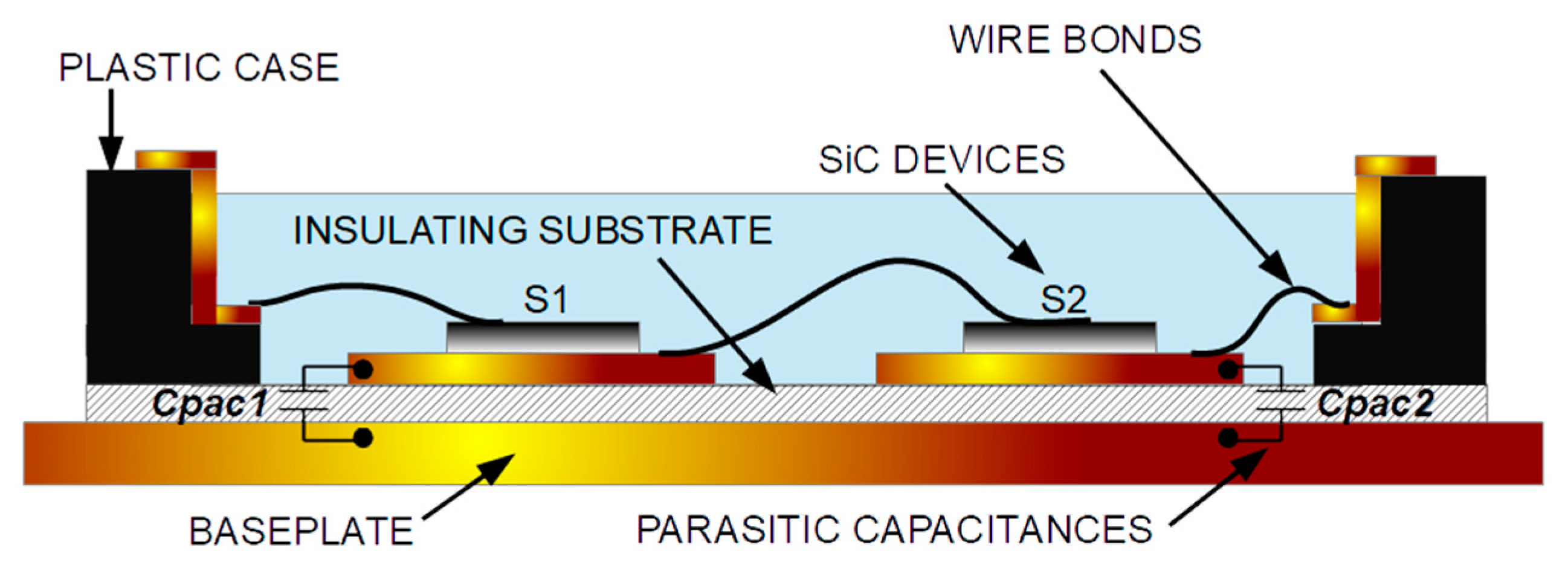
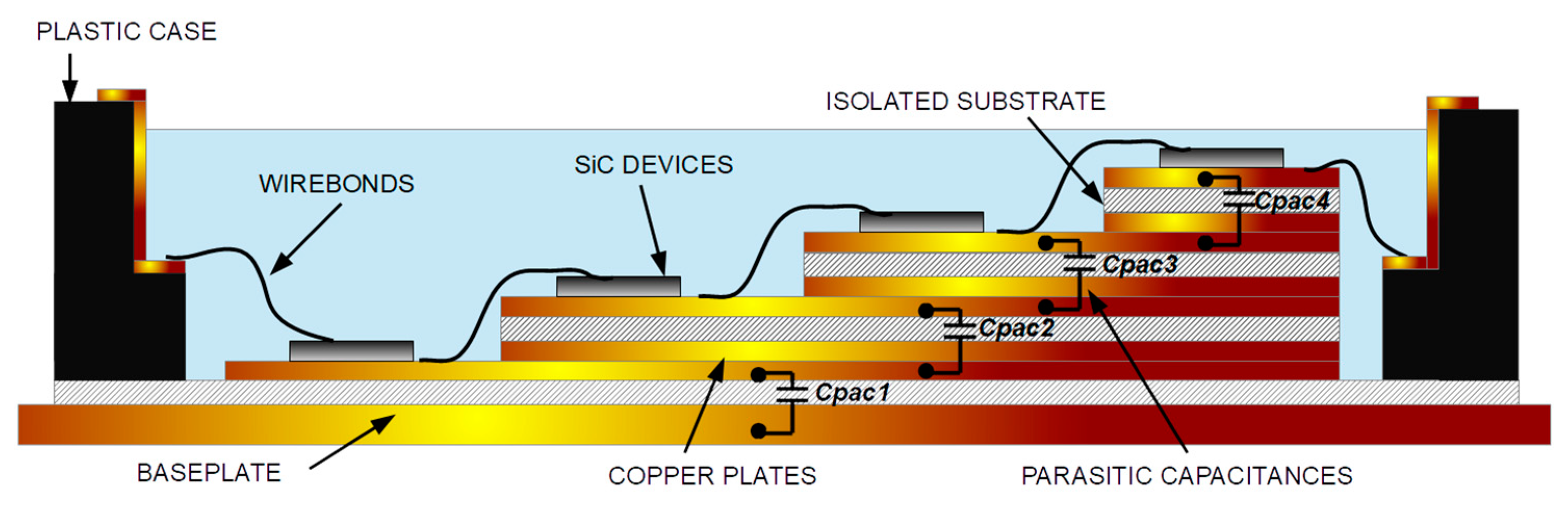
To analyze the influence of parasitic capacitances introduced by the classical packaging/layout, a cross-section of a simplified planar package and its main elements are shown in
Figure 1, which includes a base-plate, a Direct Bonded Copper (DBC) substrate, and two vertical series-connected SiC-MOSFETs.
In terms of voltage balancing and switching speed performances, the drain-attached copper trace to ground parasitic capacitances (
Cpac) introduced by the packaging is critical. This parasitic capacitance is a key point in the voltage balancing analysis performed in this work. In
Figure 1, two series-connected devices are considered in a traditional planar package. Therefore, two parasitic capacitances (
Cpac1 and
Cpac2) are introduced, which represent the modelling of the copper traces attached to the drain in front of the baseplate.
To analyze the influence of the parasitic capacitances
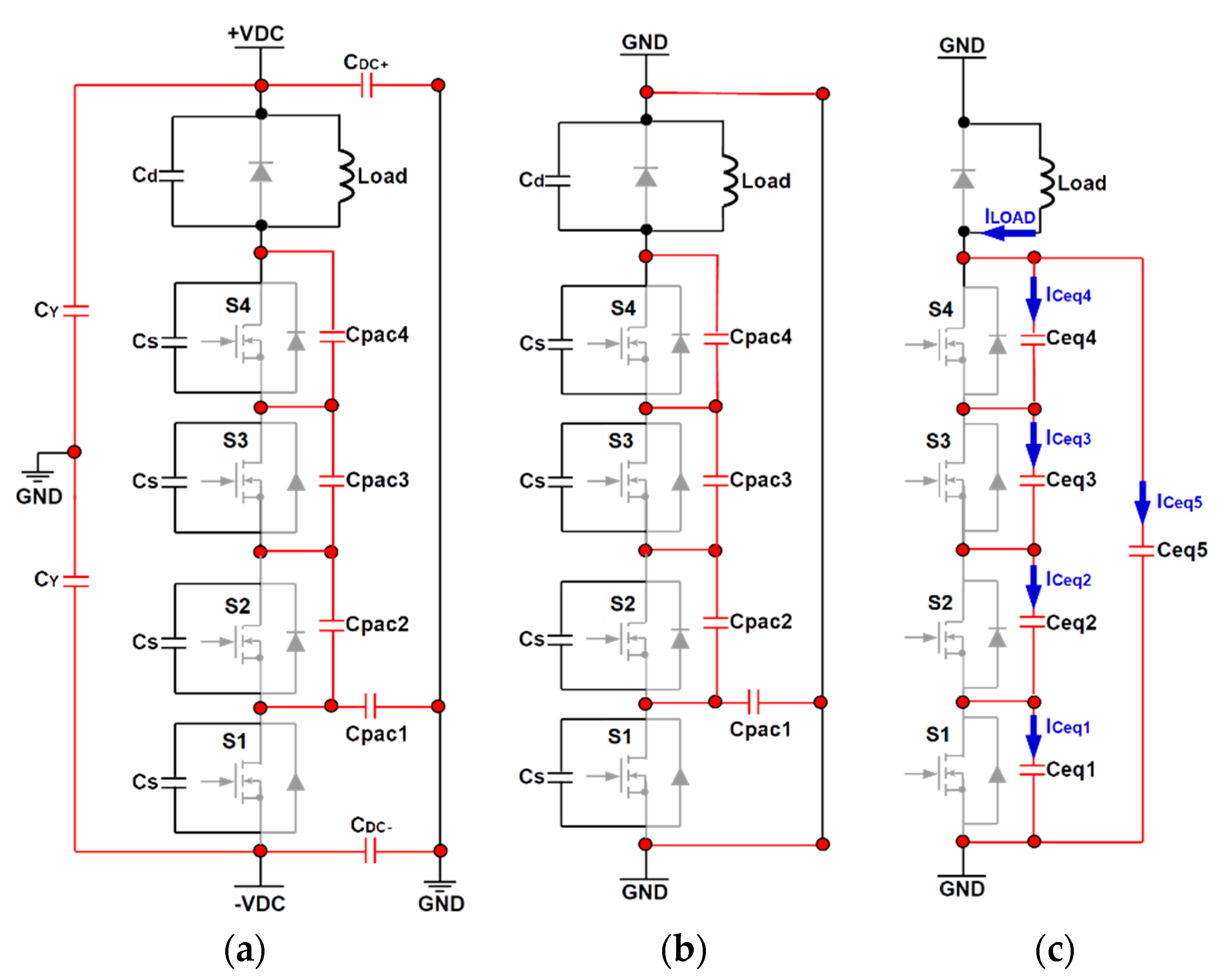
Cpac on the dynamic voltage unbalancing and on the switching speed behavior of the switching cell, an electrical scheme of four SiC-MOSFETs connected in series is considered and shown in
Figure 2. Where
Cpac1,
Cpac2,
Cpac3, and
Cpac4 are the drain-to-heatsink parasitic capacitances introduced by the packaging. C
DC+ and C
DC− are the parasitic capacitances from the DC bus to the ground. During the switching events, large current spikes flow from the floating potential nodes to the ground through the heatsink. These currents cause EMI issues, which limit the switching speed of the circuit [
15,
16]. In [
17], the use of Y-capacitors (
CY) is suggested to suppress this EMI.
CY are usually placed between +VDC and GND, and −VDC and GND. It is important to note that, for security reasons, the heatsink is attached to the reference potential of the remote-control circuit (GND), not to −VDC.
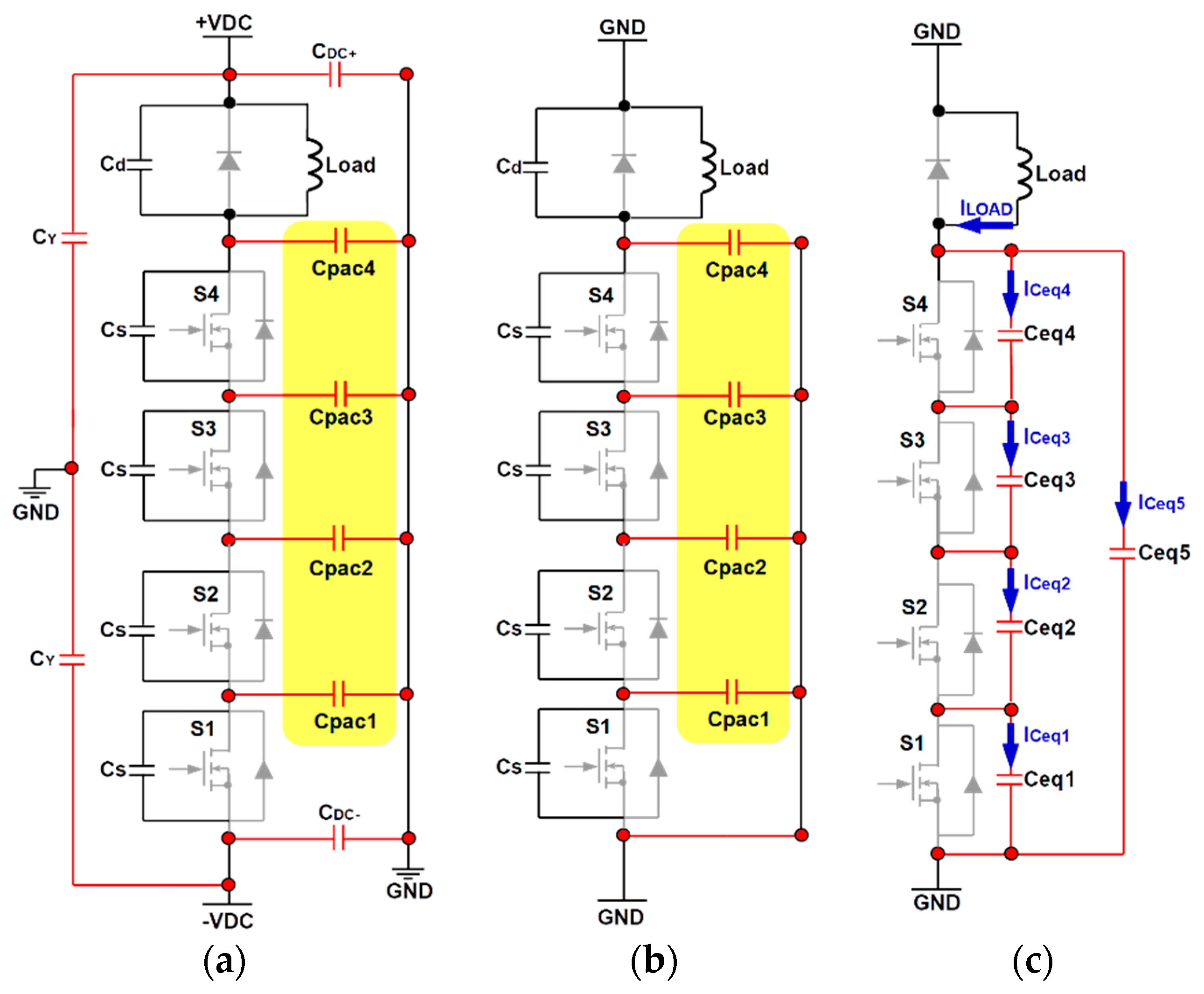
The capacitors
Cpac1,
Cpac2,
Cpac3, and
Cpac4 shown in
Figure 2 are roughly all the same. However, the
dv/dt applied to each of them is different with respect to the position of the device in the stack. Therefore, each parasitic capacitor carries a parasitic current that is getting greater and greater with the device number in the stack (starting from the bottom). The capacitors that generate these currents can be estimated based on the planar capacitance Equation (1).
where
is the absolute permittivity of the isolated substrate,
is the area of the copper trace on which the SiC device is attached, and
is the distance between the copper plate and the baseplate.
Considering that all SiC-MOSFETs in
Figure 2 are identical, and
Cpac1 =
Cpac2 =
Cpac3 =
Cpac4 =
Cpac,
Figure 2 can be redrawn as shown in
Figure 3a, where
Cd is the intrinsic parasitic capacitance of the diode, and
CS is the intrinsic equivalent parasitic capacitance of each SiC-MOSFET, which is expressed by Equation (2). In the following analyses, it is supposed that the series-connected SiC-MOSFETs are turning off, and the drain-to-source voltages of the series-connected devices are starting to rise. In other words, the device gate-to-source voltages are under the Miller Plateau region.
As shown in
Figure 3b, a high-frequency equivalent circuit can be simplified by short-circuiting the DC-bus terminals and CY capacitors. Redrawing
Figure 3b, a further simplified high-frequency equivalent scheme can be achieved as shown in
Figure 3c, where
Ceq1,
Ceq2,
Ceq3, and
Ceq4 are, respectively, the equivalent drain-to-source capacitances of devices S1, S2, S3, and S4, which are expressed by Equations (3)–(7).
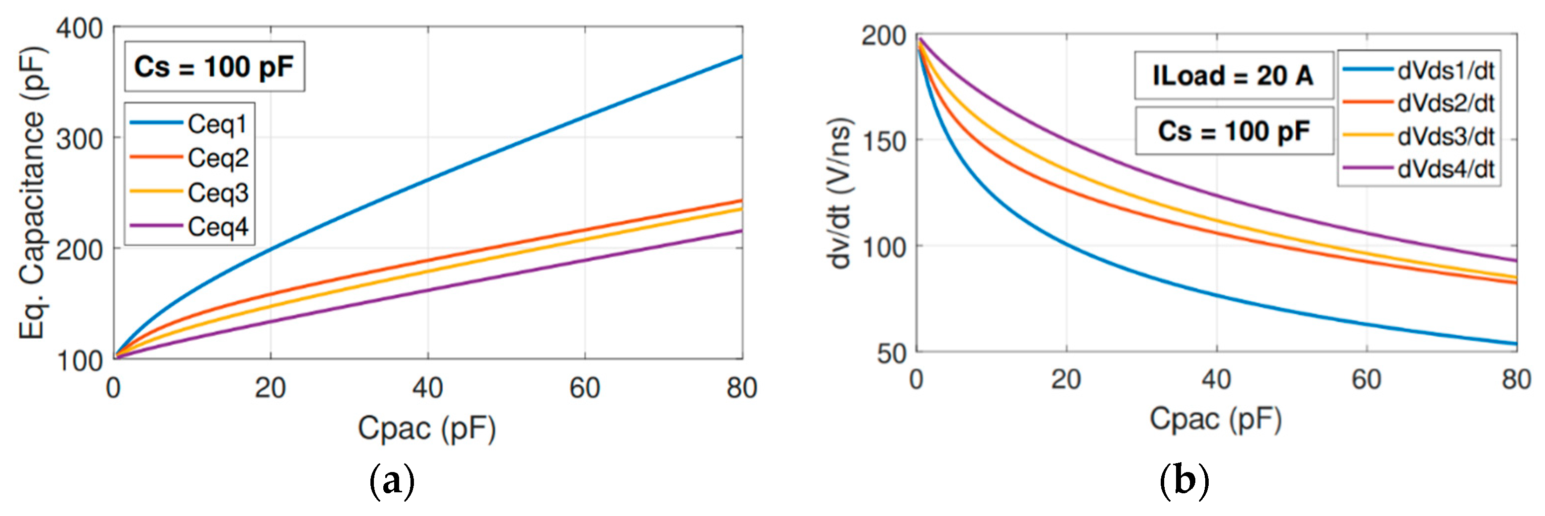
In
Figure 4a, the behavior of each equivalent parasitic capacitance as a function of
Cpac for
Cs = 100 pF is shown. This value is based on the datasheet of the device used in this work (C2M0160120 (1200 V, 19 A). As can be seen, the device at the top of the stack (S4) has the smallest equivalent capacitance (
Ceq4), whatever the
Cpac value is. On the other hand, the first device in the stack (S1) has the greatest equivalent capacitance (
Ceq1). Note that, the higher the device is positioned on the stack, the lower its drain-to-source equivalent capacitance is. The switching speed behavior of each device is also a function of its position in the stack as shown in
Figure 4b. In other words, the device at the top of the stack (S4) has the fastest switching speed, while S1 (the first one in the stack) has the slowest
dv/dt. This phenomenon has been observed in experimental results presented in the literature [
3,
7,
9,
11].
As can be seen in
Figure 4b, the devices have different switching speeds (
dv/dt) and, therefore, their voltages are dynamically unbalanced.
Electrical Transient Simulations: Traditional Planar Packaging
To validate the theoretical analyses done in the previous section, electrical simulations are made in LTSpice
TM software with four Cree
TM SiC-MOSFET Spice models C2M0160120 (1200V 19 A), which are switched under a total blocking voltage of 1 kV and a load current of 20 A. The simulations are done in the hypothetical case where the gate drivers are perfect, there is no time delay between the gate signals, and the power devices are identical. In other words, only the packaging/layout (capacitive elements) is taken into account. In
Figure 5, the simulation results for the traditional packaging/layout are shown.
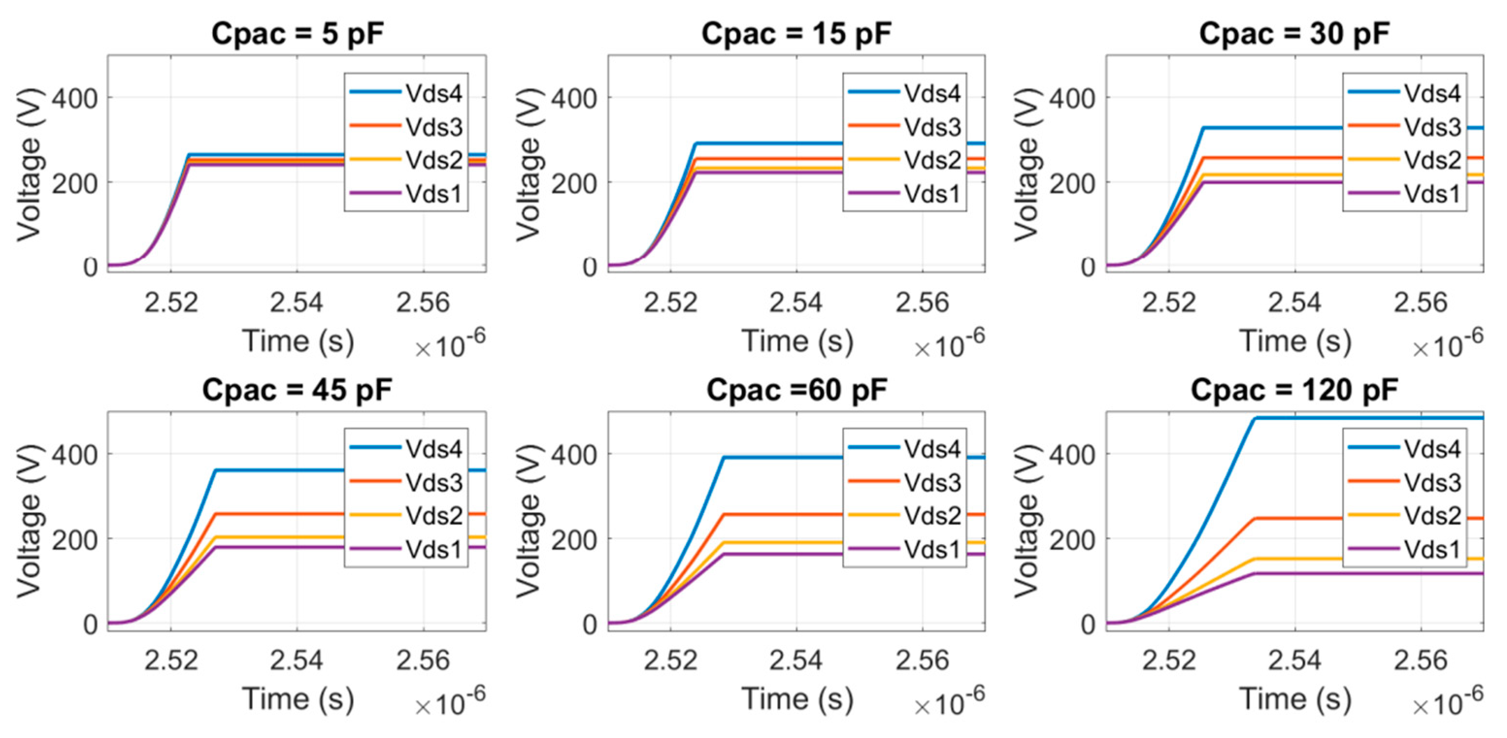
As expected, the voltage sharing in traditional packaging/layouts is drastically sensitive to the parasitic capacitances
Cpac. In
Figure 5 for
Cpac = 5 pF, an acceptable voltage unbalancing is presented. However,
Cpac = 5 pF is not a practical value; in traditional PCBs,
Cpac can reaches a few dozen pF, while in power modules,
Cpac can reach a few hundred pF [
18]. In this case, as shown in
Figure 5, from
Cpac = 30 pF to 120 pF, traditional packaging/layout exacerbates voltage balancing problems.
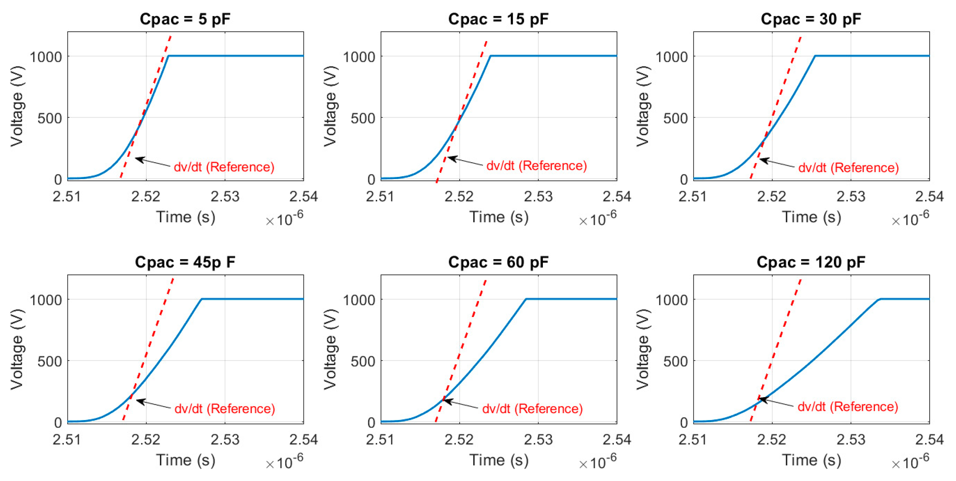
Another characteristic of classical package/layout is its impact on the switching speed of the devices. In
Figure 6, the simulation results of the
dv/dt of the switching cell as a function of the parasitic capacitance
Cpac are shown. A
dv/dt reference, which represents the
dv/dt for
Cpac = 5 pF, is placed in
Figure 6 to analyze the influence of
Cpac. As can be seen, the
dv/dt on the middle point is drastically reduced when
Cpac increases from 5 pF to 120 pF. As will be explained in the next section, modifying the parasitic capacitance configuration of the package/layout not only reduces the voltage unbalancing, but also can improve the switching speed of the devices.
3. Impact of Multi-Step Packaging Parasitic Capacitances on Voltage Balancing
As explained, the classical packaging/layout increases voltage balancing problems, since it generates unequal drain-to-source equivalent parasitic capacitances among the series-connected devices, which carry parasitic currents that get greater and greater with the device number in the stack (starting from the bottom). Therefore, to improve voltage balancing, the equivalent parasitic capacitances shown in
Figure 3c have to be identical, allowing the series-connected devices to have the same dynamic switching behaviors (
dv/dt).
To ensure equal drain-to-source equivalent capacitance distribution among the series-connected devices, a multi-step packaging (MSP) concept, shown in
Figure 7, is analyzed in this paper. The front and backside die-attachments are implemented in a similar way that is done in the traditional 2D planar package. As can be seen, in the MSP concept, the parasitic capacitances
Cpac are generated by the copper traces (connected to the drain contacts) of the series-connected devices.
The electrical scheme of the MSP is shown in
Figure 8a, where it is supposed that all SiC-MOSFETs are identical, and they are turning off. Note that, in the MSP configuration, the parasitic capacitances
Cpac are formed by two subsequent drain-attached copper tracers, i.e.,
Cpaci is the capacitance connected with drain–source terminals of the device S
i (for
i = 2,3,4). As shown in
Figure 8b, the high-frequency equivalent circuit can be simplified by short-circuiting the DC-bus terminals and
CY capacitors. Redrawing
Figure 8b, a further simplified high-frequency equivalent scheme can be achieved, as shown in
Figure 8c. The equivalent drain-to-source parasitic capacitances of each device are expressed by the Equations (8) and (9).
Analyzing
Figure 8c, the currents that circulate through the equivalent parasitic capacitances
Ceqi, can be expressed by the Equations (10) and (11).
where
Vdsi is the drain-to-source voltage across the device
Si, and
Vds5 is the middle point voltage.
To prove that the MSP can balance the voltages, it can be supposed that the voltages across the series-connected devices are perfectly balanced and find the
Cpaci values that ensure this supposition. Based on this assumption, it can be considered that the channel currents of series-connected devices are identical. Therefore, according to the mentioned considerations and the current distribution shown in
Figure 8c, the following equations can be written:
According to Equation (13), the series-connected SiC-MOSFETs can have the same switching speed behavior if the parasitic capacitances
Cpaci are identical. Therefore, to ensure an equal equivalent capacitance (drain-to-source) distribution among the series-connected devices, it is important to ensure that the Equation (14) is satisfied, i.e., once the isolated substrates are made of the same material, the ratio
A/
d has to be the same for all capacitances, where
A is the area of the copper trace where the SiC device is attached, and
d is the distance between two subsequent copper plates.
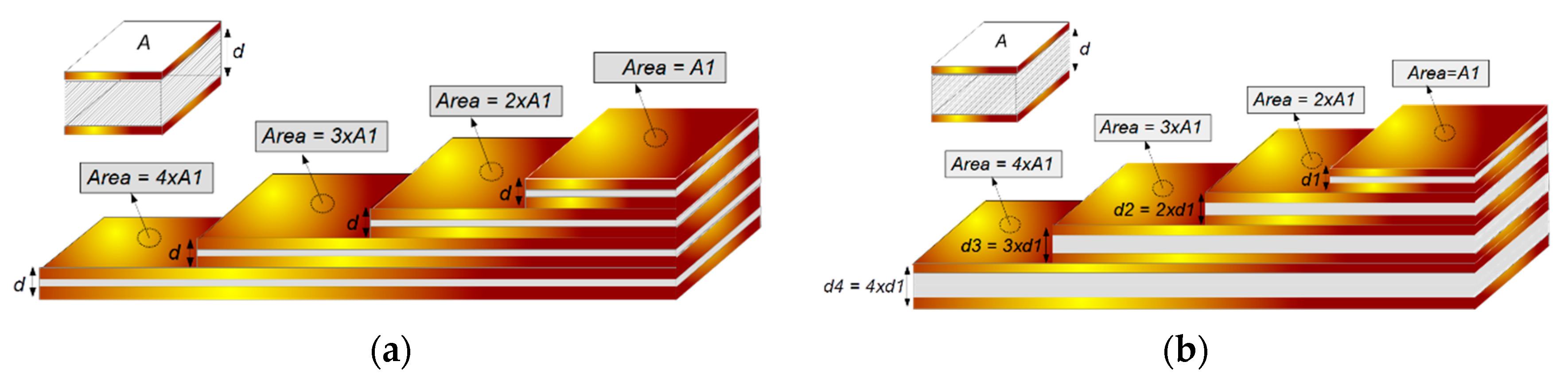
Figure 9 shows two 3D representations of the MSP that satisfy Equation (14).
Figure 9a shows a simple MSP/layout where the copper area (
A) of each floating potential is different from the others, assuming that the dielectric material thickness (
d) between them are the same. This simple solution induces different parasitic capacitances, since they have different ratios (
A/
d). Therefore, according to Equations (13) and (14), the voltage balancing cannot be ensured. In the second MSP geometry shown in
Figure 9b, the thicknesses of the dielectric material layer are adapted to keep the ratio
A/
d the same for all drain-to-source parasitic capacitances
Cpac, respecting the Equations (13) and (14). Another solution is to keep the same distance
d between all overlapping copper plates and the same area
A to ensure the same ratio
A/
d for all drain-to-source parasitic capacitances.
Therefore, considering that the parasitic capacitances
Cpac have the same value for all the series-connected devices, the Equation (13) becomes:
In this case, the negative impacts of the packaging/layout on voltage balancing are nullified, and the stacked devices can have the same switching speed behavior.
3.1. Electrical Transient Simulations of the Multi-Step Packaging
To validate the theoretical multi-step approach, electrical simulations are made in LTSpice
TM software with four Cree
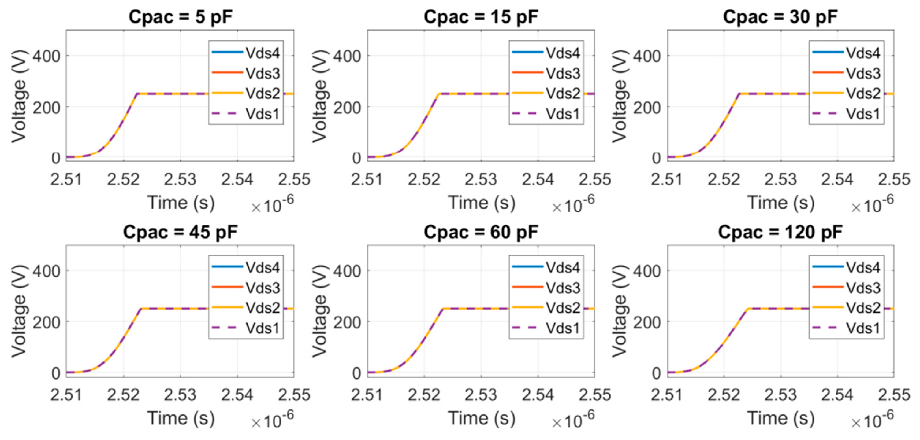
TM SiC-MOSFET Spice models C2M0160120 (1200 V 19 A), which are switched under a total blocking voltage of 1 kV and a load current of 20 A. The simulations are done in the hypothetical case where the gate drivers are perfect, no time delay between the gate signals is presented, and the power devices are identical. In other words, only the packaging/layout (capacitive elements) is taken into account. The simulation results are shown in
Figure 10.
As can be seen, the MSP is not sensitive to
Cpac in terms of voltage sharing among the series-connected devices, as shown in
Figure 10. Even for exacerbated values of
Cpac, the bus voltage is perfectly shared between the devices. The switching speed of the switching cell is also improved in the proposed MSP concept when compared to the traditional one.
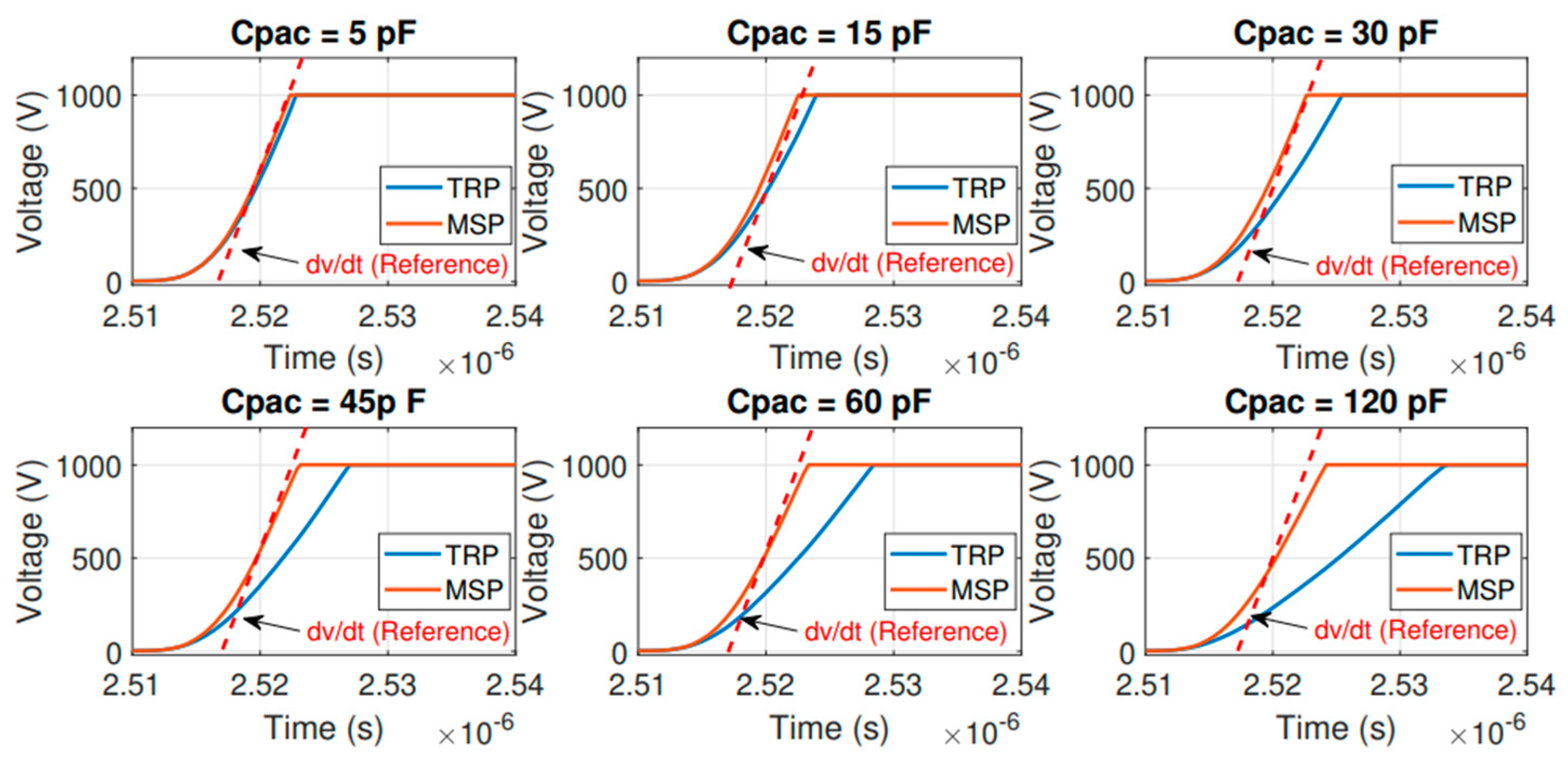
Figure 11 shows the
dv/dt as a function of
Cpac for the traditional (TRP) and MSPs/layouts. In the TRP, the parasitic capacitances
Cpac drastically impact the
dv/dt of the switching cell. On the other hand, the MSP concept is less sensitive to
Cpac. This is due the fact that in the TRP, the currents that circulate through the parasitic capacitances
Cpac are deflected from the switching cell to the ground or heatsink. In other words, a part of the currents that would be used to charge/discharge the device capacitances is deflected to the ground, slowing down the device switching speeds. On the other hand, in the MSP geometry, the currents that circulate through the parasitic capacitances
Cpac are returned locally to the switching cell.
3.2. Delay Time and Device Parameter Tolerance Sensitive Analysis
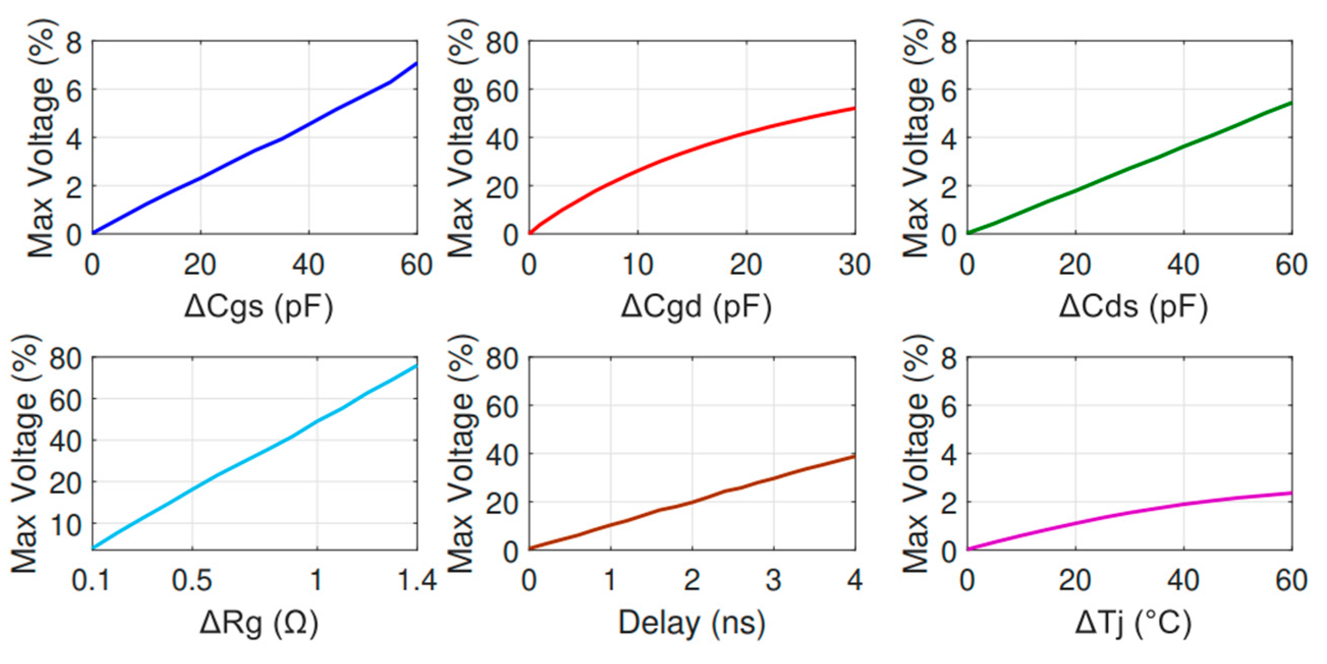
Up to now, it has been considered that there is no delay between the gate signals and no device parameter mismatch between the series-connected devices. Characterization and careful selections of SiC-MOSFETs can reduced the mismatch between SiC-MOSFET intrinsic capacitances. Optimized gate driver circuitry can mitigate the delay between gate signals. However, if these optimizations are not taken into account, it can drastically impact the MSP performance on voltage balancing. Therefore, a sensitive analysis is done in this section to estimate the impacts of the delay between gate signals and device parameter mismatch on the proposed MSP. Only two series-connected SiC-MOSFETs are analyzed so as to simplify the preliminary analysis.
To analyze the robustness of the MSP in terms of voltage balancing, the following parameters are used to perform the sensitive analysis:
∆Cgs, ∆Cgd, and ∆Cds, which represent the differences between the intrinsic capacitances of the series-connected devices. The values used in the analysis are based on a study performed in [
17,
19].
∆Rg, which represents the difference between the internal gate resistances of the devices. The values used in the analysis are based on a study performed in [
19].
Delay, which represents the delay between the gate signals.
∆Tj, which represents the junction temperature difference between the devices. As will be explained in this paper, in the MSP, each device has a different thermal resistance. Therefore, it can also impact the voltage balancing across the devices.
Two C2M
TM SiC-MOSFETs C2M0160120 (1200 V 19 A) are used in the analysis, where the top device parameters are fixed, and the parameter variations are imposed to the bottom device. The gate resistances are initially set to 10 Ω. The MSP parasitic capacitances are set to 30 pF. The series-connected devices are switched under a total blocking voltage of 1 kV and a load current of 20 A. The analysis is done in relation to the voltage across the top device, i.e., how much the top device voltage increases from the ideal voltage (half the bus voltage) to the final value caused by the parameter variation. The results, expressed in percentage (%), are shown in
Figure 12. As can be seen, the mismatch between the intrinsic capacitances
Cgs slightly impacts the voltage balancing. Every 20 pF of difference, the top device voltage increases only by 2%. The mismatch between the intrinsic capacitances
Cds has a similar impact on voltage balancing. On the other hand, the mismatch between the intrinsic capacitances
Cgd drastically increases the voltage unbalancing. For ∆C
gd = 20 pF the top device voltage increases by 40%. In other words, if the bus voltage is equal to 1 kV, the top devices experience a drain-to-source voltage of 700 V. This is understandable, since during the switching transition (Miller plateau,
vds rising/falling), the switching speed behavior is very dependent of
Cgd, i.e., the switching speed represents the necessary time to charge/discharge
Cgd.
The mismatch between internal gate resistances also drastically impacts voltage unbalancing. A ∆Rg = 0.5 Ω is enough to increase the top voltage device by 20%. Unlike the device-intrinsic capacitances, the device’s internal gate resistance is constant and does not dependent on Vds voltage. After a careful device characterization, the mismatch between internal gate resistances can be compensated by external ones.
The delays between gate signals have also an important influence on the voltage balancing. As can be seen in
Figure 12, four nanoseconds are enough to increase the top device voltage unbalance of 40%. Therefore, optimized gate signal circuitry is required to improve the voltage balancing across the series-connected SiC-MOSFETs.
The junction temperature difference among the devices is another important parameter for the MSP, since each device in the stack has a different thermal resistance. The main device parameters that are influenced by the junction temperature
Tj are the drain-to-source current
IDS, the drain-to-source on-state resistance
RDSon, and the threshold voltage
VTH. However, according to the SiC-MOSFET C2M0160120 datasheet, a large variation on the junction temperature to generate proportional variations on the device parameters is necessary. For example, according to C2M0160120 datasheet, the
VTH variation as a function of
Tj is only 0.005 V/°C. This robust stability is validated by simulation results, as can be seen in
Figure 12, where even for exacerbated values of ∆T
j the top device voltage does not increase considerably.
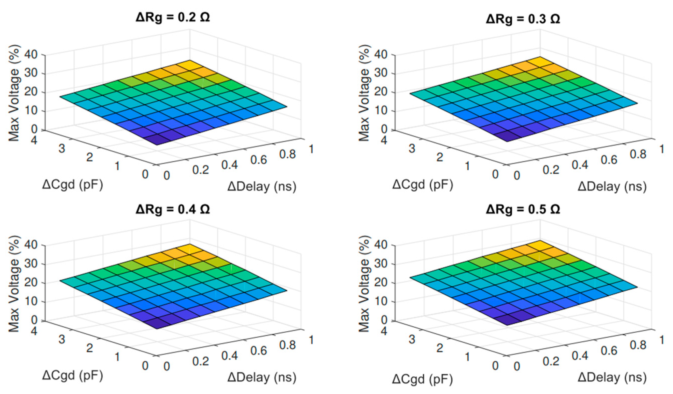
Based on the sensitive analysis shown in
Figure 12, ∆C
gd, ∆R
g, and ∆delay are the three most important parameters that can considerably increase voltage balancing problems. In order to analyze the impact of C
gd, ∆R
g, and ∆delay on voltage balancing,
Figure 13 shows the sensitive analysis of these three parameters, where their variations are analyzed together. The main idea is to vary, at the same time, ∆C
gd, ∆R
g, and ∆delay in order to reach the worst case and then to know the acceptable device mismatch limits. The analysis is done for four values of ∆R
g: 0.2, 0.3, 0.4, and 0.5 Ω. The ∆C
gd is changed from 0 to 4 pF, and ∆delay from 0 to 1 ns. The analysis is done in the same manner presented in
Figure 12, i.e., it is investigated how much the top device voltage increases from the ideal voltage (half the bus voltage) to the final value caused by the parameter variation.
As can be seen in
Figure 13, the MSP can provide good voltage balancing if these parameters are limited according to acceptable levels of voltage unbalancing. For example, supposing that it is acceptable that the top device in the stack takes 20% more than the ideal voltage (half the bus voltage), and ∆R
g is limited to 0.2 Ω. For ∆C
gd values ≤ 4 pF and ∆delay values ≤ 0.4 ns, the top device voltage will not increase more than 20%, ensuring a good and acceptable voltage balancing across the series-connected SiC-MOSFETs.
It is important to note that the faster the SiC-MOSFETs switch, the more the parameters impact the voltage balancing. The sensitive analysis presented here is done under a hard switching operation, where discrete device models (C2M0160120) are used. For power devices that switch more slowly, such as some SiC/Si power modules or IGBTs, these parameters have less influence, and the MSP is less sensitive to the parameter mismatches. On the other hand, for devices that switch very quickly, such as GaN transistors, the analyzed parameters have more influence, and the MSP is more sensitive to the parameter mismatches.
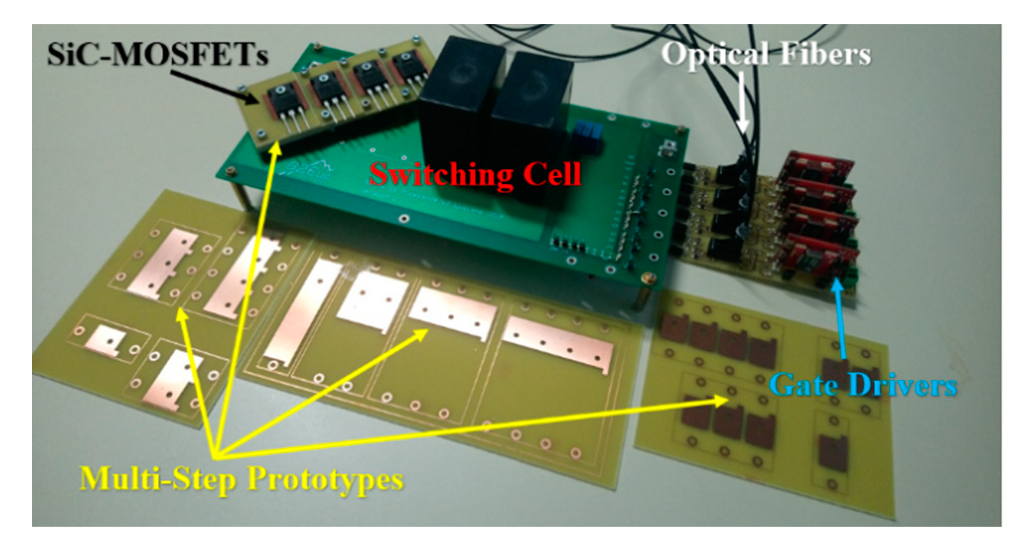
4. Experimental Results
To investigate the theoretical approach proposed in this paper, two prototypes have been developed. These prototypes, i.e., the MPS package and planar one, are built thanks to stacked FR4 layers so as to verify the electrical behaviors without thermal considerations. Therefore, these prototypes are used in a pulsed mode to avoid a significant temperature increase in the SiC-MOSFETs. The developed prototypes meet the following requirements:
Each copper plate where each SiC device is attached has the same area—A = 10 cm2.
The FR4 dielectric thicknesses between two copper plates, which generate each Cpac, are all the same—d = 1.5 mm.
The isolated substrates are made of the same FR4 material, and they have the same absolute permittivity—ɛ = 45 pF/m.
The measured parasitic capacitances between two copper plates are almost the same for the MSP prototype—Cpac = 30 pF (discrepancy < 5% between these capacitances).
The traditional packaging also introduces a parasitic capacitance Cpac of 30 pF.
As shown in
Figure 14, a switching cell with four series-connected SiC-MOSFETs C2M0160120 (1200 V, 19 A) and one diode STPSC40H12CWL (1200 V, 20 A) has been used to investigate the influence of the traditional packaging and the proposed package concept on the voltage balancing and on
dv/dt. A bus voltage of 1 kV and a load current of 20 A have been used in the experiments. No external drain-to-source resistor are added to provide static voltage balancing. In order to mitigate the impact of the gate driver to ground parasitic capacitances in the set-up experiments [
3], the gate drivers shown in
Figure 14 are powered by batteries.
The delay time and the effects of voltage probes are compensated by a specific calibration process, where the power devices are left with no connection to the FR4 package. In this situation, it is supposed that the parasitic capacitance
Cpac has an ultra-low value, although it is probably still different to zero. Adaptative open-loop external delay and gate resistance circuits are implemented to achieve a perfect voltage sharing between the devices. In this case (CASE 1), all effects generated by the gate drivers, voltage probes, the different characteristics between the devices, etc., are compensated. The switching speed calibration result is illustrated in
Figure 15. As can be seen in
Figure 15a, balanced voltages of around 250 V are achieved with a very small discrepancy (<15 V) between them. In
Figure 15b, the zoomed dynamic phase is shown. These waveforms are the reference point to analyze the classical planar package and the MSP one, since these results are achieved without any FR4 package. The results shown in
Figure 15 are in accordance with the theoretical analysis presented in
Section 2. It can be verified making
Cpac tend to zero in Equations (3)–(6). In this case, the series-connected SiC-MOSFETs have the same drain-source equivalent parasitic capacitance (
Cs) and, therefore, the same switching speed behavior, leading to balanced voltages across the devices.
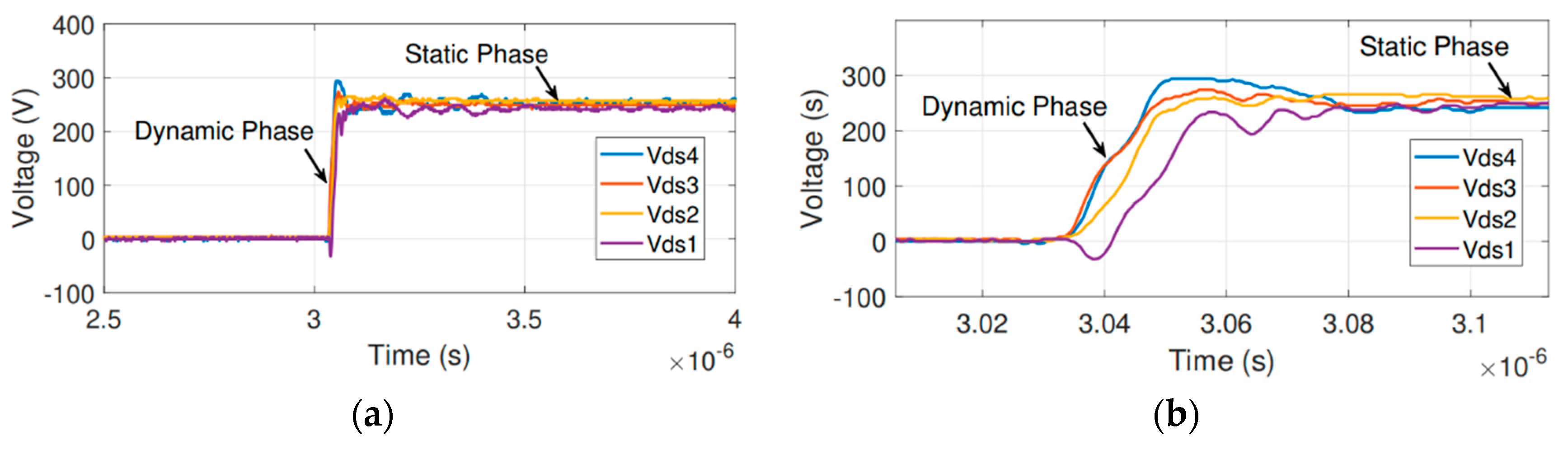
According to the theoretical analyses presented in this paper, the parasitic capacitances introduced by the classical planar packaging can unbalance the voltages across the series-connected SiC-MOSFETs, even if there are no delays between gate signals and no mismatch between the characteristics of the series-connected devices. This theoretical analysis is experimentally validated, as shown in
Figure 16. According to the Equations (3)–(6) and
Figure 4, when the classical planar packaging is implemented for the device’s assembly and interconnects (CASE 2), unequal
dv/dt that are a function of the position of devices in the stack, are applied to the parasitic capacitances introduced among the series-connected SiC-MOSFETs. It produces parasitic currents that are also a function of the position of devices in the stack. As expressed in the theoretical analysis, the experiments validate that behavioral representation leads to voltage balancing problems, as shown in
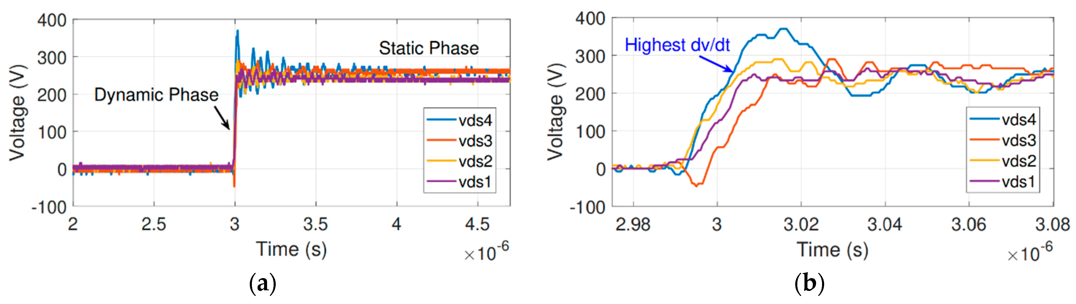
Figure 16. As can be seen in
Figure 16a, the parasitic capacitances introduced by the traditional planar package produce an important voltage unbalancing. A considerable voltage difference of around 110 V is observed between the drain-to-source voltages (
Vds4 – Vds1) across the series-connected devices. Note that, the parasitic capacitance
Cpac in the traditional package prototype is only 30 pF. Classical power modules can introduce a few hundred pF, which will exacerbate voltage balancing problems.
Figure 16b shows the zoomed view at turn-off. As mentioned in this paper, and according to the Equations (3)–(6) and
Figure 4, the highest device on the stack takes the largest portion of the bus voltage. This phenomenon repeats itself in the present experiments where
Vds4 is approximately equal to 360 V, which represents approximately 44 % more than the ideal voltage (250 V).
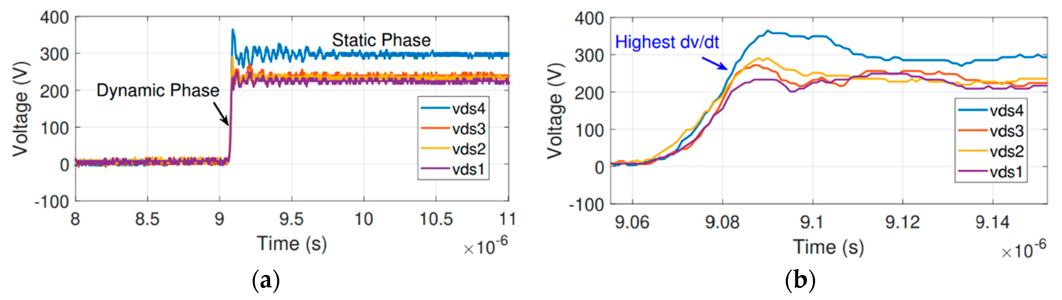
Figure 17 shows the experimental results when the MSP is attached to the switching cell (CASE 3). As expected, the voltage unbalancing has been drastically reduced. A small voltage difference of around 31 V is observed between the drain-to-source voltages (
Vds4 –
Vds1) across the devices. As well as in CASE 2, the highest device on the stack (S4) still takes the largest portion of the DC bus voltage. However, in CASE 3, the V
ds4 is approximately 265 V. It represents no more than 6% in relation to the ideal voltage (250 V). These results are in accordance with the theoretical analysis presented in
Section 3, i.e., the MSP introduces equal drain-source equivalent parasitic capacitances across the series-connected SiC-MOSFETs. In addition,
dv/dt are not anymore dependent of the device number in the stack, which implies the same switching speed behavior among them as described by Equation (15). Therefore, the voltage balancing problems introduced by the package capacitances are drastically reduced, as shown in
Figure 17.
Note that, in the three cases, the peak voltage during the turn-off switching is caused by the stray inductance of the switching cell. In this case, as no static resistors are used in the experiments, the discrepancy between the Vds voltages is measured after the ringing voltage.
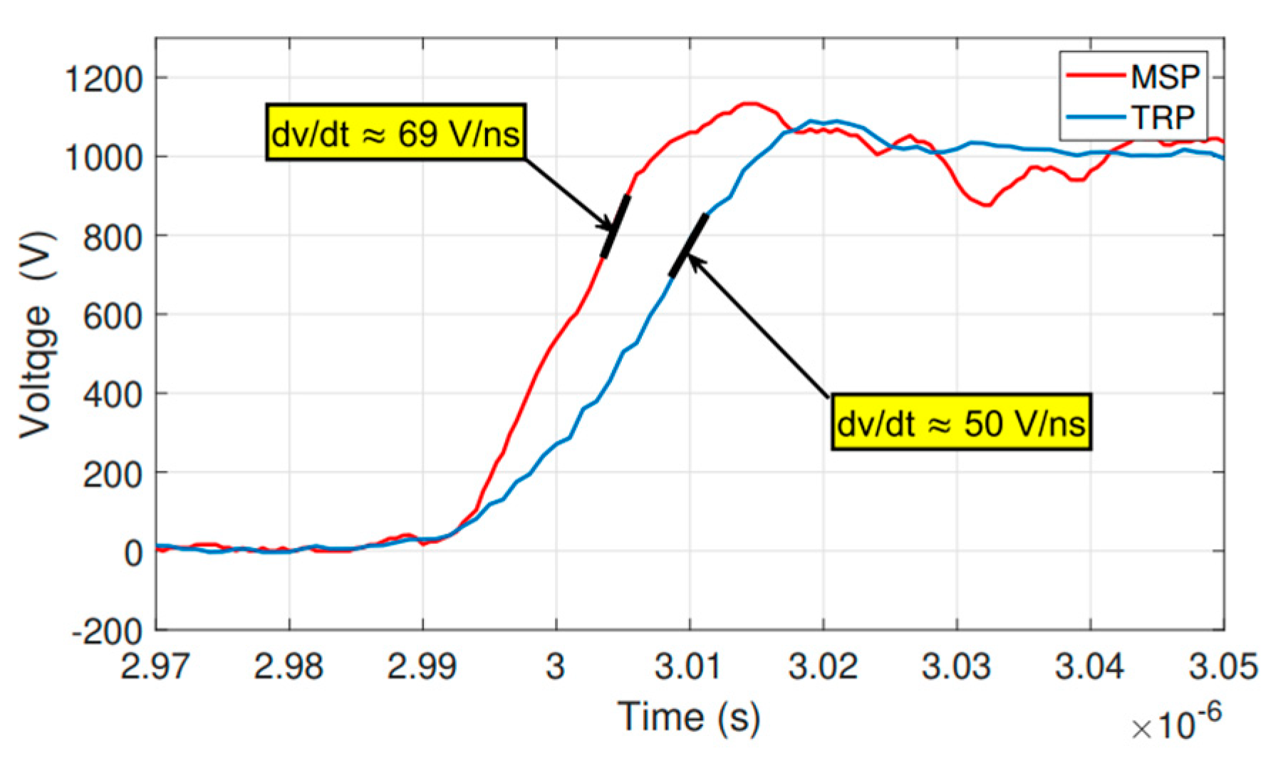
In
Section 3, the simulation results depicted in
Figure 11 show that the MSP can increase the middle point switching speed when compared to the TRP one. These results are also experimentally validated. In
Figure 18, the experimental results for both packages in terms of
dv/dt are shown. As can be seen, the switching speed on the middle point of the switching cell has been boosted from 50.0 V/ns to 69 V/ns. It represents a gain of 38% on the
dv/dt of the switching cell, which may produce a significant gain in terms of switching losses. These results can be explained by the theoretical analyses represented by
Figure 3b and
Figure 8b. In the TRP represented by
Figure 3b, the currents that circulate through the parasitic capacitances
Cpac are deflected from the switching cell to the ground or heatsink. Therefore, a part of the currents that would be used to charge/discharge the device capacitances is deflected to the ground, slowing down the device switching speeds. On the other hand, in the MSP geometry represented by
Figure 8b, the currents that circulate through the parasitic capacitances
Cpac are all equal and they return locally to the switching cell, which maintains the switching speed of all the devices in the stack when compared to the classical planar package.
As can be seen, when the proposed MSP is applied for series-connected SiC-MOSFETs, it can mitigate voltage-balancing problems and also improve the switching speed when compared to the classical planar packaging. However, to explore the MSP at its full potential, thermal aspects have to be taken into account.
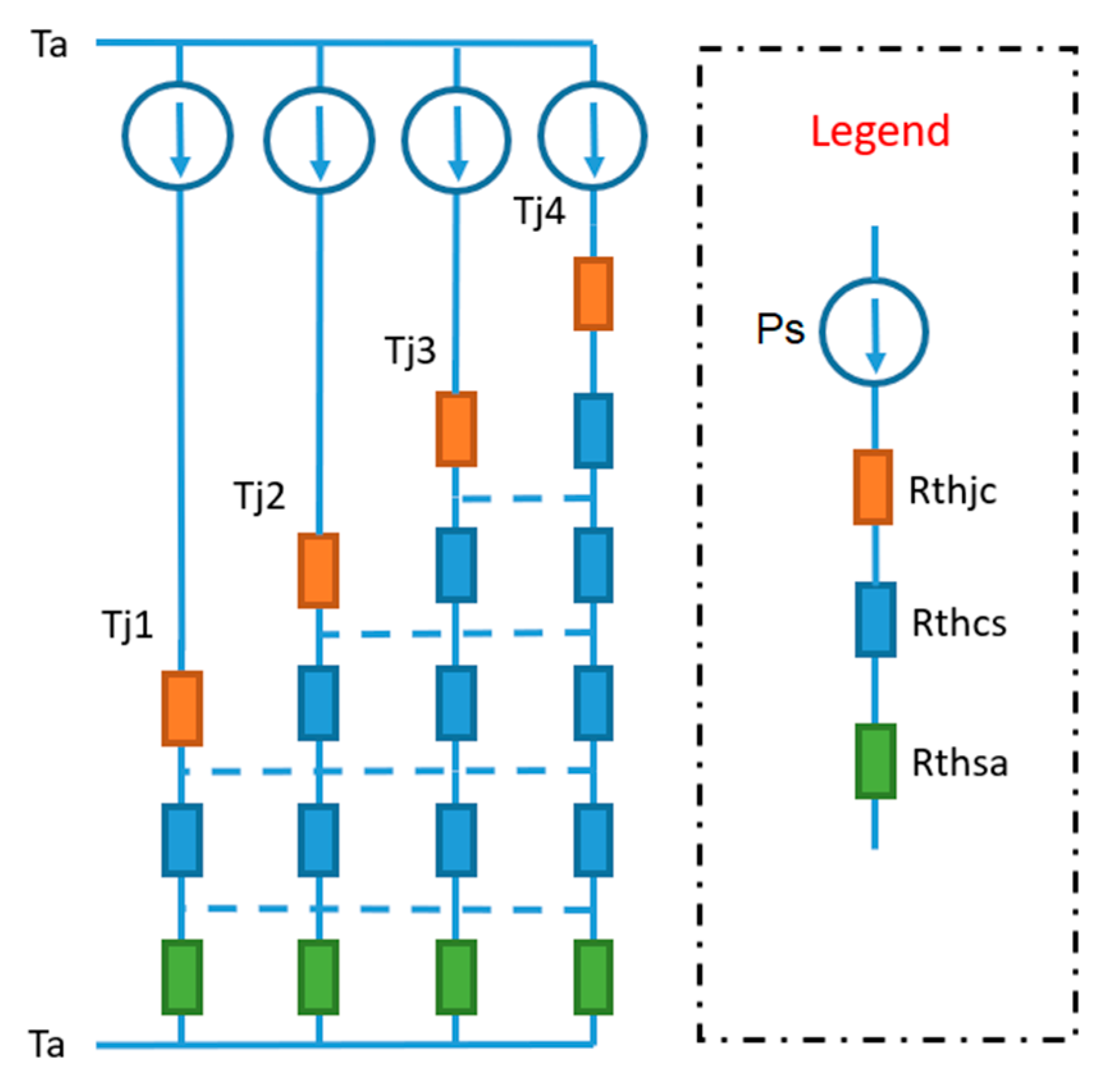
5. Thermal Management Considerations
The MSP introduces nonhomogeneous propagation paths for the heat flux from each device to ambient. The addition of several dielectric layers, along with the number of steps, brings an increase in the junction-to-ambient thermal resistance, which produces an increase in junction temperature T
j for the devices “above” with respect to the “bottom” device, the one located closer to the heat sink. This temperature increase is dependent on the heat flux and the characteristics of the additional dielectric layers. The lower the thermal resistance of the dielectric layer is, the lower the impact on the junction temperature will be. In addition, the lower the thermal resistance of the additional dielectric layer (s) is with respect to the remaining thermal resistance on the pathway of the heat, the lower the impact of the additional layers will be. A simple first order 1D thermal model can be developed to investigate this issue, as shown in
Figure 19, where:
TjN is the junction temperature of the device N, “1” being the bottom device and “2, 3 and 4” being the other “above” devices.
Ta is the ambient temperature.
Ps is the dissipation source in each device, representing the power losses, considered in this example as all equal.
Rthjc is the junction-to-case thermal resistance (mainly the die itself and the die attach).
Rthcs is the case-to-sink thermal resistance (mainly the dielectric layers).
Rthsa is the heatsink thermal resistance (mainly the heat sink, including thermal grease).
Based on the equivalent circuit presented in
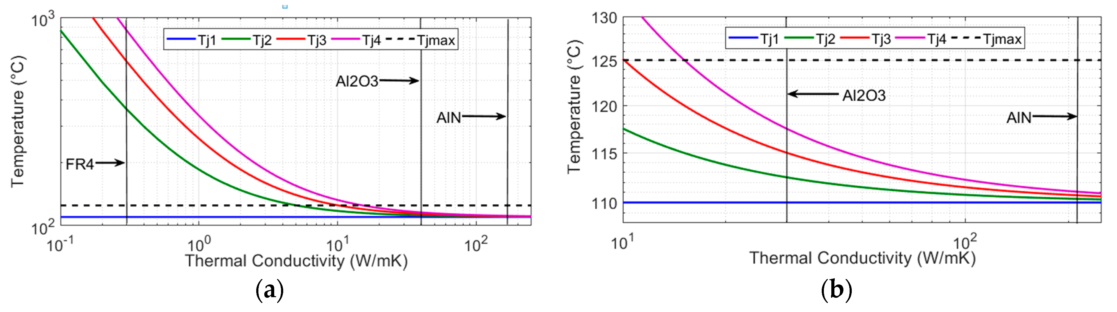
Figure 19, the junction temperatures of the devices 2, 3, and 4 increase with respect to device 1. In
Figure 20, a graph plots the impact of the thermal conductivity of the dielectric layer and its impact over junction temperature rise in MSP module. Some values used to calculate the junction temperature increase among the series-connected devices are based on the datasheet of the device used in the experiments, which leads to R
thjc of 0.1/°C and a cross-section through the dielectric layer of 17 × 14 mm
2. The thickness of the dielectric material is considered constant and equal to 300 µm. It is also supposed that T
a = 25 °C, and the maximum acceptable junction temperature T
jmax is equal to 125 °C. Three dielectric materials are analyzed in
Figure 20. A heat flux of 60 W is considered in the present analysis.
As can be seen in
Figure 20a, the temperature increase among the devices is drastically dependent on the thermal conductivity of the dielectric material (K
T). Considering a heat flux P
s of 60 W and a dielectric composed by the FR4 material, the junction temperature distribution over the four power devices is unacceptable. A utopian R
thsa ≈ −15.5/°C would be needed to keep the temperature among the devices below 110 °C. This is due to the very low thermal conductivity of FR4, i.e., K
T ≈ 0.3 W/mK. However, if other dielectric materials with better thermal resistance are used, such as AlN and Al
2O
3, the junction temperature distribution over the four power devices can be drastically reduced. As shown in
Figure 20b, which is a zoom of
Figure 20a, considering P
s equal to 60 W, a R
thsa equal to 1.27/°C per device for planar design, and Tj = 110 °C for Al
2O
3 dielectric layers (K
T ≈ 25 W/mK), the impact on T
J4 is limited, with the temperature rise up to 10 °C. In the same way, for 300 µm AlN dielectric layers (K
T ≈ 220 W/mK) the impact on Tj4 is even more limited to 1 °C. Taking into account the impact of a T
j rise on device power losses, the resulting total temperature increase is up to 15 °C for Al
2O
3 dielectric layers and 2.7 °C for AlN dielectric materials.
It is important to note that these results are highly dependent on heat flux and heat sink design. However, this brief analysis shows that if the additional dielectric layers have small thermal resistances with respect to the other thermal resistance on the path of the heat flux, then the MSP has a limited impact on the distribution of the junction temperatures
Tj of the devices implemented on each step of the power module. Neglecting the impact of junction temperature over component losses, if each additional dielectric layer introduces a thermal resistance X% of the total thermal resistance from
Tj to
Ta, then the impact on
Tj rise per step is limited to X%. This would have a very limited impact on voltage sharing, as illustrated on
Figure 12. If the junction temperature rise exceeds 5 to 10%, the impact on component losses could be taken into account to verify that the final junction temperature rise for each component implemented in the MSP remains below the maximum junction temperature.

 ,
, 


