Article

3D Printed Electronic Circuits from Fusible Alloys

Micro- and Nanotechnology Division, Institute of Metrology and Biomedical Engineering, Faculty of Mechatronics, Warsaw University of Technology, 8 sw. A Boboli St., 02-525 Warsaw, Poland
*
Author to whom correspondence should be addressed.
Electronics 2022, 11(22), 3829; https://doi.org/10.3390/electronics11223829
Submission received: 2 November 2022 / Revised: 10 November 2022 / Accepted: 18 November 2022 / Published: 21 November 2022
(This article belongs to the Special Issue New Trends in 3D Printing for Novel Materials)

Abstract

:
This work aims to evaluate the possibility of fabricating conductive paths for printed circuit boards from low-temperature melting metal alloys on low-temperature 3D printed substrates and mounting through-hole electronic components using the fused deposition modeling for metals (FDMm) for structural electronics applications. The conductive materials are flux-cored solder wires Sn60Pb40 and Sn99Ag0.3Cu0.7. The deposition was achieved with a specially adapted nozzle. A comparison of solder wires with and without flux cores is discussed to determine whether the solder alloys exhibit adequate wettability and adhesion to the polymer substrate. The symmetrical astable multivibrator circuit based on bipolar junction transistors (BJT) was fabricated to demonstrate the possibility of simultaneous production of conductive tracks and through-hole mountings with this additive technique. Additional perspectives for applying this technique to 3D-printed structural electronic circuits are also discussed.

1. Introduction

Structural electronics is a term describing electrical and electronic components and circuits that act as construction elements, casings, or other types of protective dumb structures, such as vehicle bodies, and are embedded inside the volume of an element or conformally placed on the surface. Due to the possibility of enhancing product functionality, lowering production costs, or providing the opportunity for the fabrication of consumer-tailored devices, structural electronics is an interesting new branch of technology for ordinary production methods used in aerospace and military applications, home appliances, consumer electronics, the automotive industry, and civil engineering. A catchy example of structural electronics is the new Saint Anthony Falls Bridge in Minnesota, US, called America’s smartest bridge [1]. The previous one collapsed in 2007, so the new one is stuffed with sensors monitoring its condition. The TactoTek company introduced a complete production chain from design to fabrication of fully functional injection molded and structural electronics using DuPont conductive materials [2]. Ford introduced an overhead control cluster fabricated with in-mold electronics in the automotive industry, saving up to 40 % in weight/space/cost and increasing reliability [3].
One of the disruptive manufacturing techniques that significantly impact many fields of technology is additive manufacturing, also called rapid prototyping or 3D printing. It allows fabricating objects directly from digital computer-aided design (CAD) files without molding or subtractive milling. It enables the creation of complex geometric parts, permits fast and flexible design changes, the rapid development of mass customization, and a low-risk entrance of innovations to the market. 3D printing technology involves a layer-by-layer construction of the element in a number of ways depending on the printer being used [4,5]. Powder spread on a tray can be solidified in the desired pattern with a liquid binder [6], sintered with a laser [7], or electron beams [8]. Layers can be fabricated with 3D lithography processes from photosensitive resins [9] or deposited from filaments of fused polymers [10]. The world is also seeing rapid advances in 3D printing technology, with manufactured items created from plastic [11], ceramics [12], metal [13], or unusual ingredients, such as sugar, various types of food [14], and living tissues [15].
Additive manufacturing is nowadays widely used in many manufacturing sectors, from aerospace and the automotive industry to bioengineering and architecture [16,17,18,19,20]. Most 3D printers build elements from one type of material. They cannot build objects with electronic, optical, or any kind of functions that require integrating multiple materials. In parallel to 3D printing, we deal with printed electronics, another revolutionary additive technology involving the vast experience of the printing industry. Many electronic solutions have been produced with printed electronics techniques for years, including RFID tags [21,22,23], photovoltaic cells [24,25,26,27], sensors [28,29,30,31], electroluminescent displays [32,33,34,35], batteries [36,37], capacitors [38,39,40] and many others. As an additive technology, it allows more efficient utilization of materials. The primary limitation is the deposition of functional material only on flat substrates, though flexible circuits are also possible. Combining the results of additive manufacturing and printed electronics, the concepts for integrating 3D printing and conductive materials for producing functional, monolithic 3D structures with embedded electronics emerged. Structural electronics produced by 3D printing will function much, such as printed electronics, with the advantage of producing 3D objects with wires and circuitry embedded in a volume of elements. This allows designers to create smaller, lighter, more efficient, and customized products. To achieve this goal, low-cost, easy-to-use functional materials and 3D printing methodologies are required.
Functional materials are crucial to the rapid development of 3D printed structural electronics. The most investigated group of materials are conductive thermoplastic filaments, conductive inks, and pastes. At this time, companies working on supplying such technologies to the market have narrow and straightforward objectives—the lowest possible resistivity. In the literature, we find experiments towards conductive composites for fused deposition modeling with graphene [41,42], carbon black [43], carbon nanotubes [44] as a conductive filler, and in the form of composite inks and pastes with various carbon nanofillers [45,46,47] and graphene [45]. At this time, no major breakthrough was presented. The primary obstacle for materials branded as “conductive filaments” or “carbon conductive pastes” is high resistivity. Such materials exhibit resistivity in the range from 102 Ωm [42] down to 10−2 Ωm [44]. Therefore, as an alternative approach, a metallic powder as a filler is also used to achieve higher electrical conductivity in the final composite. The majority of examples of composite filaments containing metal powders reported so far in the literature focus on their mechanical properties. Such composites can be used as construction materials, but they are not materials that could be applied to structural electronics as electrically conductive composites. Recent studies of using FDM technology to print metal use metal-infused powder polymer filaments that can be fabricated using regular o-modified fused deposition modeling printers to form 3D structures. After 3D printing, the polymer content of the fabricated part is removed, and the green part is sintered, leaving a pure metal object. However, such a process still requires subsequent steps after printing to remove the polymer and get the final metal part [48].
One of the lowest resistivities reported for polymer composites filed with metal powders printed with the FDM technique was for composite filaments with copper powder as a conductive phase. Results show that the lowest resistivity (1.56 × 10⁻⁴ Ωm) was achieved for the ABS/Cu composite at 84.6 wt.% Cu concentration [49]. Such composites are brittle and difficult to print, presenting limitations for final electronic applications.
The Cornell University team, US, presented a different approach where FDM and Direct Write fabrication processes were utilized to form a fully functional loudspeaker [50]. One printer (FDM) made the plastic cone and base of the loudspeaker, and the second printer (Direct Write) laid down the coil with silver paste and created a magnet from strontium ferrite ink. One of the best examples of a 3D printed structural electronic system was demonstrated by a team from the University of California Berkeley, US, in collaboration with Taiwan’s National Chiao Tung University. Their impressive portfolio of 3D printed resistors, inductors, and capacitors was expanded by printing a wireless “smart cap” for a milk package that detected signs of spoilage using embedded sensors [42,51]. They printed polymer 3D structures with wax as a sacrificial material to define the passive components, melted the wax, and filled the resulting vacancies with the silver paste using a syringe, so the electrical paths were not entirely 3D printed. Additionally, an electronic circuit was fabricated for a university-based satellite, based on the same technique of direct write of silver paste, this time inside a 3D printed substrate with machined grooves for an electrical circuit [52]. These techniques also have limitations, while the resistivity of conductive paths from silver pastes is still a few orders of magnitude higher than for bulk metals (above 10−5 Ωm). Therefore a team from Harvard University and spin-off Voxel8 presented a complete system that uses FDM and Direct Write of low-viscosity, reactive silver inks based on AgC2H3O2, curable at 90°C, exhibiting an electrical resistivity in the range of 10−6 Ωm [53]. The primary limitation of this technique is the use of composite silver pastes, which are expensive and do not provide the expected low resistivity and metallic conductivity of the electrical paths.
An alternative approach for low-resistivity circuits could be the direct deposition of metals along with fused polymers. Metals have been used in additive manufacturing for decades in the form of powders (titanium, steel, etc.), sintered or melted together with high-power lasers or electrons in high-temperature processes. The currently popular AM technologies for making metal components mainly focus on the high-melting-point metals, where the laser, arc welding, or electron beam is selected as the heat source [8,54,55,56] and the metal powder or metal wire is supplied as the additive material [57,58,59]. Limitations of powder-based and wire-feed AM techniques lie in the relatively high cost of the instruments, high energy consumption, lower usage efficiencies of material, and structure defects from residual stresses and distortions.
However, on the other hand, low-temperature melting of metals and alloys is also employed in additive manufacturing. A molten metal droplets deposition technique, similar to ink-jet, was elaborated to fabricate 3D structures from Sn material [60], with very impressive results. Therefore, the idea to use low-temperature metals or alloys for FDM emerged. Such an approach involves adapting solder alloys, such as SnAgCu, for consumer-level FDM printers that typically extrude molten thermoplastics at 250 °C—the same temperature that melts solder alloys. This way, mechanical parts have been fabricated, both directly through 3D printing [61] and with the additional molding step [62]. In 2009 at the University of Bath, this approach was tested, providing a simple form of FDM-printed electronic circuits [63]. This simple 2D circuit was deposited on a flat ABS substrate, also created with FDM. A similar approach involved a detailed analysis of several commercial low-temperature melting alloys. Six commercially available alloys (Bi36Pb32Sn31Ag1, Bi58Sn42, Sn63Pb37, Sn50Pb50, Sn60Bi40, and Sn96.5Ag3.5) were tested for the creation of a fused deposition model on an existing Stratasys FDM 3000 system [64]. Deposition of 2D circuits was achieved through specific modifications to system toolpath commands. The same team also fabricated 3-dimensional metallic structures from eutectic Bi58Sn42 and non-eutectic Sn60Bi40 materials [65]. Both of these experiments were focused on the technical aspect of deposition with proprietary hardware and the demonstration of the possibility of fabricating circuit-like patterns, without additional analysis of the metal-substrate interaction or analysis of electrical properties and applications.
Concluding electrically conductive paths and elements in 3D printed electronics are usually prepared from polymer composites filled with carbon or metal additives for FDM (high resistivity) or silver pastes for Direct Write (expensive materials). Fusible alloys used with the FDM technique are used primarily to fabricate construction elements. Here, we propose a new approach to implement fusible alloys for the fabrication of conductive paths inside 3D printed polymer structures, required for high-performance structural electronics, outperforming the state-of-the-art silver pastes, metal and carbon-filled composites, matching the performance of printed circuits boards, with parameters suitable for electronic or electrical applications. The goal is to evaluate interactions between molten alloy and a 3D-printed polymer substrate during the deposition process. We already know that the extrusion of fusible alloys is possible with minimal technical effort, but the major challenge is to incorporate metals and alloys with FDM to help build electronic circuits with superior parameters suitable for the soldering of electronic components and to fabricate functional electronic circuits.

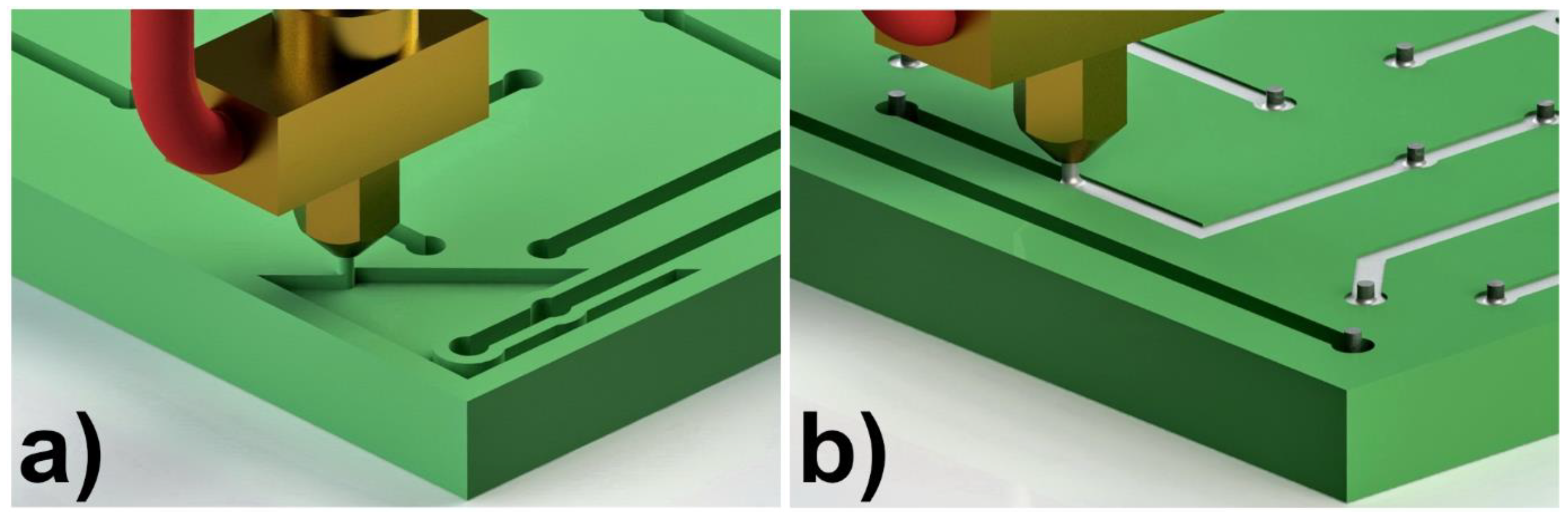
2. Materials and Methods

This work aims to evaluate the possibility of producing PCB’s conductive tracks and mounting through-hole electronic components using the fused deposition modeling of metals (FDMm) method on 3D printed substrates from ABS polymer. The ABS thermoplastic material (poly(acrylonitrile-co-butadiene-co-styrene)) was acquired from Plastaw, Poland. Polymer substrate was printed with a 3D Graften Pro printer (Graften, Poland). The conductive materials are solder alloys of Sn60Pb40 and Sn99Ag0.3Cu0.7. Used solder alloys exhibit electrical conductivity equal to 0.153 µΩm and 0.126 µΩm, along with thermal conductivity of 49 W/mK and 66 W/mK, respectively. Electrical measurements of the output waveforms for the multivibrator were performed with a Rigol DS1054Z oscilloscope (Rigol, Portland, OR, USA).
By the name FDMm, we define a variation of FDM in which the polymer filament is replaced with metal or alloy wire. The principle of operation of this FDM variant is the same as the original technology. The difference in changing the filament from a polymeric material to a metal equivalent relates to how it behaves during the printing process. This variation of additive manufacturing technology is far less common than traditional FDM printing. One of the main differences resulting from the change in material from polymer to metal is that, in the case of a polymer, it is only plasticized at the time of extrusion, while in FDMm technology, the metal must be completely melted. This results in a much lower viscosity of the applied material during FDMm printing. This can cause significant problems in keeping the width and height of the overlay path constant and maintaining the manufactured part’s geometry when overlaying successive layers. Another problem related to metal printing is the wettability of the printing nozzle. The nozzle must be composed of a material with low wettability for the metal, or metal alloy is used to allow it to flow freely. Otherwise, the nozzle will clog, and the printing process will not be possible.
The general concept of the FDMm technique and the fabrication of embedded electrical circuits inside a 3D printed polymer substrate is presented in Figure 1. In the first step, the polymer substrate is fabricated, along with the grooves for conductive alloy material to be deposited (Figure 1a). This step is followed by depositing liquid fusible alloy into the prepared grooves with an additional printhead (Figure 1b). These two stages can be repeated to fabricate a fully 3D printed structural circuit. Here, to perform metal deposition tests on polymer substrates, ABS substrates were made using standard FDM printing. Typical used print parameters were: nozzle temperature 230 °C, table temperature 60 °C, print speed 50 mm/s, layer height 0.2 mm, and infill 70 %. Then, FDMm printing tests were carried out on the prepared polymer substrates using two solder alloys, Sn60Pb40 and Sn99Ag0.3Cu0.7, with different melting temperatures (183 °C and 216 °C, respectively). ABS was chosen as the substrate material, as it is in the group of the seven most popular and commonly used plastics in the injection industry and the most popular polymer in the FDM technique. This polymer is also characterized by a higher melting temperature (above 200 °C) [66] compared to other widely used polymers in 3D printing, e.g., PLA.

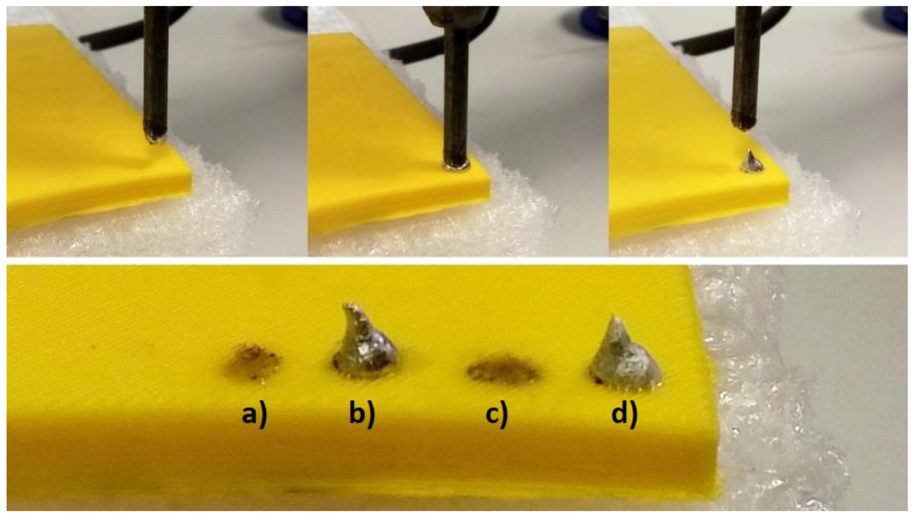
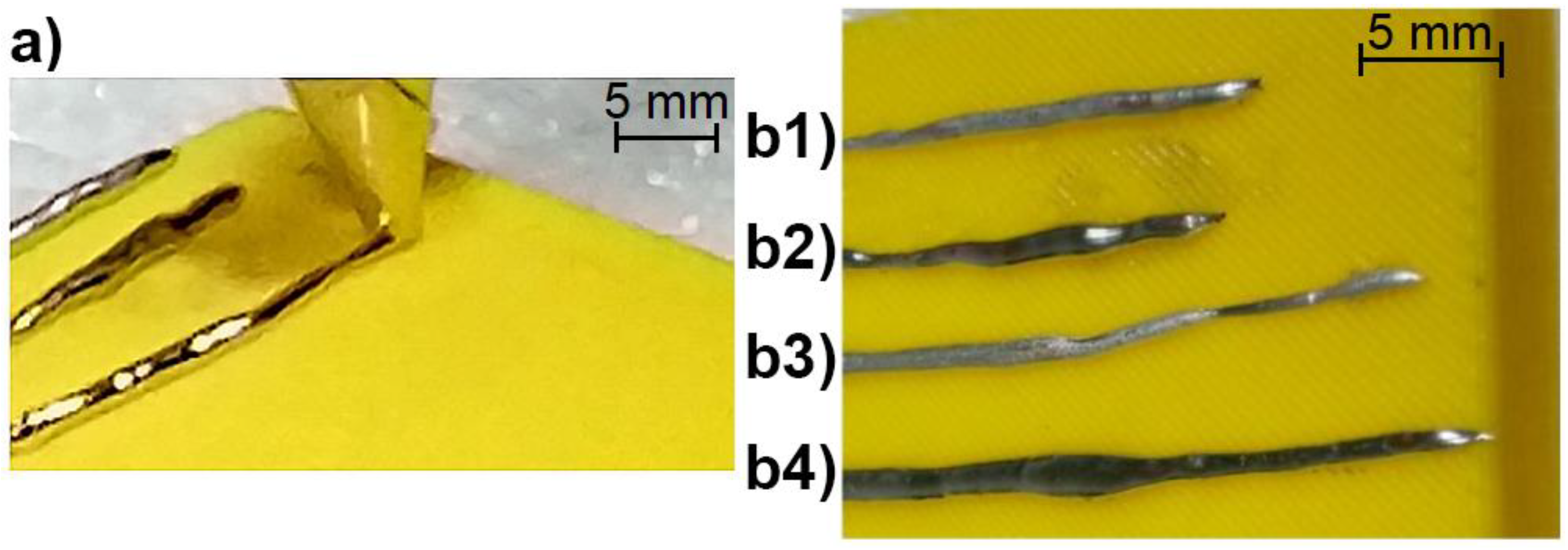
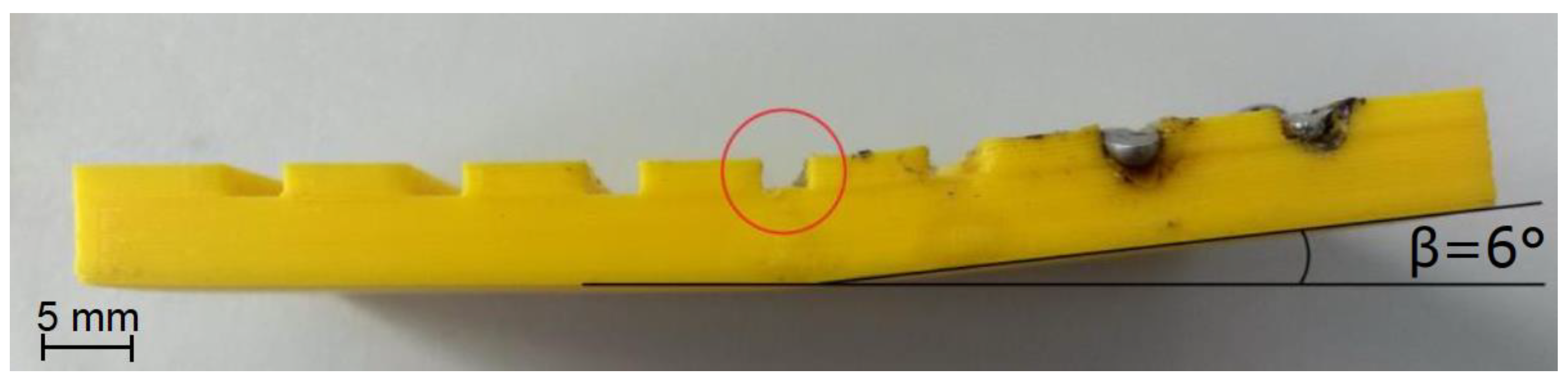
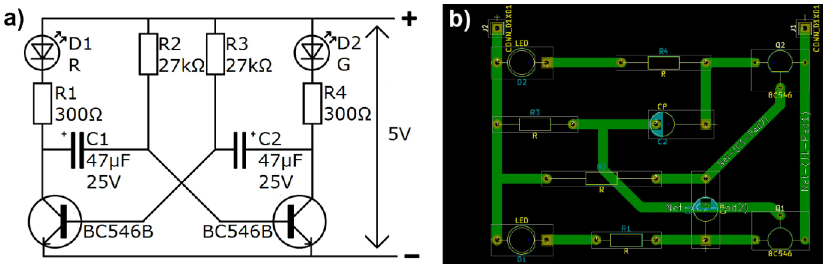
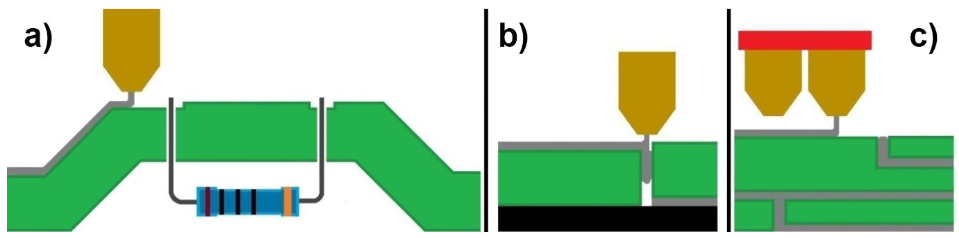
3. Results and Discussion
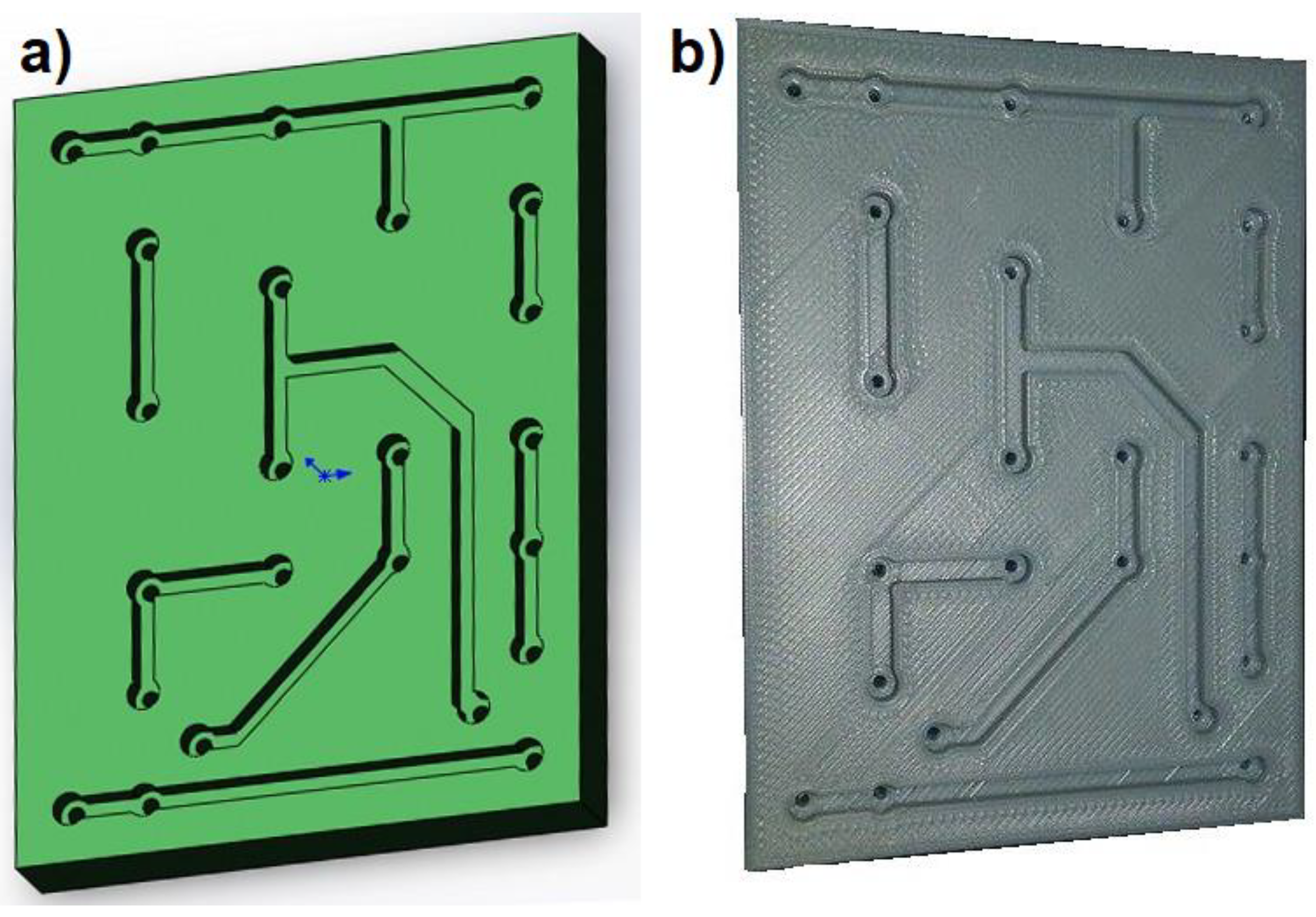
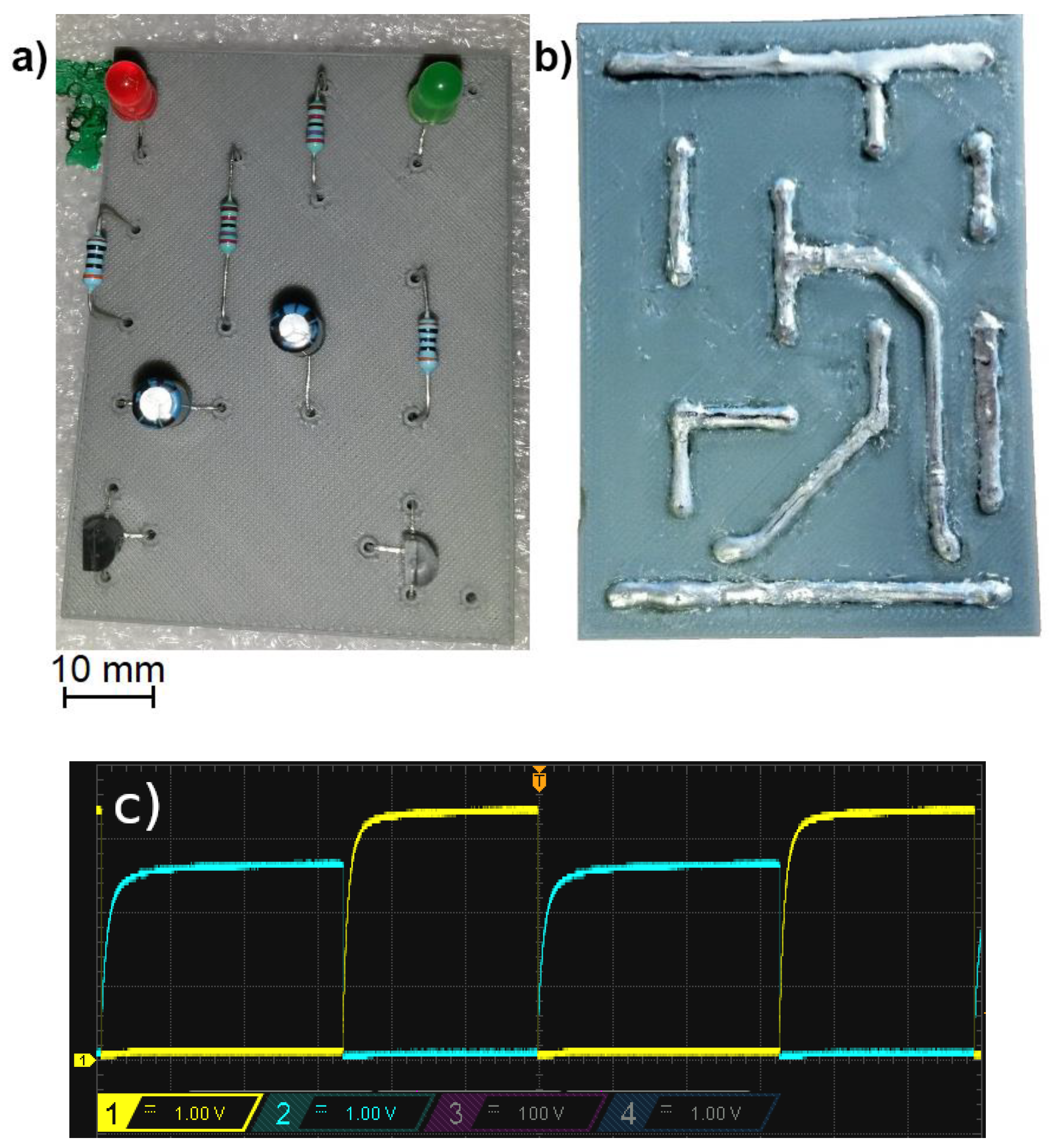
Determining whether the solder alloy exhibits adequate wettability and adhesion to the substrate is necessary to verify the possibility of fabricating metallic conductive paths on a polymer substrate. The first test of adhesion of the solder to the ABS substrate was evaluated by touching the substrate with a molten solder located on the soldering iron tip. It has been observed that the solder wires with the flux are problematic to adapt for this deposition technique. It has been noted that the polymer surface is covered by a thin flux layer, which significantly decreases the adhesion between the solder alloy and the polymer. On the other hand, solder without flux was applied to the substrate successfully. This allowed obtaining the first test metal deposition on the ABS substrates, as presented in Figure 2.
After rejecting the flux-containing solder wires, attempts were made to fabricate a long metal path on a polymer substrate. The alloys were deposited using a specially designed cone-shaped aluminum nozzle heated with a soldering iron or hot air to increase the homogeneity of the fabricated paths. The solder alloy is melted in the nozzle and freely deposited on the polymer substrate (Figure 3). The operating temperature of the soldering iron for both solder alloys (Sn60Pb40 and Sn99Ag0.3Cu0.7) is 285 °C. The research results confirmed the possibility of the additive application of solder alloys as conductive paths on a polymer substrate. The study also shows that the Sn60Pb40 solder is less viscous, possibly allowing for the deposit of longer paths.
The fabrication of paths using the above method has significant limitations. Conductive paths have nonuniform widths and a very limited length. Additionally, due to the poor wetting of the substrate, the obtained paths did not have a uniform thickness. To deal with the nonuniform thickness problem, we have proposed the deposition of the metal alloy into the specially prepared grooves (with triangular and rectangular cross-section shapes) fabricated on the 3D printed substrate. In both cases, we were able to obtain a uniform cross-section of the path along the entire length, resulting in repeatable resistance of the printed paths (Figure 4). In addition, this solution significantly increases the contact surface between the solder and the polymer. This results in increased adhesion between materials, therefore, the problem of solder pealing from the polymer surface is minimized.
During the study, it was noted that a single application of a liquid solder alloy on the ABS surface shows no significant effect on the properties of the plastic at the application point, as the required melting points of the alloys are lower than the melting point of the ABS plastic. The same phenomenon was observed in our previous studies, where we successfully obtained conductive paths with laser-sintered silver paths on polymer substrates [67]. However, after making paths in the same groove several times, a bending of the substrate was observed at the solder alloy application place (Figure 5). The high temperature of the fused solder can negatively affect the polymer substrate if the deposition speed is too slow or the process is repeated several times. This is due to the thermal shock resulting from the temperature gradient between the upper (heated) and bottom (non-heated) parts of the 3D printed substrate. The solution for such a problem can be a heated table or heated chamber of the 3D printer. The angle of the bending increases with the subsequent application of liquid solder.

4. Demonstrator

The symmetrical astable multivibrator circuit based on bipolar junction transistors (BJT) was fabricated to demonstrate the possibility of simultaneous production of conductive tracks and through-hole mountings with this additive method. While research has shown that it is possible to fabricate conductive metallic paths using the proposed FDMm technology on polymer substrates to make a fully functional electrical circuit, it is also necessary to perform the assembly of electronic components. For this purpose, the design of a multivibrator circuit containing electronic components, such as resistors, capacitors, transistors, and LEDs, was created. The circuit design was created in CAE (computer-aided engineering) software (Figure 6). The width of the conductive paths was set to 2 mm to 3D print grooves in the polymer substrate efficiently.
In the first stage of electrical circuit fabrication, an ABS substrate was printed on a standard FDM printer along with grooves (2 mm in width and height, respectively) for metallic conductive paths and holes for THT (through-hole technology) component leads (Figure 7). The preparation of the conductive paths and assembly of the THT elements took place in one process by filling the grooves with solder alloy using an aluminum nozzle and hot air soldering iron. The surface of the grooves was thoroughly cleaned with an organic solvent, and the soldering flux was applied only on the leads of the electronic components.
The Sn99Ag0.3Cu0.7 solder alloy was used to manufacture a functional multivibrator circuit, as presented in Figure 8a,b. A short video demonstrating the electrical circuit operation can be found in “Supplementary Materials”, along with the voltage plot illustrating the output waveform for Q and Q ¯ outputs of the multivibrator for the supply voltage of 5 V (Figure 8c). The difference in the voltage value can be attributed to the variations in path and contact resistance for the separate channels in the circuit and should be improved for higher-performance circuits.

5. Future Perspectives

This method’s attractive feature lies in its ability to directly print out a low-viscosity molten alloy at room temperature into arbitrary solidified 3D shapes. The method and results presented can be extended to develop the other forming approach in AM technologies to build 3D metal macrostructures, which can serve as a guide for printing other fusible alloys with low viscosity and high surface tension for a wide range of applications. Furthermore, future work can be extended to build multimaterial and multifunctional devices composed of metal and nonmetal materials together by extruding them out of multiple nozzles simultaneously.
Research should be continued to develop the deposition method of solder alloys on complex, three-dimensionally shaped polymer substrates (Figure 9a). It is necessary to investigate the possibility of depositing solders on sloping surfaces while maintaining their high quality and adhesion to the substrate. Another example of the direction of development in circuit manufacturing is double and multilayer electrical boards. In the case of double-layer circuits, it is necessary to study the possibility of filling the vias with solder alloy (Figure 9b). In the case of multilayer circuits, apart from the necessity to produce vias with solder, it is also necessary to develop appropriate printing parameters, which differ significantly in the case of polymer and solder deposition (Figure 9c).

6. Conclusions

This research evaluated the possibility of manufacturing durable electrical connections on an ABS plastic substrate by additive manufacturing. The paper describes how to produce metallic paths manually, but the process would be carried out analogously for a fully automated process. This makes it relatively easy to design a print nozzle for a standard FDM printer along the lines outlined to enable metallic tracks to be applied in an automated process. The presented metal deposition technique allows the simultaneous fabrication of polymer substrates and metal paths in one process with one printer. Thanks to the characteristic feature of the FDM technology, which produces an element layer by layer, using a multinozzle machine equipped with a nozzle for the deposition of the melted metal, it is possible to make multilayer electrical circuits in an automated way. The fabricated solder alloy paths also allow the electrical circuits to be efficiently completed with SMD components by soldering them. Equally important is the fact that the developed conductive paths consist entirely of metal and, therefore, have excellent electrical conductivity. Such high electrical conductivity is not possible in composites that can be used in standard FDM printing. This study focuses on one polymer and two solder alloys and shows their compatibility, considering wettability, adhesion, and thermal properties. For further studies, FDMm technology limitations need to be taken into account. The most significant disadvantage of this solution is that fabricating high-resolution paths is problematic. The diameter of the printing nozzle limits the minimum width of the printed path. This diameter must not be too small, as this will cause clogging in the print nozzle. At the same time, it needs to be small enough to manufacture connections for certain types of integrated circuits, such as BGA, flip-chip, or high-density QFP. The ABS polymer substrate used in the presented studies has inferior mechanical properties compared to the standard and most widely used substrate for manufacturing printed circuit boards—FR-4 laminate.

Supplementary Materials

The following supporting information can be found at Supplementary Material S1: Video of a working, symmetrical, astable multivibrator circuit fabricated with FDMm technology—http://www.weles.info/FDMm.mp4.

Author Contributions

Conceptualization, M.S. and L.B.; methodology, M.S. and L.B.; validation, M.S. and B.P.; formal analysis, M.S.; investigation, L.B.; resources, M.S.; writing—original draft preparation, B.P. and L.B.; writing—review and editing, B.P. and M.S.; visualization, L.B.; supervision, M.S.; project administration, M.S.; funding acquisition, M.S. All authors have read and agreed to the published version of the manuscript.

Funding

This research is supported by the Foundation for Polish Science, within the project “Functional heterophase materials for structural electronics” (First TEAM/2016-1/7), and co-financed by the European Union under the European Regional Development Fund.

Data Availability Statement

The data presented in this study are available upon request from the corresponding author.

Acknowledgments

This research was supported by the Institute of Metrology and Biomedical Engineering (Faculty of Mechatronics at the Warsaw University of Technology).

Conflicts of Interest

The authors declare no conflict of interest.

References

  1. Bloomberg.com. The Bridge to Smart Technology. 2009. Available online: https://www.bloomberg.com/news/articles/2009-02-18/the-bridge-to-smart-technology (accessed on 10 October 2022).
  2. DuPont and TactoTek Collaborate to Support Growing In-Mold Electronics Market. Available online: https://tactotek.com/media/news/dupont-and-tactotek-collaborate-to-support-growing-in-mold-electronics-market/ (accessed on 10 October 2022).
  3. Wearable Technology 2015–2025: Technologies, Markets, Forecasts. 2015. Available online: https://www.idtechex.com/en/research-report/wearable-technology-2015-2025-technologies-markets-forecasts/427 (accessed on 10 October 2022).
  4. Gibson, I.; Rosen, D.; Stucker, B. Additive Manufacturing Technologies: 3D Printing, Rapid Prototyping, and Direct Digital Manufacturing, 2nd ed.; Springer-Verlag: New York, NY, USA, 2015; ISBN 978-1-4939-4455-2. [Google Scholar]
  5. Mueller, B. Additive Manufacturing Technologies—Rapid Prototyping to Direct Digital Manufacturing. Assem. Autom. 2012, 32. [Google Scholar] [CrossRef]
  6. Upcraft, S.; Fletcher, R. The Rapid Prototyping Technologies. Assem. Autom. 2003, 23, 318–330. [Google Scholar] [CrossRef]
  7. Williams, J.M.; Adewunmi, A.; Schek, R.M.; Flanagan, C.L.; Krebsbach, P.H.; Feinberg, S.E.; Hollister, S.J.; Das, S. Bone Tissue Engineering Using Polycaprolactone Scaffolds Fabricated via Selective Laser Sintering. Biomaterials 2005, 26, 4817–4827. [Google Scholar] [CrossRef]
  8. Gaytan, S.M.; Murr, L.E.; Medina, F.; Martinez, E.; Lopez, M.I.; Wicker, R.B. Advanced Metal Powder Based Manufacturing of Complex Components by Electron Beam Melting. Mater. Technol. 2009, 24, 180–190. [Google Scholar] [CrossRef]
  9. Lee, M.P.; Cooper, G.J.T.; Hinkley, T.; Gibson, G.M.; Padgett, M.J.; Cronin, L. Development of a 3D Printer Using Scanning Projection Stereolithography. Sci. Rep. 2015, 5, 9875. [Google Scholar] [CrossRef] [PubMed] [Green Version]
  10. Zein, I.; Hutmacher, D.W.; Tan, K.C.; Teoh, S.H. Fused Deposition Modeling of Novel Scaffold Architectures for Tissue Engineering Applications. Biomaterials 2002, 23, 1169–1185. [Google Scholar] [CrossRef]
  11. Goh, G.D.; Yap, Y.L.; Tan, H.K.J.; Sing, S.L.; Goh, G.L.; Yeong, W.Y. Process–Structure–Properties in Polymer Additive Manufacturing via Material Extrusion: A Review. Crit. Rev. Solid State Mater. Sci. 2020, 45, 113–133. [Google Scholar] [CrossRef]
  12. Lakhdar, Y.; Tuck, C.; Binner, J.; Terry, A.; Goodridge, R. Additive Manufacturing of Advanced Ceramic Materials. Prog. Mater. Sci. 2021, 116, 100736. [Google Scholar] [CrossRef]
  13. Yakout, M.; Elbestawi, M.A.; Veldhuis, S.C. A Review of Metal Additive Manufacturing Technologies. Solid State Phenom. 2018, 278, 1–14. [Google Scholar] [CrossRef]
  14. Le-Bail, A.; Maniglia, B.C.; Le-Bail, P. Recent Advances and Future Perspective in Additive Manufacturing of Foods Based on 3D Printing. Curr. Opin. Food Sci. 2020, 35, 54–64. [Google Scholar] [CrossRef]
  15. Javaid, M.; Haleem, A. 3D Printed Tissue and Organ Using Additive Manufacturing: An Overview. Clin. Epidemiol. Glob. Health 2020, 8, 586–594. [Google Scholar] [CrossRef] [Green Version]
  16. Yoshida, H.; Igarashi, T.; Obuchi, Y.; Takami, Y.; Sato, J.; Araki, M.; Miki, M.; Nagata, K.; Sakai, K.; Igarashi, S. Architecture-Scale Human-Assisted Additive Manufacturing. ACM Trans. Graph. 2015, 34, 88. [Google Scholar] [CrossRef]
  17. Moon, S.K.; Tan, Y.E.; Hwang, J.; Yoon, Y.-J. Application of 3D Printing Technology for Designing Light-Weight Unmanned Aerial Vehicle Wing Structures. Int. J. Precis. Eng. Manuf. Green Techol. 2014, 1, 223–228. [Google Scholar] [CrossRef]
  18. Yap, Y.L.; Yeong, W.Y. Additive Manufacture of Fashion and Jewellery Products: A Mini Review. Virtual Phys. Prototyp. 2014, 9, 195–201. [Google Scholar] [CrossRef]
  19. Ventola, C.L. Medical Applications for 3D Printing: Current and Projected Uses. Pharm. Ther. 2014, 39, 704–711. [Google Scholar]
  20. Berman, B. 3-D Printing: The New Industrial Revolution. Bus. Horiz. 2012, 55, 155–162. [Google Scholar] [CrossRef]
  21. Yang, L.; Rida, A.; Vyas, R.; Tentzeris, M.M. RFID Tag and RF Structures on a Paper Substrate Using Inkjet-Printing Technology. IEEE Trans. Microw. Theory Technol. 2007, 55, 2894–2901. [Google Scholar] [CrossRef] [Green Version]
  22. Kopyt, P.; Salski, B.; Olszewska-Placha, M.; Janczak, D.; Sloma, M.; Kurkus, T.; Jakubowska, M.; Gwarek, W. Graphene-Based Dipole Antenna for a UHF RFID Tag. IEEE Trans. Antennas Propag. 2016, 64, 2862–2868. [Google Scholar] [CrossRef]
  23. Subramanian, V.; Chang, P.C.; Lee, J.B.; Molesa, S.E.; Volkman, S.K. Printed Organic Transistors for Ultra-Low-Cost RFID Applications. IEEE Trans. Compon. Packag. Technol. 2005, 28, 742–747. [Google Scholar] [CrossRef]
  24. Siuzdak, K.; Klein, M.; Sawczak, M.; Wróblewski, G.; Słoma, M.; Jakubowska, M.; Cenian, A. Spray-deposited carbon-nanotube counter-electrodes for dye-sensitized solar cells. Phys. Status Solidi A Appl. Mater. Sci. 2016, 213, 1157–1164. [Google Scholar] [CrossRef]
  25. Hoth, C.N.; Schilinsky, P.; Choulis, S.A.; Brabec, C.J. Printing Highly Efficient Organic Solar Cells. Nano Lett. 2008, 8, 2806–2813. [Google Scholar] [CrossRef]
  26. Jeong, J.-A.; Lee, J.; Kim, H.; Kim, H.-K.; Na, S.-I. Ink-Jet Printed Transparent Electrode Using Nano-Size Indium Tin Oxide Particles for Organic Photovoltaics. Sol. Energy Mater. Sol. Cells 2010, 94, 1840–1844. [Google Scholar] [CrossRef]
  27. Akhavan, V.A.; Goodfellow, B.W.; Panthani, M.G.; Steinhagen, C.; Harvey, T.B.; Stolle, C.J.; Korgel, B.A. Colloidal CIGS and CZTS Nanocrystals: A Precursor Route to Printed Photovoltaics. J. Solid State Chem. 2012, 189, 2–12. [Google Scholar] [CrossRef]
  28. Hart, J.P.; Wring, S.A. Recent Developments in the Design and Application of Screen-Printed Electrochemical Sensors for Biomedical, Environmental and Industrial Analyses. TrAC Trends Anal. Chem. 1997, 16, 89–103. [Google Scholar] [CrossRef]
  29. Wang, J.; Musameh, M. Carbon Nanotube Screen-Printed Electrochemical Sensors. Analyst 2004, 129, 1–2. [Google Scholar] [CrossRef]
  30. Honeychurch, K.C.; Hart, J.P. Screen-Printed Electrochemical Sensors for Monitoring Metal Pollutants. TrAC Trends Anal. Chem. 2003, 22, 456–469. [Google Scholar] [CrossRef]
  31. Sibinski, M.; Jakubowska, M.; Sloma, M. Flexible Temperature Sensors on Fibers. Sensors 2010, 10, 7934–7946. [Google Scholar] [CrossRef] [Green Version]
  32. Wood, V.; Halpert, J.E.; Panzer, M.J.; Bawendi, M.G.; Bulović, V. Alternating Current Driven Electroluminescence from ZnSe/ZnS:Mn/ZnS Nanocrystals. Nano Lett. 2009, 9, 2367–2371. [Google Scholar] [CrossRef]
  33. Słoma, M.; Wróblewski, G.; Janczak, D.; Jakubowska, M. Transparent Electrodes with Nanotubes and Graphene for Printed Optoelectronic Applications. J. Nanomater. 2014, 2014, 143094. [Google Scholar] [CrossRef] [Green Version]
  34. Sloma, M.; Janczak, D.; Wroblewski, G.; Mlozniak, A.; Jakubowska, M. Electroluminescent Structures Printed on Paper and Textile Elastic Substrates. Circuit World 2014, 40, 13–16. [Google Scholar] [CrossRef]
  35. Rizzo, A.; Mazzeo, M.; Biasiucci, M.; Cingolani, R.; Gigli, G. White Electroluminescence from a Microcontact-Printing-Deposited CdSe/ZnS Colloidal Quantum-Dot Monolayer. Small 2008, 4, 2143–2147. [Google Scholar] [CrossRef]
  36. Hilder, M.; Winther-Jensen, B.; Clark, N.B. Paper-Based, Printed Zinc–Air Battery. J. Power Sources 2009, 194, 1135–1141. [Google Scholar] [CrossRef]
  37. Braam, K.T.; Volkman, S.K.; Subramanian, V. Characterization and Optimization of a Printed, Primary Silver–Zinc Battery. J. Power Sources 2012, 199, 367–372. [Google Scholar] [CrossRef]
  38. Chen, P.; Chen, H.; Qiu, J.; Zhou, C. Inkjet Printing of Single-Walled Carbon Nanotube/RuO2 Nanowire Supercapacitors on Cloth Fabrics and Flexible Substrates. Nano Res. 2010, 3, 594–603. [Google Scholar] [CrossRef] [Green Version]
  39. Chen, T.; Xue, Y.; Roy, A.K.; Dai, L. Transparent and Stretchable High-Performance Supercapacitors Based on Wrinkled Graphene Electrodes. ACS Nano 2014, 8, 1039–1046. [Google Scholar] [CrossRef]
  40. Dighe, A.B.; Dubal, D.P.; Holze, R. Screen Printed Asymmetric Supercapacitors Based on LiCoO2 and Graphene Oxide*: Screen Printed Asymmetric Supercapacitors Based on LiCoO2. Z. Anorg. Allg. Chem. 2014, 640, 2852–2857. [Google Scholar] [CrossRef]
  41. Dul, S.; Fambri, L.; Pegoretti, A. Fused Deposition Modelling with ABS–Graphene Nanocomposites. Compos. Part A Appl. Sci. Manuf. 2016, 85, 181–191. [Google Scholar] [CrossRef]
  42. Yang, S.; Relations, M. 3D-Printed ‘Smart Cap’ Uses Electronics to Sense Spoiled Food. Available online: https://news.berkeley.edu/2015/07/20/3d-printed-electronic-smart-cap/ (accessed on 12 July 2021).
  43. Leigh, S.J.; Bradley, R.J.; Purssell, C.P.; Billson, D.R.; Hutchins, D.A. A Simple, Low-Cost Conductive Composite Material for 3D Printing of Electronic Sensors. PLoS ONE 2012, 7, e49365. [Google Scholar] [CrossRef] [PubMed]
  44. Dul, S.; Fambri, L.; Pegoretti, A. Filaments Production and Fused Deposition Modelling of ABS/Carbon Nanotubes Composites. Nanomaterials 2018, 8, 49. [Google Scholar] [CrossRef] [PubMed] [Green Version]
  45. Jakus, A.E.; Secor, E.B.; Rutz, A.L.; Jordan, S.W.; Hersam, M.C.; Shah, R.N. Three-Dimensional Printing of High-Content Graphene Scaffolds for Electronic and Biomedical Applications. ACS Nano 2015, 9, 4636–4648. [Google Scholar] [CrossRef]
  46. Muth, J.T.; Vogt, D.M.; Truby, R.L.; Mengüç, Y.; Kolesky, D.B.; Wood, R.J.; Lewis, J.A. Embedded 3D Printing of Strain Sensors within Highly Stretchable Elastomers. Adv. Mater. 2014, 26, 6307–6312. [Google Scholar] [CrossRef] [PubMed]
  47. Le, L.T.; Ervin, M.H.; Qiu, H.; Fuchs, B.E.; Lee, W.Y. Graphene Supercapacitor Electrodes Fabricated by Inkjet Printing and Thermal Reduction of Graphene Oxide. Electrochem. Commun. 2011, 13, 355–358. [Google Scholar] [CrossRef]
  48. Liu, B.; Wang, Y.; Lin, Z.; Zhang, T. Creating Metal Parts by Fused Deposition Modeling and Sintering. Mater. Lett. 2020, 263, 127252. [Google Scholar] [CrossRef]
  49. Podsiadły, B.; Skalski, A.; Wałpuski, B.; Słoma, M. Heterophase Materials for Fused Filament Fabrication of Structural Electronics. J. Mater. Sci. Mater. Electron. 2019, 30, 1236–1245. [Google Scholar] [CrossRef]
  50. First 3-D Printed Loudspeaker Hints at Future of Consumer Electronics—IEEE Spectrum. Available online: https://spectrum.ieee.org/tech-talk/consumer-electronics/gadgets/first-3d-printed-loudspeaker-hints-at-future-of-consumer-electronics (accessed on 10 October 2022).
  51. Wu, S.-Y.; Yang, C.; Hsu, W.; Lin, L. 3D-Printed Microelectronics for Integrated Circuitry and Passive Wireless Sensors. Microsyst. Nanoeng. 2015, 1, 15013. [Google Scholar] [CrossRef] [Green Version]
  52. Espalin, D.; Muse, D.W.; MacDonald, E.; Wicker, R.B. 3D Printing Multifunctionality: Structures with Electronics. Int. J. Adv. Manuf. Technol. 2014, 72, 963–978. [Google Scholar] [CrossRef]
  53. Walker, S.B.; Lewis, J.A. Reactive Silver Inks for Patterning High-Conductivity Features at Mild Temperatures. J. Am. Chem. Soc. 2012, 134, 1419–1421. [Google Scholar] [CrossRef]
  54. Khaing, M.W.; Fuh, J.Y.H.; Lu, L. Direct Metal Laser Sintering for Rapid Tooling: Processing and Characterisation of EOS Parts. J. Mater. Process. Technol. 2001, 113, 269–272. [Google Scholar] [CrossRef]
  55. Hinojos, A.; Mireles, J.; Reichardt, A.; Frigola, P.; Hosemann, P.; Murr, L.E.; Wicker, R.B. Joining of Inconel 718 and 316 Stainless Steel Using Electron Beam Melting Additive Manufacturing Technology. Mater. Des. 2016, 94, 17–27. [Google Scholar] [CrossRef] [Green Version]
  56. Wang, F.; Williams, S.; Colegrove, P.; Antonysamy, A.A. Microstructure and Mechanical Properties of Wire and Arc Additive Manufactured Ti-6Al-4V. Metall. Mater. Trans. A 2013, 44, 968–977. [Google Scholar] [CrossRef]
  57. Szost, B.A.; Terzi, S.; Martina, F.; Boisselier, D.; Prytuliak, A.; Pirling, T.; Hofmann, M.; Jarvis, D.J. A Comparative Study of Additive Manufacturing Techniques: Residual Stress and Microstructural Analysis of CLAD and WAAM Printed Ti–6Al–4V Components. Mater. Des. 2016, 89, 559–567. [Google Scholar] [CrossRef]
  58. Ding, D.; Pan, Z.; Cuiuri, D.; Li, H. Wire-Feed Additive Manufacturing of Metal Components: Technologies, Developments and Future Interests. Int. J. Adv. Manuf. Technol. 2015, 81, 465–481. [Google Scholar] [CrossRef]
  59. Ma, Y.; Cuiuri, D.; Hoye, N.; Li, H.; Pan, Z. Effects of Wire Feed Conditions on in Situ Alloying and Additive Layer Manufacturing of Titanium Aluminides Using Gas Tungsten Arc Welding. J. Mater. Res. 2014, 29, 2066–2071. [Google Scholar] [CrossRef]
  60. Fang, M.; Chandra, S.; Park, C.B. Building Three-dimensional Objects by Deposition of Molten Metal Droplets. Rapid Prototyp. J. 2008, 14, 44–52. [Google Scholar] [CrossRef]
  61. Yu, Y.; Liu, F.; Liu, J. Direct 3D Printing of Low Melting Point Alloy via Adhesion Mechanism. Rapid Prototyp. J. 2017, 23, 642–650. [Google Scholar] [CrossRef]
  62. Warrier, N.; Kate, K.H. Fused Filament Fabrication 3D Printing with Low-Melt Alloys. Prog. Addit. Manuf. 2018, 3, 51–63. [Google Scholar] [CrossRef]
  63. RepRap: Blog: First Reprapped Circuit. Available online: http://blog.reprap.org/2009/04/first-reprapped-circuit.html (accessed on 10 October 2022).
  64. Mireles, J.; Espalin, D.; Roberson, D.; Zinniel, B.; Medina, F.; Wicker, R. Fused Deposition Modeling of Metals; University of Texas at Austin: Austin, TX, USA, 2012. [Google Scholar] [CrossRef]
  65. Mireles, J.; Kim, H.-C.; Hwan Lee, I.; Espalin, D.; Medina, F.; MacDonald, E.; Wicker, R. Development of a Fused Deposition Modeling System for Low Melting Temperature Metal Alloys. J. Electron. Packag. 2013, 135, 011008. [Google Scholar] [CrossRef]
  66. Singh, N.; Singh, R. Conducting Polymer Solution and Gel Processing. In Reference Module in Materials Science and Materials Engineering; Elsevier: Amsterdam, The Netherlands, 2017; ISBN 978-0-12-803581-8. [Google Scholar]
  67. Wałpuski, B.; Słoma, M. Additive Manufacturing of Electronics from Silver Nanopowders Sintered on 3D Printed Low-Temperature Substrates. Adv. Eng. Mater. 2021, 23, 2001085. [Google Scholar] [CrossRef]
Figure 1. Schematic illustration of an additive process for fabricating 3D-printed structural circuits from fusible alloys. (a) Preparation of a polymer substrate with the standard FDM printing process using thermoplastic polymers or composites. (b) Fabrication of conductive metallic paths from fusible alloys with a modified FDM technique adapted for low-temperature metals and alloys (FDMm).
Electronics 11 03829 g001
Figure 2. Results of adhesion tests of solder alloys on an ABS surface: (a) Sn60Pb40 with flux; (b) Sn60Pb40 without flux; (c) Sn99Ag0.3Cu0.7 with flux; (d) Sn99Ag0.3Cu0.7 without flux.
Electronics 11 03829 g002
Figure 3. (a) Fabrication of conductive paths using a specially designed aluminum nozzle; Paths fabricated using: (b1) hot air and Sn99Ag0.3Cu0.7; (b2) hot air and Sn60Pb40; (b3) hot iron and Sn99Ag0.3Cu0.7; (b4) hot iron and Sn60Pb40.
Electronics 11 03829 g003
Figure 4. Conductive paths obtained using aluminum nozzle by filling grooves in ABS substrate with (a) Sn99Ag0.3Cu0.7 and (b) Sn60Pb40 solder alloy.
Electronics 11 03829 g004
Figure 5. Deformation of the substrate as a result of thermal shock from applied liquid solder alloy 7 times in the same groove (red circle).
Electronics 11 03829 g005
Figure 6. (a) Electrical diagram of the symmetrical, astable multivibrator; (b) printed circuit board layout.
Electronics 11 03829 g006
Figure 7. (a) Polymer substrate visualization. (b) Resulted 3D printed polymer substrate.
Electronics 11 03829 g007
Figure 8. The 3D printed circuit after filling the grooves with Sn99Ag0.3Cu0.7 solder alloy: (a) top view (b) bottom view. (c) Output waveform for Q and Q ¯ outputs of the multivibrator.
Electronics 11 03829 g008
Figure 9. Schematic illustration of FDMm process: (a) on curved, 3D shaped substrate; (b) for double layer circuit board; (c) for multilayer circuit board.
Electronics 11 03829 g009
Publisher’s Note: MDPI stays neutral with regard to jurisdictional claims in published maps and institutional affiliations.

