Communication

HfOx/Ge RRAM with High ON/OFF Ratio and Good Endurance

1
China Nanhu Academy of Electronics and Information Technology, Jiaxing 314001, China
2
College of Information Science and Electronic Engineering, Zhejiang University, Hangzhou 310058, China
3
School of Integrated Circuits, East China Normal University, Shanghai 200241, China
*
Author to whom correspondence should be addressed.
Electronics 2022, 11(22), 3820; https://doi.org/10.3390/electronics11223820
Submission received: 24 October 2022 / Revised: 9 November 2022 / Accepted: 15 November 2022 / Published: 20 November 2022
(This article belongs to the Special Issue Advanced CMOS Devices and Applications)

Abstract

:
A trade-off between the memory window and the endurance exists for transition-metal-oxide RRAM. In this work, we demonstrated that HfOx/Ge-based metal-insulator-semiconductor RRAM devices possess both a larger memory window and longer endurance compared with metal-insulator-metal (MIM) RRAM devices. Under DC cycling, HfOx/Ge devices exhibit a 100× larger memory window compared to HfOx MIM devices, and a DC sweep of up to 20,000 cycles was achieved with the devices. The devices also realize low static power down to 1 nW as FPGA’s pull-up/pull-down resistors. Thus, HfOx/Ge devices act as a promising candidates for various applications such as FPGA or compute-in-memory, in which both a high ON/OFF ratio and decent endurance are required.

1. Introduction

Resistive random access memory (RRAM) has been intensively investigated for its diversified applications, including embedded memory, storage class memory, FPGA, and in-memory computation of neural networks [1,2,3]. Metal Oxide (i.e., HfOx, TaOx, NiO, and TiO2) is commonly applied as the switching layer sandwiched between two metal electrodes to build a metal-insulator-metal (MIM) structure. Among various switching layer materials, hafnium oxide (HfOx) stands out owing to its technical maturity, fab-friendliness, and decent device performance [4,5,6]. The choice of metal electrodes affects the behavior of HfOx-based RRAM a lot. Normally, when noble metal (i.e., Pt and Ru) is constructed as the top and bottom electrodes [7,8,9], the devices have unipolar switching because the conductive filament (CF) is annihilated by thermal diffusion. However, the switching behavior of unipolar RRAM is unstable, and the current during the annihilation of CF is too large for the applications of embedded memory, FPGA, and in-memory computation. As for bipolar RRAM, the materials of the top electrode are usually Ti, W, Al, and TiN [4,10,11,12,13,14,15]. Table 1 shows the benchmark of bipolar HfOx-based RRAM with different electrodes. It is reported that the endurance is 106~107 in reference [11,14], but the memory window (i.e., the ratio between high and low resistance states) is ~10. Reference [12] improved endurance to 1010 by utilizing oxygen plasma treatment within Ti/HfO2/TiN structured RRAM, while the memory window is 102 and the operation voltage is larger than 3 V. Moreover, reference [10] realized a larger memory window up to 105 as the thickness of HfO2 is 24.7 nm. It is observed that endurance can be improved by increasing the extra available oxygen ions in HfO2, and the memory window can be enlarged using a thicker HfO2 film. Nevertheless, both a large memory window and long endurance achieved in one RRAM device are difficult when the HfO2 film is less than 10 nm. In other words, there is generally a trade-off between the memory window and the endurance of MIM RRAM [16].
As of today, MIM-based HfOx RRAM is gradually entering the market at 40 nm technology nodes and beyond in embedded or standalone memory applications [17,18]. For advanced applications such as FPGA’s pull-up/pull-down resistors [19], or compute-in-memory (CIM) [20], both a low leakage in the high resistance state (HRS) and a large memory window are required to achieve good energy efficiency. Since MIM RRAMs with the HfOx switching layer often exhibit modest memory windows, an alternative stack with a higher ON/OFF ratio is highly desired. In this work, we experimentally studied the metal-insulator-semiconductor (MIS) RRAM devices with the HfOx switching layer and Ge or Si bottom electrodes in order to achieve a higher memory window with good endurance. In particular, a memory window over 105 was achieved with Pd/HfOx/p-Ge RRAM devices, and the conductance mechanism was analyzed in detail. Furthermore, stable DC cycles with a large memory window were demonstrated for Pd/HfOx/p-Ge devices up to 20,000 DC sweep cycles. Compared with TiN/HfOx/Pt devices and Pd/HfOx/p+-Si devices, Pd/HfOx/p-Ge devices possess better DC endurance under the same test condition. These results suggest HfOx/Ge RRAM device is a promising candidate for FPGA and CIM applications.

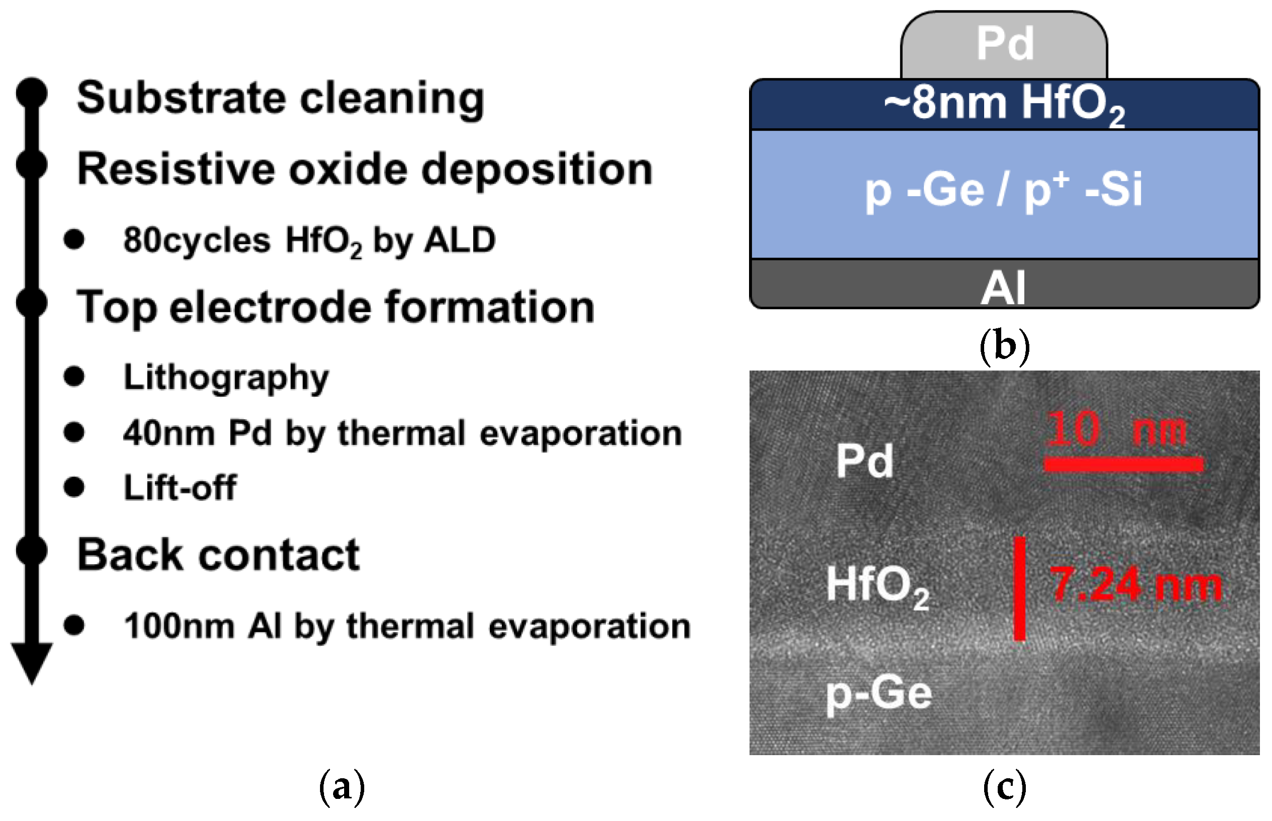
2. Materials and Methods

Two types of devices were fabricated, including MIS and MIM devices. For MIS devices, Pd/HfOx/p-Ge devices and Pd/HfOx/p+-Si devices were fabricated. The process flow is depicted in Figure 1a. After the wafer cleaning, 7 nm HfOx was deposited on Ge or Si substrates by Atomic Layer Deposition (ALD). The ozone post oxidation (OPO) is not processed here in contrast with the process of previous HfOx/Ge RRAM [21,22]. It is not only because the interface is vital for previous RRAM stack used in MOSFET, but the stack variable here needs to be the same as the one in MIM devices. Subsequently, the lithography process and Pd deposition were carried out, and a lift-off process was utilized to form the top electrode. Al was finally deposited using thermal evaporation as a contact metal to Ge or Si substrates. To distinguish the Ge-based and Si-based devices, hereinafter MIGe is used to refer Pd/HfOx/p-Ge devices, and MISi is used to refer Pd/HfOx/p+-Si devices. For MIM devices, a typical TiN/HfOx/Pt device was fabricated by the following process flow. First, back electrode Pt was sputtered on a SiO2 substrate. Next, 7 nm HfOx as the switching layer and 15 nm TiN as the top electrode were sequentially deposited by ALD. Afterward, the contact metal W was deposited by sputtering and patterned by lithography. Lastly, a W/TiN/HfOx stack was etched layer by layer using Inductive Coupled Plasma (ICP) tool to expose the bottom electrode.
The DC I-V characterizations were carried out by Agilent B1500A semiconductor parameter analyzer. SET and RESET operations were achieved by sweeping from a non-zero voltage Vstart to a larger voltage Vend, where Vend was large enough to trigger the switching event. During the SET operation, current compliance (CC) was exerted by B1500A on MIGe/MISi devices (CC = 50 μA) and MIM devices (CC = 1 mA). The READ operations were achieved by applying single-point voltage on the device and measuring the currents for resistance calculation.

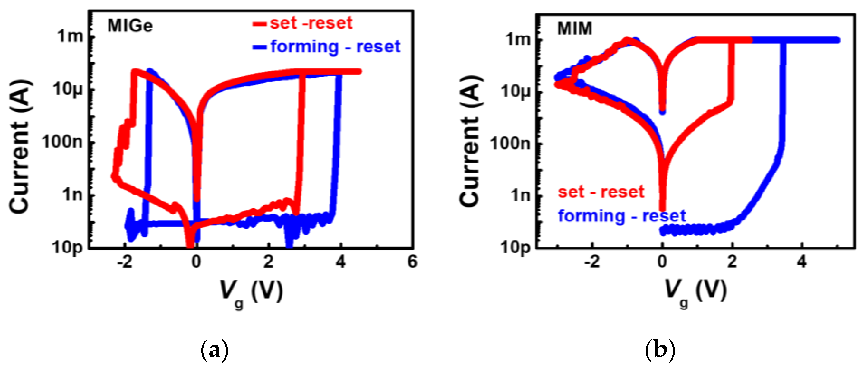
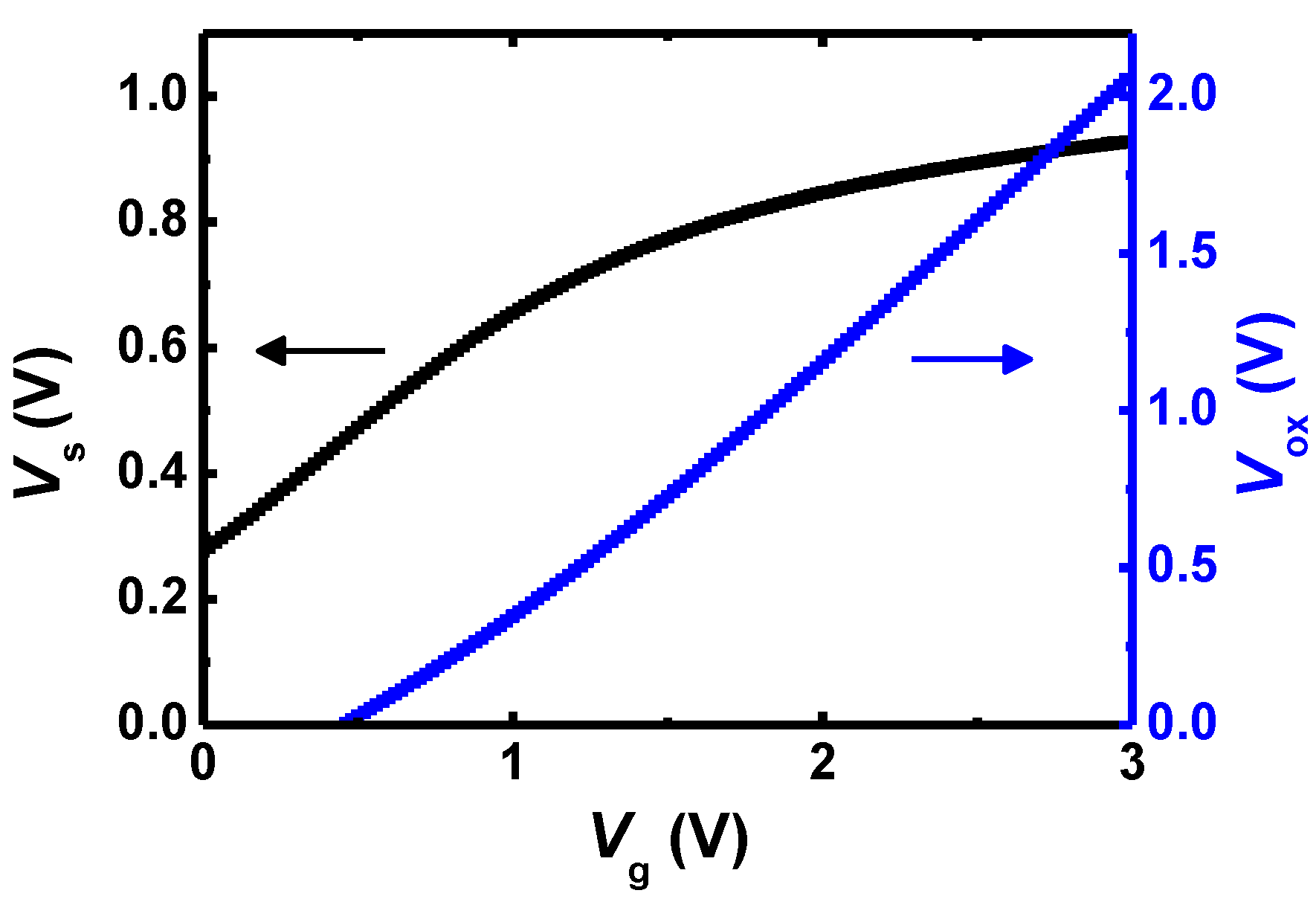
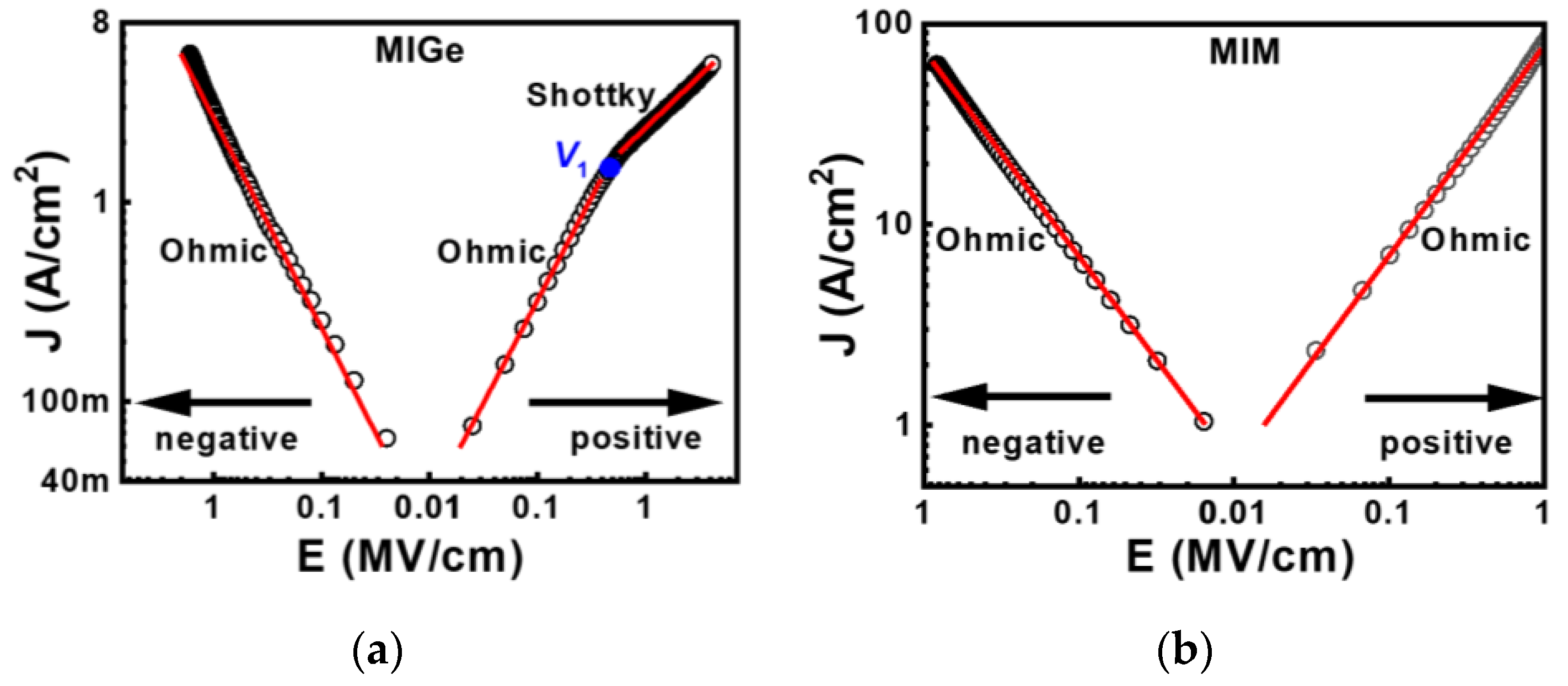
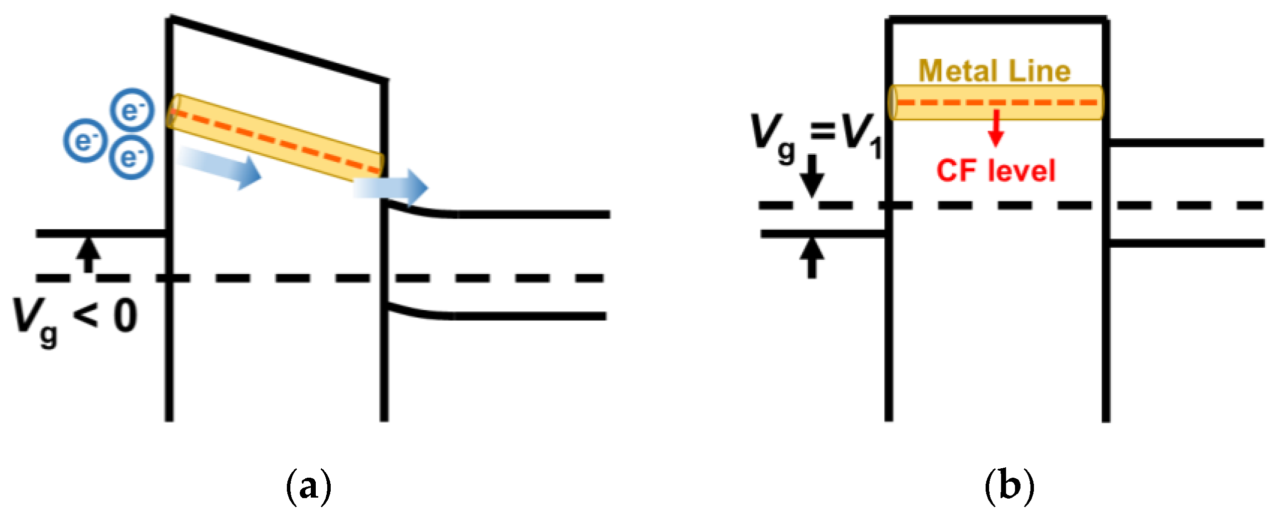
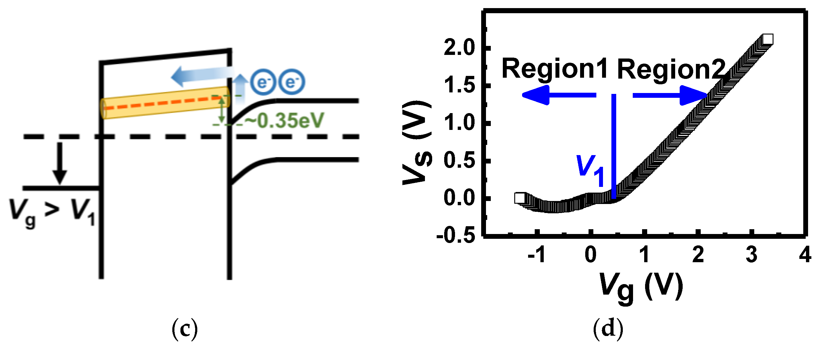
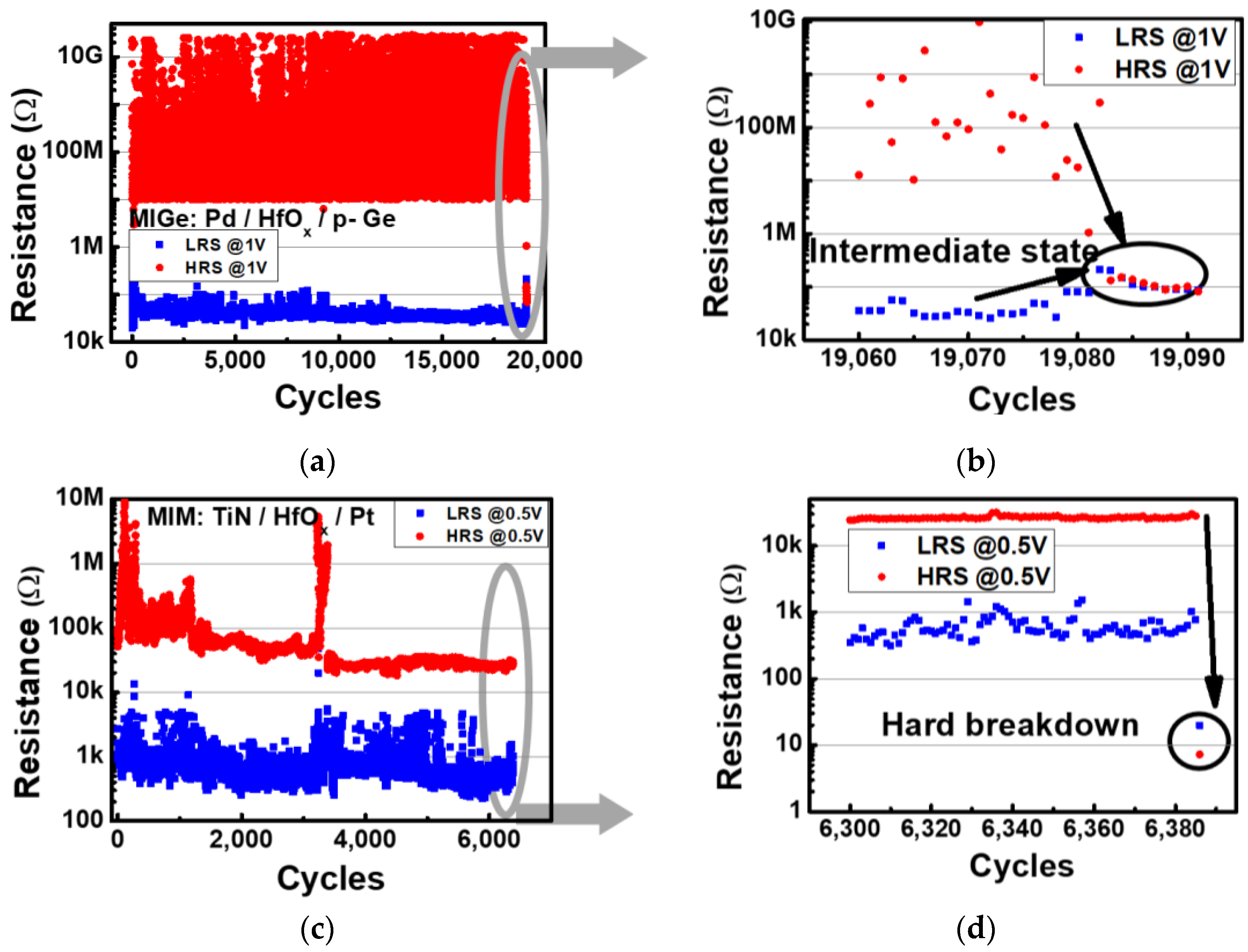
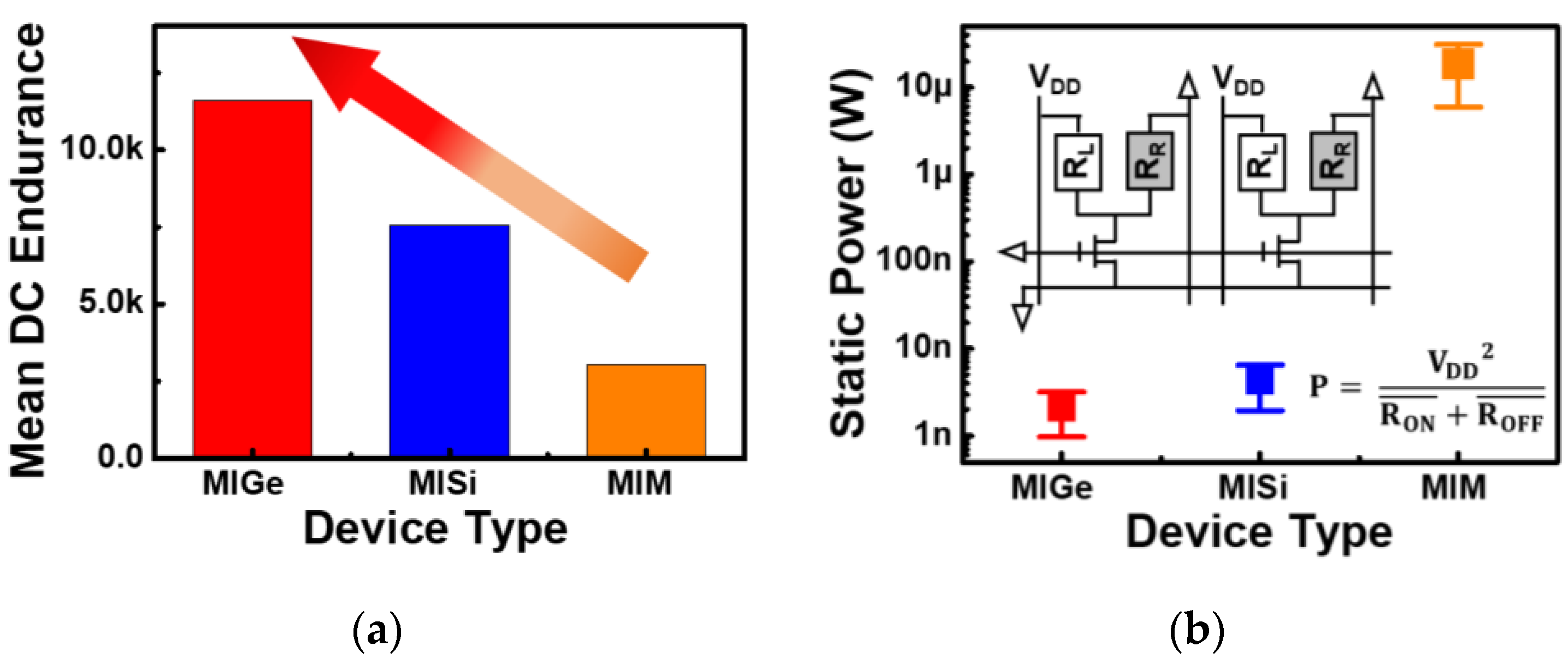
3. Results and Discussion

Typical DC I-V characteristics were measured for Pd/HfOx/p-Ge and TiN/HfOx/Pt devices, as shown in Figure 2. For MIM devices, stable low resistance states (LRS) can be achieved by 1 mA CC, and the resistance of high resistance states (HRS) is roughly 104 times the virgin-state resistance. The memory window of MIM devices is around 103, while a larger memory window of over 105 is realized in MIGe devices. It is worth noting that the HRS current of MIGe devices is approximately equal to the current of virgin states, implying a complete annihilation of the conductive filament (CF). Furthermore, the low operation current of MIGe (CC = 50 μA) leads to the advantage of low operating power. The RESET current of MIM devices is around several mA while that of MIGe devices is around 100 μA, in line with the SET current compliance. Thus, the write power of MIGe devices is estimated to be dozens of times smaller than that of MIM devices. For MIM devices, if a lower CC is applied to reduce the operation power, the memory window will also shrink significantly.
It is worth pointing out that the effective voltage drops on the oxide stack (Vox) of MIGe devices are less than the voltage applied on the gate/top electrode (Vg). There are two situations: (a) The MIGe device works like a MOS when it is at HRS due to the negligible CF; (b) When the MIGe device works at LRS, the CF is conductive, so the device is not equivalent to a MOS. In the case of HRS, the voltage on the gate contributes to a series of oxide capacitance (Cox) and substrate capacitance (Cs). The total capacitance (Ctot) is approximate to oxide capacitance at negative bias; thus, the voltage drop on the oxide stack is equal to Vg. While the device is positively biased, the surface potential, which is equal to the voltage dropped on the substrate (Vs), is extracted using a quasi-static technique [23,24]. The surface potential is expressed as Equation (1):
φ s ( V g ) = V acc V g [ 1 C ( V g ) C ox ] d V g + Δ
where, Δ is correction factor and expressed as:
Δ = V acc V FB [ 1 C ( V g ) C ox ] d V g
To obtain VFB, CFB needs to be calculated firstly using Equation (3):
C FB = 1 1 C ox + 1 C s ,     C s = ε s ε 0 D deby = ε s ε 0 k T ε s ε 0 / q 2 N A
NA is 5 × 10¹⁶ /cm3, and ε s is the relative permittivity of Germanium. Derived from Equation (1), the voltage across the RRAM stack and substrate varies with the gate voltage, as plotted in Figure 3. It is indicated that the practical voltage across the RRAM stack is the same as what is in MIM RRAM. Moreover, the substrate doping concentration does not affect the switching behavior except for the operation voltage due to the partial voltage on the substrate. Hence, the scalability will not be affected by the substrate doping concentration. As for the LRS state, the voltage across the RRAM stack and the substrate will be discussed further in this paper.
To further understand the conduction mechanisms of MIGe devices, double logarithmic J-E curves in LRS were plotted. As shown in Figure 4a, the fitting results suggest that two different conductive mechanisms exist for MIGe devices. When the applied voltage on the top electrode (TE) is less than V1, the conduction behavior is ohmic because ln(J) is proportional to ln(E), and the slope is around 1. When the voltage on the TE increases above V1, the slope of the curve reduces to smaller than 1. The current density vs. electric field data fits well with the Schottky emission equation in which ln(J) ∝ E1/2 [25]. Based on the Schottky emission equation, the barrier height ΦB is calculated to be 0.35 eV, while the electron effective mass in HfOx is approximated to be about 0.11 m0 [26]. The conductive current through CF is contributed by electrons, which are the minority carriers for MIGe devices. A comparatively low current through CF, especially at the moment of CF forming, could help limit the overgrowth of the CF region [27]. For MIM devices, the J-E curve is symmetric, as shown in Figure 4b, and the slopes are both around 1. Plenty of free electrons are available from the two metal electrodes leading to a high operating current.
Figure 5 exhibits the energy band diagram for the illustration of electronic transport mechanisms when the MIGe device works at HRS. As shown in Figure 5d, the voltage drop, Vg, is divided between the oxide switching layer and Ge substrate. When negatively biased, the resistance of the Ge substrate is negligible, and the resistance of CF (RCF) can be extracted from I-Vg. Then the voltage dropped on the Ge substrate (Vs) could be derived as VgI*RCF, where I*RCF is approximately the voltage on the switching oxide (Vox). Therefore, Vg is almost equal to Vox when the device is negatively biased (Vg < 0). On the other hand, when Vg > V1, Vg is mostly distributed to Vs. As depicted in Figure 5b, the conductive filament consists of abundant oxygen vacancies (VO), which can gather to form a quasi-continuous defect energy band in the bandgap of HfOx [28]. In this case, the filament consisting of VO can be treated as a metallic conducting path between the TE and Ge substrate at negative biases (Figure 5a). However, when the Vg is positive and larger than V1, the electrons from the Ge substrate need to overcome an energy barrier of 0.35 eV to reach the defect levels of the CF (Figure 5c). From the experimental data, it is estimated that the energy level of CF is close to the conduction band minimum (CBM) of Ge and roughly 1.75 eV below the CBM of HfO2. This energy level is consistent with previous studies, which identified VO levels to be ranging from 1.2 to 2.1 eV below the CBM of HfO2 [29,30,31].
Furthermore, the DC endurance was characterized for Pd/HfOx/p-Ge, Pd/HfOx/p+-Si, and TiN/HfOx/Pt devices. The sequence of SET-READ-RESET-READ cycles was used, and devices with the same dimension (40 μm × 40 μm) were characterized. The cycling results of MIGe and MIM devices were plotted in Figure 6, which suggests different endurance failure phenomena of MIGe and MIM devices. For MIM devices, it can be observed that a sudden hard breakdown happened during the RESET, as shown in Figure 6d. Its endurance failure behavior is similar to those that originated from the depletion of O2− which induced the RESET difficulty and increased vacancy concentrations [19,32]. In contrast, the MIGe devices maintained a stable endurance window of 100× or more but failed when the HRS and LRS converged into an intermediate state, as shown in Figure 6a,b. Although the distribution of HRS appears to be wide on account of the randomness of oxygen ion movement, pulse programming is an effective approach to improve the uniformity of HRS [10]. Pulse characterizations were implemented further for MIGe and MIM devices (data not shown here). The results of pulse endurance are in correspondence with the results of DC endurance. The MIGe device is still functional after 105 fully successful switching cycles, whereas the MIM device broke down after 104 pulse switching cycles. The effective operation cycles of the MIGe device (>105) are sufficient for CIM [33] since the SET/RESET operations will not be executed frequently.
In addition to the larger and more stable memory window achieved by MIGe devices, it is also demonstrated that the devices have superior endurance over the other two types of devices. To further confirm the superior endurance performance of MIGe devices compared to MISi and MIM, DC endurance tests were further carried out for multiple devices of each sample. Figure 7a summarizes the mean DC endurance of MIGe, MISi, and MIM devices. The mean DC endurance of MIGe devices is around 104, while that of MIM devices is ten times smaller. Moreover, the static power of FPGA’s pull-up/pull-down resistors when implemented with RRAM was calculated [2]. For FPGA’s configuration memory, the 1T2R structure was widely investigated. In these two resistors, usually one is ON, and the other is OFF. Therefore, the static power mainly depends on the OFF state resistor. Figure 7b compares the static powers of MIGe, MISi, and MIM devices at a 1.8 V supply. The results suggest that MIGe RRAM is a promising candidate for FPGA’s pull-up/pull-down resistors.

4. Conclusions

In conclusion, a large memory window of over 105 was demonstrated for Pd/HfOx/p-Ge RRAM devices. Furthermore, the devices have been proven to have better endurance and a more stable memory window than MISi and MIM RRAM devices. Moreover, a low static power down to 1 nW was observed in MIGe devices as FPGA’s pull-up/pull-down resistors. Therefore, HfOx/p-Ge-based RRAM is a promising candidate for FPGA applications.

Author Contributions

Conceptualization, N.W.; methodology, N.W.; software, N.W.; validation, N.W. and X.D.; formal analysis, N.W., X.D., S.G., W.W. and Y.Z.; investigation, N.W.; resources, W.W. and Y.Z.; data curation, N.W.; writing—original draft preparation, N.W.; writing—review and editing, N.W., X.D., S.G., W.W. and Y.Z.; visualization, N.W.; supervision, W.W. and Y.Z.; project administration, W.W. All authors have read and agreed to the published version of the manuscript.

Funding

This research was supported in part by the Zhejiang Province Natural Science Foundation of China under Grant LZ19F040001, National Key Research and Development Program of China under Grant 2020AAA0109001, Key Research and Development Program of Zhejiang Province under Grant 2021C01039, and the “Ling Yan” Program for Tackling Key Problems of Zhejiang Province, “Research on Sensing and Computing-in-Memory Integrated Chip for Image Applications” under Grant 2022C01098.

Conflicts of Interest

The authors declare no conflict of interest.

References

  1. Zahoor, F.; Zulkifli, T.Z.A.; Khanday, F.A. Resistive random access memory (RRAM): An overview of materials, switching mechanism, performance, multilevel cell (MLC) storage, modeling, and applications. Nanoscale Res. Lett. 2020, 15, 1–26. [Google Scholar] [CrossRef]
  2. Liauw, Y.Y.; Zhang, Z.; Kim, W.; El Gamal, A.; Wong, S.S. Nonvolatile 3D-FPGA with monolithically stacked RRAM-based configuration memory. In Proceedings of the 2012 IEEE International Solid-State Circuits Conference, San Francisco, CA, USA, 19–23 February 2012; pp. 406–408. [Google Scholar] [CrossRef]
  3. Prezioso, M.; Merrikh-Bayat, F.; Hoskins, B.D.; Adam, G.C.; Likharev, K.K.; Strukov, D.B. Training and operation of an integrated neuromorphic network based on metal-oxide memristors. Nature 2015, 521, 61–64. [Google Scholar] [CrossRef] [Green Version]
  4. Fang, Y.; Yu, Z.; Wang, Z.; Zhang, T.; Yang, Y.; Cai, Y.; Huang, R. Improvement of HfOx-based RRAM device variation by inserting ALD TiN buffer layer. IEEE Electron. Device Lett. 2018, 39, 819–822. [Google Scholar] [CrossRef]
  5. Lv, H.; Xu, X.; Liu, H.; Liu, R.; Liu, Q.; Banerjee, W.; Sun, H.; Long, S.; Li, L.; Liu, M. Evolution of conductive filament and its impact on reliability issues in oxide-electrolyte based resistive random access memory. Sci. Rep. 2015, 5, 9964. [Google Scholar] [CrossRef] [Green Version]
  6. Chen, Y.Y.; Roelofs, R.; Redolfi, A.; Degraeve, R.; Crotti, D.; Fantini, A.; Clima, S.; Govoreanu, B.; Komura, M.; Goux, L.; et al. Tailoring switching and endurance/retention reliability characteristics of HfO2/Hf RRAM with Ti, Al, Si dopants. In Proceedings of the 2014 Symposium on VLSI Technology (VLSI-Technology): Digest of Technical Papers, Honolulu, HI, USA, 9–12 June 2014; pp. 1–2. [Google Scholar] [CrossRef]
  7. Kim, Y.M.; Lee, J.S. Reproducible resistance switching characteristics of hafnium oxide-based nonvolatile memory devices. J. Appl. Phys. 2008, 104, 114115. [Google Scholar] [CrossRef]
  8. Kang, J.; Park, I.S. Asymmetric current behavior on unipolar resistive switching in Pt/HfO2/Pt resistor with symmetric electrodes. IEEE Trans. Electron. Devices 2016, 63, 2380–2383. [Google Scholar] [CrossRef]
  9. Park, I.S.; Jung, Y.C.; Ahn, J. Anode dependence of set voltage in resistive switching of metal/HfO2/metal resistors. Appl. Phys. Lett. 2014, 105, 223512. [Google Scholar] [CrossRef]
  10. Zhao, L.; Chen, H.-Y.; Wu, S.-C.; Jiang, Z.; Yu, S.; Hou, T.-H.; PhilipáWong, H.-S.; Nishi, Y. Multi-Level Control of Conductive Nano-Filament Evolution in HfO2 ReRAM by Pulse-Train Operations. Nanoscale 2014, 6, 5698–5702. [Google Scholar] [CrossRef] [PubMed]
  11. Chen, W.; Lu, W.; Long, B.; Li1, Y.; Gilmer, D.; Bersuker, G.; Bhunia, S.; Jha, R. Switching Characteristics of W/Zr/HfO2/TiN ReRAM Devices for Multi-Level Cell Non-Volatile Memory Applications. Semicond. Sci. Technol. 2015, 30, 075002. [Google Scholar] [CrossRef]
  12. Chand, U.; Huang, C.-Y.; Jieng, J.-H.; Jang, W.-Y.; Lin, C.-H.; Tseng, T.-Y. Suppression of endurance degradation by utilizing oxygen plasma treatment in HfO2 resistive switching memory. Appl. Phys. Lett. 2015, 106, 153502. [Google Scholar] [CrossRef]
  13. Chen, Y.-C.; Chang, Y.-F.; Wu, X.; Zhoua, F.; Guo, M.; Lin, C.-Y.; Hsieh, C.-C.; Fowler, B.; Chang, T.-C.; Lee, J.C. Dynamic conductance characteristics in HfOx-based resistive random access memory. RSC Adv. 2017, 7, 12984–12989. [Google Scholar] [CrossRef] [Green Version]
  14. Su, Y.-T.; Liu, H.-W.; Chen, P.-H.; Chang, T.-C.; Tsai, T.-M.; Chu, T.-J.; Pan, C.-H.; Wu, C.-H.; Yang, C.-C.; Wang, M.-C.; et al. A method to reduce forming voltage without degrading device performance in hafnium oxide-based 1T1R resistive random access memory. IEEE J. Electron. Devices Soc. 2018, 6, 341–345. [Google Scholar] [CrossRef]
  15. Wu, L.; Liu, H.; Lin, J.; Wang, S. Self-compliance and high performance Pt/HfOx/Ti RRAM achieved through annealing. Nanomaterials 2020, 10, 457. [Google Scholar] [CrossRef] [PubMed] [Green Version]
  16. Nail, C.; Molas, G.; Blaise, P.; Piccolboni, G.; Sklenard, B.; Cagli, C.; Perniola, L. Understanding RRAM endurance, retention and window margin trade-off using experimental results and simulations. In Proceedings of the 2016 IEEE International Electron Devices Meeting (IEDM), San Francisco, CA, USA, 3–7 December 2016; pp. 4–5. [Google Scholar] [CrossRef]
  17. Golonzka, O.; Arslan, U.; Bai, P.; Bohr, M.; Baykan, O.; Chang, Y.; Fischer, K. Non-volatile RRAM embedded into 22FFL FinFET technology. In Proceedings of the 2019 Symposium on VLSI Technology, Kyoto, Japan, 9–14 June 2019; pp. T230–T231. [Google Scholar] [CrossRef]
  18. Fackenthal, R.; Kitagawa, M.; Otsuka, W.; Prall, K.; Mills, D.; Tsutsui, K.; Hush, G. 19.7 A 16Gb ReRAM with 200MB/s write and 1GB/s read in 27 nm technology. In Proceedings of the 2014 IEEE International Solid-State Circuits Conference Digest of Technical Papers (ISSCC), San Francisco, CA, USA, 9–13 February 2014; pp. 338–339. [Google Scholar] [CrossRef]
  19. Zambelli, C.; Castellari, M.; Olivo, P.; Bertozzi, D. Correlating power efficiency and lifetime to programming strategies in rram-based fpgas. In Proceedings of the 2018 New Generation of CAS (NGCAS), Valletta, Malta, 20–23 November 2018; pp. 21–24. [Google Scholar] [CrossRef]
  20. Yu, S.; Shim, W.; Peng, X.; Luo, Y. RRAM for compute-in-memory: From inference to training. IEEE Trans. Circuits Syst. I Regul. Pap. 2021, 68, 2753–2765. [Google Scholar] [CrossRef]
  21. Wei, N.; Chen, B.; Zheng, Z.; Cai, Z.; Zhang, R.; Cheng, R.; Lee, S.-W.; Zhao, Y. Ge-based Non-Volatile Logic-Memory Hybrid Devices for NAND Memory Application. In Proceedings of the 2018 IEEE International Electron Devices Meeting (IEDM), San Francisco, CA, USA, 1–5 December 2018; pp. 173–176. [Google Scholar] [CrossRef]
  22. Wei, N.; Zhang, Y.; Chen, B.; Zhao, Y. Ge-based non-volatile memories. Jpn. J. Appl. Phys. 2020, 59, SM0802. [Google Scholar] [CrossRef]
  23. Kuhn, M. A Quasi-Static Technique for MOS C-V And Surface State Measurements. Solid State Electron. 1970, 13, 873–885. [Google Scholar] [CrossRef]
  24. Berglund, C.N. Surface States at Steam-Grown Silicon-Silicon Dioxide Interfaces. IEEE Trans. Electron. Devices 1966, 13, 701–705. [Google Scholar] [CrossRef]
  25. Lim, E.W.; Ismail, R. Conduction mechanism of valence change resistive switching memory: A survey. Electronics 2015, 4, 586–613. [Google Scholar] [CrossRef]
  26. Monaghan, S.; Hurley, P.K.; Cherkaoui, K.; Negara, M.A.; Schenk, A. Determination of electron effective mass and electron affinity in HfO2 using MOS and MOSFET structures. Solid-State Electron. 2009, 53, 438–444. [Google Scholar] [CrossRef] [Green Version]
  27. Degraeve, R.; Fantini, A.; Roussel, P.; Goux, L.; Costantino, A.; Chen, C.Y.; Jurczak, M. Quantitative endurance failure model for filamentary RRAM. In Proceedings of the 2015 Symposium on VLSI Technology (VLSI Technology), Kyoto, Japan, 16–18 June 2015; pp. T188–T189. [Google Scholar] [CrossRef]
  28. Zhao, L.; Ryu, S.W.; Hazeghi, A.; Duncan, D.; Magyari-Köpe, B.; Nishi, Y. Dopant selection rules for extrinsic tunability of HfOx RRAM characteristics: A systematic study. In Proceedings of the 2013 Symposium on VLSI Technology, Kyoto, Japan, 11–13 June 2013; pp. T106–T107. [Google Scholar]
  29. Takeuchi, H.; Ha, D.; King, T.J. Observation of bulk HfO2 defects by spectroscopic ellipsometry. J. Vac. Sci. Technol. A Vac. Surf. Film. 2004, 22, 1337–1341. [Google Scholar] [CrossRef]
  30. Xiong, K.; Robertson, J.; Gibson, M.C.; Clark, S.J. Defect energy levels in HfO2 high-dielectric-constant gate oxide. Appl. Phys. Lett. 2005, 87, 183505. [Google Scholar] [CrossRef] [Green Version]
  31. Wu, X.; Mei, S.; Bosman, M.; Raghavan, N.; Zhang, X.; Cha, D.; Pey, K.L. Evolution of Filament Formation in Ni/HfO2/SiOx/Si-Based RRAM Devices. Adv. Electron. Mater. 2015, 1, 1500130. [Google Scholar] [CrossRef]
  32. Chen, P.Y.; Yu, S. Compact modeling of RRAM devices and its applications in 1T1R and 1S1R array design. IEEE Trans. Electron. Devices 2015, 62, 4022–4028. [Google Scholar] [CrossRef]
  33. Yin, S.; Sun, X.; Yu, S.; Seo, J. High-Throughput in-Memory Computing for Binary Deep Neural Networks with Monolithically Integrated RRAM and 90 nm CMOS. IEEE Trans. Electron. Devices 2020, 67, 4185–4192. [Google Scholar] [CrossRef]
Figure 1. MIGe RRAM devices’ (a) process flow, (b) structure schematic and (c) TEM graph.
Electronics 11 03820 g001
Figure 2. DC I-Vg curves of (a) Pd/HfOx/p-Ge devices and (b) TiN/HfOx/Pt devices.
Electronics 11 03820 g002
Figure 3. The voltage drops across the RRAM stack (Vox, the curve in blue) and substrate (Vs, the curve in black) when the device is positively biased.
Electronics 11 03820 g003
Figure 4. J-E curves of (a) Pd/HfOx/p-Ge devices and (b) TiN/HfOx/Pt devices in low resistance state.
Electronics 11 03820 g004
Figure 5. Energy band diagram of current transmission at (a) region 1, (b) region 2, (c) Vg = V1. (d) Vs-Vg curve. (Vs: the voltage dropped on Ge substrate; Vg: the voltage applied on the gate.).
Electronics 11 03820 g005aElectronics 11 03820 g005b
Figure 6. DC endurance cycles of (a) Pd/HfOx/p-Ge devices (10 MΩ for minimum of HRS and 500 kΩ for maximum of LRS in test code) and (c) TiN/HfOx/Pt devices (50 kΩ for minimum of HRS and 5 kΩ for maximum of LRS in test code); DC endurance failure of (b) Pd/HfOx/p-Ge devices and (d) TiN/HfOx/Pt devices.
Electronics 11 03820 g006
Figure 7. MIGe, MISi and MIM devices’ (a) mean DC endurance and (b) static power (Vdd = 1.8 V) of FPGA’s pull-up/pull-down resistors.
Electronics 11 03820 g007
Table 1. Benchmark of bipolar HfOx-based RRAM.
Ref.StructureWindowRetentionEnduranceVF/VSET/VRESETICC
[10]TiN/HfO2/Pt105104 sNS 1FF 2/−4.3/6 VNS
[11]W/Zr/HfO2/TiN>10NS>1062/0.5/−1.25 V50 μA
[12]Ti/HfO2/TiN102104 s1010NS/3/−3.5 V1 mA
[13]Al/HfOx/Al104NSNS1/1.8/0.8 V1 μA–1 mA
[14]Ti/HfO2/TiN>10104 s>107FF/0.5/−0.5 VNS
[4]TiN(Ti)/HfOx/W~10NS>1042.5/0.5/−1 V500 μA
[15]Ti/HfOx/Pt40>105>1032.5/0.5/−0.7 V1 mA
1 Not Specified. 2 Forming Free.
Publisher’s Note: MDPI stays neutral with regard to jurisdictional claims in published maps and institutional affiliations.

