

A Review of the Gate-All-Around Nanosheet FET Process Opportunities


Abstract
:1. Introduction
2. Integration of Gate-All-Around Nanosheet FETs
- Stacked nanosheet formation: a stack of SiGe and Si are epitaxially grown on the Si substrate; the thickness of each layer can be controlled with high precision.
- Fin reveal and STI: the devices are lithographically defined and shallow trench isolation is performed to isolate neighboring devices.
- Dummy gate formation: a poly silicon dummy gate is formed to enable downstream processing.
- Inner Spacer and Junction formation: n-type or p-type source/drain epitaxial layers are selectively formed on either sides of the exposed nanosheet ends [25].
- Replacement metal gate formation:
- Dummy gate pull: the dummy gate is etched out to reveal a cavity, at the bottom of which nanosheets are located,
- Sacrificial SiGe channel release: the SiGe channels in between the nanosheets are etched out to enable filling up with high-k metal gate,
- High-k Metal Gate (HKMG) formation: an interfacial oxide, a high-k dielectric layer, and the n-type or p-type work functions are selectively deposited.
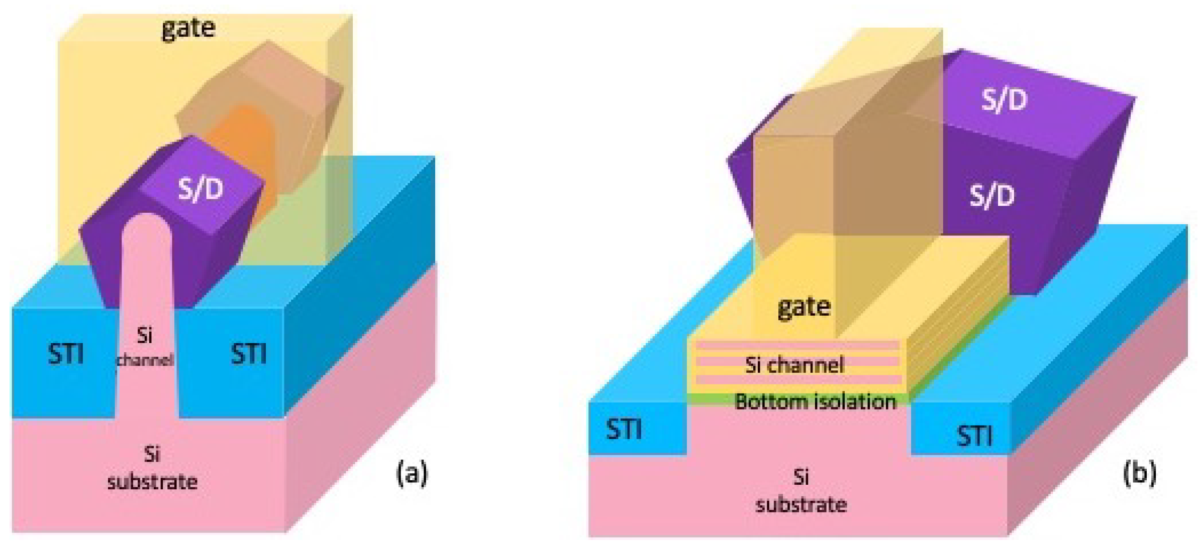
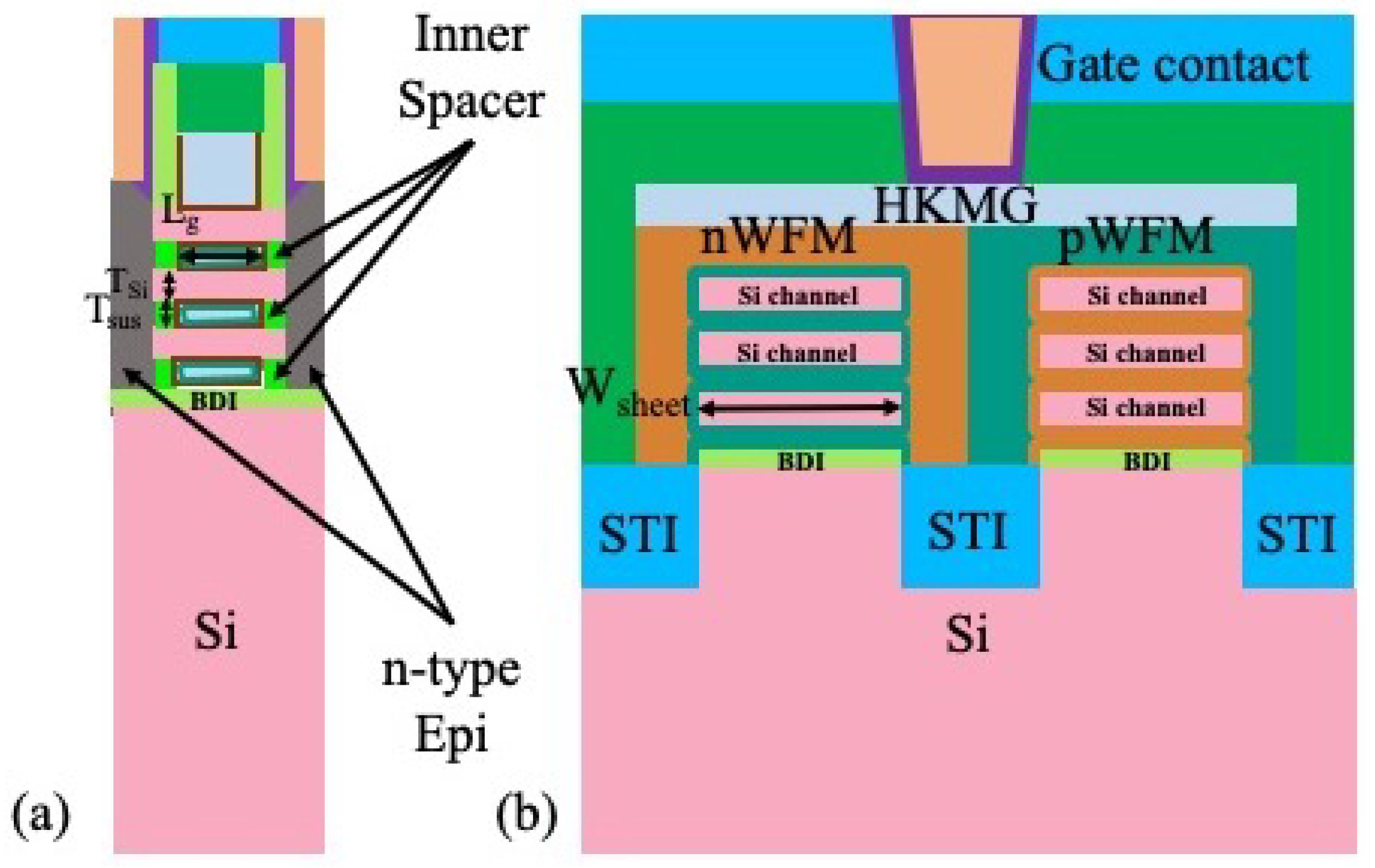
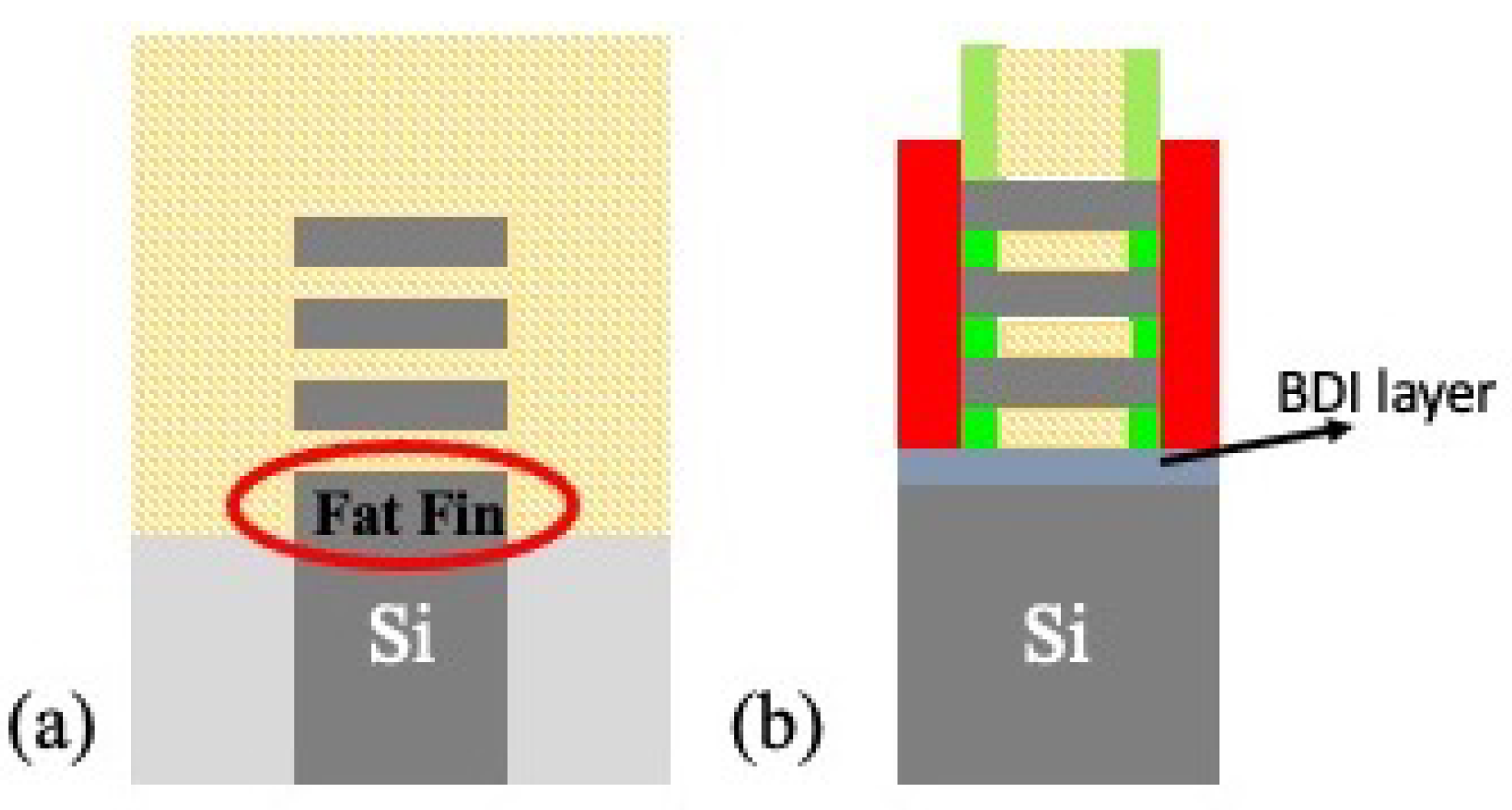
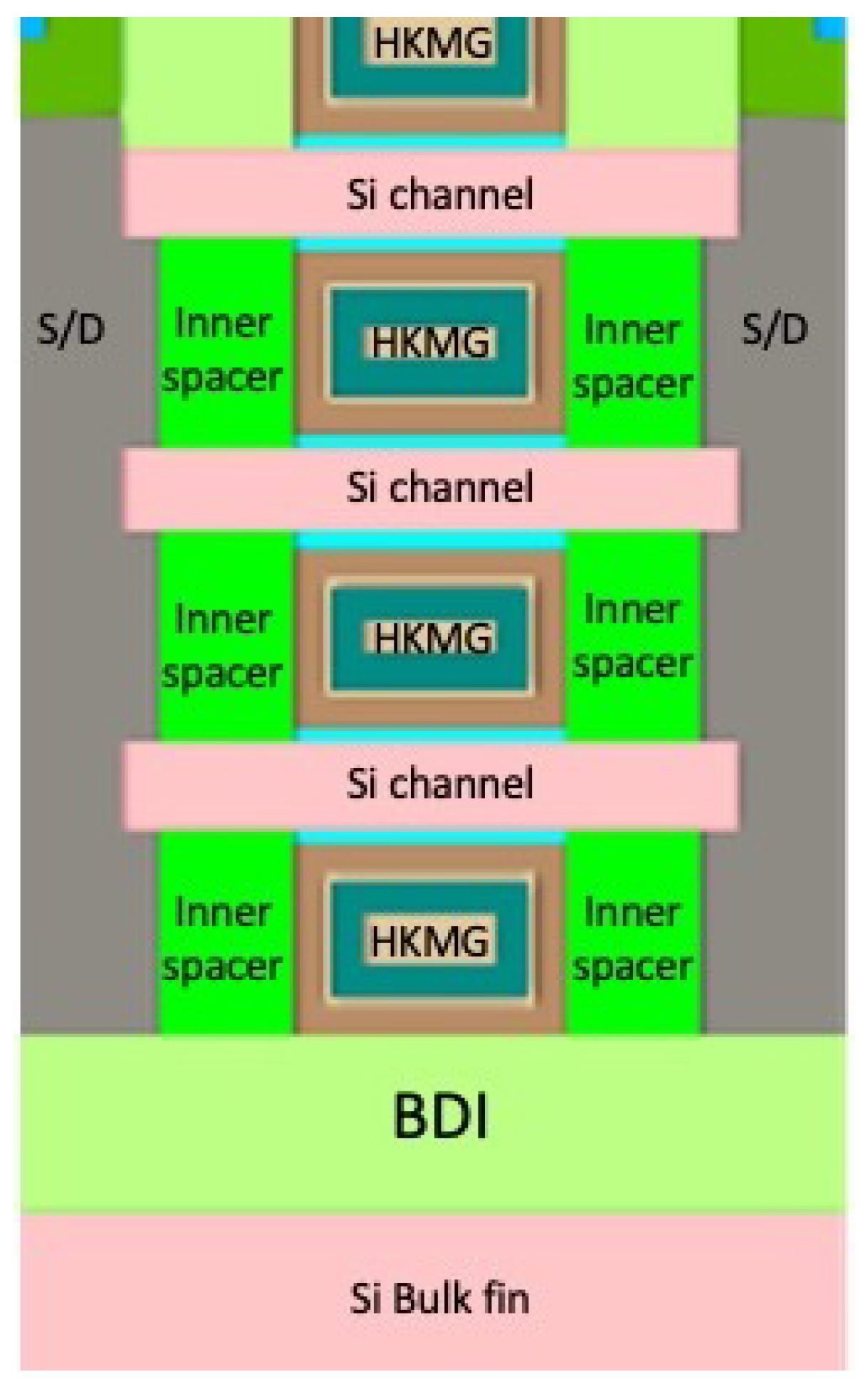
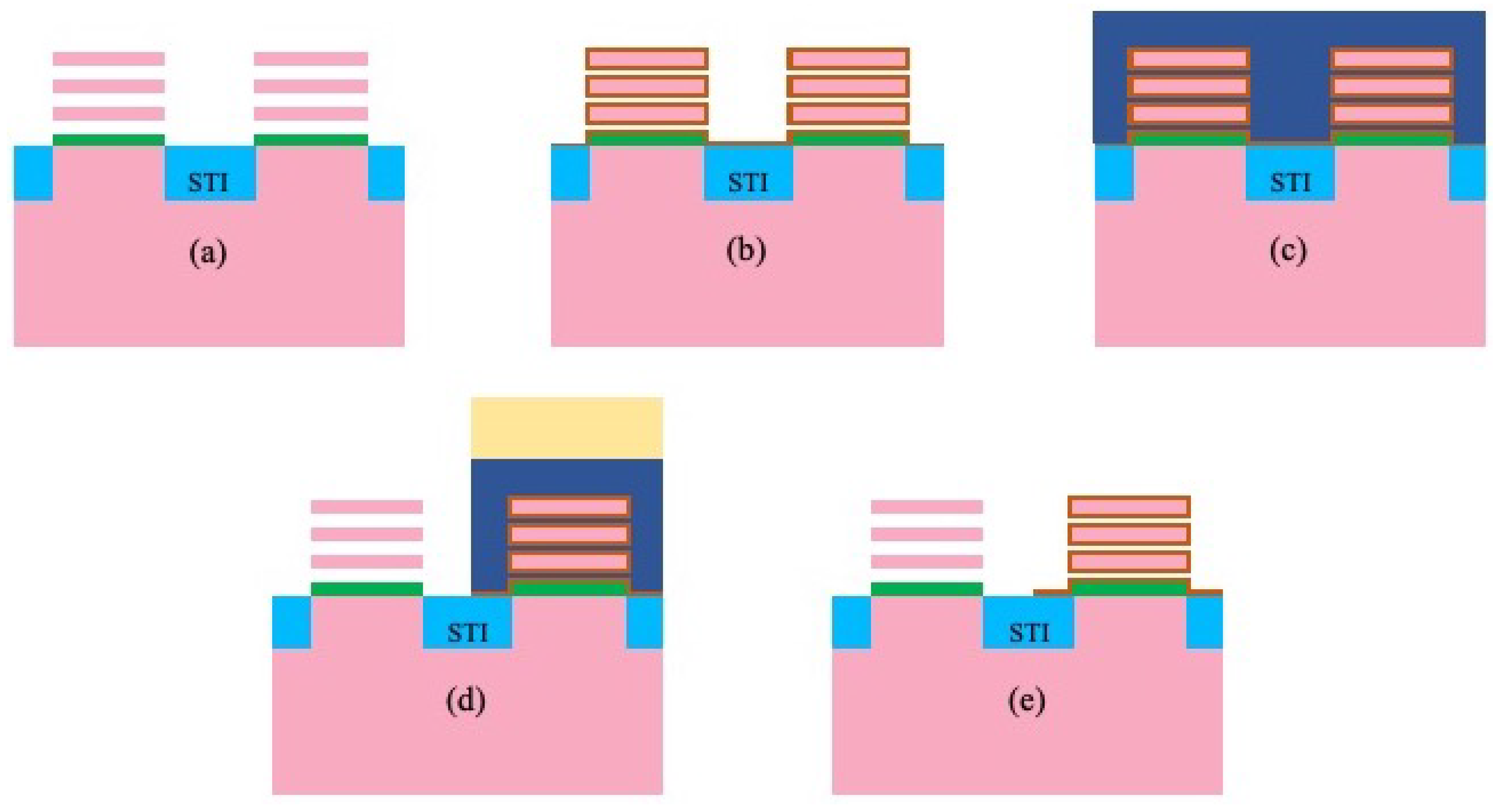
3. Full Bottom Dielectric Isolation
3.1. Integration
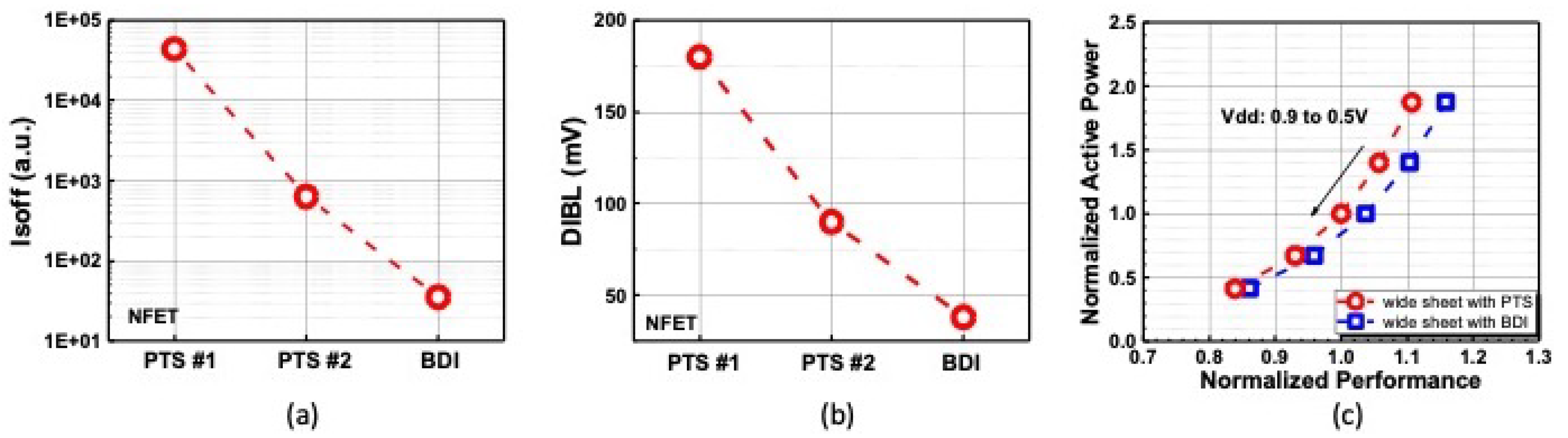
3.2. Experiments
3.3. Results and Discussion
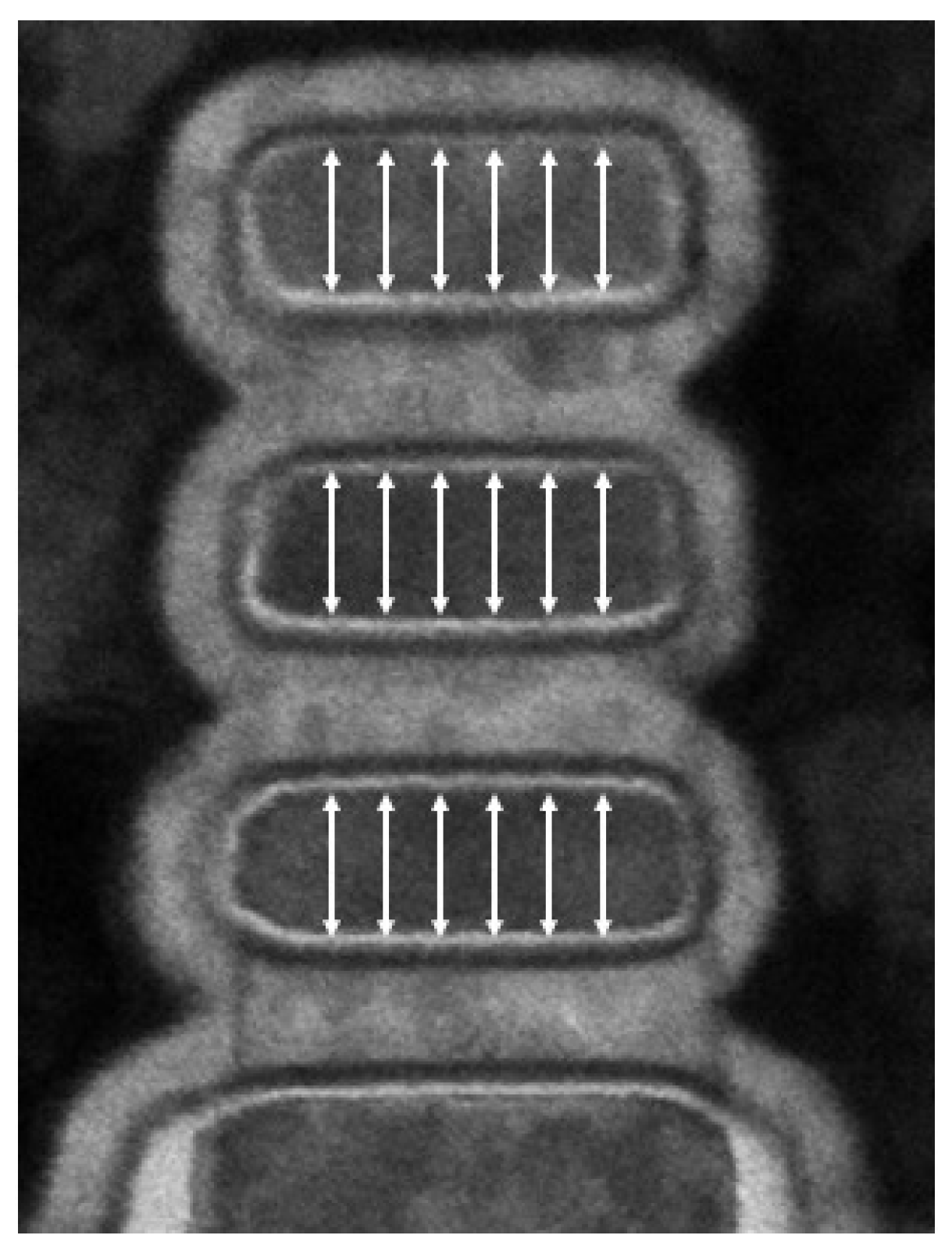
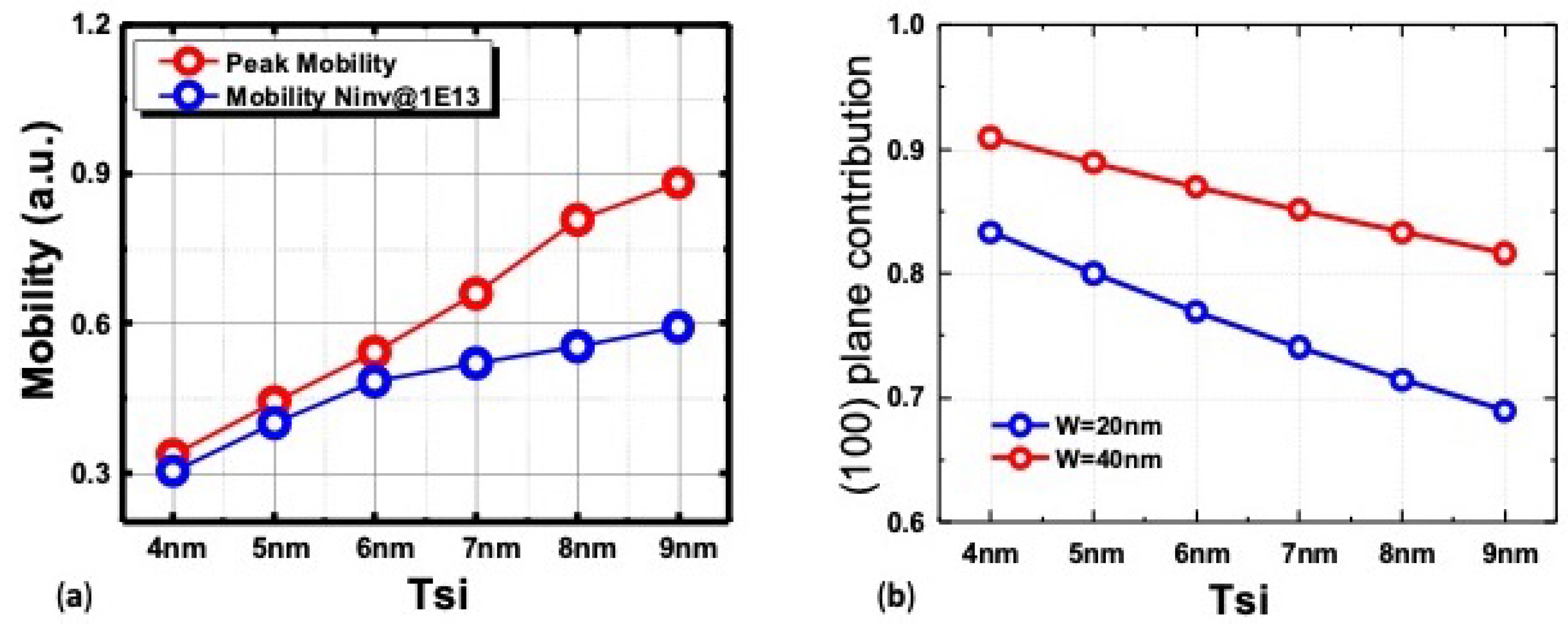
4. Channel Geometry Impact
4.1. Experiments
4.2. Results and Discussion
5. Enabling Multiple Threshold Voltages
5.1. Integration
Volumeless Multiple Threshold Voltages
5.2. Results and Discussions
6. Current Challenges
7. Future Outlook
8. On the Horizon
Author Contributions
Funding
Data Availability Statement
Acknowledgments
Conflicts of Interest
Abbreviations
| GAA FETs | Gate-All-Around Field Effect Transistors |
| BDI | Bottom Dielectric Isolation |
| STI | Shallow Trench Isolation |
| WFM | Work Function Metal |
| HKMG | High-k Metal Gate |
| SCE | Short Channel Effects |
| RMG | Replacement Metal Gate |
| PTS | Punch Through Stopper |
| MOL | Middle of Line |
| BEOL | Back End of Line |
| S/D | Source/Drain |
| DIBL | Drain Induced Barrier Lowering |
| TEM | Transmission Electron Microscopy |
| VTFET | Vertical Transport Field Effect Transistors |
| PPA | Power, Performance, and Area |
| BPR | Buried Power Rail |
| BSPDN | Back-Side Power Delivery Network |
| CPP | Contact Poly Pitch |
References
- The International Roadmap for Devices and Systems: 2021. Available online: https://irds.ieee.org/images/files/pdf/2021/2021IRDS_MM.pdf (accessed on 2 October 2022).
- Lee, S.-Y.; Kim, S.-M.; Yoon, E.-J.; Oh, C.-W.; Chung, I.; Park, D.; Kim, K. Three-dimensional MBCFET as an ultimate transistor. IEEE Electron Device Lett. 2004, 25, 217–219. [Google Scholar] [CrossRef]
- Bangsaruntip, S.; Cohen, G.M.; Majumdar, A.; Zhang, Y.; Engelmann, S.U.; Fuller, N.C.M.; Gignac, L.M.; Mittal, S.; Newbury, J.S.; Guillorn, M.; et al. High performance and highly uniform gate-all-around silicon nanowire MOSFETs with wire size dependent scaling. In Proceedings of the 2009 IEEE International Electron Devices Meeting (IEDM), Baltimore, MD, USA, 7–9 December 2009; pp. 1–4. [Google Scholar] [CrossRef]
- Kuhn, K.J. Considerations for Ultimate CMOS Scaling. IEEE Trans. Electron Devices 2012, 59, 1813–1828. [Google Scholar] [CrossRef]
- Lauer, I.; Loubet, N.; Kim, S.D.; Ott, J.A.; Mignot, S.; Venigalla, R.; Yamashita, T.; Standaert, T.; Faltermeier, J.; Basker, V.; et al. Si nanowire CMOS fabricated with minimal deviation from RMG FinFET technology showing record performance. In Proceedings of the 2015 Symposium on VLSI Technology (VLSI Technology), Kyoto, Japan, 16–18 June 2015; pp. 140–141. [Google Scholar]
- Mertens, H.; Ritzenthaler, R.; Hikavyy, A.; Kim, M.S.; Tao, Z.; Wostyn, K.; Chew, S.A.; De Keersgieter, A.; Mannaert, G.; Rosseel, E.; et al. Gate-all-around MOSFETs based on vertically stacked horizontal Si nanowires in a replacement metal gate process on bulk Si substrates. In Proceedings of the 2016 IEEE Symposium on VLSI Technology, Honolulu, HI, USA, 14–16 June 2016; pp. 1–2. [Google Scholar] [CrossRef]
- Mertens, H.; Ritzenthaler, R.; Chasin, A.; Schram, T.; Kunnen, E.; Hikavyy, A.; Ragnarsson, L.-Å.; Dekkers, H.; Hopf, T.; Wostyn, K.; et al. Vertically stacked gate-all-around Si nanowire CMOS transistors with dual work function metal gates. In Proceedings of the 2016 IEEE International Electron Devices Meeting (IEDM), San Francisco, CA, USA, 3–7 December 2016; pp. 19.7.1–19.7.4. [Google Scholar] [CrossRef]
- Loubet, N.; Hook, T.; Montanini, P.; Yeung, C.-W.; Kanakasabapathy, S.; Guillom, M.; Yamashita, T.; Zhang, J.; Miao, X.; Wang, J.; et al. Stacked nanosheet gate-all-around transistor to enable scaling beyond FinFET. In Proceedings of the 2017 Symposium on VLSI Technology, Kyoto, Japan, 5–8 June 2017; pp. T230–T231. [Google Scholar] [CrossRef]
- Veeraraghavan, S.; Fossum, J.G. Short-channel effects in SOI MOSFETs. IEEE Trans. Electron Devices 1989, 36, 522–528. [Google Scholar] [CrossRef]
- Ghani, T.; Armstrong, M.; Auth, C.; Bost, M.; Charvat, P.; Glass, G.; Hoffmann, T.; Johnson, K.; Kenyon, C.; Klaus, J.; et al. A 90nm high volume manufacturing logic technology featuring novel 45nm gate length strained silicon CMOS transistors. In Proceedings of the IEEE International Electron Devices Meeting 2003, Washington, DC, USA, 8–10 December 2003; pp. 11.6.1–11.6.3. [Google Scholar] [CrossRef]
- Mistry, K.; Allen, C.; Auth, C.; Beattie, B.; Bergstrom, D.; Bost, M.; Brazier, M.; Buehler, M.; Cappellani, A.; Chau, R.; et al. A 45nm Logic Technology with High-k+Metal Gate Transistors, Strained Silicon, 9 Cu Interconnect Layers, 193nm Dry Patterning, and 100% Pb-free Packaging. In Proceedings of the 2007 IEEE International Electron Devices Meeting, Washington, DC, USA, 10–12 December 2007; pp. 247–250. [Google Scholar] [CrossRef]
- Auth, C.; Allen, C.; Blattner, A.; Bergstrom, D.; Brazier, M.; Bost, M.; Buehler, M.; Chikarmane, V.; Ghani, T.; Glassman, T.; et al. A 22 nm high performance and low-power CMOS technology featuring fully-depleted tri-gate transistors, self-aligned contacts and high density MIM capacitors. In Proceedings of the 2012 Symposium on VLSI Technology (VLSIT), Honolulu, HI, USA, 12–14 June 2012; pp. 131–132. [Google Scholar] [CrossRef]
- Xie, R.; Montanini, P.; Akarvardar, K.; Tripathi, M.; Haran, B.; Johnson, S.; Hook, T.; Hamieh, B.; Corliss, D.; Wang, J.; et al. A 7 nm FinFET technology featuring EUV patterning and dual strained high mobility channels. In Proceedings of the 2016 IEEE International Electron Devices Meeting (IEDM), San Francisco, CA, USA, 3–7 December 2016; pp. 2.7.1–2.7.4. [Google Scholar] [CrossRef]
- Narendar, V.; Mishra, R.A. Analytical modeling and simulation of multigate FinFET devices and the impact of high-k dielectrics on short channel effects (SCEs). Superlattices Microstruct. 2015, 85, 357–369. [Google Scholar] [CrossRef]
- Kim, S.-D.; Guillorn, M.; Lauer, I.; Oldiges, P.; Hook, T.; Na, M.-H. Performance trade-offs in FinFET and gate-all-around device architectures for 7 nm-node and beyond. In Proceedings of the 2015 IEEE SOI-3D-Subthreshold Microelectronics Technology Unified Conference (S3S), Rohnert Park, CA, USA, 5–8 October 2015; pp. 1–3. [Google Scholar] [CrossRef]
- Bae, G.; Bae, B.-I.; Kang, M.; Hwang, S.M.; Kim, S.S.; Seo, B.; Kwon, T.Y.; Lee, T.J.; Moon, C.; Choi, Y.M.; et al. 3nm GAA Technology featuring Multi-Bridge-Channel FET for Low Power and High Performance Applications. In Proceedings of the 2018 IEEE International Electron Devices Meeting (IEDM), San Francisco, CA, USA, 1–5 December 2018; pp. 28.7.1–28.7.4. [Google Scholar] [CrossRef]
- Mochizuki, S.; Bhuiyan, M.; Zhou, H.; Zhang, J.; Stuckert, E.; Li, J.; Zhao, K.; Wang, M.; Basker, V.; Loubet, N.; et al. Stacked Gate-All-Around Nanosheet pFET with Highly Compressive Strained Si1-xGex Channel. In Proceedings of the 2020 IEEE International Electron Devices Meeting (IEDM), San Francisco, CA, USA, 12–18 December 2020; pp. 2.3.1–2.3.4. [Google Scholar] [CrossRef]
- Tsutsui, G.; Mochizuki, S.; Loubet, N.; Bedell, S.W.; Sadana, D.K. Strain engineering in functional materials. AIP Adv. 2019, 9, 030701. [Google Scholar] [CrossRef] [Green Version]
- Murray, C.E.; Yan, H.; Lavoie, C.; Jordan-Sweet, J.; Pattammattel, A.; Reuter, K.; Hasanuzzaman, M.; Lanzillo, N.; Robison, R.; Loubet, N. Mapping of the mechanical response in Si/SiGe nanosheet device geometries. Commun. Eng. 2022, 1, 11. [Google Scholar] [CrossRef]
- Zhang, J.; Ando, T.; Yeung, C.W.; Wang, M.; Kwon, O.; Galatage, R.; Chao, R.; Loubet, N.; Moon, B.K.; Bao, R.; et al. High-k metal gate fundamental learning and multi-Vt options for stacked nanosheet gate-all-around transistor. In Proceedings of the 2017 IEEE International Electron Devices Meeting (IEDM), San Francisco, CA, USA, 2–6 December 2017; pp. 22.1.1–22.1.4. [Google Scholar] [CrossRef]
- Bao, R.; Watanabe, K.; Zhang, J.; Guo, J.; Zhou, H.; Gaul, A.; Sankarapandian, M.; Li, J.; Hubbard, A.R.; Vega, R.; et al. Multiple-Vt Solutions in Nanosheet Technology for High Performance and Low Power Applications. In Proceedings of the 2019 IEEE International Electron Devices Meeting (IEDM), San Francisco, CA, USA, 7–11 December 2019; pp. 11.2.1–11.2.4. [Google Scholar] [CrossRef]
- Bao, R.; Durfee, C.; Zhang, J.; Qin, L.; Rozen, J.; Zhou, H.; Li, J.; Mukesh, S.; Pancharatnam, S.; Zhao, K.; et al. Critical Elements for Next Generation High Performance Computing Nanosheet Technology. In Proceedings of the 2021 IEEE International Electron Devices Meeting (IEDM), San Francisco, CA, USA, 13–15 December 2021; pp. 26.3.1–26.3.4. [Google Scholar] [CrossRef]
- Yeung, C.W.; Zhang, J.; Chao, R.; Kwon, O.; Vega, R.; Tsutsui, G.; Miao, X.; Zhang, C.; Sohn, C.-W.; Moon, B.K.; et al. Channel Geometry Impact and Narrow Sheet Effect of Stacked Nanosheet. In Proceedings of the 2018 IEEE International Electron Devices Meeting (IEDM), San Francisco, CA, USA, 1–5 December 2018; pp. 28.6.1–28.6.4. [Google Scholar] [CrossRef]
- Zhang, J.; Frougier, J.; Greene, A.; Miao, X.; Yu, L.; Vega, R.; Montanini, P.; Durfee, C.; Gaul, A.; Pancharatnam, S.; et al. Full Bottom Dielectric Isolation to Enable Stacked Nanosheet Transistor for Low Power and High Performance Applications. In Proceedings of the 2019 IEEE International Electron Devices Meeting (IEDM), San Francisco, CA, USA, 7–11 December 2019; pp. 11.6.1–11.6.4. [Google Scholar] [CrossRef]
- Loubet, N.; Kal, S.; Alix, C.; Pancharatnam, S.; Zhou, H.; Durfee, C.; Belyansky, M.; Haller, N.; Watanabe, K.; Devarajan, T.; et al. A Novel Dry Selective Etch of SiGe for the Enablement of High Performance Logic Stacked Gate-All-Around NanoSheet Devices. In Proceedings of the 2019 IEEE International Electron Devices Meeting (IEDM), San Francisco, CA, USA, 7–11 December 2019; pp. 11.4.1–11.4.4. [Google Scholar] [CrossRef]
- Bao, R.; Zhou, H.; Wang, M.; Guo, D.; Haran, B.S.; Narayanan, V.; Divakaruni, R. Extendable and Manufacturable Volume-less Multi-Vt Solution for 7 nm Technology Node and Beyond. In Proceedings of the 2018 IEEE International Electron Devices Meeting (IEDM), San Francisco, CA, USA, 1–5 December 2018; pp. 28.5.1–28.5.4. [Google Scholar] [CrossRef]
- Bao, R.; Greene, B.; Kwon, U.; Lee, S.; Bruley, J.; Wang, W.; Zhao, K.; DeHaven, P.W.; Li, Z.; Wong, K.; et al. Replacement metal gate resistance in FinFET architecture modelling, validation and extendibility. In Proceedings of the 2015 IEEE International Electron Devices Meeting (IEDM), Washington, DC, USA, 7–9 December 2015; pp. 34.3.1–34.3.4. [Google Scholar] [CrossRef]
- Cai, L.; Chen, W.; Du, G.; Kang, J.; Zhang, X.; Liu, X. Investigation of self-heating effect on stacked nanosheet GAA transistors. In Proceedings of the 2018 International Symposium on VLSI Technology, Systems and Application (VLSI-TSA), Hsinchu, Taiwan, 16–19 April 2018; pp. 1–2. [Google Scholar] [CrossRef]
- Bury, E.; Kaczer, B.; Linten, D.; Witters, L.; Mertens, H.; Waldron, N.; Zhou, X.; Collaert, N.; Horiguchi, N.; Spessot, A.; et al. Self-heating in FinFET and GAA-NW using Si, Ge and III/V channels. In Proceedings of the 2016 IEEE International Electron Devices Meeting (IEDM), San Francisco, CA, USA, 3–7 December 2016; pp. 15.6.1–15.6.4. [Google Scholar]
- Rathore, S.; Jaisawal, R.K.; Kondekar, P.N.; Bagga, N. Design Optimization of Three-Stacked Nanosheet FET From Self-Heating Effects Perspective. IEEE Trans. Device Mater. Reliab. 2022, 22, 396–402. [Google Scholar] [CrossRef]
- Lee, K.-S.; Park, J.-Y. Inner Spacer Engineering to Improve Mechanical Stability in Channel-Release Process of Nanosheet FETs. Electronics 2021, 10, 1395. [Google Scholar] [CrossRef]
- Yang, X.; Li, X.; Liu, Z.; Sun, Y.; Liu, Y.; Li, X.; Shi, Y. Impact of Process Variation on Nanosheet Gate-All-Around Complementary FET (CFET). IEEE Trans. Electron Devices 2022, 69, 4029–4036. [Google Scholar] [CrossRef]
- Xia, G.; Hoyt, J.L.; Canonico, M. Si–Ge Interdiffusion in Strained Si/Strained SiGe Heterostructures and Implications for Enhanced Mobility Metal-Oxide-Semiconductor Field-Effect Transistors. J. Appl. Phys. 2007, 101, 044901. [Google Scholar] [CrossRef]
- Dong, Y. A Systematic Study of Silicon Germanium Interdiffusion for Next Generation Semiconductor Devices (T); University of British Columbia: Vancouver, BC, Canada, 2014; Available online: https://open.library.ubc.ca/collections/ubctheses/24/items/1.0167516 (accessed on 2 October 2022).
- Thornton, C.; Tuttle, B.; Turner, E.; Law, M.; Pantelides, S.; Wang, G.; Jones, K. The Diffusion Mechanism of Ge During Oxidation of Si/SiGe Nanofins. ACS Appl. Mater. Interfaces 2022, 14, 29422–29430. [Google Scholar] [CrossRef]
- Prasad, D.; Teja Nibhanupudi, S.S.; Das, S.; Zografos, O.; Chehab, B.; Sarkar, S.; Baert, R.; Robinson, A.; Gupta, A.; Spessot, A.; et al. Buried Power Rails and Back-side Power Grids: Arm® CPU Power Delivery Network Design Beyond 5 nm. In Proceedings of the 2019 IEEE International Electron Devices Meeting (IEDM), San Francisco, CA, USA, 7–11 December 2019; pp. 19.1.1–19.1.4. [Google Scholar] [CrossRef]
- Salahuddin, S.; Perumkunnil, M.; Dentoni Litta, E.; Gupta, A.; Weckx, P.; Ryckaert, J.; Na, M.H.; Spessot, A. Buried Power SRAM DTCO and System-Level Benchmarking in N3. In Proceedings of the 2020 IEEE Symposium on VLSI Technology, Honolulu, HI, USA, 16–19 June 2020; pp. 1–2. [Google Scholar] [CrossRef]
- Chen, R.; Sisto, G.; Jourdain, A.; Hiblot, G.; Stucchi, M.; Kakarla, N.; Chehab, B.; Salahuddin, S.M.; Schleicher, F.; Veloso, A.; et al. Design and Optimization of SRAM Macro and Logic Using Backside Interconnects at 2 nm node. In Proceedings of the 2021 IEEE International Electron Devices Meeting (IEDM), San Francisco, CA, USA, 13–15 December 2021; pp. 22.4.1–22.4.4. [Google Scholar] [CrossRef]
- Jagannathan, H.; Anderson, B.; Sohn, C.-W.; Tsutsui, G.; Strane, J.; Xie, R.; Fan, S.; Kim, K.-I.; Song, S.; Sieg, S.; et al. Vertical-Transport Nanosheet Technology for CMOS Scaling beyond Lateral-Transport Devices. In Proceedings of the 2021 IEEE International Electron Devices Meeting (IEDM), San Francisco, CA, USA, 13–15 December 2021; pp. 26.1.1–26.1.4. [Google Scholar] [CrossRef]
- Wang, J.; Suk, S.D.; Chu, A.; Hook, T.; Young, A.; Krishnan, R.; Bao, R.; Seshadri, I.; Senapati, B.; Zalani, V.; et al. Challenges and Opportunities for Stacked Transistor: DTCO and Device. In Proceedings of the 2021 Symposium on VLSI Technology, Kyoto, Japan, 13–19 June 2021; pp. 1–2. [Google Scholar]
- Das, S.; Sebastian, A.; Pop, E.; McClellan, C.J.; Franklin, A.D.; Grasser, T.; Knobloch, T.; Illarionov, Y.; Penumatcha, A.V.; Appenzeller, J.; et al. Transistors based on two-dimensional materials for future integrated circuits. Nat. Electron. 2021, 4, 786–799. [Google Scholar] [CrossRef]
- Rai, A.; Movva, H.C.P.; Roy, A.; Taneja, D.; Chowdhury, S.; Banerjee, S.K. Progress in Contact, Doping and Mobility Engineering of MoS2: An Atomically Thin 2D Semiconductor. Crystals 2018, 8, 316. [Google Scholar] [CrossRef] [Green Version]
- Akinwande, D.; Huyghebaert, C.; Wang,, C.-H.; Serna, M.I.; Goossens, S.; Li, L.-J.; Wong, H.-S.P.; Koppens, F.H.L. Graphene and two-dimensional materials for silicon technology. Nature 2019, 573, 507–518. [Google Scholar] [CrossRef]
- Bierwagen, O. Indium oxide—A transparent, wide-band gap semiconductor for (opto)electronic applications. Semicond. Sci. Technol. 2015, 30, 024001. [Google Scholar] [CrossRef]


Publisher’s Note: MDPI stays neutral with regard to jurisdictional claims in published maps and institutional affiliations. |
© 2022 by the authors. Licensee MDPI, Basel, Switzerland. This article is an open access article distributed under the terms and conditions of the Creative Commons Attribution (CC BY) license (https://creativecommons.org/licenses/by/4.0/).
Share and Cite
Mukesh, S.; Zhang, J. A Review of the Gate-All-Around Nanosheet FET Process Opportunities. Electronics 2022, 11, 3589. https://doi.org/10.3390/electronics11213589
Mukesh S, Zhang J. A Review of the Gate-All-Around Nanosheet FET Process Opportunities. Electronics. 2022; 11(21):3589. https://doi.org/10.3390/electronics11213589
Chicago/Turabian StyleMukesh, Sagarika, and Jingyun Zhang. 2022. "A Review of the Gate-All-Around Nanosheet FET Process Opportunities" Electronics 11, no. 21: 3589. https://doi.org/10.3390/electronics11213589