1. Introduction
With recent technological advancements, the internet of things (IoT) is nowadays at the cutting edge of transforming various fields to a level of smartness by storing and processing data in a distributed manner to enhance productivity.
Internet of things (IoT) technology is based on powerful wireless devices interconnected in a complex ecosystem that enables one to gather, share, and analyze information and take actions appropriately [
1]. These wireless devices are called sensor nodes, dispersed through different technologies and communicating at different frequency levels in a wide network.A number of applications such as weather [
2], health, military, transport, localization [
3,
4], and smart automotive depend on the potential of sensor nodes to overcome the challenges of wireless sensor nodes [
5]. In contrast, the specific requirements and performances for sensor nodes obviously depend on the application they will serve [
6], the effect to be sensed, the amount of the data rate transferred [
7], and subsequently on the power consumed [
8]. Data rate, transmission power, and power consumption in the sensor node are also related to the operating frequency.
Some RF bands, such as
and 5 GHz, are highly populated bands that enable connectivity and coverage but face much interference from the extensive demand of other devices. Additionally, those RF bands suffer from path losses, low communication range, and require multi-hop communications, which results in the need for a large number of devices connected to the network [
9]. The results of this are increasing complexity and synchronization issues. On the other hand, operating in sub-gigahertz band frequencies, e.g., the 868 MHz band, seems to be a promising solution for the improvement of coverage and connectivity [
10]. Additionally, it enhances the communication range in indoor applications with many obstacles and distributing factors. Furthermore, improving the receiver node’s sensitivity could also enhance the communication range alongside the operating frequency.
Wireless communication is defined as “over the air” to create a telecommunications channel between two points. Technologies differ from the used frequency channel and the operating techniques used for successful radio transmission. In recent works, many technologies have been introduced such as infrared communication, satellite communication, microwave transmission, wireless fidelity (Wi-Fi), worldwide interoperability for microwave access (WiMAX), long term evolution (LTE), the field area network (FAN), etc. [
11]. Aiming for reliable and power-efficient wireless communication is the common concern of all used technologies, and that is the reason behind implementing smart techniques for improving network specifications. An example is code division multiple access (CDMA), which is a channel multiple access technique, where several transmitters can send information simultaneously over a single communication channel [
12]. This approach improves the quality of service and real-time communication schemes which reduce the consumed energy and guarantee better link qualifications. Recent research using the efficient uplink protocol works within the range of mW-W of power consumption, which is much higher than the required power consumption for the proposed sensor nodes. Investigating hardware-based techniques which implement a pure asynchronous rendezvous can decrease the power hunger of the normal receivers compared with other technologies.
The implementation of the wake-up receiver (WuRx) nodes is an essential investigation in the WSN. The WuRx approach represents a promising solution with which to implement an energy-efficient network operation with low latency [
6]. Alongside always-on transceivers, power gates with an appropriate duty cycle are also investigated. Among the challenges of wireless sensor nodes, the communication range is not the only essential matter for improving internet of things (IoT) applications; the minimization of the power consumption of sensor nodes is nowadays also a concern of researchers and developers in this field [
13]. Furthermore, maximizing the battery life-time is a crucial parameter for energy-efficient applications [
14].
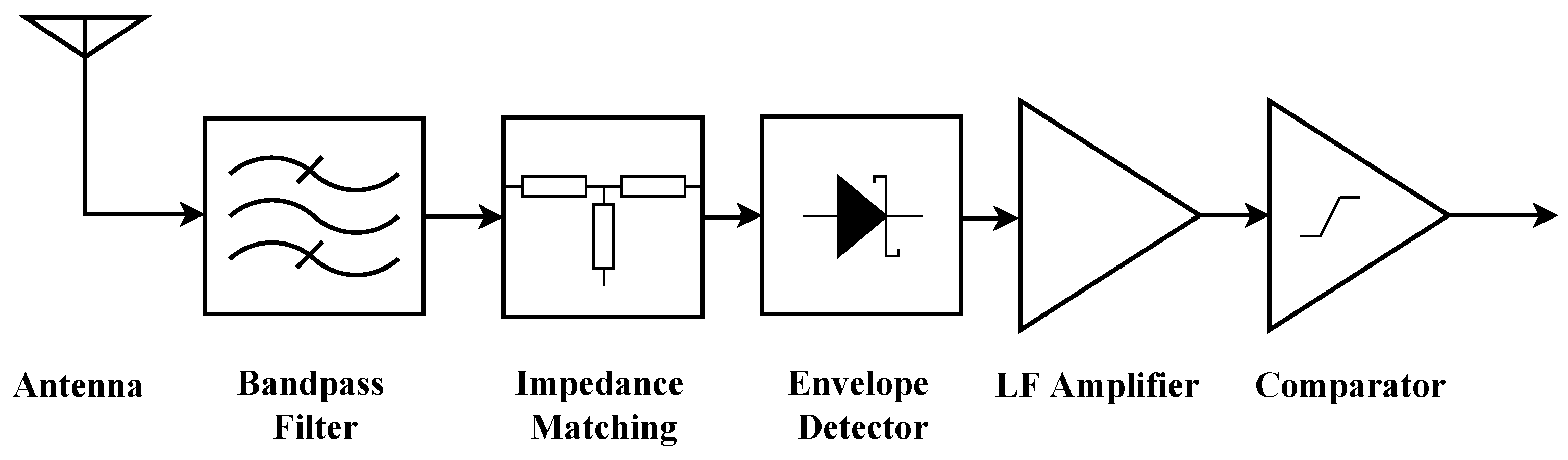
The standard building block of a wake-up receiver circuit is based on passive components and called the direct RF architecture as presented in
Figure 1. It is an always-on circuit which has the role of identifying the wake-up packet (WuPt). Once the identifier of the WuRx recognizes that the received telegram corresponds to a WuPt, an interruption is generated and sent to the main radio, which changes the state immediately from sleep to active.
WuRx nodes are characterized by ultra-low battery-powered nodes, typically consume below 10 μW [
16] and ensure low latency. However, their sensitivity is related to the adopted architecture and whether it includes an LNA in the receiver front end or not. As with many other standard receivers, the integration of an LNA block in the front-end antenna has the role to boost the incoming RF signals and detect the lower ones.
In WuRx nodes based on direct RF architectures, many issues related to communication range and coverage appear while deploying a wireless network. This sensitivity limitation affects the performance of the whole network, while with the development of tuned RF (TRF) architecture with the integration of LNA in the receiver front-end, the limitation of sensitivity related to the envelope detector was improved.
Although many works with different technologies are available for the design of LNA, the requirements of LNA for a duty-cycled WuRx should be adhered to so as to maintain the overall circuit performances. The exigencies for designing an LNA for duty-cycled WuRx are primarily an ultra-low power consumption with good sensitivity and latency as well as settling time.
This work illustrates in detail the theoretical background for the design of the LNA with various trade-off performances. Additionally, the design is well structured from the simulation issues and hardware implementation points of view. The last part is dedicated to comparing the results of the designed LNA with those of a commercial off-the-shelf (COTS) LNA. MAX2640 is selected to be integrated into the same duty cycled WuRx board for accurate comparison and specific power consumption calculation. A discussion is also undertaken to evaluate the achieved results.
2. Low Noise Amplifier in Radio Frequency Front-End Antenna
Radio frequency (RF) amplifiers are indispensable to any wireless system. The RF amplifiers act as power amplifiers in transmitters or LNAs in the receivers. This paper focuses on the main functionality of the LNA, which is placed on the receiver side. In addition, several performances such as ultra-low power consumption and good sensitivity behavior should be considered in the designed LNA in the interest of implementing a WuRx node circuit operating at 868 MHz frequency [
15].
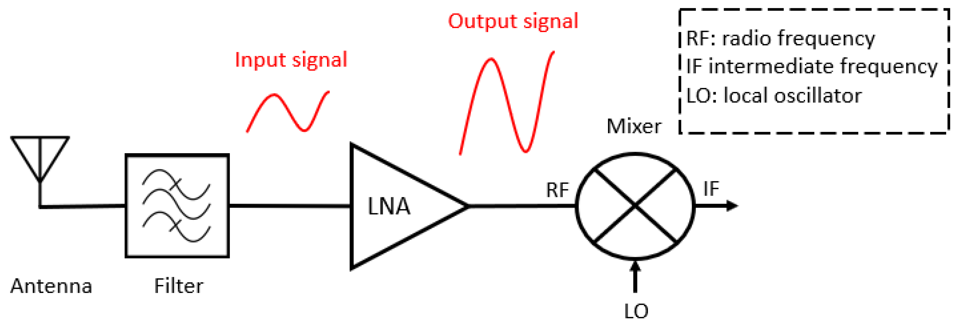
As wireless communication faces excessive noise, which is largely produced through the crosswalk of an electromagnetic wave in the air, the LNA could overcome this problem by amplifying the very low-power signal with minimal additive distortion at the receiver input. However, the noise present at the input of the amplifier could also introduce some amplification. Within the design, additional noise should be treated and minimized. In the front-end, the LNA is placed after a bandpass filter to improve the selectivity of the reception and to suppress the parasitic signals outside the 868 MHz.
Figure 2 shows the placement of LNA in the front-end antenna.
The amplitude of the weak signal entering the LNA is increased and prepared to be treated by the rest of the blocks. The treated signal is later introduced into the down-conversion mixer, where the signal’s frequency will be reduced. Thus, the rest of the blocks of the receiver operate at a lower frequency than the frequency of the LNA and mixer. It is essential to have an LNA with high performance in order to ensure the reliability of data transmission.
The main challenge of an LNA design is to make a trade-off between the following performances:
In the literature, LNA is used in many different fields [
17] including medical, transport, military, etc. The main purpose in various applications is always to increase gain in the receiver path with a minimum signal-to-noise ratio (SNR). The selection of transistors as well as the number of cascaded stages determine the type of LNA design.
2.1. Design and Implementation of Low Noise Amplifier from State of the Art Overview
In advanced wireless communication research, the increasing demand for receiver sensitivity has produced an exciting amount of work on LNA designs. The current architectures operate in different communication frequency ranges and utilize different topologies based on a bipolar junction transistor (BJT) or field-effect transistor (FET). Regarding design challenges, the LNAs presented in the state of the art (SoA) or in the commercialized prototypes tend to balance performances and provide a clear trade-off. For most internet of things (IoT) application scenarios based on WuRx, a sensitivity level of better than −70 dBm is required. However, in the state of the art, many WuRx works, including LNAs, either focus on high sensitivity with huge energy consumption or emphasize ultra-low power consumption together with low sensitivity.
An in-depth study of different LNA designs was conducted to meet the desired requirements.
Table 1 presents some LNA designs which are selected based on their architectural performances. Most of the selected LNA designs are based on metal-oxide semiconductor (CMOS) technology, representing the first selection criterion that did not match the required performances. This work will be developed based on discrete components due to its low-cost implementation, also for the reason that designing an RF circuit may lead to plenty of frequency problems such as shift and drift in magnificent proportions. Thus, using off-the-shelf components provides more flexibility in manufacturing and enhances moment-to-moment revision and changes in the architecture. The frequency shift problem could be solved by hardware tuning using lab equipment.
Taking as an example the design presented in [
21], which is based on off-the-shelf components, the 868 MHz band was included within the operational frequency range; however, the total current consumption of the circuit is extremely high and failed to achieve the need for low power consumption for the WuRx.
Most of the LNA works in SoA are made for mobile and radar communication applications operating in wide and ultra-wide bands. Conversely, the proposed LNA is designed for operating in 868 MHz. Thus, it is another factor that enhances the uniqueness of this work.
The in-depth study of LNA designs provided in the SoA is essential to strengthen the theoretical background behind RF design, and also to discover different architectures, and extract weaknesses and strengths behind the use of transistors with the best operating points and the RF signal behavior through the adopted design. The design specifications for the WuRx application are detailed in the following section.
2.2. Aimed Design Specifications and Requirements
Many commercialized LNAss were selected to compare their performances with the desired ones and to investigate how far they can adhere to the need for a developed WuRx.
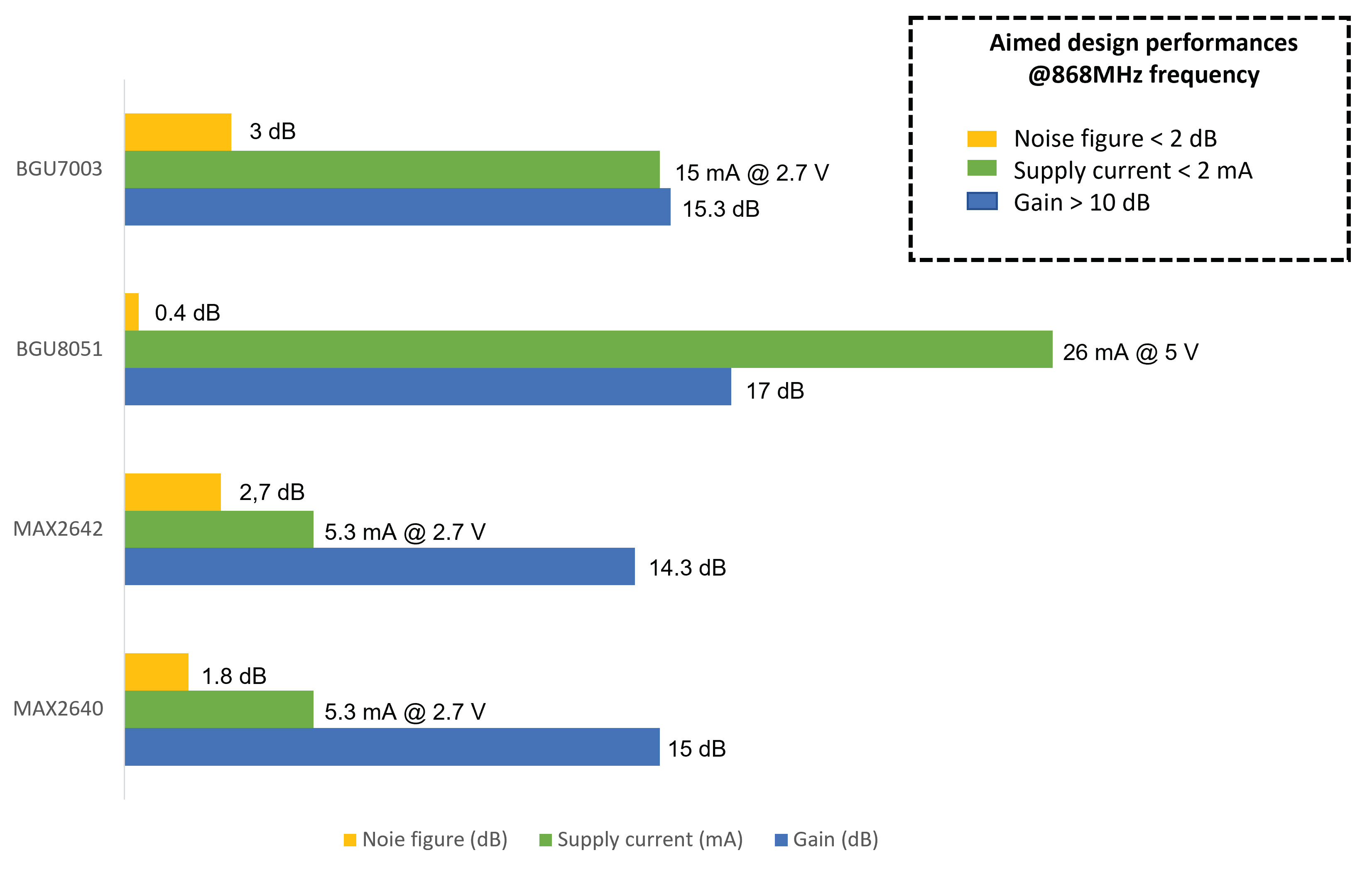
Table 2 summarizes the selection of different LNA designs for various applications. The table illustrates some mounted evaluation boards of LNA operation in 868 MHz. The comparison among different commercially available products mentions the technology used as well as performance parameters.
The trade-off between power consumption and gain is always a difficult task that can compromise the intended objectives. For example, BGU7003 and BGU8051X both reach a gain of 20 dB but consume, respectively, 15 mA and 36 mA, which can not be implemented in a circuit consuming some micro-watts in total.
The integration of LNA into WuRx should maintain the approach for ultra-low power consumption to conserve the overall system assumption [
28]. Compared to SoA, all LNAs operating at 868 MHz are power hungry. Therefore, the designed amplifier should consider the current currying in a single amplification stage in the range of 1–2 mA, with a flexibility increase if the need for higher gain becomes apparent in the adopted application.
Considering the stable range for the transistor operating characteristics, non-elevation of the voltage supply for feeding the active device is also a significant factor in keeping low current consumption. On the other hand, the excessive noise in wireless communication, which is largely produced at the receiver front end of RF receivers, is an inherent problem.
To overcome this problem, it is necessary to design the LNA by considering the concept of amplifying the incoming weak signals without adding further noise stages and minimizing them. The noise figure in the designed RF amplifier should not exceed 2 dB for one stage.
One of the most critical design requirements is to treat the system’s stability to ensure normal amplification behavior and avoid oscillating circuits. Stability is related to the determination of th s-parameters of the circuit, which also have the role of identifying the input and output return losses. Both factors should be kept below −10 dB to minimize reflections and ensure a maximum power transfer through the RF path.
Lastly, we mention the most critical design specification, which is the gain that situates the designed LNA well within the SoA by increasing the sensitivity of the receiver node. The mentioned design performances will be explained theoretically in the next section with the presentation of simulated results for each obtained parameter.
Achieving the simultaneous requirements of high gain, low current consumption, and a low noise figure are challenging tasks for balancing the trade-offs of the overall design. However, by analyzing
Figure 3, it is clear that the specifications set for the present work are very well considered in terms of current market trends.
The main focus of this work is to provide a solid structured design for the development and optimization of LNA for a given set of performance parameters.
3. Low Noise Amplifier Design Considerations and Simulation Results
In wireless communication systems, the LNA improves the receiver channel communication by boosting the received signal with the lowest possible noise figure (NF) addition. For an ideal LNA performance, all the design requirements should agree based on figures of merits such as stability, low noise figure, good gain, and excellent matching performance. All those performances were well studied and simulated to extract the best selection criteria for a stable LNA design.
3.1. Transistor Selection
A step that precedes the setting of the RF parameters is transistor selection which is the critical factor of the LNA design as long as the gain adopted in the LNA’s complete circuit derives essentially from the transistor’s internal gain. Additionally, the simultaneous requirements of the transistors are considered to be essential parameters for building the whole design. LNAs are constructed differently in the literature, either based on a bipolar junction transistor (BJT) or field-effect transistor (FET).
The meeting of requirements is also structured differently in both types. Field-effect transistors (FETs) feature better linearity and noise at a very high transition frequency [
29]. Furthermore, they require proper circuit stabilization, as they are prone to oscillate due to their high switching capabilities. However, BJTs lead to a better speed at the same physical attitude and price, as they have very little input capacitance. They can also provide better gain performance. BJTs can support higher output currents for signal outputs and have a lower output impedance. This is a considerable advantage for amplifiers built to drive a low input impedance load or deliver significant amounts of power [
30].
To conclude, the chosen transistor technology is the bipolar junction transistor (BJT) to achieve a low-cost LNA with a minimum number of external matching and biasing networks as standard requirements. Furthermore, it provides a certain degree of flexibility in order to alternate all the parameters. In this work, different families of bipolar junction transistors (BJTs) were tested under specific conditions to extract their response to design requirements. Finally, BFP740 was selected due to its good compromise between high gain and a low noise figure together with the lowest possible power consumption.
3.2. Architecture of LNA
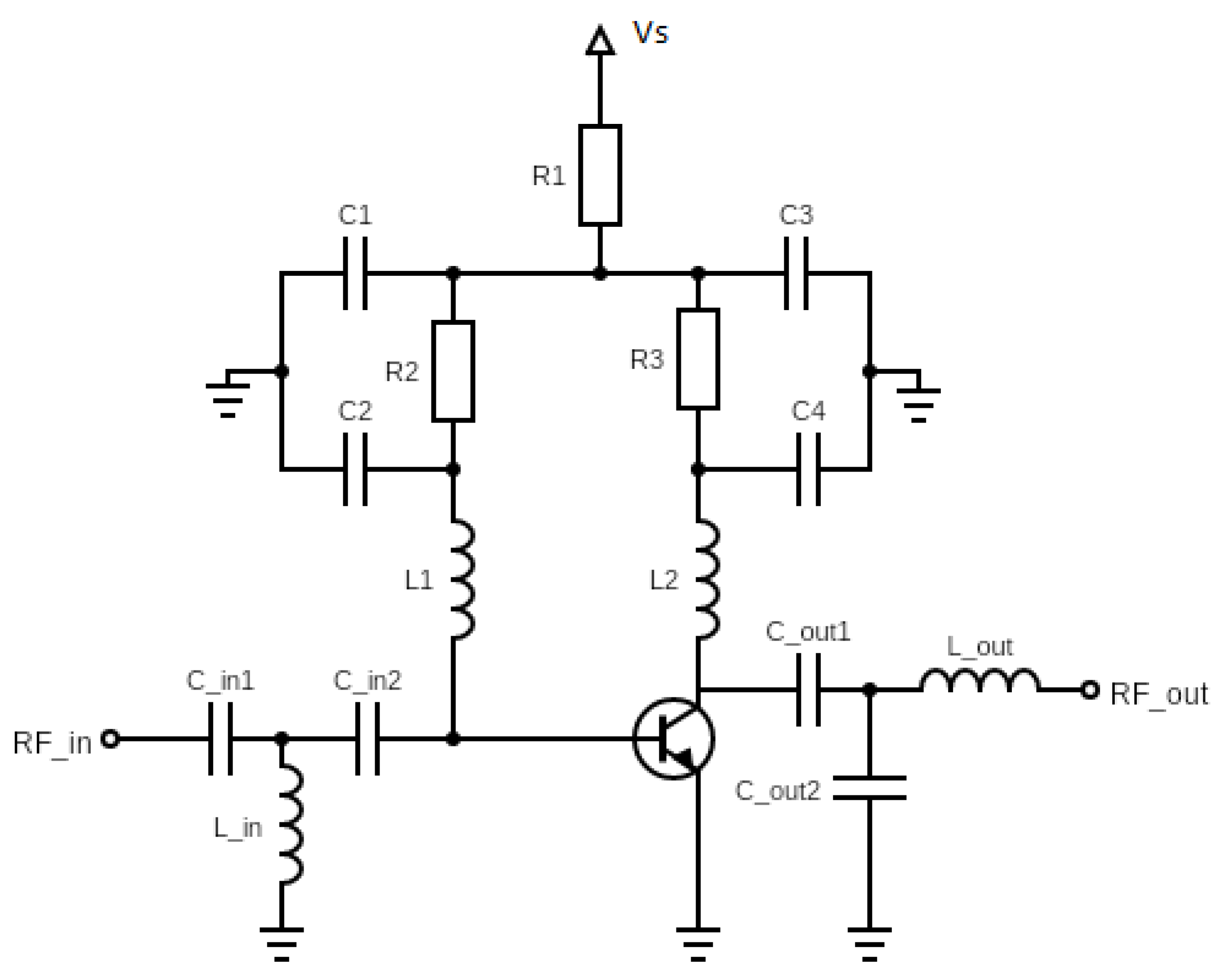
As described in
Section 3.1, the choice for the proposed application is BJTs due to their high performance. To enhance good amplification of the incoming signal, the BFP740 transistors are mounted in a common emitter (CE) architecture and operated by using an alternating current (AC) as the input signal. Compared to the common base (CB) topology, the CE topology delivers good gain and noise performance in a narrow bandwidth. For this topology, the amplifier input is taken from the base terminal, the output is collected from the collector terminal, and the emitter terminal is common for both terminals [
29].
Figure 4 shows the connection of the BFP740 in the proposed CE architecture, with the presence of a matching circuit to 50 Ohm in the input and output, respectively, using (C_in1, L_in2, C_in2 for input and C_out1, C_out2 and L_out for output). The inductors L1 and L2 handle the overpass of the RF signal through the micro strip-line from input to output. The resistance R2 is the biasing resistor, which is involved in determining the operating point. The resistors in the collector branch also serve to determine current consumption and introduce stability and linearity. The parallel capacitors decrease noise and also introduce the stability of the circuit.
During the simulation of the following design using the Advanced Design System (ADS), an important outcome is demonstrated: every component in the circuit does not have a single role. Working at a high-frequency level causes a very sensitive behavior for the component. Each element could introduce the role of others, and stability or matching could be degraded with every change in the simulation.
In conclusion, the tuning of certain values was performed carefully, considering after every iteration all the required performance of the LNA. Additionally, the trade-off between all desired performances is well studied to obtain the best results.
The studied architecture is implemented in ADS to determine the exact component values for an appropriate amplified signal behavior before implementation. ADS is a powerful simulation tool introduced in the pre and post-hardware phase. Before the hardware implementation, structuring the architecture, configuring the exact lumped component values, and extracting the best simulation results is the aim of running several simulations. After mounting the chosen component onto the printed board, ADS was used again to correct several hardware problems faced during the implementation phase.
This simulator has various advanced capabilities in high-frequency simulations and electromagnetic behavior recognition. As the first viewpoint for CE topology, the selected BFP740 transistor was integrated into the ADS library and supplied under different voltage levels to determine the chosen transistor’s operating conditions.
The Q-point is set at the lowest bias for a low-power design while providing the required gain. The design architecture is tuned with a DC power of 1–3 V, the gain was varied at 8–20 dB. Additionally, the current consumption changes with the tuning of voltage. The S-parameter resumes the input–output reflection factors, stability, noise figure, and gain resulting from . Furthermore, the linearity and the amplified transient signal are simulated and illustrated in the following sections.
3.3. Scattering Parameters Characterization and Simulation
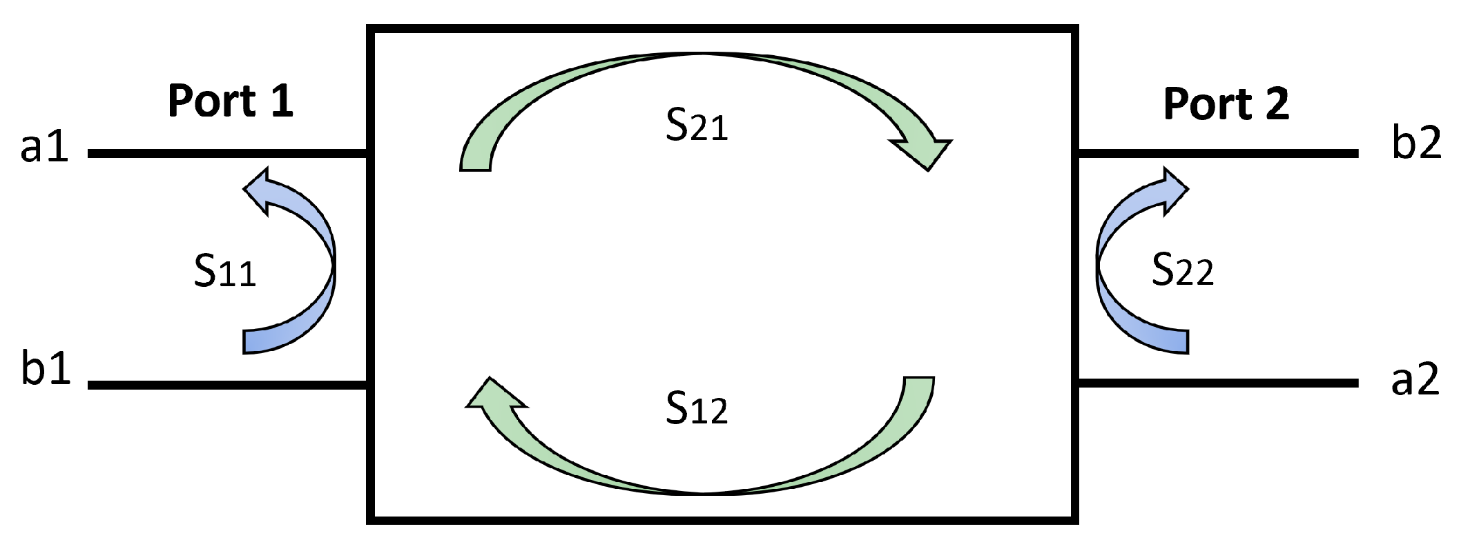
Since it is challenging to measure voltage or current in RF applications, the terms used to characterize the system performance and behavior are energy and power. The scattering parameters of the two-port system are the power characterization parameters. The S-parameters describe the relationship between the input and output of two ports of the system. A port is defined as input or output where voltage and current are delivered to ensure communication between two radios.
Considering the required LNA design as the RF system present in
Figure 5, port 1 is the input impedance, and port 2 is the output impedance of the system. The scattering parameters are as follows:
is the input reflection coefficient;
is the output reflection coefficient;
is the forward transmission coefficient;
is the reverse transmission coefficient.
Figure 5.
Identification of S-parameters in two-port system.
Figure 5.
Identification of S-parameters in two-port system.
A small-signal AC simulation was performed to characterize a passive RF component and establish the small-signal characteristics of a device at a specific bias and temperature. The operating point was set with different power supply voltages in the range of 1–3 V. The operating point was set at 1 mA with a supply voltage of V. For the device’s most typical operating points, the manufacturer supplies embedded S-parameter data to analyze S-parameter performances in ADS. Using this setup, DC biasing is independent of the S-parameter analysis.
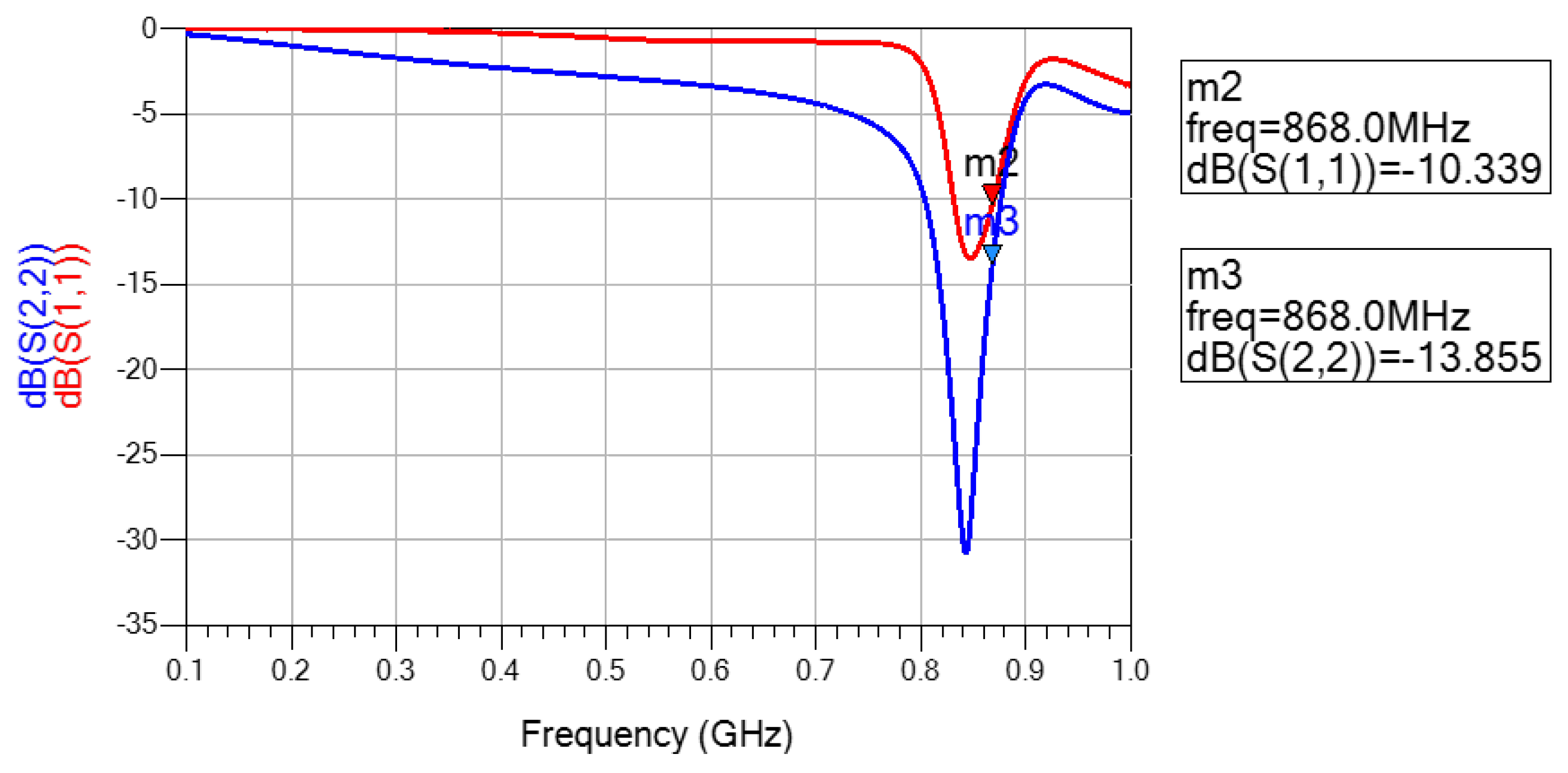
3.3.1. Impedance Matching
As mentioned in
Figure 5,
and
determine the input and output reflection coefficients. They indicate how well the LNA is matched to the source and load 50 Ohm impedance at the 868 MHz design frequency band of interest. Accordingly, input and output return losses
and
, respectively, have to be kept below 10 dB for fewer reflections and maximum power transfer. If the device has a poor output match, mismatch errors will degrade the whole LNA performance [
31].
In the adopted architecture, the match is designed in the input port by combining two capacitors in the series and directing one inductor to the ground. In the output, the lumped component chosen for the matching is a capacitor, the inductor in the series, and one capacitor in the branch is matched to the ground. The matching system is verified using an S-parameter chart in ADS as shown in
Figure 6. At 868 MHz,
dB and
dB.
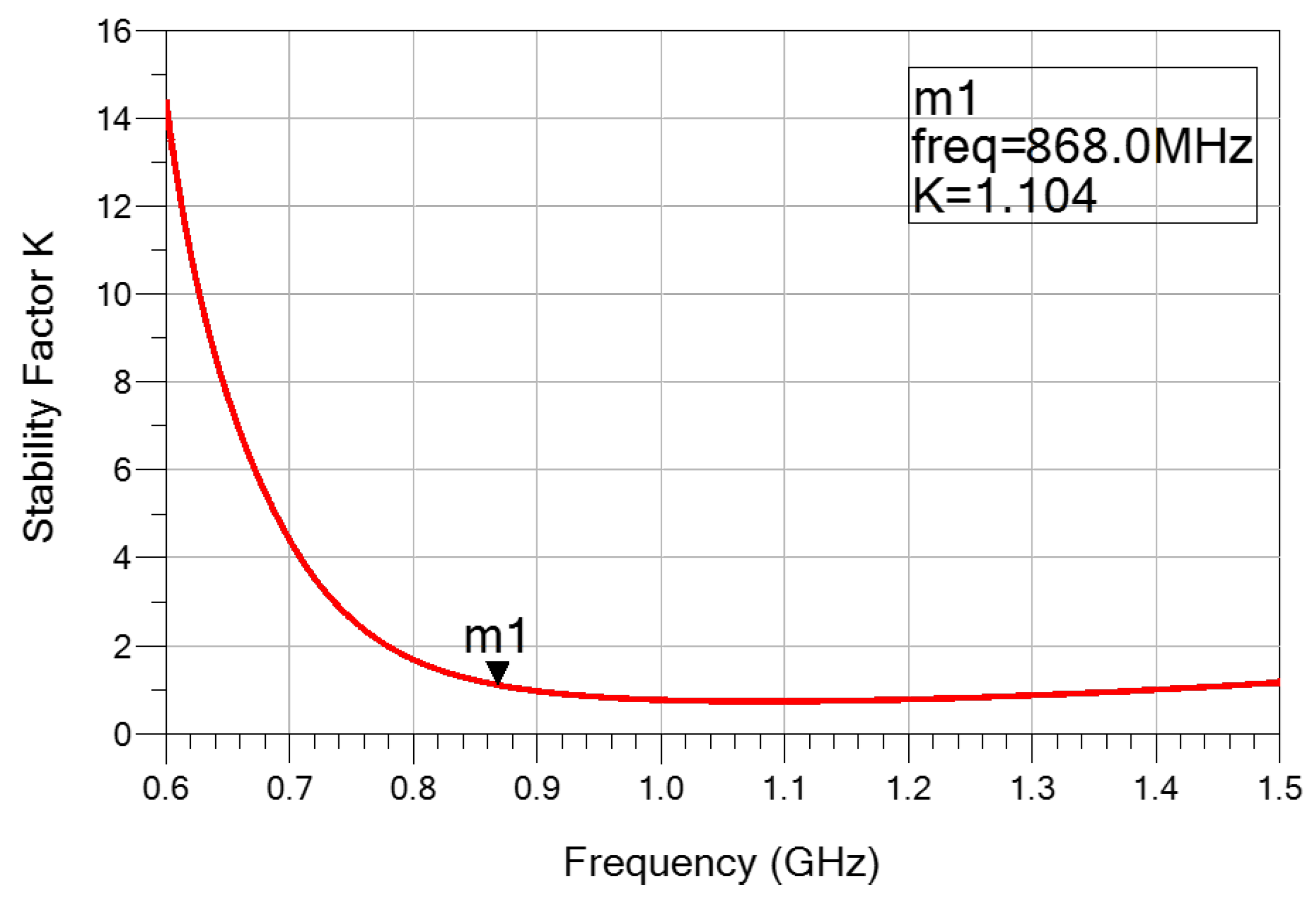
3.3.2. Stability
Stability is also a critical parameter used to determine the correct behavior of any amplifier. The main goal in designing the RF amplifier is to have an unconditionally stable circuit within a specific operating frequency to avoid turning it into an RF oscillator. The calculation of the Rollett stability factor (K-factor) using S-parameters derived from the simulation or from the hardware measurements is a common method by which to determine the stability of the designed system.
When
and
, the LNA is said to be unconditionally stable [
31]. This is also called the small signal stability test, which is valid for a specific bias and frequency point. Therefore, the input and output ports are matched and the LNA is stable as described in the impedance matching section.
During the simulation, the stability of the circuit was verified at an early stage together with the matching phase. To ensure the stability of the amplifier over a wide range of frequency points, the factor
K was tested on ADS with a frequency sweep of 0.5–1.5 GHz. With any tuning or value changes in the architecture, K is kept larger than the unity as shown in
Figure 7. The circuit is stable and facilitates any connection to the passive elements at input and output ports. Additionally, a feedback loop analysis is run after every simulation phase; if
K is less than one, the last modifications are reinitialized to avoid the transistor generating unwanted distortions or the circuit turning into an oscillator.
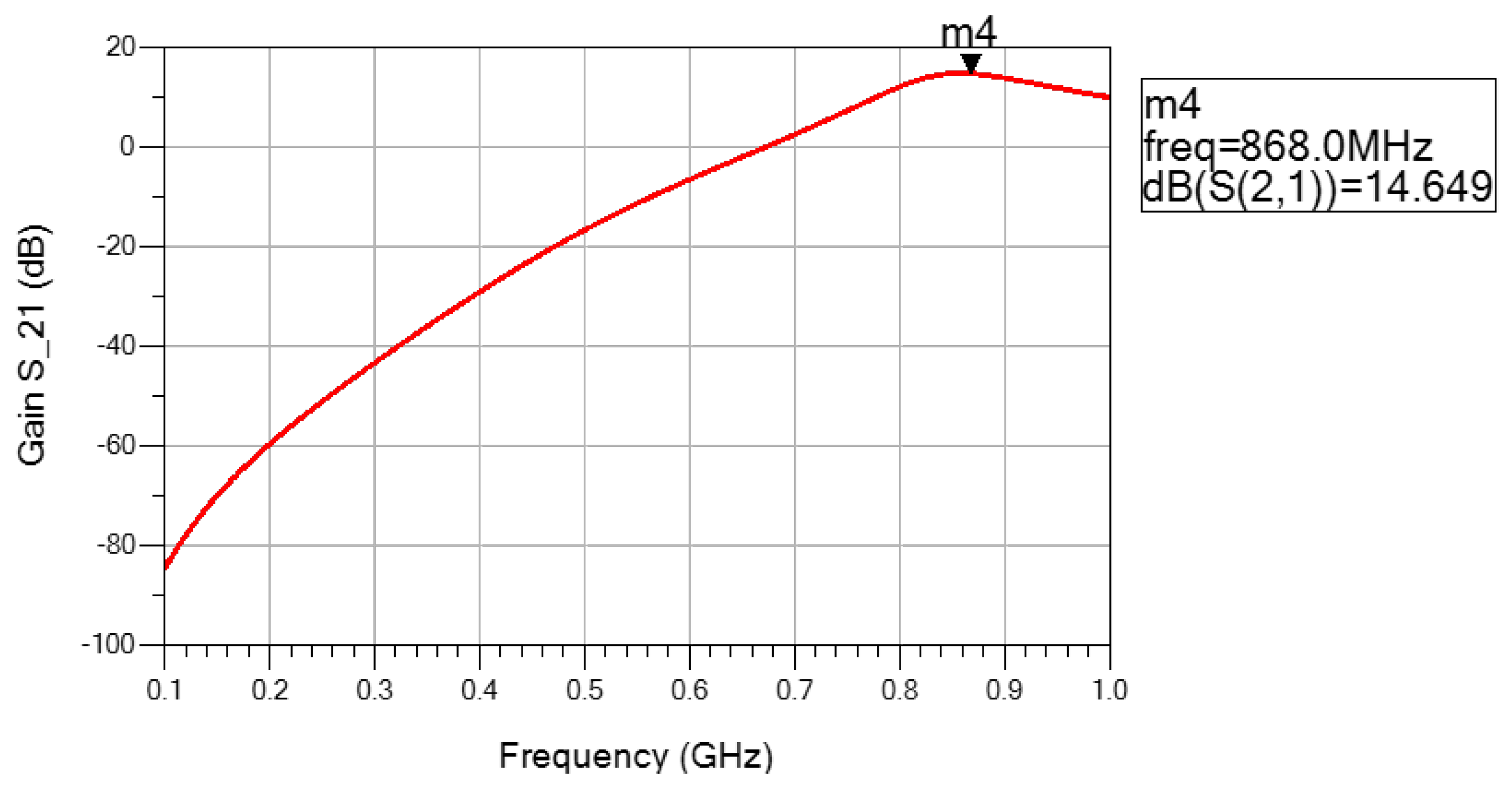
3.3.3. Gain
Theoretically, the gain is expressed in different ways as the transducer power gain, available power gain, and operating power gain. The main goal of the LNA design in the radio receiver is to amplify the incoming weak signals from the antenna and forward them to the rest of the circuit. Generally, the gain is the ratio between the output power of the LNA and its input power.
The Equation (
3) indicates that the transducer gain
is the ratio of the load impedance
and source impedance
[
31]. Furthermore,
is expressed as function of S-parameters with
=
, which are, respectively, the reflection coefficients associated with the source impedance and the load impedance. When the two ports are connected to a source and load with impedance
, the result of
=
= 0 and the gain is expressed as the square value of
In the literature, the gain level varies with the transistor and cascaded stages in the adopted architecture. The typical COTS LNA available in the market offer a gain level of up to 20 dB together with a low NF, but with a higher power consumption level, which does not match with the requirement of duty-cycled WuRx. With the designed prototype, the gain will reach a comparable level to that of the state of the art and also an ultra-low current consumption performance.
Many simulations were run to extract the best trade-off between gain and power consumption for the single and dual stages of the design. The implemented architecture of
was simulated as 14 dB gain, as mentioned in
Figure 8.
Table 3 presents other
levels simulated with the tuning of voltage supply for other optimizations through hardware tuning.
3.3.4. Current Consumption
Current consumption is not related to a specific formula for an LNA design. The selection of passive components in the designed architecture results in feedback on the power consumption of the whole circuit. The LNA is designed to be placed in a duty-cycled WuRx node. Thus, the need for the lowest possible consumption of LNA should be maintained relative to the power need of the whole WuRx circuit. The comparison between LNA designs in the SoA and commercially available prototypes identifies a range in consumption for the LNA design of around 1–2 mA for a single stage.
To achieve the minimum power consumption, the total current derived from the circuit was calculated using the current probe in ADS mounted in a series with the resistor R1 from the mentioned architecture in
Figure 4. The supply current was simulated by tuning the supply voltage, and an increase in gain with each successive voltage level was observed.
Table 3 shows the simulated results. The obtained results for current and gain performances under different supply voltages are kept for further applications that require a higher communication range and to consolidate increased power consumption.
3.3.5. Noise Figure (NF)
The NF is also an important parameter that should be considered in the design, especially in designing a multi-stage cascaded amplifier. The noise of the LNA design should be minimized to avoid affecting the system sensitivity and to enhance further stages. Friis’ Formula (
4) explains the calculation of the NF of a cascade of stages, each with its noise factor and power gain (assuming that the impedance is well matched at each stage).
and in the formula are, respectively, the NF and the gain for each stage.
NF is the practical noise figure of an RF network, NFmin is the ideal noise figure of a circuit and Mnf is the matched network factor.
The LNA’s NF should be kept as low as achievable to avoid affecting the overall system sensitivity. The lowest NF is not always found at the characteristic impedance or at the conjugate match impedance that maximizes the gain. When conjugally matching the source impedance with an optimum impedance, the LNA has the lowest NFmin. In most cases, the input of an LNA will be matched for the minimum noise figure, which may result in a mismatch in terms of power performance. Increasing the biasing current for improving stability could also amplify the parallel current noise source, which will lead to undesirable behavior of LNA. Tuning and simulating light intervals can maintain the desired design performances without external distortions and noise.
An NFmin must be at its minimum, with the bias point of LNA selected to be around 1 mA.
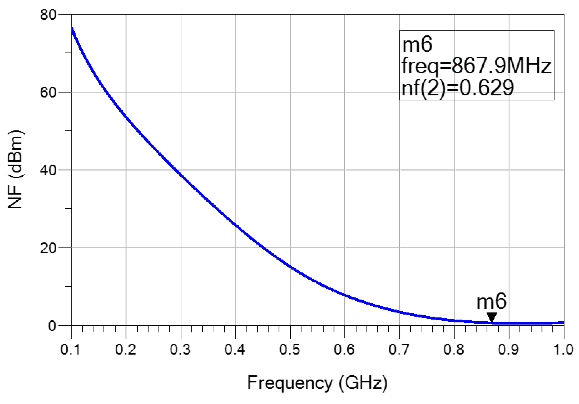
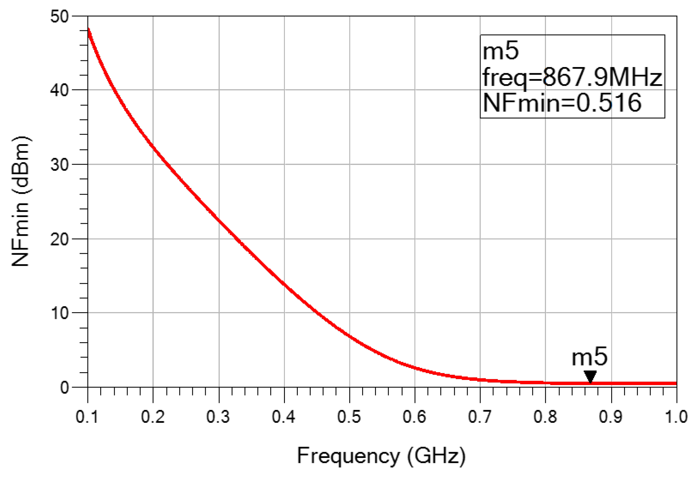
Figure 9 and
Figure 10 show the minimized NF performances for the proposed design at 868 MHz and at a low bias current for the operating transistor. NF = 0.629 dBm and NFmin = 0.516 dBm.
3.3.6. Linearity
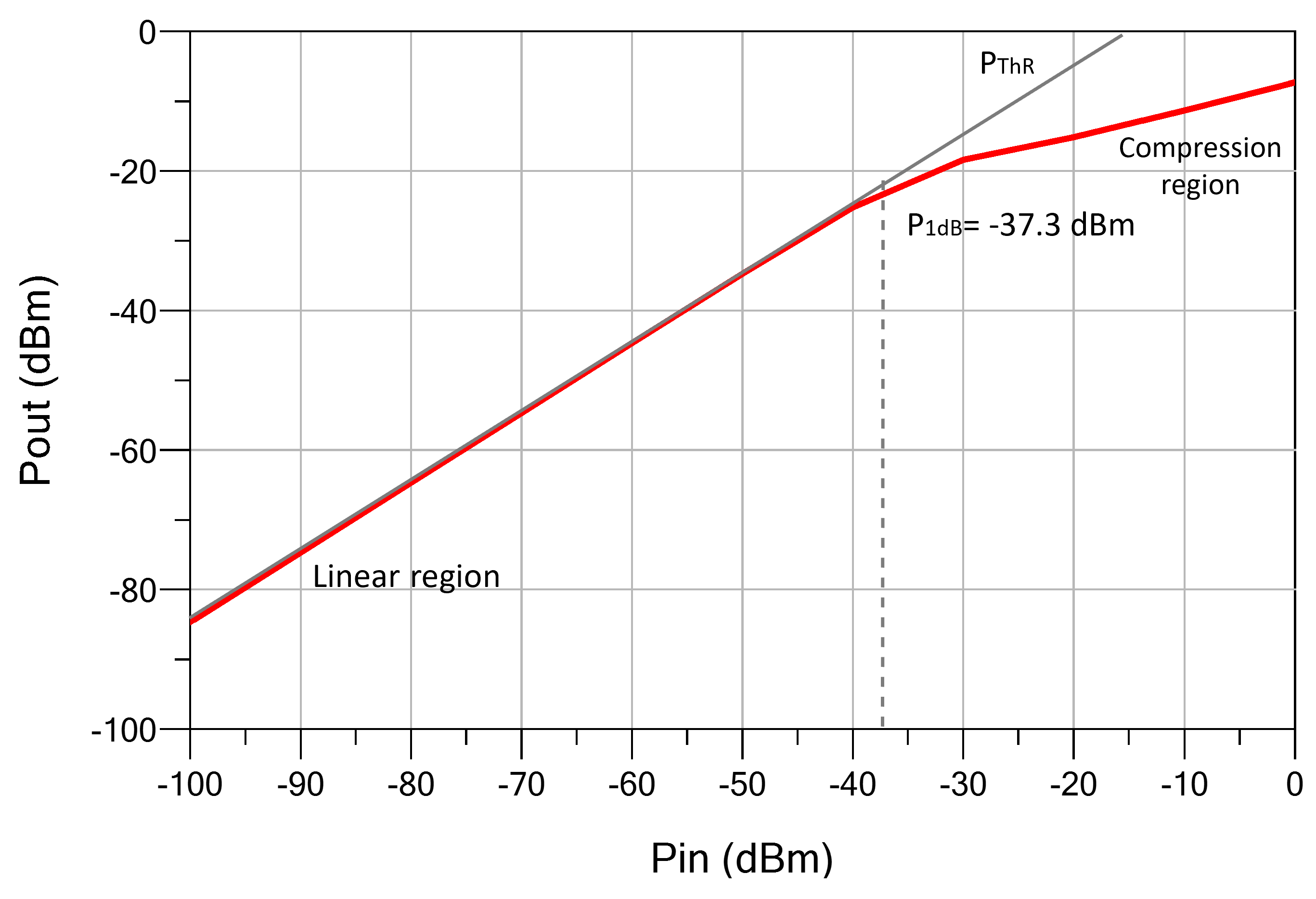
The investigation of LNA linearity requires the interpretation the gain compression and inter-modulation distortions against different input powers [
29]. The 1-dB compression point (
) is the output power level at which the gain decreases by 1 dB from its constant value. The Equation (
5) explains the estimation of the 1-dB compression point from the difference between the theoretical linear power
and
It is necessary to characterize the former in order to estimate the input power at which compression and distortions begin. For this purpose, a linearity analysis is extracted from the ADS simulation as shown in
Figure 11. The linear region for the LNA is below −37.3 dBm, which is acceptable for the adopted approach.
3.4. Trade-Offs between LNA Parameters
As described in the previous subsections, all the design parameters, such as stability, matching, linearity, consumption, noise figure, and gain, are equally important. To maximize the performance of the design, inevitable trade-offs should be considered, especially when RF components are highly sensitive, and a variation in some parameters could disturb the behavior of others [
31].
Some parameters have priorities. For example, stability should never decrease below 1 so as to avoid an unstable circuit. In SoA, a placement of resistor load at the output of LNA has the role of improving the stability but can decrease the 3 dB level from the gain scale, which is not tolerable in this application.
Those consequences were detected during the simulation of the circuit. In this case, the decision is to eliminate the resistor at the output to avoid decreasing the gain. Additionally, careful tuning is reacquired to keep the k factor of stability greater than the unity.
Moreover, the output matching network of LNA is usually designed to achieve maximum gain using conjugate matching. Simultaneously increasing the demand for the high linearity of LNAs, the trade-off between good compression points for better linearity and high gain must be considered. The linearity is an essential aspect for the on–off keying (OOK) modulation that will be adopted in the WuRx nodes. On the other hand, gain and power consumption should be treated simultaneously. For example, the variation of resistor values in the collector branch could improve the gain slightly but increase the current of the whole circuit.
Additionally, the RF amplifier related to the Friis Formula (
4) will introduce some additional noise by increasing the gain level and additional cascaded stages. There are other methods for minimizing the LNA noise by choosing low noise components, operating points, and circuit topologies. At this point, it is also mandatory to maintain a balance between all design goals such as power consumption and impedance matching.
The cost is also among the most important trade-offs that should be taken into consideration. During the selection of the lumped component or the printing process, a caparison is continuously taking place and the value for cost is considered. Furthermore, after comparison to the LNA design architectures in the SoA, a design process using off-the-shelf and lumped element was selected to save both time and cost, as the integrated CMOS technology have a higher processing time and design expenditure.
To conclude, the LNA designed for duty-cycled WuRx imposes specific criteria and trade-offs between these parameters. Therefore, the primary important design task during the simulation is to have multiple considerations to prepare for the hardware phase, which is typically very sensitive in RF.
4. Hardware Implementation and Measurement Results
4.1. Challenges of LNA Printed Circuit Board (PCB) Design
After running many simulations on ADS and extracting the best performances of the circuit, the hardware design still has multiple challenges and requirements that should be carefully considered. The transitional phase first uses electromagnetic compatibility (EMC) simulations to connect the simulation world to the real one. Generating such advanced EMC simulations did not prevent certain complications, which were treated by manually tuning some of the components. Hence, the advantages of the off-the-shelf design are the ease of reparation and corrections, and the accessibility to any desired improvement. The design phase was treated carefully to ensure a robust and reliable behavior for RF components assembled for the implementation. The layout is worked out using Altium designer as an advanced designer tool. Many competencies in hardware designing characterize this phase because RF board stack-up requires attention to details such as isolation between traces and components, several PCB layers and arrangement, power supply decoupling, placement of components, etc.
Additionally, an adequate calculation of RF traces in which the incoming signals propagate could lead to transmission losses and interference issues. A ground plane is placed below the layer to make the current flow path as short as possible with the introduction of parallel vias to reduce the parasitic effect of capacitance and, therefore, to reduce the interference at 868 MHz frequency [
32].
4.2. Hardware Testing Process
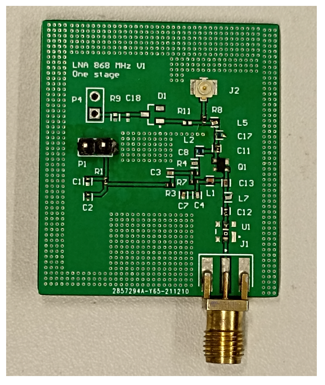
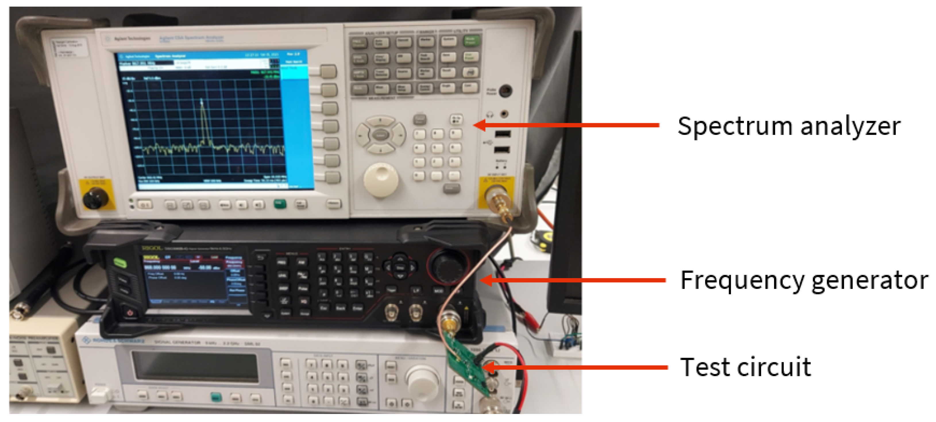
Hardware testing is usually performed in the transition phase between the simulation and emulation of the implemented PCB. For example,
Figure 12 shows a single-stage LNA implemented under the first testing phase. For the LNA design, testing is needed to ensure that every circuit component performs well according to the specific requirements. The first testing setup is to verify the operating point of the transistor by measuring the current flow and base and collector voltage.
The amplifier gain was measured by feeding the LNA with a frequency generator and measuring the output with a spectrum analyser. The compression point and the linearity were measured by this setup too.
Figure 13 shows the measurement setup. The measurements will determine whether there exists adequate behavior within the circuit.
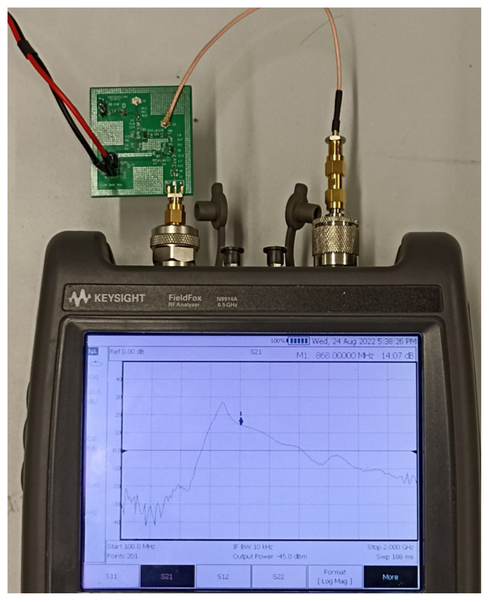
The final step in testing is the identification of the S-parameters using the Vector Network Analyser (VNA) as shown in
Figure 14. The VNA was configured with its minimum output power
= −45 dBm.
4.3. Hardware Measurement Results
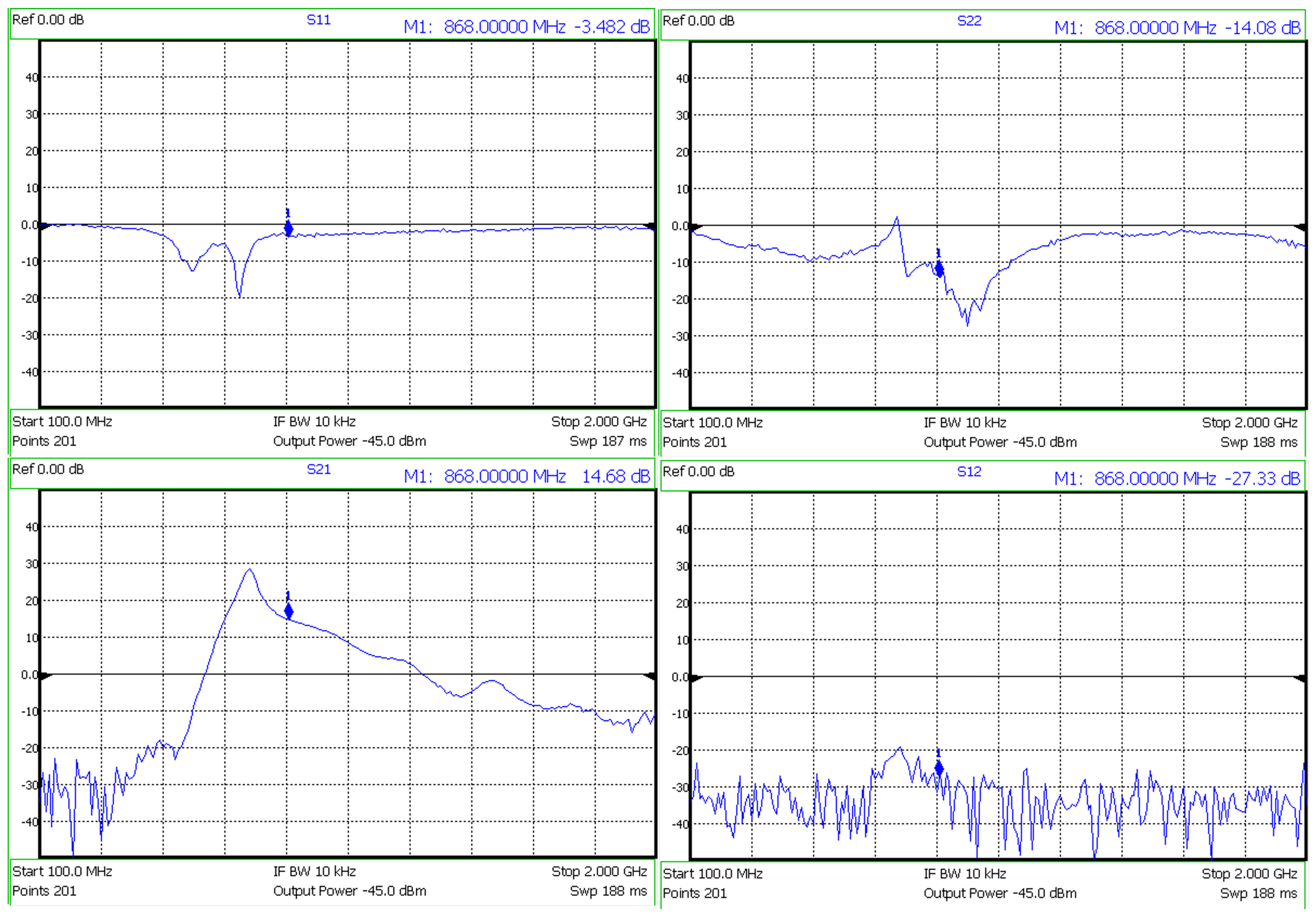
4.3.1. S-Parameters Measurements
As discussed in the previous section, S-parameters were measured using VNA and determine the overall related performances. The measurement results are depicted in
Figure 15. The following measurements are the best obtained for matching input and output after many frequency shifts in the obtained values.
At 868 MHz, the return loss for the input port was measured as dB which is acceptable and did not affect the performance of the other parameters. The return loss for the output port was dB, which allows for a maximum power transfer for the envelope detector, which is placed after the LNA in the WuRx design. The value of is dB, which is a more powerful reverse isolation that eases the task of impedance matching and improves amplifier stability. Finally, the was measured as dB, which reflects a good result for one-stage amplifier gain.
The observation of S-parameters results at 747 MHz shows more promising values for and which reach, respectively, dB and dB. The results in this shifted frequency are the basis of future improvements aiming for a single-stage higher gain with better input impedance matching.
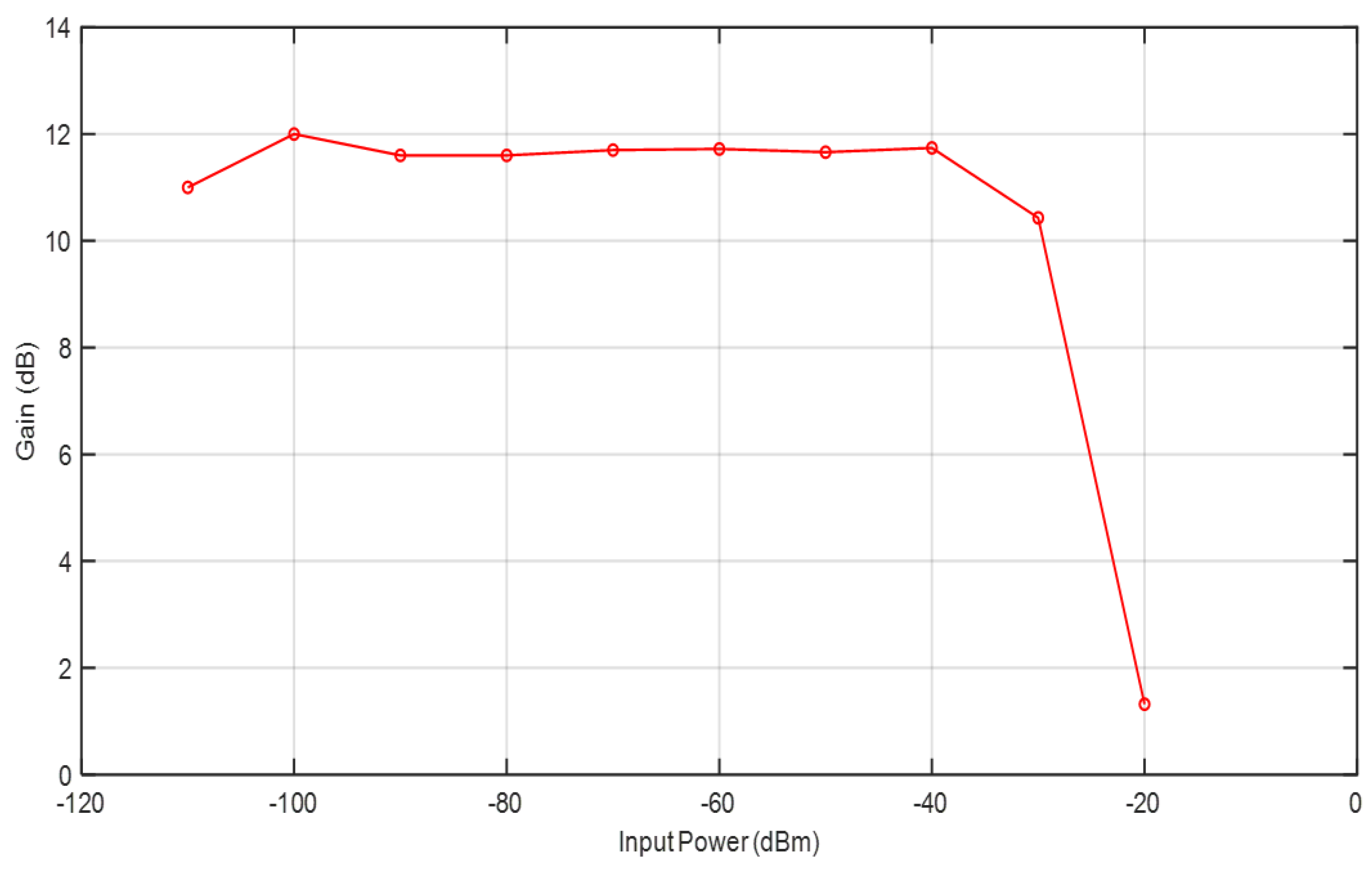
4.3.2. Behavior of Gain with the Variation of Input Power
The gain behavior with the input power variation at a fixed supply voltage was studied. Using a frequency generator in input enhances testing with very low input power to test the sensitivity of the front-end.
Figure 16 confirms that the gain is stable while varying the incoming power. This measurement setup also concludes the system’s stability and linearity within a lower power range.
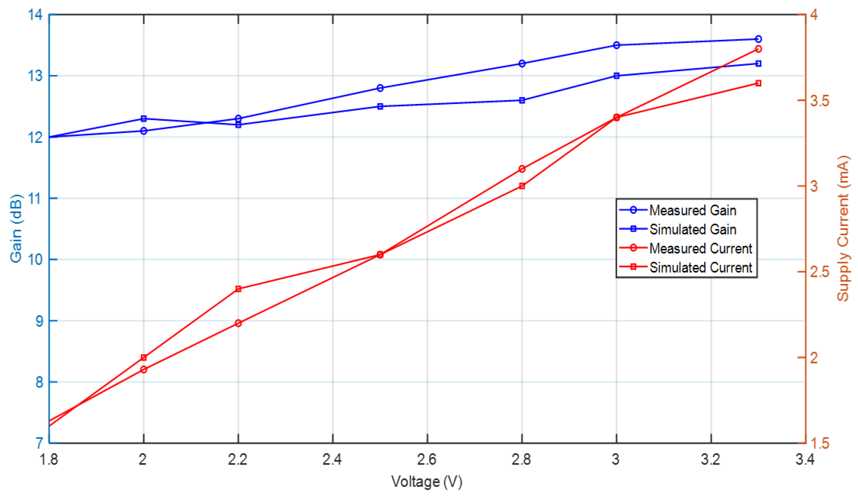
4.3.3. Behavior of Gain and Current with the Variation of Supply Voltage
As in the simulation phase, the supply of the LNA was tuned in the range of 1.8–3.3 V to extract all working states for the circuit and conclude the best parameters trade-offs.
The curves in
Figure 17 present both the simulation and measurement results for the gain and the supply current under the different voltage levels. The measurement results are very close to the simulation. For example, the gain indicates a slight increase where the current varies in the range of 1.8–3.5 mA.
This variation enhances the ability of the proposed LNA to work under different conditions and to serve different applications.
The decision of which supply voltage will be selected is related to the essential need for the duty cycled WuRx, which is the primary purpose of the LNA design. In addition to the need for ultra-low power consumption for this node, technologies deal with a moderate gain and avoid higher current levels. Furthermore, as the design is based on off-the-shelf technology, different architectures could be implemented for different wake-up-based applications.
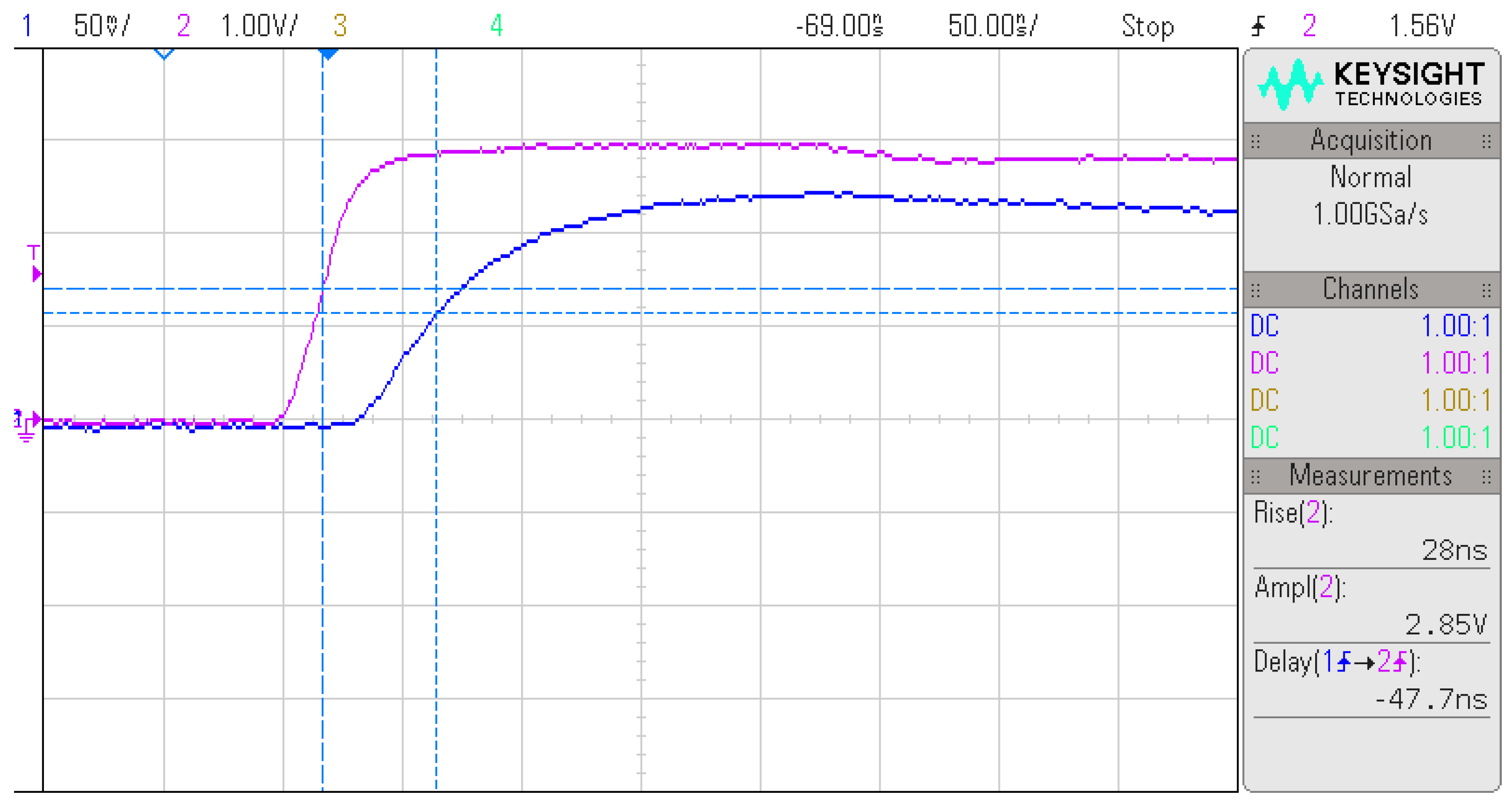
4.3.4. Settling Time Measurement of Low Noise Amplifier
As the LNA circuit is designed for duty-cycled WuRx nodes, the settling of the circuit seems an essential factor that should be taken into consideration among the other design criteria. A higher speed of LNA settling following turning on will be advantageous in integrating other wake-up blocks.
The whole process is based on the duty cycled approach. A long turn-on time will degrade the capabilities of the receiver. In the COTS LNA works, the settling time is not often mentioned, making this parameter comparison relatively harder.
The settling time measurement setup is achieved after mounting the output of the LNA with an envelope detector designed based on SMS7630 diode from Skyworks and matched for the LNA measurements purposes. The observed delay between the LNA signal and transient response of the supply voltage and the rectified signal are illustrated in
Figure 18. A delay of
ns can be observed between both signals, which is ultimately the settling time of the LNA. Compared to other LNA designs in
Table 1, the obtained turn-on time of the designed amplifier is a promising result for integration with the WuRx.
5. Performance Analysis for Duty-Cycled Wake-Up Receiver Based on Low Noise Amplifier
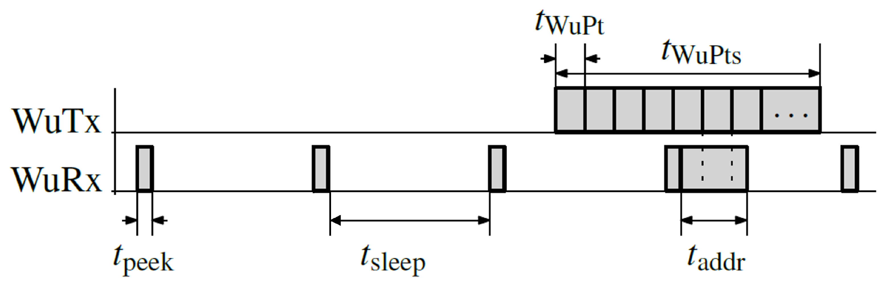
As described at the beginning of this paper, the WuRx is characterized by the continuous listening of the receiving channel, the identification of WuPt and the activation of the awaking signal of the main unit, which is the MSP430 micro-controller in this of this work. The duty cycling process is well structured, with defined periods for each communication phase.
The timing diagram in
Figure 19 explains the duty-cycled communication. The receiving phase is characterized by a peak in time which is reduced so as to be as short as possible to reduce the overall power consumption. The
is the necessary duration for detecting a wake-up packet, and
is the duration between two active phases. The transmitting phase includes the
, which is the duration of the signal wake-up packet for transmitting the wake-up address. The address decoding of the wake-up,
, needs to be at least twice the WuPt to ensure a complete reception of the address.
A timer configuration in MSP430 programming generates an interruption every to activate the wake-up. After the necessary time execution, if the wake-up signal detected is valid, the interruption is generated by the microcontroller, and the wake-up component is turned off again. When talking about scheduling the time of the reception process, it is mandatory during the design phase to ensure the fast settling time of the LNA. The duty cycled approach of the WuRx will be based on minimizing the active time of the receiver. The long settling time can be a factor that degrades the whole system design. The successful duty cycled approach is generally ensured only if the trade-off between energy consumption, latency, and sensitivity is considered.
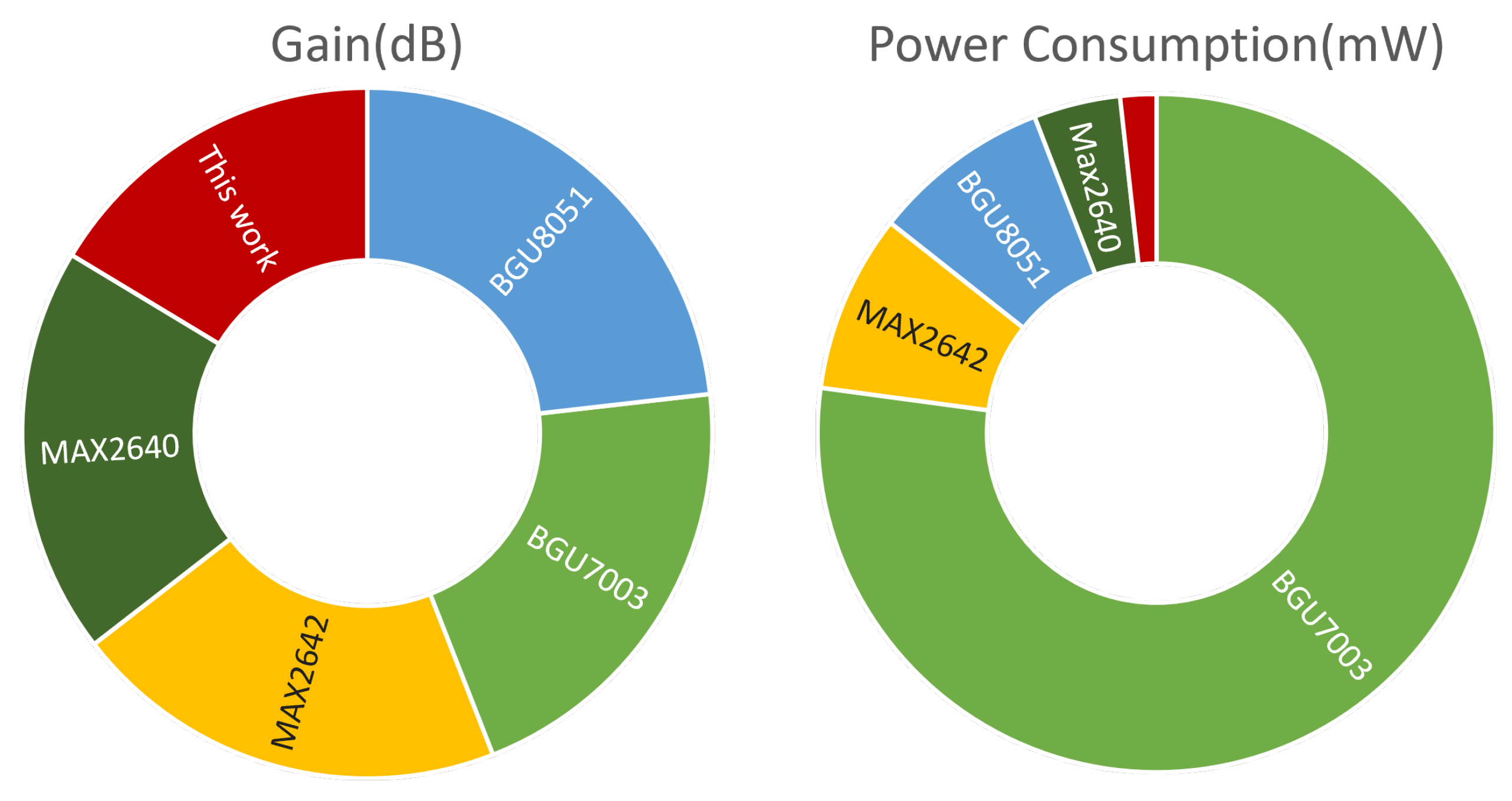
This section compares the results obtained from the designed LNA with other COTS LNA in terms of gain and power consumption. Then, the MAX2640 is selected and mounted on the same WuRx board to achieve an accurate sensitivity analysis based on the same envelope detector sensitivity and for a precise power consumption calculation of the overall system design.
5.1. Comparison with Commercialized Off-the-Shelf Commercialized Low Noise Amplifiers
The hardware measurements presented in the previous section satisfy the requirements for the designed LNA. For better performance analysis, comparing the LNA metrics with other designs in the SoA is mandatory. A comparison with other technologies operating in other frequency ranges, as mentioned in
Table 1, would not reflect the improved qualifications offered by this work. For validation, a comparison was made with the COTS LNA presented in
Table 2.
Figure 20 presents an observation of the amplifier gain and power consumption of this work toward the other works operating in 868 MHz. The gain level for a single design stage compared to the other COTS LNAs is at the same level. As the designed LNA offers a gain range of 12–15 dB at 868 MHz, which is the same as MAX2640 and MAX2642. Even BGU7003 and BGU8051 achieve the 20 dB gain; in term of power consumption, the designed LNA consumes five times less power compared to the MAX LNAs and twenty times less than the BGU LNA family. This enhanced the proposed design and helped to determine it as having the best design performance in terms of power consumption with the same gain level as the available COTS LNAs.
Finally, a notable investigation of the total circuit’s consumed power is obtained. Finally, the trade-off between those two parameters is determined.
5.2. Comparison of the Designed with the Commercial MAX2640 Low Noise Amplifier
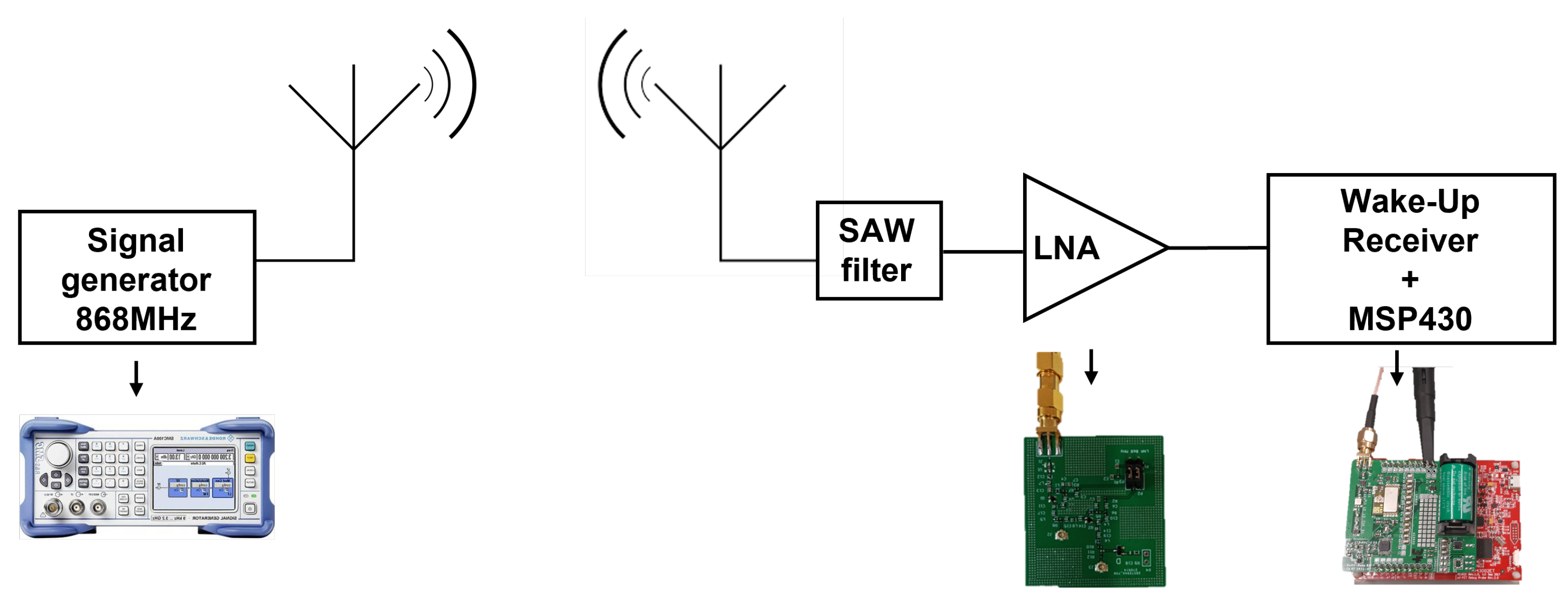
For the comparison, because relating the extracted parameters from datasheets could sometimes be misleading, the idea was to compare the designed LNA with one of the COTS LNAs mounted in a duty-cycled WuRx front end. For this observation, MAX2640 LNA is matched to the hardware design of duty-cycled WuRx. The demonstration of the wake-up implementation and the overall approach for successful wake-up packet reception is detailed in [
16]. For gathering packet error rate (PER) measurements and power consumption measurements, the overall system should contain a Micro Controller Unit (MCU) for data aggregation, which is the MSP430.
Figure 21 shows the measurement system design for implementing the duty cycled WuRx including LNA.
Table 4 shows the power consumption during the active state of the WuRx as well as the total current consumed during WuPt transmission, which includes both the active and sleep phase from the wake-up timing approach. The mean power consumed is identified according to the voltage supply of the circuit. As the used envelope detector implemented in the designed WuRx is limited with a
dBm sensitivity, the whole circuit based on MAX2640 reached a
dBm sensitivity when consuming
μW.
To summarize, the whole measurement setup, the overall system, including the designed LNA, reaches dBm and consumes μ when supplied by V. For the same design, when it is powered by V, it achieves a lower sensitivity level dBm with a promising result in the total power consumed, which is μW.
6. Summary
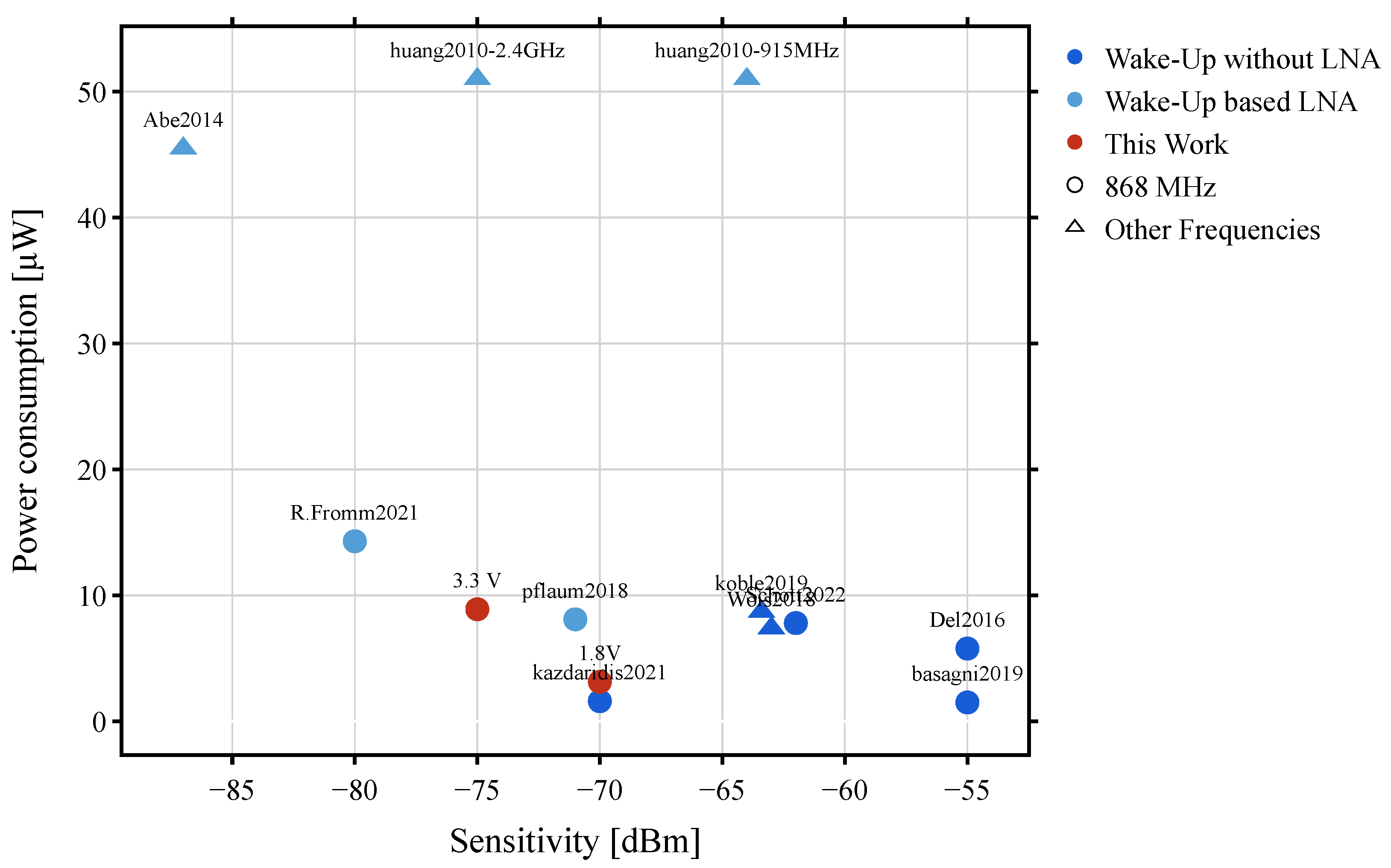
Based on the measurements resulting from integrating the designed LNA into the architecture of the duty-cycled WuRx, it is mandatory to compare with other wake-up works either in the same frequency or in other bands based on other architecture. The reason behind this is the lack of similar works in the SoA which enhance the particularity and exclusivity of this work in such a new field of research.
Taking into consideration the two main axes, which are the sensitivity and power consumption at 868 MHz, the developed work, as mentioned in
Figure 22 shows lower power consumption with sensitivity levels of up to
dBm. Furthermore, depending on the supply voltage and the tuned values used to select the desired performances, lower sensitivity is also accepted with
µW consumption for the whole circuit.
In the same chart, other references are indicated, citing the approach of [
33,
34], and they exceed the amount of power specified, which is not adequate for WuRx designs. Additionally, refs. [
35,
36,
37] used technologies that are integrated or off-the-shelf designs, which are limited to possessing low sensitivity levels [
38,
39,
40,
41], which does not provide a good communication range. The present work provides the optimum trade-off between power consumption and gain among the other WuRx architectures.
7. Conclusions
In this paper, a recent research field is investigated, i.e., the adoption of WuRx nodes in the wireless communication area. Due to the receivers’ importance in energy efficiency, it is important to conduct investigations for its behavior improvements. Improving the sensitivity of sensor nodes is a concern of the work presented in this paper.
Improving the sensitivity in a front-end antenna while keeping the overall circulating current as small as possible is a challenging task. The critical factor to success in this regard is to consider the overall of design performances and find a way to achieve the desired specifications. Specifically, the purpose is to achieve the highest gain level with the lowest power consumption possible. Other design performances such as stability, linearity, the noise figure, and input and output matching are taken into consideration in the overall design phase.
The BFP740 bipolar junction transistor (BJT) was selected as an active device for amplification in a CE architecture set in an ideal operating range. The circuit is implemented with commercial off-the-shelf components due to the availability, low cost, flexibility, and ease of implementation, from considering basics in determining LNA design performances to running multiple simulations on ADS.
The benefit of simulation is extracting the strange behavior of the signal in the time domain, verifying the stability and matching of the impedance port, and tuning the lumped component to extract the best trade-off between gain and current consumption. Despite this, the simulation phase required modifications and improvements, and the hardware implementation phase presented plenty of challenges. Many soldering problems were faced, especially in the fine-tuning of some values and frequency shift problems due to the sensitive RF component and the high operating frequency band. Moreover, the results obtained from a single design stage are convincing, and the placement of the proposed design among the COTS LANs demonstrates an impressive result in terms of power consumption.
Finally, the integration of the design with duty-cycled LNA and the comparison with MAX2640, and with the whole front-end design, reveal the investigation prospects of the proposed design.


