1. Introduction
Over the last few years, there has been a strong increment in internet traffic. This led to a rising interest in high-speed wireline communication systems with ever-increasing data rates, especially in data center applications. As of now, the most employed modulation in SerDes transceivers is Pulse Amplitude Modulation with four levels (PAM-4) [
1,
2,
3], which allows doubling the data rate using the same symbol rate compared to Non-Return-to-Zero (NRZ) modulation. To achieve even higher data rates, the symbol rate of the system can be increased, but this approach is limited by the bandwidth of the channel. To overcome this problem, a higher-order modulation can be used. Examples of these modulations are PAM-8 [
4,
5,
6], and other eight-symbol modulations such as [
7] that increment the data rate by
compared to PAM-4, while using the same symbol rate.
On the other hand, PAM-8 introduces other challenges. Indeed, due to the high number of voltage levels required, it is much more sensitive to non-idealities such as noise, non-linearities, and Inter-Symbol Interference (ISI) that reduce the eye aperture. This directly affects the Bit Error Rate (BER) of the receiver, reducing the performance of the overall link. While the noise can be theoretically reduced by increasing the power consumption of the analog front-end and the ISI can be compensated by more complex equalization techniques, the non-linearities are difficult to address. Due to the low supply voltages of scaled CMOS technology nodes, it is challenging to achieve a high voltage swing for a good Signal-to-Noise Ratio (SNR) while maintaining a suitable total harmonic distortion (THD).
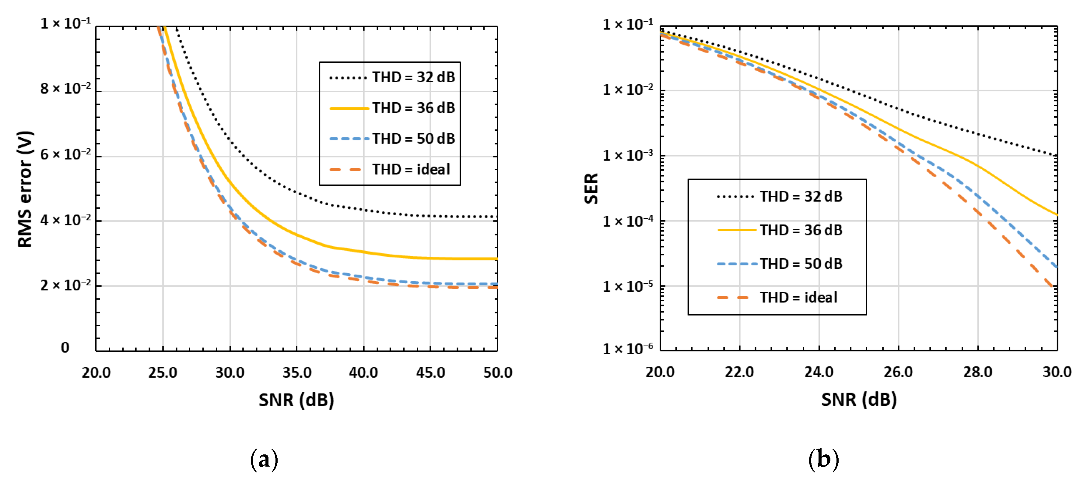
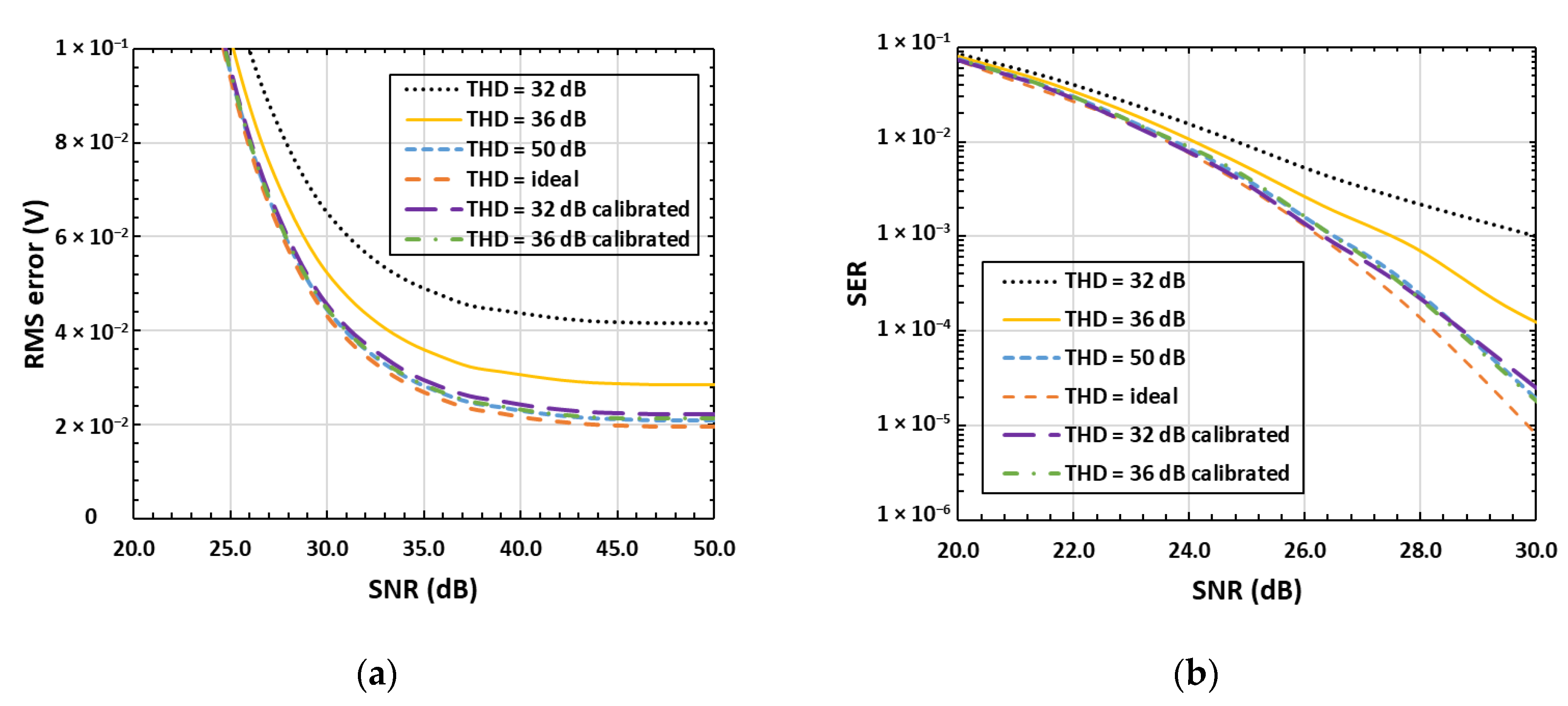
Figure 1a shows the simulated root mean square (RMS) error at the slicer input, including the contribution of noise, residual ISI, and distortion, as a function of SNR (due to additive noise at receiver input) for different levels of receiver (RX) static THD derived using a MATLAB simulation of a PAM-8 receiver. For THD values of approximately 32 dB and 36 dB [
3], as used in typical PAM-4 receivers, the system shows a higher value of MSE compared to the 50 dB case which resembles the error in the case of an RX with ideal linearity. The same behaviors are visible in
Figure 1b where the SER was obtained for a lower range of input SNR. This range was used to give evidence of the system behavior while not having to perform time-consuming simulations which can give a statistically relevant number of points to calculate the SER for high SNR values.
Because of the difficulties in achieving a high THD, the need arises for calibration to maximize the linearity, especially for the track-and-hold (TH) sampling stages of time-interleaved (TI) ADCs commonly used for wireline receivers. Indeed, as these blocks typically work with a large signal swing to maximize ADC loading, they are a significant contributor to overall THD. While many techniques can be found in the literature to reduce the non-linearities introduced by the TI ADC interleaving mismatches [
8,
9], there are relatively few examples of systems that address the non-linearities of the analog front-end. In [
10,
11], such systems make use of complex algorithms in the digital domain.
This paper proposes a TH circuit with tunable non-linearities and a simple calibration loop that allows maximizing the static linearity of the analog front-end by controlling a bias voltage in the analog domain. This could either improve the BER of the receiver or relax the constraint on the SNR for the same value of BER required.
2. TH Sampler
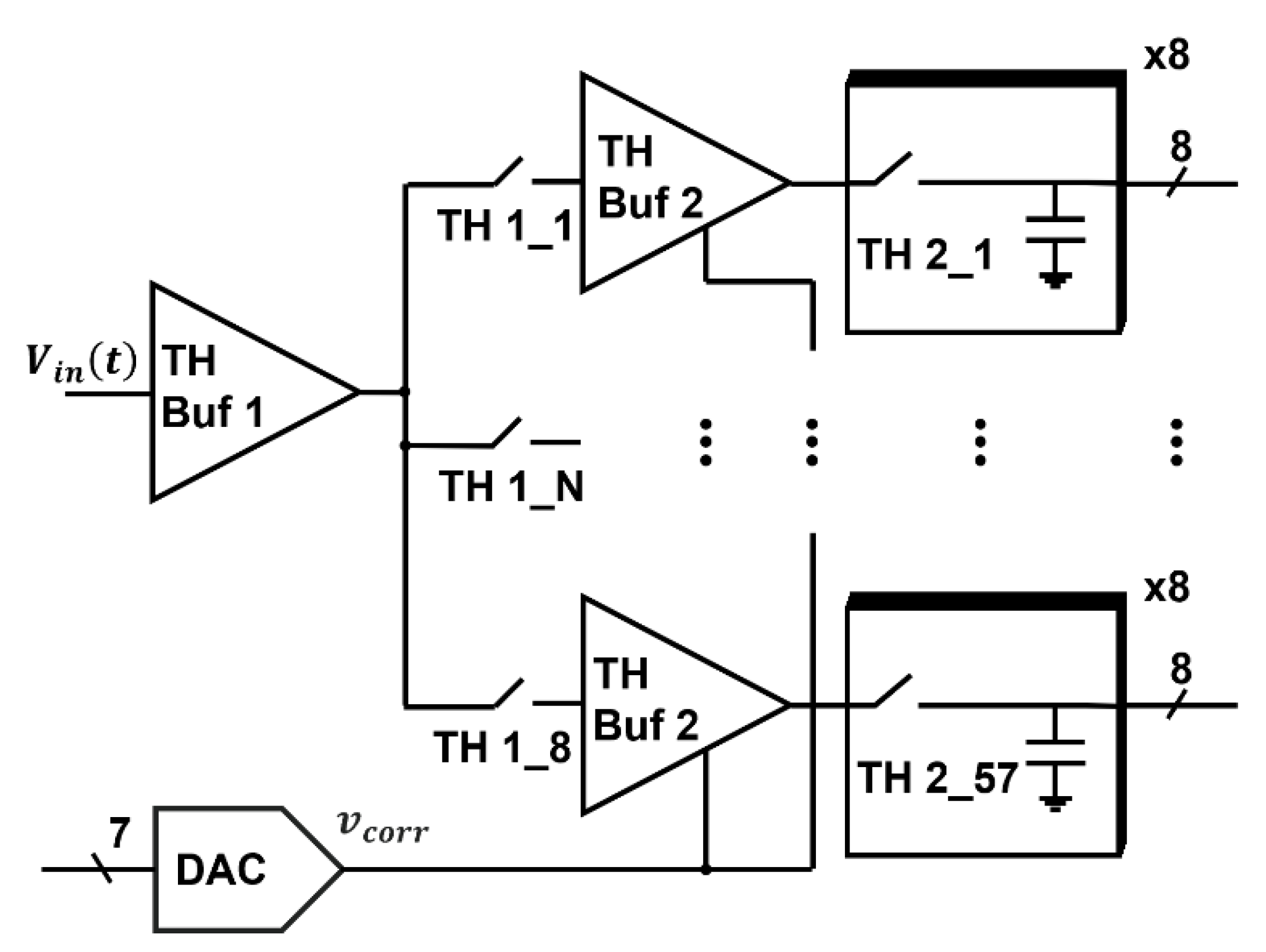
Figure 2 shows the top block diagram of the TH sampler. The circuit samples the input signal on 64 TI capacitances with a sampling speed of
. This is achieved through two cascaded time-interleaved stages. The signal is first sampled on eight different capacitances by the first stage, and then this process is repeated by the second stage for each of the eight sampled values. The sampling speeds of the two stages are 7.5 GS/s and 937.5 MS/s, respectively.
2.1. Circuit Description
The first stage is implemented through the sampling buffer described in [
12]. In the second stage, eight interleaved buffers are used. Each one is followed by eight time-interleaved sampling switches to reach the desired interleaving factor, equal to 64. These eight buffers must support an input common-mode around half of the supply voltage to accommodate the output common-mode of the previous stage. Suitable solutions are the ones used in [
13,
14], which are
gm-gm inverter-based topologies. These topologies are very simple to design while having good speed and linearity.
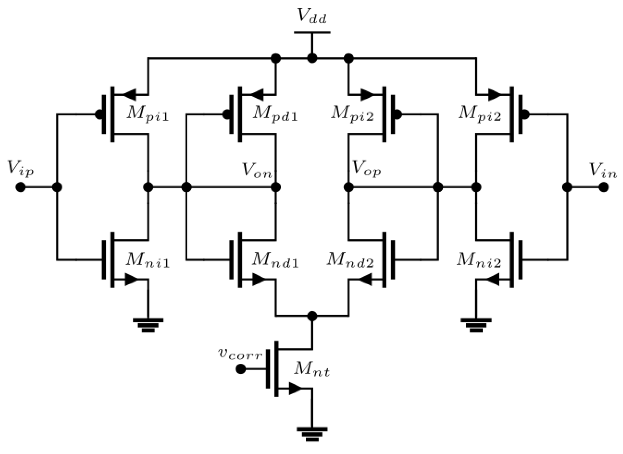
The linearity performance of this circuit stems from the opposite behavior of the inverter and diode. While the inverter compresses the signal, the diode load provides decompression. These two effects tend to cancel each other, resulting in overall good linearity. Nonetheless, this solution shows some limits due to the imperfect matching of the non-linearities. This is especially true across process corners and temperatures in which the behaviors of the inverter and the diode are significantly different, thus reducing the linearity.
For this reason, the solution shown in
Figure 3 is proposed. It consists of a simple inverter for the first
gm stage, followed by a differential current-controlled inverter closed in a diode configuration as load. The gate voltage
of the tail transistor
can be tuned to change the non-linearities of the diode and cancel the transconductor ones.
2.2. Second-Stage Buffer Linearity Behavior
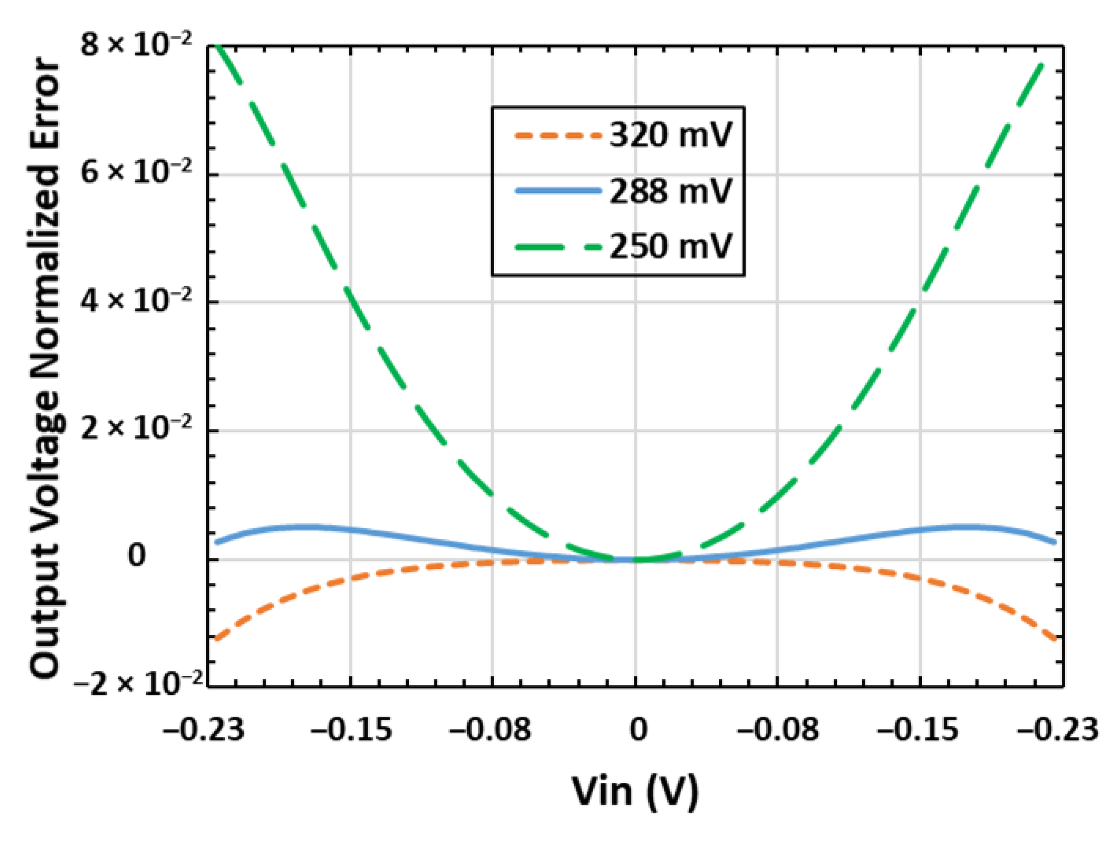
The relative non-linearity error (
εr) of the buffer static input–output characteristic is defined as follows and it is shown in
Figure 4 for different values of
:
where
and
are the output and input differential signal, respectively, while
is the linear gain of the buffer.
The transfer function of the second stage can be made linear, compressive, or decompressive depending on the value of the bias voltage .
The value of
which maximizes the linearity of the buffer across temperature and process corners is shown in
Figure 5. The optimum has the same trend with temperature, but the temperature coefficient may be quite different for different process corners. A bias circuit that allows the buffer to work in the optimum condition across PVT is thus not straightforward, and hence a calibration is required.
Another observation is that through the correct choice of the second buffer bias point, the non-linearities of the previous or successive stages can be compensated for. To perform this operation, a calibration is required to identify the non-linearity of the analog chain and find the correct value of . This allows maximizing the THD performance of the overall analog front-end.
3. Linearity Calibration Loop
The actual implementation of the linearity calibration loop strongly depends on the system in which the TH circuit is implemented. In this paper, the circuit is employed in a PAM-8 receiver, and a calibration feedback loop suitable for such receivers is presented.
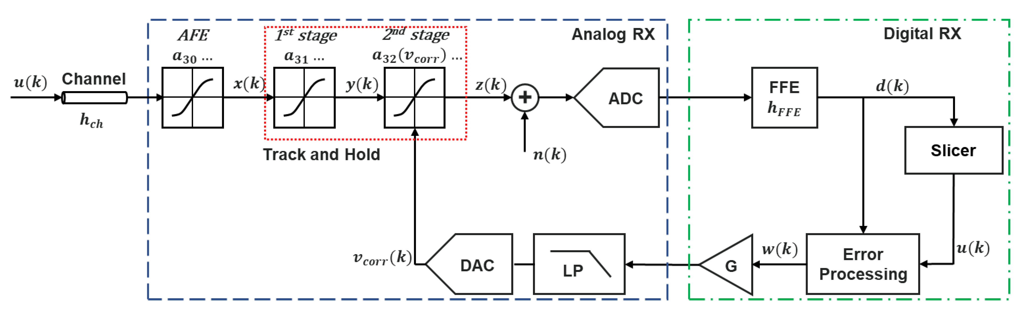
A PAM-8 receiver can be represented using the block diagram in
Figure 6. The channel symbol models the transmitter filter, the transmission channel, and the analog front-end of the receiver using their combined impulse response (
hch). The non-linearities of the AFE are modelized in the subsequent block. The transmitted symbols filtered by
hch are then fed to the TH, which is composed of two stages. The non-linear input–output characteristic of the circuits will be described by the coefficients of a Taylor approximation in the developed model as discussed in the next section. Moreover, for the second-stage buffer, the coefficients are dependent on the value of
.
After the second-stage buffer, the equivalent noise of the receiver is added to the samples and the signal is quantized by the ADC. A Feed-Forward Equalizer (FFE) is then used to remove the ISI introduced by the channel. Finally, the slicer makes the hard decisions given the soft decisions as its input. By the proper digital processing of soft and hard decisions, information about the optimum value of can be extracted in order to minimize the receiver non-linearity errors.
The ADC and the DAC used in this model are ideal. Typically, the ADC introduces non-linearities that are neglectable compared to the ones of the track-and-hold circuit, meaning they do not have great impact on the overall system. On the other hand, the DAC does not need to be linear as long as its input–output characteristic is monotone because the feedback loop will drive the DAC to the optimal value of .
3.1. Taylor Approximation Validation
The non-linear input–output characteristic of the second-stage buffer can be analytically described using the Taylor expansion. Neglecting the even terms due to the differential nature of the circuit, the following expression can be written:
where
is the linear gain of the buffer and
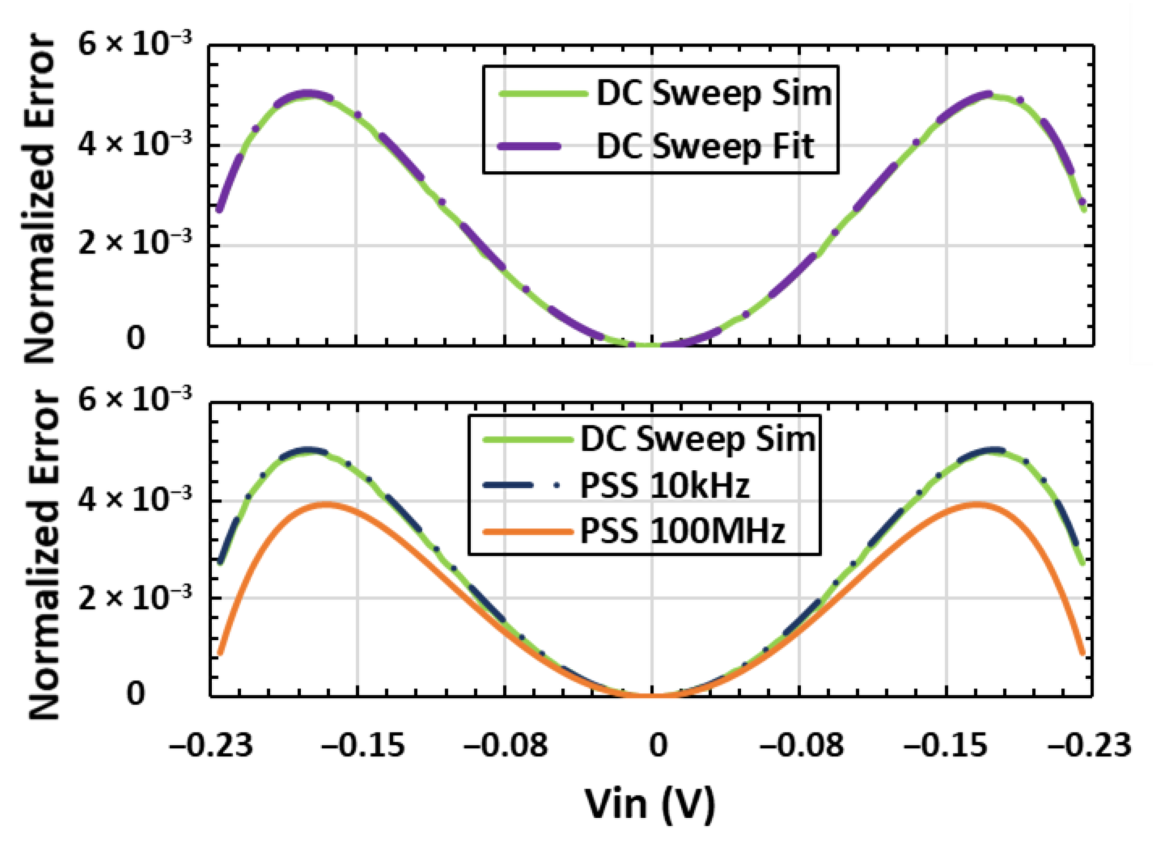
represents the odd-order distortion coefficients. To verify the validity of the analytical model, the relative non-linear error
of the second-stage buffer, obtained through a DC sweep of the input signal, is compared with a polynomial fitting of the characteristic with
i ≤ 3. As shown in
Figure 7, the Taylor expansion up to coefficient
a7 gives a good approximation of the non-linear error, as long as the input signal is included in the range between −220 mV and 220 mV. This corresponds to the maximum voltage amplitude allowed by the second stage.
The polynomial approximation is also verified for different input signal frequencies
Fin, performing Periodic Steady State (PSS) simulations of the second-stage buffer for
Fin =
and
Fin =
. From the non-linear output of the PSS simulation, the polynomial distortion coefficients
are calculated (with
i ≤ 3). The relative error arising from the coefficients is then compared to the DC sweep simulation (
Figure 7). For an input signal frequency up to 100 MHz, the Taylor expansion described above gives a good approximation of the non-linearities of the second-stage buffer. Higher frequencies were not considered because, as we will see in further sections, a DC characterization of the non-linearity still allows the system to converge to an optimal value of
.
3.2. Calibration Loop Operation
Indicating with
the PAM-8 symbols sent by the transmitter, the signal
at the first-stage buffer input is
. The signal
z(
k) at the TH output is then:
where
,
and
are the coefficients which describe the non-linearities introduced by the cascade of the two buffers and of every component of the AFE chain depicted in
Figure 6.
Assuming an optimal FFE, and thus a negligible residual ISI, the signal
d(
k) at the slicer input can be written as:
where
is the equivalent thermal and quantization noise of the analog circuit, which has zero mean value.
Assuming the slicer hard decision is equal to the transmitted symbol
u(
k), the following expression can be obtained by multiplying the slicer error
d(
k) −
u(
k) by
u(
k):
The resulting signal
w(
k) is multiplied by a gain G, low-pass filtered, and fed into a 7b DAC obtaining the correction voltage
. As the terms with zero mean value are suppressed by the low-pass filtering, the voltage
can be expressed in the first approximation as:
Therefore, the system can detect the non-linearity coefficients of the TH. The feedback loop will then set the value of
to minimize the error induced by such coefficients. The third harmonic of the input signal, whose amplitude H3 is proportional to:
is therefore minimized. This approximation can be obtained by sending a sinusoidal input signal with unitary amplitude
. Its Fourier transform can then be calculated after it is distorted by the sampling stages, obtaining:
By normalizing the coefficient of the third harmonic
, we obtain Equation (7).
In real applications, residual ISI is present even after the FFE. This means that the main cursor is not equal to the transmitted symbol value and therefore it cannot be canceled from the soft decision
d(
k) by subtracting the slicer output from it. To show this, we can first assume that
for simplicity, and define
, with
. If
is the impulse response element corresponding to the main cursor, the value of
is also dependent on the residual ISI component
that hides the non-linearities:
where
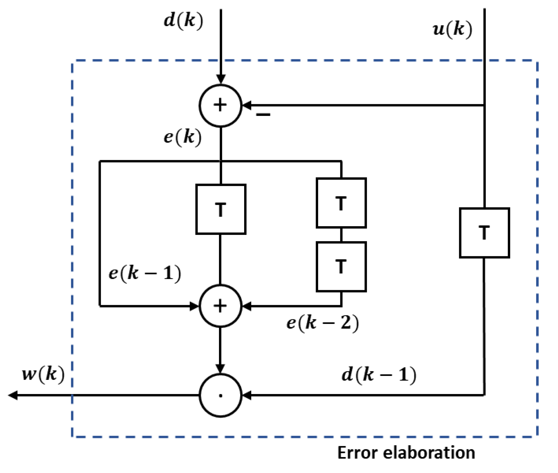
is a coefficient dependent on the channel and FFE. A possible solution to this problem is processing the signal with the method in
Figure 8. The errors of
successive and
previous samples are subtracted from
e(
k), removing the residual main cursor:
The components of the error signal dependent on other samples are filtered due to their lack of correlation with the desired symbol. This method allows a correct operation of the feedback loop without previous knowledge of the channel.
4. Simulation Results
To validate the proposed calibration loop, the TH circuit was designed in TSMC 5 nm FinFET technology. The circuit was simulated with parasitic R and C, whose values were derived from actual back annotations. In particular, they are based on previous chip measurements and post-layout simulations, allowing the prediction of the post-layout behavior with reasonable accuracy. These added R and C take into account both higher and lower metal level contributions. The circuit can operate with a sampling frequency of with a gain of at Nyquist, resulting in an output signal of . The power consumption of all the track-and-hold buffers from the 0.93 V voltage supply is while driving the 64 ADCs load capacitances of .
For two different PVT combinations, the distortion coefficients of the TH first and second stages were obtained from circuit-level simulations. These values were used in a MATLAB time-based model PAM-8 RX implementing the loop to derive the expected steady value of for these two scenarios. In the model, the second-stage dependency on is also included and an AFE with ideal linearity was used.
Then, transient simulations of the overall system were performed using an input sinusoidal signal of
at
, with a source resistance of
.
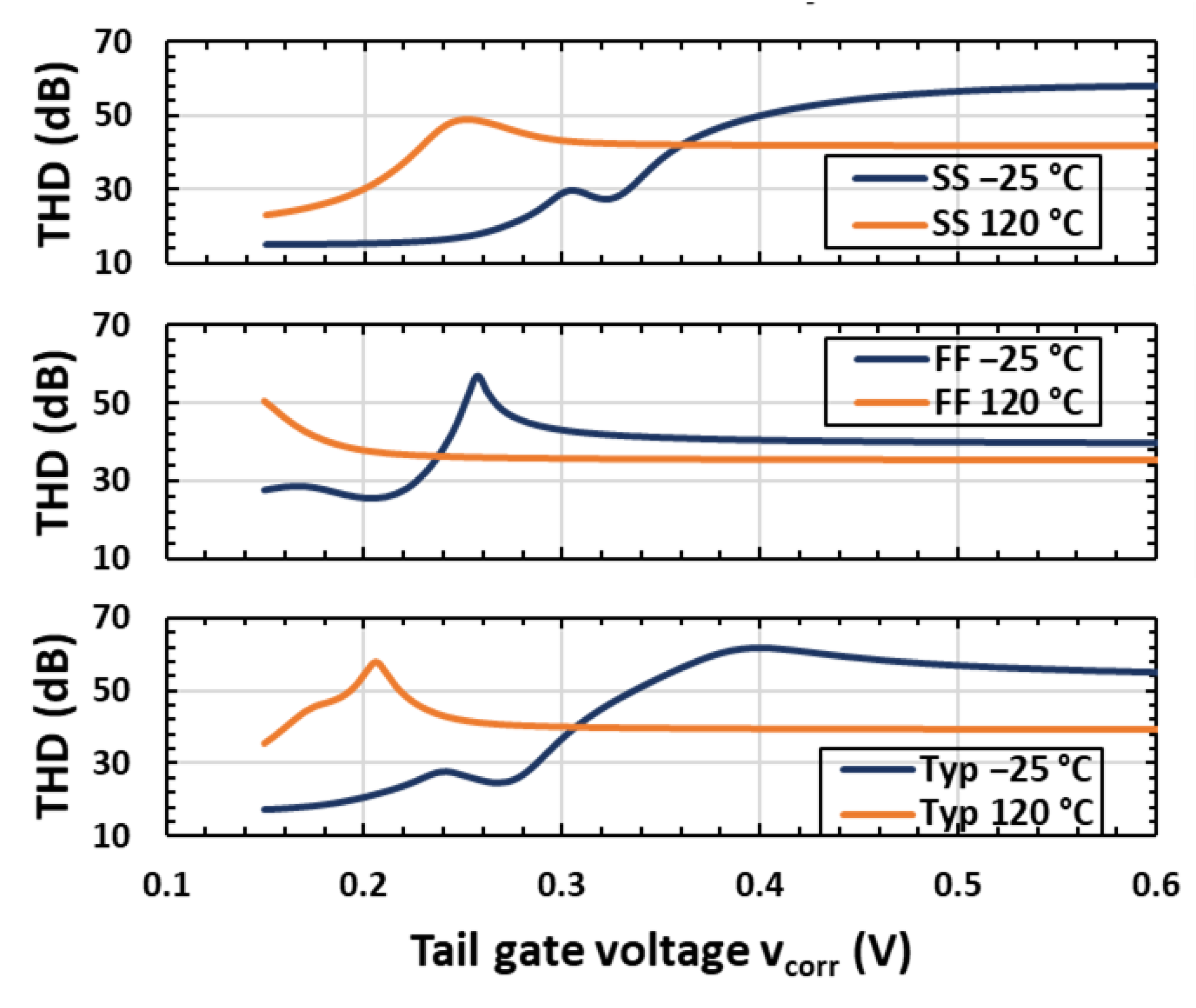
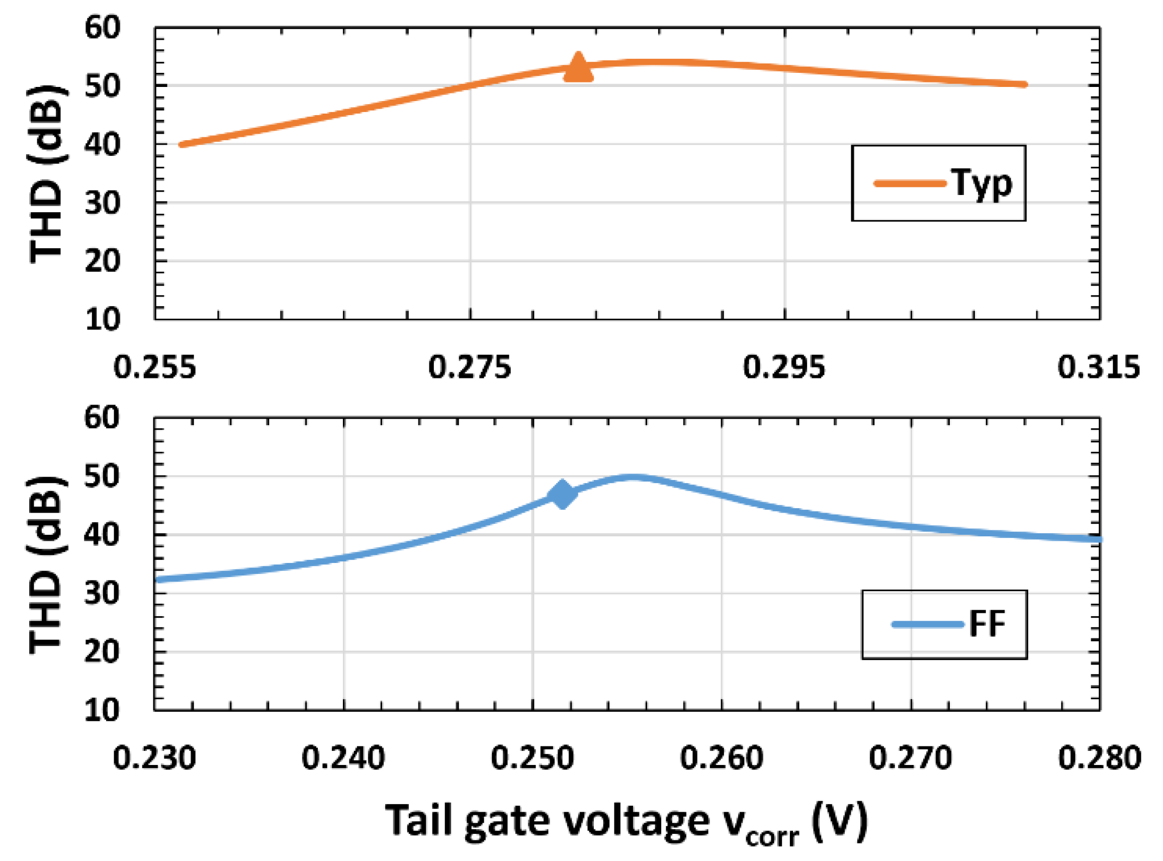
Figure 9 shows the THD of the TH output as a function of
for typical and fast process corner. The maximum linearity of over
was obtained for a value
which almost matches the one obtained through the MATLAB simulation (given the small differences between the circuit and the modeling), meaning that the calibration loop can maximize the linearity of the overall TH circuit.
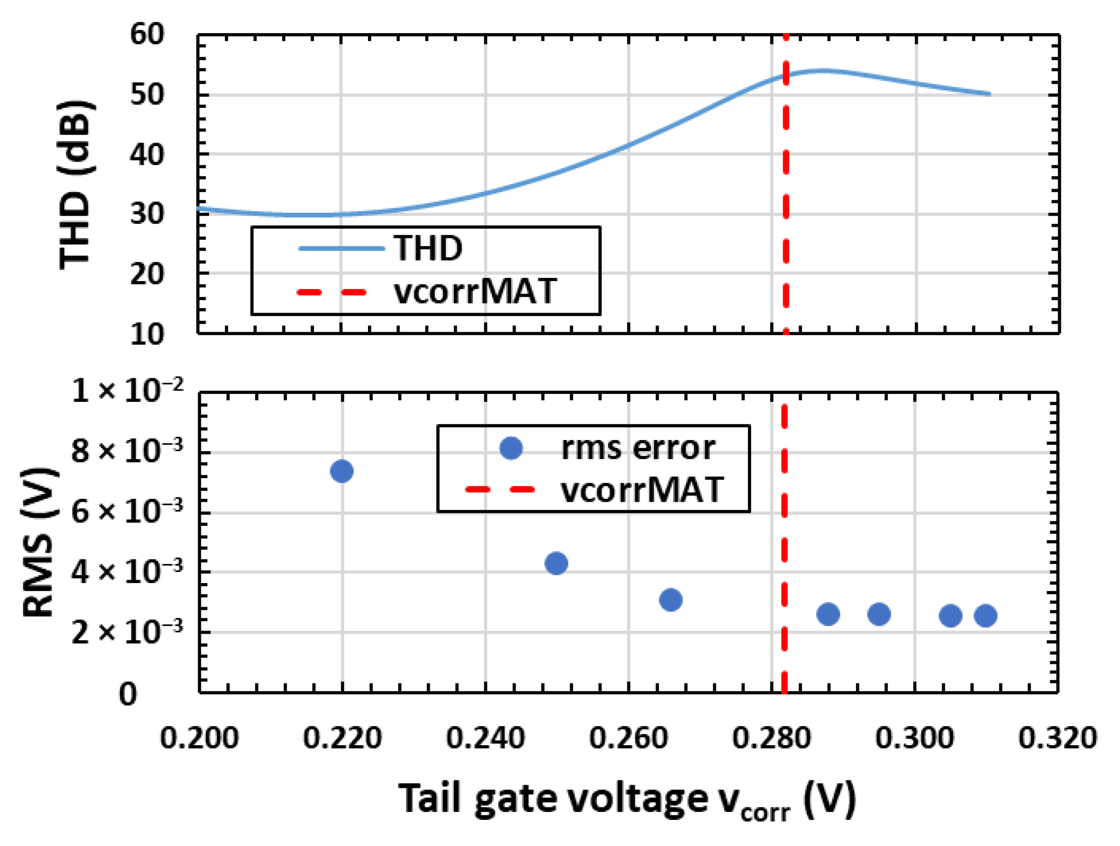
To further validate the performance improvements stemming from the proposed calibration loop, a PAM-8 Pseudo-Random Binary Stream (PRBS) input signal with a
channel attenuation at Nyquist was used. The signal was sent with two amplitudes, full scale and a tenth of the full scale, obtaining the outputs
and
. Afterwards, the following operation was performed on the output signals to verify the linearity of the circuit:
The value of the RMS error gives us an assessment of the system linearity with a PRBS input signal. In
Figure 10, we can see that the MATLAB model gives us a value of
which can almost minimize the RMS error and therefore the non-linearity, even though the model does not include the dynamic non-linearities present in the circuit simulation.
To further validate the proposed linearity calibration technique, the same MATLAB PAM-8 RX model simulation was repeated with the same TH distortion coefficients and adding an AFE with 32 dB and 36 dB THD performance. In these cases, the calibration loop converges to a
value that maximizes the overall linearity of the RX chain including the AFE. The resulting MSE at the slicer input shown in
Figure 11a shows a behavior of the calibrated systems akin to the ideal RX linearity case. The same results are visible in
Figure 11b, where the SER is very similar to the case in which the RX linearity is ideal.
5. Conclusions
This paper proposes a 8 × 8 time-interleaved TH circuit in 5 nm FinFET technology with a gain of at Nyquist and tunable non-linearities. A calibration feedback loop for a PAM-8 receiver is proposed and modeled in MATLAB, which allows maximizing the linearity of the TH. From the simulation of the MATLAB model, the voltage calibration bias of the second-stage buffer was extrapolated. Then, the bias voltage was used to perform transistor-level simulations of the analog track-and-hold buffer, obtaining a THD of over in typical process corner with a , sinusoidal input. The linearity of the system was also verified using a PAM-8 pseudorandom stream signal showing that the RMS error is indeed minimized. Lastly, the MATLAB simulation of the PAM-8 RX with a 36 dB THD AFE model shows the possibility of using this calibration technique to compensate for AFE non-linearities as well. In future works, the performances of the proposed TH circuit and calibration loop will be further verified using post-layout simulations and HDL implementation, respectively, and eventually with silicon implementation.
Author Contributions
Conceptualization, A.D.P., E.M. and N.G.; methodology, A.D.P., E.M., N.G. and C.N.; validation, A.D.P., E.M., N.G. and C.N.; formal analysis, A.D.P., E.M., N.G. and C.N.; investigation, A.D.P., E.M. and N.G.; data curation, A.D.P.; writing—original draft preparation, A.D.P.; writing—review and editing, A.D.P., E.M., N.G., C.N. and L.F.; supervision, C.N. and L.F. All authors have read and agreed to the published version of the manuscript.
Funding
This research received no external funding.
Conflicts of Interest
The authors declare no conflict of interest.
References
- Bailey, J.; Shakiba, H.; Nir, E.; Marderfeld, G.; Krotnev, P.; LaCroix, M.-A.; Cassan, D.; Tonietto, D. A 112-Gb/s PAM-4 Low-Power Nine-Tap Sliding-Block DFE in a 7-nm FinFET Wireline Receiver. IEEE J. Solid-State Circuits 2021, 57, 32–43. [Google Scholar] [CrossRef]
- Krupnik, Y.; Perelman, Y.; Levin, I.; Sanhedrai, Y.; Eitan, R.; Khairi, A.; Landau, Y.; Virobnik, U.; Dolev, N.; Meisler, A.; et al. 112 Gb/s PAM4 ADC Based SERDES Receiver for Long-Reach Channels in 10nm Process. In Proceedings of the 2019 Symposium on VLSI Circuits, Kyoto, Japan, 9–14 June 2019. [Google Scholar] [CrossRef]
- Pisati, M.; Minuti, A.; Bollati, G.; Giunco, F.; Massolini, R.G.; Cesura, G.; De Bernardinis, F.; Pascale, P.; Nani, C.; Ghittori, N.; et al. A 243-mW 1.25–56-Gb/s Continuous Range PAM-4 42.5-dB IL ADC/DAC-Based Transceiver in 7-nm FinFET. IEEE J. Solid-State Circuits 2019, 55, 6–18. [Google Scholar] [CrossRef]
- Foley, D.; Flynn, M. A low-power 8-PAM serial transceiver in 0.5-μm digital CMOS. IEEE J. Solid-State Circuits 2002, 37, 310–316. [Google Scholar] [CrossRef]
- Chong, E.; Musa, F.A.; Mustafa, A.N.; Gao, T.; Krotnev, P.; Soreefan, R.; Xin, Q.; Madeira, P.; Tonietto, D. A 112 Gb/s PAM-4, 168 Gb/s PAM-8 7 bit DAC-Based Transmitter in 7nm FinFET. In Proceedings of the ESSCIRC 2021—IEEE 47th European Solid State Circuits Conference (ESSCIRC), Grenoble, France, 13–22 September 2021; pp. 523–526. [Google Scholar] [CrossRef]
- Chun, Y.; Megahed, M.; Ramachandran, A.; Anand, T. A PAM-8 Wireline Transceiver with Linearity Improvement Technique and a Time-Domain Receiver Side FFE in 65 nm CMOS. IEEE J. Solid-State Circuits 2022, 57, 1527–1541. [Google Scholar] [CrossRef]
- Megahed, M.; Chun, Y.; Wang, Z.; Anand, T. A 27 Gb/s 5.39 pJ/bit 8-ary Modulated Wireline Transceiver Using Pulse Width and Amplitude Modulation Achieving 9.5 dB SNR Improvement over PAM-8. In Proceedings of the 2021 Symposium on VLSI Circuits, Kyoto, Japan, 13–19 June 2021. [Google Scholar] [CrossRef]
- Li, J.; Wu, S.; Liu, Y.; Ning, N.; Yu, Q. A Digital Timing Mismatch Calibration Technique in Time-Interleaved ADCs. IEEE Trans. Circuits Syst. II Express Briefs 2014, 61, 486–490. [Google Scholar] [CrossRef]
- Hung, T.-C.; Liao, F.-W.; Kuo, T.-H. A 12-Bit Time-Interleaved 400-MS/s Pipelined ADC With Split-ADC Digital Background Calibration in 4000 Conversions/Channel. IEEE Trans. Circuits Syst. II Express Briefs 2019, 66, 1810–1814. [Google Scholar] [CrossRef]
- Zhao, H.; Diaz, J.C.G.; Hoyos, S. Multi-Channel Receiver Nonlinearity Cancellation Using Channel Speculation Passing Algorithm. IEEE Trans. Circuits Syst. II Express Briefs 2021, 69, 599–603. [Google Scholar] [CrossRef]
- Bocco, A.F.; Solis, F.; Reyes, B.T.; Morero, D.A.; Hueda, M.R. Background Compensation of Static TI-ADC Nonlinearities in Coherent Optical Receivers. In Proceedings of the 2021 Argentine Conference on Electronics (CAE), Bahia Blanca, Argentina, 11–12 March 2021; pp. 45–49. [Google Scholar] [CrossRef]
- Di Pasquo, A.; Nani, C.; Monaco, E.; Fanucci, L. A High Linearity Driver with Embedded Interleaved Track-and-Hold Array for High-Speed ADC. In Proceedings of the 2021 IEEE International Symposium on Circuits and Systems (ISCAS), Daegu, Korea, 22–28 May 2021; pp. 1–5. [Google Scholar] [CrossRef]
- Mattia, O.E.; Murmann, B. 80 GS/s 5.5 ENOB time-interleaved inverter-based CMOS track-and-hold. Electron. Lett. 2020, 56, 328–329. [Google Scholar] [CrossRef]
- Zheng, K.; Frans, Y.; Ambatipudi, S.L.; Asuncion, S.; Reddy, H.T.; Chang, K.; Murmann, B. An Inverter-Based Analog Front-End for a 56-Gb/s PAM-4 Wireline Transceiver in 16-nm CMOS. IEEE Solid-State Circuits Lett. 2019, 1, 249–252. [Google Scholar] [CrossRef]
| Publisher’s Note: MDPI stays neutral with regard to jurisdictional claims in published maps and institutional affiliations. |
© 2022 by the authors. Licensee MDPI, Basel, Switzerland. This article is an open access article distributed under the terms and conditions of the Creative Commons Attribution (CC BY) license (https://creativecommons.org/licenses/by/4.0/).


