Article

Voltage Ripple Suppression Methods for the Capacitor in Modular Multilevel Converter Submodules Employing a Reversed Pulse Width Modulation-Switching Channel

College of Information Science and Technology, Donghua University, Shanghai 201620, China
*
Author to whom correspondence should be addressed.
Electronics 2022, 11(14), 2193; https://doi.org/10.3390/electronics11142193
Submission received: 21 June 2022 / Revised: 11 July 2022 / Accepted: 12 July 2022 / Published: 13 July 2022
(This article belongs to the Section Power Electronics)

Abstract

:
Modular multilevel converters (MMCs) will be widely applied in onboard integrated power systems due to their high levels of electric power output and good-quality sine waveform outputs. However, the capacitor voltage of MMCs fluctuates greatly because the charge–discharge process of the capacitor is continuous when the system is working. In order to reduce voltage ripples efficiently, a capacitor voltage ripple-suppression strategy employing a reversed PWM switching channel is proposed in this paper. For one pair of the upper and lower arm submodules, a switching channel is built. Then, the highest ripple voltage possible can be offset since the voltage fluctuation direction of the upper and the lower arm capacitors would be reversed. In addition, a clamping capacitor is added to the switching channel to further suppress the fluctuation voltage by 78%. Compared to traditional large capacitance suppression methods, only 12% capacitance is used in the proposed method. The reliability and power density of the proposed MMC both increased, and there are no additional losses compared with previous voltage ripple suppression methods. The effectiveness of the proposed voltage ripple suppression strategy is verified by simulation results.

1. Introduction

All-electric ships represent an important developmental direction for ships. Thus, onboard integrated power systems have recently become a research focus [1,2]. Faced with the characteristics of high power and medium-high voltage, multilevel converters have been widely applied in onboard integrated power systems because they do not require large filters and can provide good-quality sine waveform outputs [3,4,5]. Compared to other converters, MMCs have the advantages of having a high degree of modularity, low redundancy costs, and high efficiency; thus, it has great developmental prospects [6,7,8]. However, the capacitor voltages of MMCs fluctuate greatly since the capacitors are always charged or discharged during operation, and the voltage ripple amplitude is inversely proportional to the operating frequency of the MMC [9]. Excessive voltage fluctuations lead to power imbalances within the MMC and may even deteriorate the output waveform of the MMC. In addition, the capacitor voltages in the submodules of each arm are unequal due to the existence of the capacitor parameter difference as well as the difference of the capacitor charge rate. This is called capacitor voltage imbalance, which affects the safety and the stability of the MMC system. These defects limit the use of MMCs in onboard integrated power systems. The voltage fluctuation problem not only exists in submodule capacitors but also exists in the DC output side when the MMC is used as a rectifier, especially when operating in the renewable energy system. Normally, the DC output voltage fluctuates with the change in the input power relative to the MMC rectifier. Currently, the sliding mode control has been used for stabilizing the output DC voltage in the series microgrid system under island mode [10]. Since the outputted DC voltage fluctuation is not the main problem in the onboard MMC integrated power system, it is not discussed in this paper.
The traditional method for resolving the capacitor voltage imbalance problem is the voltage-sorting method. Recently, many novel voltage-balancing methods are proposed by scholars to improve the traditional voltage-balancing method. For reducing the switching frequency of the converter, a modified capacitor voltage-balancing method based on the control algorithm of the expert system is proposed in [11]. It modifies the traditional voltage-balancing method by retaining the previous state of the submodule. Normally, large capacitors are used to suppress the voltage ripple in an MMC. In [12], a super-capacitor-based MMC topology was proposed, and the super capacitor was added in each submodule. However, a large number of submodules are usually cascaded to achieve a high voltage level in the MMC, resulting in MMCs with expensive large capacitors. Currently, many scholars have carried out research on how to suppress voltage fluctuations in MMC capacitors. The main methods include high-frequency harmonic injection and power channel transfer.
The main idea of the high-frequency harmonic injection method is to introduce the high-frequency component into the arm voltage and arm current at the same time to suppress the low frequency fluctuations in the submodule capacitor. The method was first proposed for application in MMCs by ABB [13]. Later, many scholars put forward improvements to the method, such as changing the injected high-frequency sine wave into a sine wave in addition to a third harmonic, quasi-square wave or square wave to reduce the current stress of the device [14,15,16,17,18,19] or by introducing a d-q synchronous rotation coordinate system to complete the injection method [20]. In [19], the third-order harmonic voltage and second-order harmonic current are injected in the MMC to reduce capacitor voltage ripples. In this method, the injection of the common-mode voltage is not required in the circuit of the AC side. Thus, the amplitude of the injected second-order harmonic current could be reduced, which could decrease the current stress of the injected harmonic current. However, the current stress caused by these high-frequency harmonic injection methods is still large and will increase additional losses, especially at high frequency levels [21]. The model predictive control method has been proposed by scholars for reducing the amount of calculations [22]. However, this method will also increase additional losses when the fluctuations of the capacitor voltages become large. The main reason is that, in this situation, it exhibits a similar operating pattern with the high-frequency harmonic injection method for reducing capacitor voltage ripples. Therefore, we propose a capacitor voltage-suppression method that is realized by a power channel. Here, the power channel is built between the submodules to form a path to exchange electric power [23,24,25,26]. Since the voltage fluctuation directions of the capacitors in the upper and lower arms are reversed, the power channel can be used to offset the ripple voltage. This approach experiences no current stress or additional losses but increases the number of devices. Depending on the control method, a power channel can be added between the upper and lower arms in each phase [23,24] or between the three phases [25,26]. However, these capacitor voltage ripple suppression methods have to use a DC–DC converter and a high-frequency transformer to construct the power channel to connect the submodules, which is not only complicated to control but is also more expensive. In [27], another arm, which is the same as the original arm, is added between upper and lower arms as a physical power transfer channel in each phase. Then, a cross-connected topology is constituted. This method does not require additional DC–DC converters and transformers, but the control algorithm of the power devices on the added arms is complex. In [28], the added arm in the topology of [27] was replaced by a capacitor. The circuit is simpler and costs decreased. However, it requires high frequency common-mode voltage injection and circulating current injections when in operation, which could produce additional losses.
In this paper, a novel capacitor voltage ripple suppression method employing the reversed-PWM switching channel is proposed. The capacitor voltage fluctuations of the submodules in the upper and the lower arms are analyzed. Then, a switching channel is constructed between the upper and lower submodules to form a path through which the charge in the capacitors with the potential difference can flow freely. Additionally, a clamping capacitor is added to the switching channel to further suppress the voltage ripple. Capacitors can be also used to compensate for reactive power and for introducing load balance. In [29], capacitors are used as the negative- and zero-sequence compensator topology for three-phase unbalanced loads in the distribution networks. The capacitor connection modes are controlled to switch between phase-to-phase and phase-to-ground by using intelligent grouping compound switches. Compared to traditional voltage ripple suppression strategies, the circuit topology used in this novel method is simple, and the costs are low due the removal of the DC–DC converter and the high-frequency transformer. In addition, compared with previous voltage ripple suppression methods, there are no additional losses in the proposed novel MMC. With the proposed voltage ripple suppression method, the voltage ripples of the submodule capacitors are greatly reduced. In addition, the reliability and power density of the proposed MMC also increased. The remainder of this article is organized as follows: In Section 2, the voltage ripples of the capacitors in the upper and the lower arms are analyzed. In Section 3, the submodule topologies employing the reversed PWM-switching channel are provided. The realization of this novel capacitor voltage ripple suppression method is described in Section 4. Additionally, the simulation results regarding capacitor voltage fluctuation suppression are shown in Section 5. Finally, the conclusion is provided in Section 6.

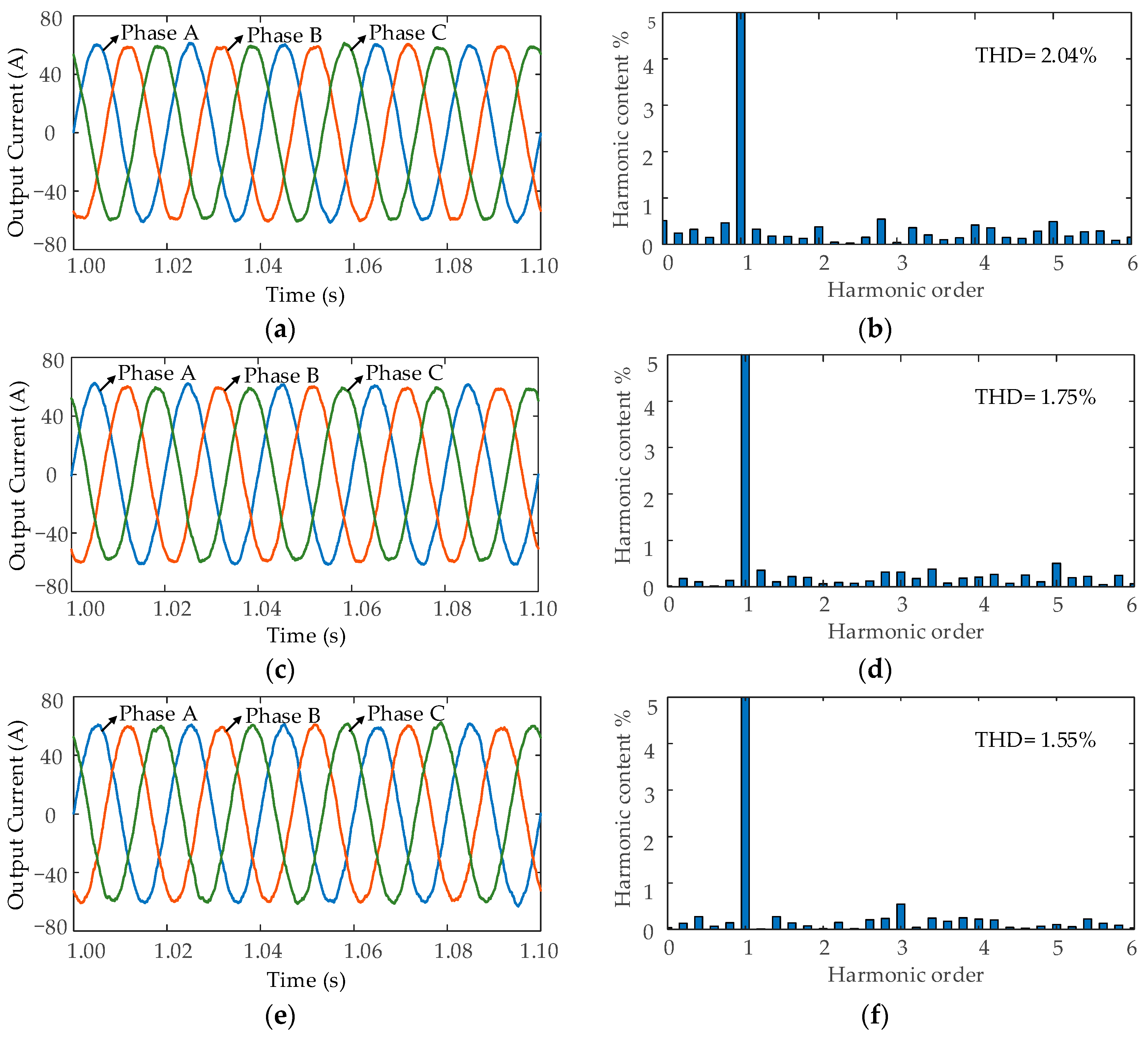
2. Analysis of the Capacitor Voltage Ripple

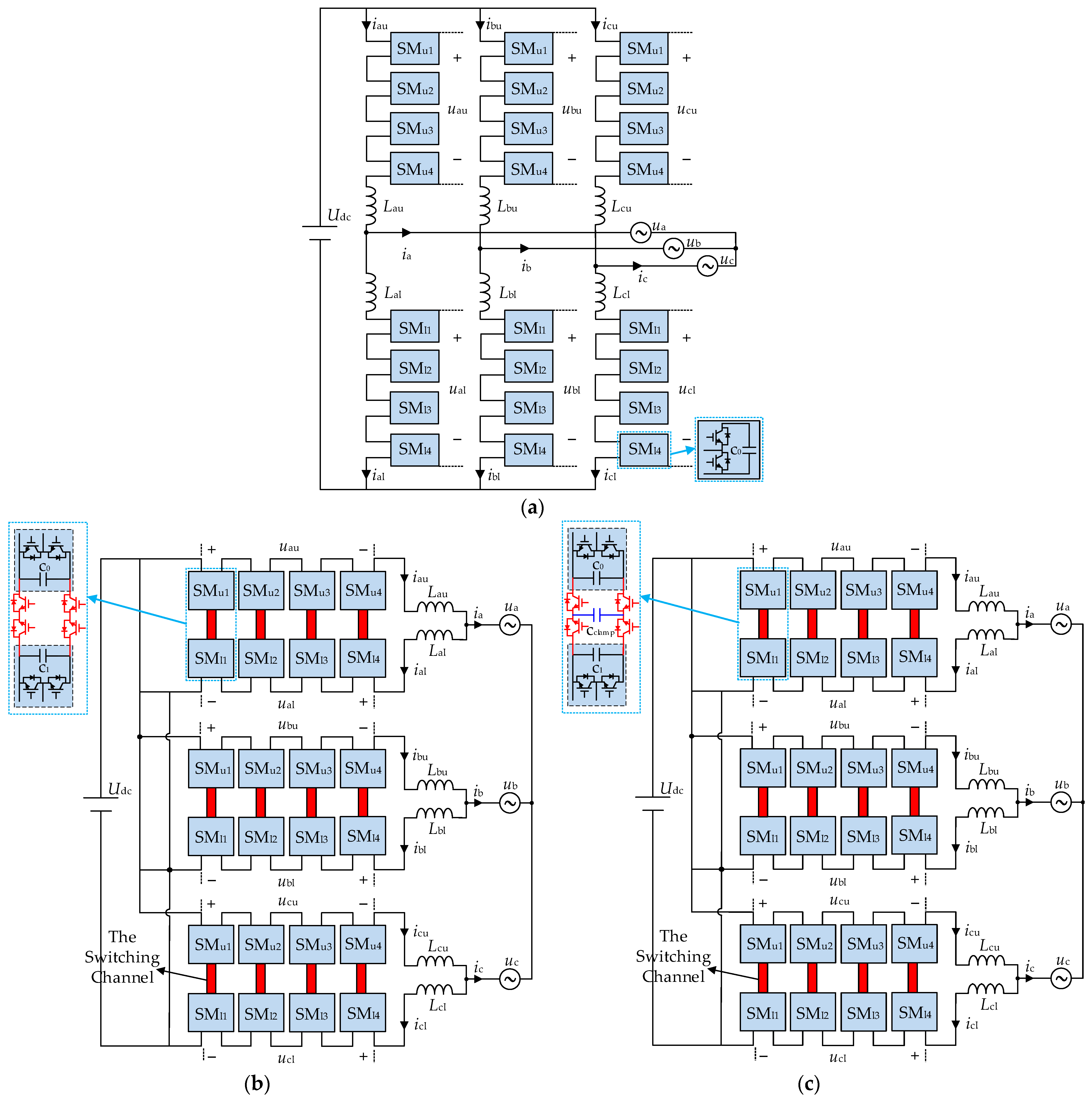
The typical topology of the MMC is shown in Figure 1a. An MMC has three phases, and each phase is divided into an upper arm and a lower arm. Each arm consists of a number of submodules and an arm inductor in series. The arm’s inductance can restrain the circulating current.
Figure 1b shows the topology of the half-bridge submodule, which is the most commonly used submodule. The submodule has three operating modes: an input mode, bypass mode, and removal mode. In Figure 1b, T1 and T2 are IGBTs, and D1 and D2 are antiparallel diodes. When T1 and T2 are switched off at the same time, the submodule is cut off; i.e., it is in a hot standby state. When T1 is switched off and T2 is switched on, the operating state of the submodule is called the bypass state. When T1 is switched on and T2 is switched off, the submodule begins its operation. In this state, the capacitor of the submodule is connected in series with the capacitors of the other submodules in operation. The sum of the series capacitor voltages is the arm voltage. The difference-mode component of the arm voltages of the upper and lower arms is the AC voltage output of each phase. It can be seen from the MMC topology that the sum of the capacitor voltages of the input submodules in each phase is equal to the DC voltage. The numbers of the input submodules of the upper and lower arms of each phase vary with time, but their sum is constant, and it is equal to the number of the submodules used in each arm.
The output voltage of each phase in the MMC is expressed as follows:
u x = M U dc 2 sin ( ω t + θ x ) = U x sin ( ω t + θ x )
where M is the voltage modulation ratio, Udc is the DC voltage, Ux is the AC voltage amplitude, and θ x is the AC voltage phase angle [28].
The output current of each phase is expressed as follows:
i x = I x sin ( ω t + θ x φ )
where Ix is the amplitude of the AC current, and φ is the load impedance angle [28].
The instantaneous output power of each phase is as follows.
p x = u x i x
Combining (1) and (2) into (3) obtains the following.
{ p a = M U dc I x 4 cos φ M U dc I x 4 cos ( 2 ω t + 2 θ x φ ) p b = M U dc I x 4 cos φ M U dc I x 4 cos ( 2 ω t + 2 θ x φ + 2 3 π ) p c = M U dc I x 4 cos φ M U dc I x 4 cos ( 2 ω t + 2 θ x φ 2 3 π )
It can be seen from (4) that the power of each phase of the MMC includes a DC component and secondary negative sequence component. The DC component is the active part of the output power, and the secondary component is stored in the capacitors of the submodules or in the DC side of the MMC.
The arm voltage of the MMC is usually controlled as follows:
{ u x u = 1 2 U d c u x = 1 2 U d c [ 1 M sin ( ω t + θ x ) ] u x l = 1 2 U d c + u x = 1 2 U d c [ 1 + M sin ( ω t + θ x ) ]
where uxu is the upper arm voltage, and uxl is the lower arm voltage of the x phase (x = a, b, c).
The output current can also be expressed as follows:
i x = i xu i xl
where ixu and ixl are the upper arm current and lower arm current of the x phase (x = a, b, c), respectively.
Define the common-mode component of the upper and lower arm currents as the circulating current ixc.
i xc = 1 2 ( i xu + i xl )
According to (6) and (7), the arm current can be expressed as follows.
{ i xu = i xc + 1 2 i x i xl = i xc 1 2 i x
The power of the upper arm and the lower arm in each phase is expressed as follows.
{ p xu = u xu i xu p xl = u xl i xl
Combining (1), (2), (5), and (8) into (9) obtains the following.
{ p xu = U dc 2 i xc + U dc I x 4 sin ( ω t + θ x φ ) M U dc 2 i xc sin ( ω t + θ x ) M U dc I x 4 sin ( ω t + θ x ) sin ( ω t + θ x φ ) p xl = U dc 2 i xc U dc I x 4 sin ( ω t + θ x φ ) + M U dc 2 i xc sin ( ω t + θ x ) M U dc I x 4 sin ( ω t + θ x ) sin ( ω t + θ x φ )
The first and the fourth terms of pxu are in phase with pxl in (10), and the second and the third terms are reversed with pxl. Since circulating current ixc mainly contains the DC component and the secondary component, the fundamental ripple of the upper and lower arm power is inverse, and the double-frequency ripple is in phase. The power ripple leads to the voltage ripple of the capacitor. Since the fundamental frequency component occupies the largest proportion in the arm power, the capacitor voltages of the upper and lower arms fluctuate inversely at the fundamental frequency.
The further analysis of (10) shows that the fluctuation amplitude is proportional to the output current amplitude and is inversely proportional to the output frequency. The large voltage fluctuation of the capacitor will challenge the withstanding voltage capability of the capacitors and the power switching devices, and it will aggravate the power imbalance inside the MMC and even deteriorate the output waveform. In order to reduce the capacitor voltage ripple of the submodule without using large-size capacitors, a new submodule topology employing a switching channel is proposed in this paper. The switching channel is constructed between the submodules of the upper and lower arms. Since the channel forms a path for charge to flow freely, it can realize the self-charge and self-discharge between the capacitors of the submodules at both sides of the channel. Thus, voltage fluctuations can be greatly reduced.

3. Submodule Topologies Employing the Reversed-PWM Switching Channel

According to the above analysis, the capacitor voltages of the submodules in the upper and lower arms demonstrate inverse fluctuations at the fundamental frequency, which will lead to periodic potential differences. If the switching channel is built between the submodules at the same position of the upper and lower arms, the charge of the capacitor with higher voltage in the upper (lower) arm can flow to a capacitor with lower voltage in the lower (upper) arm. Then, the self-charging (discharging) ability of the capacitors between the upper and lower arms can be realized. This decreases the capacitor’s voltage when it is higher than the reference voltage and increases the capacitor’s voltage when it is lower than the reference voltage. The voltages of both capacitors become close to the reference value at the same time, which means that capacitor voltage fluctuation suppression is realized.
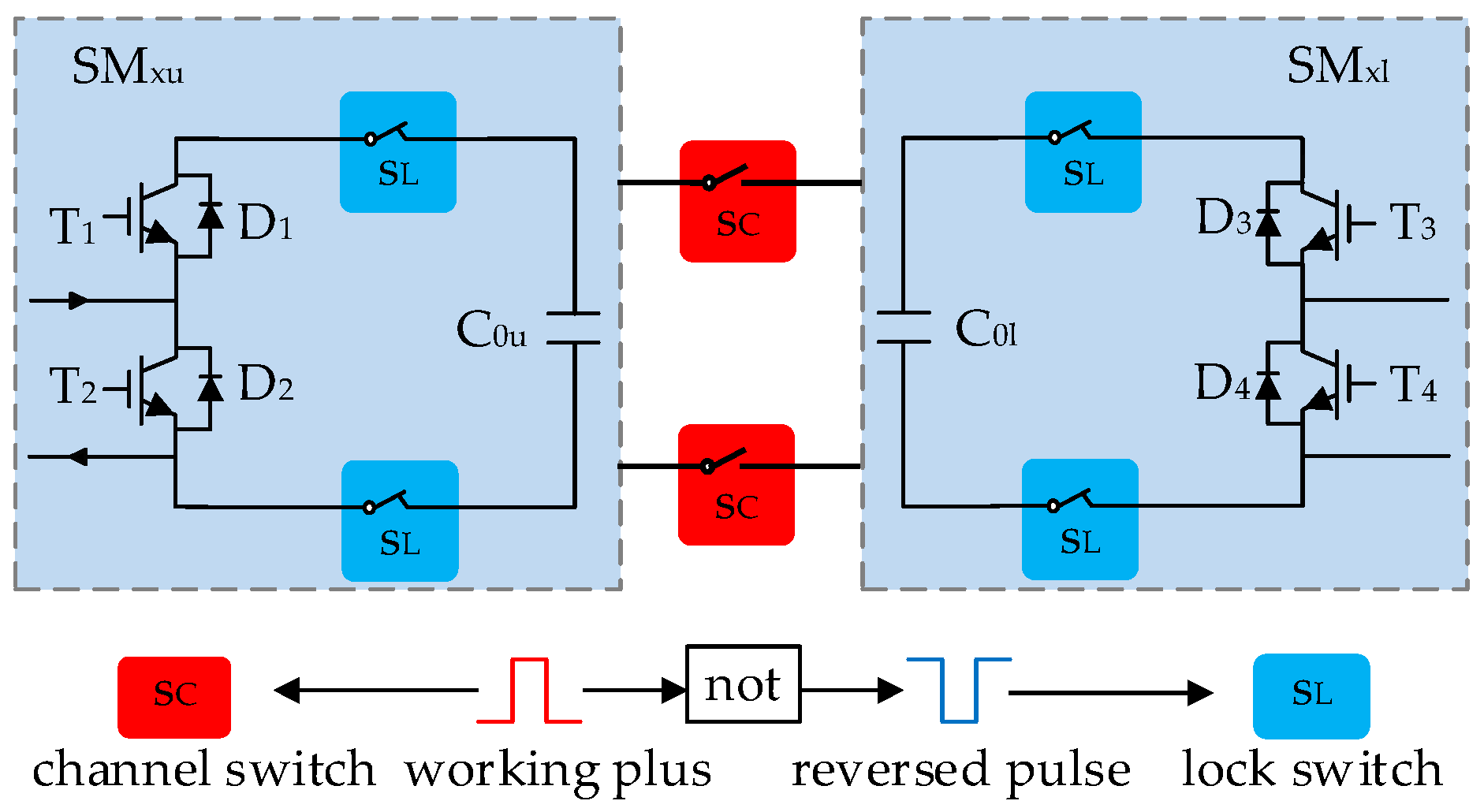
Figure 2a is the schematic diagram of the switching channel between the arms. On the left is the submodule of the upper arm, and on the right is the submodule of the lower arm. The channel between the two submodules provides a path for the charge to flow freely between the capacitors.
Because of the additional physical connection between the upper and lower arms, MMC will not work properly if the switching channel is not controlled. Moreover, we want the channel to be simple and effective, and the best method to achieve this is to limit the additional control costs added to the MMC system. In this manner, the proposed switching channel only uses the switching device to control the charge’s flow. Only when the submodules at both sides are in the bypass state at the same time does the channel input switch, and it is kept off at other times to ensure the normal operation of the MMC.
In addition, a clamping capacitor is added in the channel to further limit the voltage fluctuations to a smaller range. The submodule topology employing the switching channel with the clamping capacitor is shown in Figure 2c. The MMC topology based on the proposed submodule is shown in Figure 3.

4. Realization of the Capacitor Voltage Ripple Suppression Method with the Switching Channel

In order to realize the proposed capacitor voltage fluctuation suppression strategy, the control method and operating principle of the channel switches are both described in detail. The clamping capacitor is added in the channel for stabilizing the submodule capacitor voltage. In addition, for reducing the number of the switch devices used in the switching channel, the same position connection method and the symmetrical connection method are both provided and discussed.

4.1. Control of the Channel Switches

Since the proposed switching channel is connected to the upper and lower arms in the same phase, a new path is added to the original topology of the MMC. In order to ensure the normal operation of the MMC employing the switching channel, the on–off modes of the channel require additional control. The on–off logic of the switching channel is shown in Table 1. Only when the submodules at both ends of the channel are in bypass state will the channel be switched on. During this period, the capacitor of the submodule has no arm current flowed through and is connected to the other capacitor of the submodule at the end of the channel in parallel for charging or discharging.
Since the turn-off signal of the switching channel is obtained by the NAND logic calculation of the trigger pulses of the submodule switch devices, when the switching channel is about to be switched off, the channel will not receive the turn-off signal until the two terminal submodules of the channel are put into operation. During this period, the submodule and the switching channel are put into operation at the same time, which leads to the abnormal operation of the MMC.
In order to solve the above-mentioned timing problem, one idea is to add a dead zone before the switches in the channel are switched off. Then, we can ensure that the channel is switched off during the period after the submodule is put into operation to prevent the simultaneous operation of the submodule and the channel. However, since the input and bypass of the submodule are controlled by the capacitor voltage balance control system, predicting the bypass time of the channel in advance is difficult, so the added dead time cannot be estimated. To perform this, the dead time can be added at the end of each channel switch’s switching cycle, as shown in Figure 4. However, this method will increase the switching loss in the switches used in the channel.
In order to ensure the high efficiency and low loss of the switching channel, interlocking switches are added into the submodules to solve the above timing problem. As shown in Figure 5, Sc is the switch used in the channel, and SL is the interlocking switch. Trigger pulses of the SL and Sc are kept opposite to one another at all times. It is ensured at the hardware level that the submodules and the channel will not be put into operation at the same time. In this manner, the frequency of the channel switch is not too high, and there are no increases in switching loss.

4.2. Operating Principle of the Switching Channel

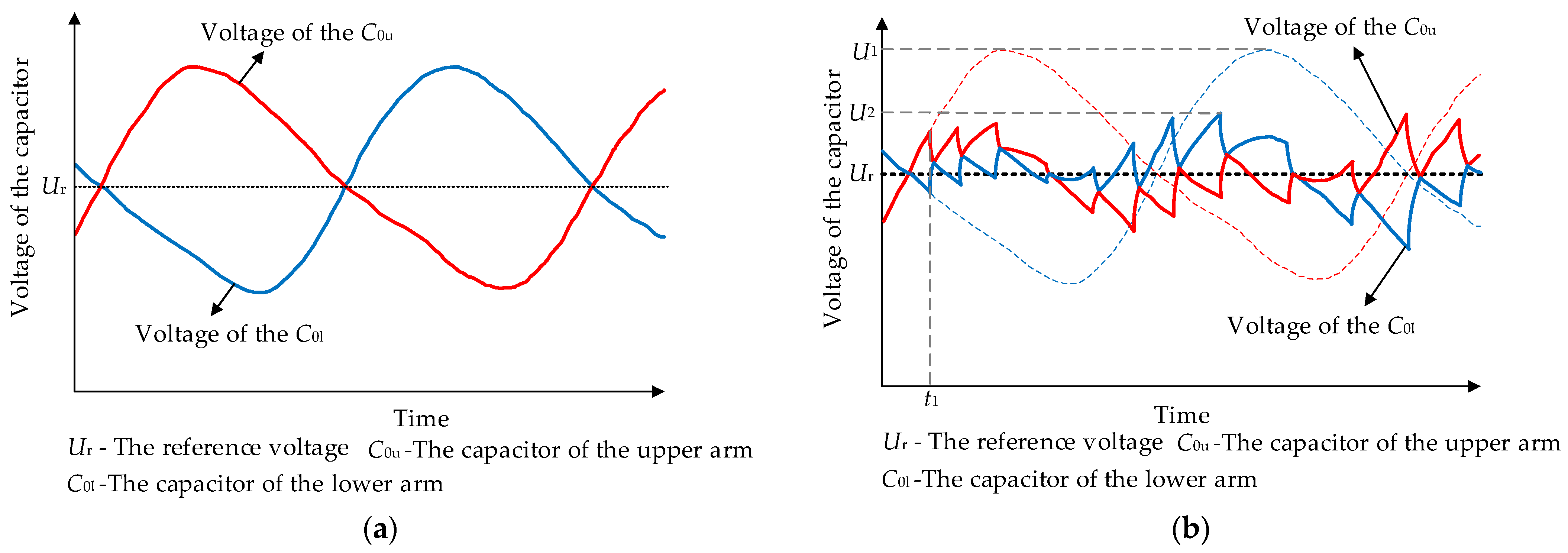
It can be seen from Formula (10) that the submodules of the upper and lower arms contain fluctuating power in the opposite direction at the fundamental frequency. The capacitor voltage fluctuations in the traditional submodules during the operation are shown in Figure 6a. It can be seen in the figure that periodic reverse ripples above and below the reference voltage value can be observed in the capacitor voltages. The voltage fluctuation could result in a periodic potential difference in the capacitors of the upper and lower arms, respectively. If the switching channel is built between the capacitors in the upper and lower arms, the capacitor with the higher voltage will charge the capacitor with lower voltage. Then, both voltages will approach the reference value at the same time, and the voltage fluctuation suppression effect is achieved.
The capacitive voltage ripples employing the switching channel are shown in Figure 6b, in which the maximum value of the voltage fluctuation is suppressed from U1 to U2. At time t1, both terminal submodules of the channel are bypassed at the same time, and the switching channel is introduced. A path is formed between the capacitors of the two submodules. Since the potential of the C0u is higher than that of C0l, the charge flows from C0u to C0l. Then, C0l voltage increases, and C0u voltage decreases until the two capacitor potentials are equal.
Since the voltage of capacitor cannot be changed suddenly, it takes time for the two capacitors to reach the same voltage. We call this period of time Δt, which is affected by the capacitance time’ constant. Additionally, we could call each duration in which the channel is in the input state time tc, which is determined by the capacitor’s voltage-balance control system. This means that tc is the duration of both the submodules at the two sides of the channel in the bypass state.
In Table 2, NSMxu and NSMxl are the number of the submodules in the input state of the upper arm and the lower arm, respectively. Ts is the duration of this stage, and T is the MMC working cycle. Additionally, P is the probability of the two-terminal modules of the channel, and it is in the bypass state at the same time. The product of Ts and P is the operating time tc of the channel at this stage. According to Table 2, the minimum non-zero value of tc is described as follows.
t cmin = ( n 1 ) T n 2 ( n + 1 )
To ensure that the energy channel works as expected, tcmin > Δt should be ensured.

4.3. Voltage Stabilizing Effect of the Clamping Capacitor

It can be obtained from the capacitor characteristics that, when the capacitance is constant, the voltage increase in the capacitor is proportional to the increase in the charge [30], which can be represented as follows.
Δ u = Δ Q C
From (12), we know that when the amount of transferred charge in the switching channel remains unchanged, an additional capacitor can be placed in the switching channel in order to further reduce fluctuations in the capacitor voltage. In addition, the added capacitor can also further clamp the capacitor’s voltage to the reference voltage UC0.

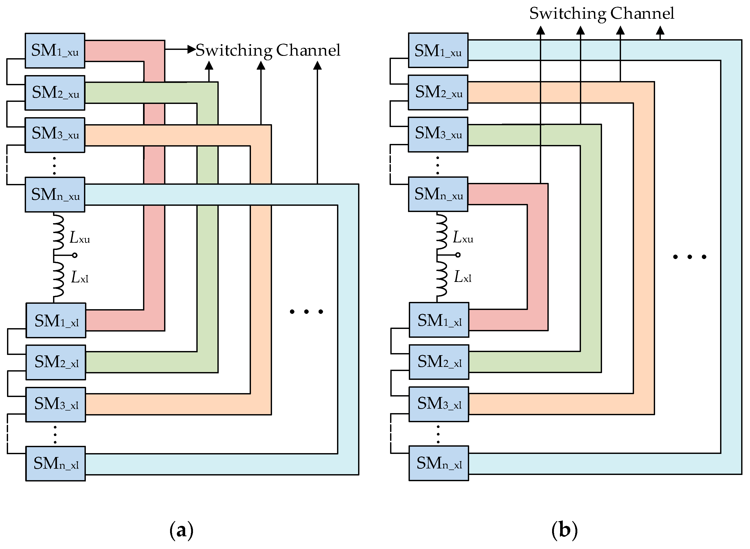
4.4. Connection Method of the Switching Channel

The switching channel is in parallel with several cascaded submodules. When the switching channel is in the off state, the voltage resulting from the channel switches is the sum of the capacitor voltages of the input submodules in parallel with it.
If the switching channel is connected with the submodules at the same position, as shown in Figure 7a, then the maximum voltage borne by each channel is nUC, i.e., DC voltage Udc. MMC is usually used in medium- and high-voltage systems; thus, Udc is generally large. It is necessary to connect multiple switch devices in the channel in series so that they can share the voltage and adopt the corresponding device voltage equalization technology.
To reduce costs, thyristors can be used in series as pressure-containing devices. The charge can only flow in one direction in the thyristor, but the switching channel requires two-way movements of the charge; thus, the thyristors in the channel need to be doubled and used in reverse parallel orientations. At the same time, since thyristors are semi-controllable devices, there must be at least two reversed IGBTs or other fully controlled devices in series in the channel to realize the full control of the input and the removal of the channel.
It is worth noting that the number of the voltage-withstanding devices used for different channel connections varies. When the same-position connection mode shown in Figure 7a is used, the maximum voltage resulting from each channel is nUC. Assuming that the withstanding voltage value of each withstanding voltage device is UT and considering a margin of 1.5 times, the total number of withstanding voltage devices required for n channels is described as follows.
K = 3 n 2 U C U T
If the channel connection mode is changed to the symmetrical connection, as shown in Figure 7b, the maximum withstanding voltage varies from 2UC to nUC due to the different numbers of submodules in parallel with each channel, and the number of withstanding voltage devices required for this connection mode is described as follows.
K = 2.25 n 2 U C U T + 1.5 n U C U T
Compared to the same-position connection mode, the symmetric connection mode reduces the number of used devices by the following.
m = ( 0.75 n 2 1.5 n ) U C U T
The proportion of the saved devices is ( 25 50 n ) % . Thus, it can be concluded from Formula (15) that when more submodules are used in the MMC with the symmetrical connection mode, the proportion of the saved devices becomes larger.

5. Simulation Results

In order to verify the effectiveness of the proposed voltage ripple suppression strategy, MMC models based on the traditional submodule and submodules employing a switching channel without a clamping capacitor and with a clamping capacitor were built in MATLAB/Simulink according to Figure 8. The MMC in the simulation is used as an inverter, and the DC side is the power supply. A phase-disposition pulse width modulation strategy is adopted. The voltage-balancing strategy used in this simulation comprises the traditional voltage-sorting method. When the arm current is positive, the submodules with the lowest capacitor voltages are put into operation and then the corresponding submodule capacitors charge, while the submodules with the highest voltage are put into operation and the corresponding submodule capacitors discharge when the arm current is negative. The system parameters of the three models are consistent and shown in Table 3.

5.1. Suppression Results of the Capacitor Voltage Ripple

Figure 9 shows the capacitor voltages of the submodules with three different topologies. Figure 9a shows the capacitor voltages of the traditional submodules. We can observe from Figure 9a that the capacitor voltages demonstrate periodic fluctuations at the frequency of 50 Hz, and the capacitor voltages of the upper arm and the lower arm fluctuate in the reversed direction. Additionally, the waveforms of the capacitor voltages of the upper and the lower arms are approximately symmetrical with respect to the reference voltage value (UC0 = 300 V). The waveform of the capacitor voltage is consistent with that of the theoretical analysis in Section 2. The peak-to-peak value of the voltage fluctuation is about 121.6 V, as seen in Figure 9a.
Figure 9b shows the capacitor voltages of the submodules employing a switching channel without a clamping capacitor. Since the switching channel provides a physical path for the charge flow between the capacitors of the upper and lower arms, the voltage fluctuations are suppressed. The peak-to-peak value of the capacitor voltage of the submodule employing the switching channel without the clamping capacitor is 56.7 V, which is 53.37% lower than that of the traditional submodule. It can also be seen from Figure 8b that the ripple directions of the capacitor voltages of the upper and lower arms is the same, which is due to the in-phase component of the upper and lower arm power.
Figure 9c shows the capacitor voltages employing the switching channel with the clamping capacitor. Additionally, the peak-to-peak voltage value of the submodule employing the switching channel with the clamping capacitor is only 25.8 V, which is 78.78% lower than that of the traditional submodule and 54.50% lower than that of the submodule employing a switching channel without a clamping capacitor. It can be seen from the capacitor voltage suppression results of the three different topologies that the proposed voltage ripple suppression strategy performs well. Thus, in the case of a same level output voltage, the submodule capacitance of the MMC with the proposed method can be reduced greatly compared to that of the MMC without a voltage ripple suppression strategy.

5.2. The Effect of the Clamping Capacitor

Figure 10 shows the details of the capacitor voltages of the submodules employing a switching channel during the charging and discharging process. It can be seen that there are many burrs on the capacitor’s voltage waveforms, which is the key to suppressing voltage fluctuations. Burrs can be divided into two parts: one part deviating from the reference voltage value (UC0 = 300 V), and the other part approaching to the reference voltage value. When the submodule is put into operation, an arm current flows through the capacitor, and the capacitor is charged (or discharged) away from the reference voltage. When the switching channel is put into operation, the capacitor is charged or discharged by another capacitor of the submodule connected with the channel because of the potential difference between the two capacitors, and the voltages of the two capacitors become close to the reference value.
It can be seen from Formula (10) that the power of the upper and lower arms has an inverted fundamental component and an in-phase secondary component. The secondary component of the power will cause in-phase voltage fluctuations in the capacitors, and this fluctuation cannot be offset by the switching channel. Therefore, the voltages as a whole exhibit in-phase fluctuations with a double fundamental frequency in Figure 10a. In Figure 10b, the capacitor’s voltage fluctuations are suppressed compared to those in the submodules employing a switching channel without a clamping capacitor. This is because the clamping capacitor increases the total capacitance in the charging path while the quantity of the electric charge required to flow through the path is the same.

5.3. Analysis of the Output AC Currents

Figure 11 shows the output AC currents of the MMC with three different topologies. Figure 11a,c,e show the waveforms of the output AC currents of the MMC with three different topologies, respectively. The THD analysis results of the phase A output currents of the aforementioned three different MMCs are shown in Figure 11b,d,f. It can be seen that the THD of the phase A output current of the conventional MMC is 2.04%, while the corresponding results of the MMCs employing the switching channels without and with a clamping capacitor are 1.75% and 1.55%, respectively. The output AC current THD of the proposed MMC employing the switching channel with a clamping capacitor decreases 24.02% compared with the traditional MMC. Thus, the waveform of the output current of the MMC employing the switching channel with the clamping capacitor has the best sine quality compared to the other two MMC topologies. This is because this kind of MMC has the smallest capacitor voltage ripple during operation.

6. Conclusions

A voltage ripple-suppression strategy employing a reversed PWM switching channel is proposed in this paper. The capacitor voltages of the submodules in the upper and lower arms are analyzed. It was found that the voltage fluctuation directions are inversed. The proposed switching channel provides a charge path between the submodules of the upper and lower arms. Then, the voltage fluctuations could be partially offset. In addition, a clamping capacitor was added to the channel’s DC bus to further suppress fluctuation voltages by approximately 78% together with the effect of the aforementioned switching channel. Therefore, the total capacitance used in the proposed method is more reduced than that of the capacitance used in the traditional capacitor voltage ripple suppression strategy. Additionally, the power density increased. Because of these advantages, the proposed switching-channel capacitor voltage-suppression method has good application prospects in onboard integrated power systems. The shortcoming of the proposed method in this paper is that only capacitor voltage-fluctuation suppression schemes under power frequency (50 Hz) situations were considered. Thus, the operating frequency of the MMC is limited. The future work will focus on widening the operating frequency of the MMC system and suppressing capacitor voltage fluctuations when the MMC is working at lower frequencies. In this case, the MMC can be used for driving high-power level motors and working in a wider range of frequencies.

Author Contributions

Conceptualization, W.Y. and F.Y.; methodology, F.Y.; software, W.Y.; validation, W.Y.; formal analysis, W.Y., F.Y. and Y.Z.; investigation, W.Y. and F.Y.; resources, F.Y.; data curation, W.Y. and F.Y.; writing—original draft preparation, W.Y.; writing—review and editing, W.Y. and F.Y.; visualization, W.Y.; supervision, F.Y.; project administration, F.Y.; funding acquisition, F.Y. All authors have read and agreed to the published version of the manuscript.

Funding

This research was funded in part by the Natural Science Foundation of Shanghai under Grant 21ZR1402300 and in part by the Fundamental Research Funds for the Central Universities under Grant 2232019D3-53.

Conflicts of Interest

The authors declare no conflict of interest.

Nomenclature

MMCModular multilevel converter
SMunThe upper arm submodule of the MMC
SMlnThe lower arm submodule of the MMC
MVoltage modulation ratio
UdcDC voltage (V)
UxThe amplitude of the AC voltage (x = a, b, c) (V)
UCCapacitor voltage (V)
UC0Reference capacitor voltage (V)
uxuUpper arm voltage of the x phase (x = a, b, c) (V)
uxlLower arm voltage of the x phase (x = a, b, c) (V)
IxThe amplitude of the AC current (x = a, b, c) (A)
ixuUpper arm current of the x phase (x = a, b, c) (A)
ixlLower arm current of the x phase (x = a, b, c) (A)
ixcCirculating current (x = a, b, c) (A)
φLoad impedance angle (rad)
θ xAC voltage phase angle of the x phase (x = a, b, c) (rad)
pxThe instantaneous output power of the x phase (x = a, b, c) (W)
pxuThe power of the upper arm of the x phase (x = a, b, c) (W)
pxlThe power of the lower arm of the x phase (x = a, b, c) (W)
TMMC working cycle (s)
TsDuration of each stage of the submodule (s)
PProbability of the two-terminal modules of the channel in the bypass state at the same time
tcDuration of the channel in the input state each time (s)
ΔtDuration of the capacitors to reach the same voltage (s)
NNumber of submodules per arm
UTThe withstanding voltage value of each withstanding voltage device (V)
KThe total number of withstanding voltage devices required

References

  1. Vicenzutti, A.; Menis, R.; Sulligoi, G. All-Electric Ship-Integrated Power Systems: Dependable Design Based on Fault Tree Analysis and Dynamic Modeling. IEEE Trans. Transp. Electrif. 2019, 5, 812–827. [Google Scholar] [CrossRef]
  2. Xu, L.; Guerrero, J.M.; Lashab, A.; Wei, B.; Bazmohammadi, N.; Vasquez, J.; Abusorrah, A.M. A Review of DC Shipboard Microgrids—Part I: Power Architectures, Energy Storage, and Power Converters. IEEE Trans. Power Electron. 2022, 37, 5155–5172. [Google Scholar] [CrossRef]
  3. Ronanki, D.; Williamson, S.S. A Simplified Space Vector Pulse Width Modulation Implementation in Modular Multilevel Converters for Electric Ship Propulsion Systems. IEEE Trans. Transp. Electrif. 2019, 5, 335–342. [Google Scholar] [CrossRef]
  4. Chen, Y.; Zhao, S.; Li, Z.; Wei, X.; Kang, Y. Modeling and Control of the Isolated DC–DC Modular Multilevel Converter for Electric Ship Medium Voltage Direct Current Power System. IEEE J. Emerg. Sel. Top. Power Electron. 2017, 5, 124–139. [Google Scholar] [CrossRef]
  5. Chen, Y.; Li, Z.; Zhao, S.; Wei, X.; Kang, Y. Design and Implementation of a Modular Multilevel Converter with Hierarchical Redundancy Ability for Electric Ship MVDC System. IEEE J. Emerg. Sel. Top. Power Electron. 2017, 5, 189–202. [Google Scholar] [CrossRef]
  6. Ronanki, D.; Williamson, S.S. Modular Multilevel Converters for Transportation Electrification: Challenges and Opportunities. IEEE Trans. Transp. Electrif. 2018, 4, 399–407. [Google Scholar] [CrossRef]
  7. Perez, M.A.; Ceballos, S.; Konstantinou, G.; Pou, J.; Aguilera, R.P. Modular Multilevel Converters: Recent Achievements and Challenges. IEEE Open J. Ind. Electron. Soc. 2021, 2, 224–239. [Google Scholar] [CrossRef]
  8. Toshon, T.A.; Faruque, M.O. Multiobjective Optimization Based Framework for Early Stage Design of Modular Multilevel Converter for All-Electric Ship Application. Energies 2022, 15, 4418. [Google Scholar] [CrossRef]
  9. Zhao, F.; Xiao, G.; Zhu, T.; Zheng, X.; Wu, Z.; Zhao, T. A Coordinated Strategy of Low-Speed and Start-Up Operation for Medium-Voltage Variable-Speed Drives with a Modular Multilevel Converter. IEEE Trans. Power Electron. 2020, 35, 709–724. [Google Scholar] [CrossRef]
  10. Xue, S.; Wang, X.; Li, X. Output Voltage Control of MMC-Based Microgrid Based on Voltage Fluctuation Compensation Sliding Mode Control. Math. Probl. Eng. 2020, 2020, 9404259. [Google Scholar] [CrossRef]
  11. Chen, Y.; Zhang, X. Voltage Balancing Method on Expert System for 51-Level MMC in High Voltage Direct Current Transmission. Math. Probl. Eng. 2016, 2016, 2968484. [Google Scholar] [CrossRef]
  12. Yang, X.; Wen, P.; Xue, Y.; Zheng, T.Q.; Wang, Y. Super Capacitor Energy Storage Based MMC for Energy Harvesting in Mine Hoist Application. Energies 2017, 10, 1428. [Google Scholar] [CrossRef] [Green Version]
  13. Korn, A.J.; Winkelnkemper, M.; Steimer, P. Low output frequency operation of the Modular Multi-Level Converter. In Proceedings of the 2010 IEEE Energy Conversion Congress and Exposition, Atlanta, GA, USA, 12–16 September 2010; pp. 3993–3997. [Google Scholar]
  14. Jung, J.-J.; Lee, H.-J.; Sul, S.-K. Control Strategy for Improved Dynamic Performance of Variable-Speed Drives with Modular Multilevel Converter. IEEE J. Emerg. Sel. Top. Power Electron. 2015, 3, 371–380. [Google Scholar] [CrossRef]
  15. Okazaki, Y.; Hagiwara, M.; Akagi, H. A Speed-Sensorless Start-Up Method of an Induction Motor Driven by a Modular Multilevel Cascade Inverter (MMCI-DSCC). IEEE Trans. Ind. Appl. 2014, 50, 2671–2680. [Google Scholar] [CrossRef]
  16. Okazaki, Y.; Kawamura, W.; Hagiwara, M.; Akagi, H.; Ishida, T.; Tsukakoshi, M.; Nakamura, R. Experimental Comparisons between Modular Multilevel DSCC Inverters and TSBC Converters for Medium-Voltage Motor Drives. IEEE Trans. Power Electron. 2017, 32, 1805–1817. [Google Scholar] [CrossRef]
  17. Debnath, S.; Qin, J.; Saeedifard, M. Control and Stability Analysis of Modular Multilevel Converter Under Low-Frequency Operation. IEEE Trans. Ind. Electron. 2015, 62, 5329–5339. [Google Scholar] [CrossRef]
  18. Kolb, J.; Kammerer, F.; Gommeringer, M.; Braun, M. Cascaded Control System of the Modular Multilevel Converter for Feeding Variable-Speed Drives. IEEE Trans. Power Electron. 2015, 30, 349–357. [Google Scholar] [CrossRef]
  19. Huang, M.; Kang, Z.; Li, W.; Zou, J.; Ma, X.; Li, J. Modified Modular Multilevel Converter with Third-Order Harmonic Voltage Injection to Reduce Submodule Capacitor Voltage Ripples. IEEE Trans. Power Electron. 2021, 36, 7074–7086. [Google Scholar] [CrossRef]
  20. Espinoza, M.; Cárdenas, R.; Díaz, M.; Clare, J.C. An Enhanced dq-Based Vector Control System for Modular Multilevel Converters Feeding Variable-Speed Drives. IEEE Trans. Ind. Electron. 2017, 64, 2620–2630. [Google Scholar] [CrossRef]
  21. Li, B.; Zhou, S.; Xu, D.; Yang, R.; Xu, D.; Buccella, C.; Cecati, C. An Improved Circulating Current Injection Method for Modular Multilevel Converters in Variable-Speed Drives. IEEE Trans. Ind. Electron. 2016, 63, 7215–7225. [Google Scholar] [CrossRef]
  22. Gao, X.; Tian, W.; Pang, Y.; Kennel, R. Model-Predictive Control for Modular Multilevel Converters Operating at Wide Frequency Range with a Novel Cost Function. IEEE Trans. Ind. Electron. 2022, 69, 5569–5580. [Google Scholar] [CrossRef]
  23. He, L.; Zhang, K.; Xiong, J.; Fan, S.; Chen, X.; Xue, Y. New modular multilevel converter with power channels between upper- and lower arms suitable for MV drives. In Proceedings of the 2015 IEEE Applied Power Electronics Conference and Exposition (APEC), Charlotte, NC, USA, 15–19 March 2015; pp. 799–805. [Google Scholar]
  24. Wang, X.; Ge, Q.; Chu, Z.; Luo, Y.; Sun, Z.; Li, Y.; Lv, X. A novel Modular Multilevel Converter topology with auxiliary voltage clamping circuit for high voltage motor drive. In Proceedings of the 2014 9th IEEE Conference on Industrial Electronics and Applications, Hangzhou, China, 9–11 June 2014; pp. 1392–1397. [Google Scholar]
  25. Du, S.; Wu, B.; Zargari, N. A Control Strategy for Star-Channel Modular Multilevel Converter in Variable-Speed Motor Drive Application. IEEE Trans. Ind. Electron. 2019, 66, 5094–5101. [Google Scholar] [CrossRef]
  26. Du, S.; Wu, B.; Zargari, N.R. A Delta-Channel Modular Multilevel Converter for Zero/Low-Fundamental-Frequency Operation. IEEE Trans. Ind. Electron. 2019, 66, 2227–2235. [Google Scholar] [CrossRef]
  27. Du, S.; Wu, B.; Tian, K.; Zargari, N.R.; Cheng, Z. An Active Cross-Connected Modular Multilevel Converter (AC-MMC) for a Medium-Voltage Motor Drive. IEEE Trans. Ind. Electron. 2016, 63, 4707–4717. [Google Scholar] [CrossRef]
  28. Le, D.D.; Lee, D.-C. Current Stress Reduction and Voltage Total Harmonic Distortion Improvement of Flying-Capacitor Modular Multilevel Converters for AC Machine Drive Applications. IEEE Trans. Ind. Electron. 2022, 69, 90–100. [Google Scholar] [CrossRef]
  29. Sun, Q.; Zhou, J.; Liu, X.; Yang, J. A Novel Load-Balancing Method and Device by Intelligent Grouping Compound Switches-Based Capacitor Banks Shunt Compensation. Math. Probl. Eng. 2013, 2013, 347361. [Google Scholar] [CrossRef]
  30. Pang, Y.; Ma, G.; Liu, X.; Xu, X.; Zhang, X. A New MMC Sub-Module Topology with DC Fault Blocking Capability and Capacitor Voltage Self-Balancing Capability. Energies 2021, 14, 3409. [Google Scholar] [CrossRef]
Figure 1. Topology of MMC: (a) three-phase MMC topology; (b) topology of a half-bridge submodule (SMn).
Electronics 11 02193 g001
Figure 2. Proposed submodule topology: (a) schematic diagram of the switching channel; (b) submodule employing the switching channel; (c) submodule employing the switching channel with the clamping capacitor.
Electronics 11 02193 g002
Figure 3. MMC topology based on new submodules.
Electronics 11 02193 g003
Figure 4. Position of the dead zone of the channel switch trigger pulse.
Electronics 11 02193 g004
Figure 5. Submodule based on interlocking switches.
Electronics 11 02193 g005
Figure 6. Schematic diagram of voltage suppression: (a) schematic diagram of capacitor voltage fluctuation without suppression method; (b) schematic diagram of capacitor voltage fluctuation with proposed suppression method.
Electronics 11 02193 g006
Figure 7. Two connection modes: (a) same position connection method; (b) symmetrical connection method.
Electronics 11 02193 g007
Figure 8. Simulation models of the MMC: (a) MMC based on the traditional submodule; (b) MMC based on the submodules employing a switching channel without a clamping capacitor; (c) MMC based on the submodules employing a switching channel with a clamping capacitor.
Electronics 11 02193 g008
Figure 9. Voltages of the submodule capacitors: (a) traditional submodule; (b) submodule employing a switching channel without the clamping capacitor; (c) submodule employing a switching channel with the clamping capacitor.
Electronics 11 02193 g009
Figure 10. The capacitor voltages of the submodules employing the switching channel during charging and discharging process: (a) the capacitor voltages of the submodules employing a switching channel without a clamping capacitor; (b) the capacitor voltages of the submodules employing a switching channel with a clamping capacitor.
Electronics 11 02193 g010
Figure 11. The output AC currents of the MMC with three different topologies: (a) the output AC current of the MMC with the traditional submodule; (b) THD of the output AC current of the MMC with traditional submodule (phase A); (c) the output AC current of the MMC employing the switching channel without a clamping capacitor; (d) THD of the output AC current of the MMC employing the switching channel without a clamping capacitor (phase A); (e) the output AC current of the MMC employing a switching channel with a clamping capacitor; (f) THD of the output AC current of the MMC employing a switching channel with a clamping capacitor (phase A).
Electronics 11 02193 g011
Table 1. Power channel control logic.
SMuSM1Power Channel
inputinputoff
inputbypassoff
bypassinputoff
bypassbypasson
Table 2. Input probability of the switching channel.
NSMxu012n
NSMxlnn − 1n − 20
Ts T n + 1 T n + 1 T n + 1 T n + 1
P0 n 1 n 1 n n 2 n 2 n 0
Table 3. Parameters of the simulation model.
SymbolParameterValue
UdcDC bus voltage1200 V
NNumber of submodules per arm4
UC0,C1Reference capacitor voltage300 V
C0,1Submodule capacitor666 μF
CclampClamping capacitor666 μF
Lau,bu,cuInductance of the upper Arm4 mH
Lal,bl,clInductance of the lower Arm4 mH
Ia,b,cRated amplitude of AC current60 A
Ua,b,cRated amplitude of AC voltage400 V
fRated frequency50 Hz
fsSwitching frequency2 kHz
Publisher’s Note: MDPI stays neutral with regard to jurisdictional claims in published maps and institutional affiliations.

