Article

A Simplified Output Feedback Controller for the DC-DC Boost Power Converter

by
Satyajit Chincholkar
1,*,
Wentao Jiang
2,
Chok-You Chan
3 and
Shriram S. Rangarajan
1,4,*
1
Department of Electrical and Electronics Engineering, SR University, Warangal 506371, India
2
School of Automation, Northwestern Polytechnical University, Xi’an 710072, China
3
School of Electrical and Electronic Engineering, Nanyang Technological University, Singapore 639798, Singapore
4
School of Electrical and Computer Engineering, Clemson University, Clemson, SC 29634, USA
*
Authors to whom correspondence should be addressed.
Electronics 2021, 10(4), 493; https://doi.org/10.3390/electronics10040493
Submission received: 25 January 2021 / Revised: 15 February 2021 / Accepted: 18 February 2021 / Published: 19 February 2021
(This article belongs to the Special Issue Multifaceted Applications of Power Electronics)

Abstract

:
Boost-type dc-dc converters present non-minimum phase dynamic system characteristics. Therefore, controller design using only the output voltage for feedback purposes is not a very straightforward task. Even though output voltage control can be achieved using inductor current control, the implementation of such current-mode controllers may require prior knowledge of the load resistance and also demand more states such as one or more currents in feedback. In this paper, the development of a new output feedback controller for boost-type dc-dc converters is presented. The controller form is such that it avoids the possibility of saturation in the control signal due to division by zero. The basic structure of the proposed controller is firstly obtained from the expression of the open-loop control signal, and the complete controller structure is then derived to satisfy the closed-loop stability conditions. Simulation and experimental results clearly verify the ability of the control law to provide robust regulation against parameter variations.

1. Introduction

Step-up dc-dc converters are used in various applications, such as energy generation using renewable resources, electric vehicles, hybrid electric vehicles, and so on [1,2,3]. However, the output voltage regulation of these converters is not a very straightforward task, as they exhibit non-minimum phase dynamic system characteristics [4]. This does not easily allow control of the output voltage using a single voltage sensor. To address this, voltage regulation is usually achieved by controlling the inductor current in the converter [4,5,6,7,8]. In ref. [5], a linear state feedback along with an integral action based on output voltage is employed to implement current-mode control. In ref. [6], it has been shown that a current-mode control scheme consisting of a proportional-current feedback and an integral voltage-feedback is sufficient to regulate the quasi-resonant converter. Moreover, a non-linear controller of the exponential form has been attempted in [7]. Even though the indirect approach of regulation discussed in refs. [5,6,7] offers several advantages, including faster transient response as well as overload protection [7]; this approach has a certain drawback: it requires the usage of a reference inductor current to realize the control law. The reference inductor current in turn is computed using the load resistance R term. In practical systems R could be unknown and also could vary. To address this, an adaptive control law [9,10,11] can be used. However, it incurs complex hardware circuitry, and it is still required to sense the inductor current, which results in extra cost and complexity due to the use of an additional current sensor.
Recently, sliding-mode control (SMC) has become a popular control methodology for regulating boost-type dc-dc converters [12,13,14,15,16,17,18,19,20,21]. The traditionally used hysteresis-modulation (HM) based SMC has many benefits, such as simplicity of realization and being less prone to saturation at large duty cycle values [14,15,16]. However, the changing switching frequency could not only cause higher switching losses in the converter but also leads to generation of electromagnetic interference (EMI) [17]. To address this, a constant-frequency SMC can be used [18]. However, such a controller adopts a single integral action in its sliding surface which is not sufficient to fully eliminate steady-state errors [19,20]. The use of an additional integral action could increase the controller’s order and its implementation complexity [18,19,20,21]. Ideally, a lower-order controller is preferred for reduced cost and simplicity. Interestingly, in most of these works related to SMC, the controller is realized based on the inductor current feedback, which results in extra hardware circuitry and cost because of the current sensor.
Recently, some passivity-based controllers were employed for boost converters [22,23]. This type of controller has simple architecture and does not need a current sensor. However, the structure of the controller proposed in [22] is such that there is a possibility of division by zero in the control signal, which could ultimately result in the saturation of the control signal. Additionally, one of the equilibrium points in the “remaining dynamics” of the closed-loop system is unstable [22].
In this paper, the development of a new output feedback controller is presented for the boost converter. Initially, the basic controller structure is given based on the expression of the open-loop transfer function, and subsequently the entire structure is obtained satisfying the stability conditions. The feasibility of the controller is shown, and tuning guiding principles are derived to obtain the smooth transient response. The main advantage of the proposed controller is that it avoids the possibility of saturation in the control signal due to division by zero as compared to that of [16]. Moreover, the closed-loop system has only one equilibrium point, which is always stable.

2. Derivation and Analysis of the Output Feedback Controller

Figure 1 shows the circuit diagram of the boost converter. The control problem of this converter is addressed in this section. The output voltage is regulated directly, despite the non-phase dynamic response of the converter.

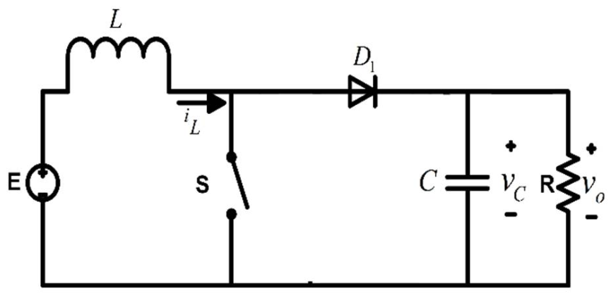
2.1. Averaged State-Space Model of the Boost Converter

The system dynamics of the boost converter are given by [4]:
d i L d t =   1 u L v c + E L
d v c d t =   1 u C i L 1 R C v c
here, i L and v C = v o   are the current through the inductor and voltage across the capacitor, respectively. The scalar u represents the control signal such that   0 < u < 1 . By equating Equations (1) and (2) to zero, the steady-state equations are obtained:
I L =   V C 2 R E ,   U = 1 E V C
where   I L , V C = V o , and U are the steady-state values of i ˙ L , v C = v o , and u , respectively. Setting V C = V d where V d is the desired voltage (with   0 < E < V d ) gives
I L =   V d 2 R E   ,   V C = V d   ,   U = V d E V d
The problem at hand is to find a suitable output feedback controller to regulate the boost converter.

2.2. Derivation of the Proposed Output Feedback Controller

Here, the derivation of the structure of the proposed controller for the step-up converter is given. To this end, the preliminary structure of the output feedback controller is firstly derived from the equation of the open-loop control law given by Equation (4), and the complete form is subsequently derived to satisfy the closed-loop stability conditions. Here x 1 = i L and x 2 = v o represent the state variables, and x 1 and x 2 represent their steady values, respectively. The form of the proposed controller can be written as
u = x 2 d   E V d
where
d x 2 d d t = f x 2 d , e 2  
In Equation (6), e 2 =   x 2 x 2 d   . Here, V d in expression of U in Equation (4) is replaced by   x 2 d , a new state variable. This results in a control law Equation (5) that is not dependent on the load resistance R of the converter. Moreover, as contrast to ref. [22], a constant reference voltage V d is used in the denominator, which avoids the problem of saturation of control signal due to division by zero. A suitable function, i.e., f x 2 d , e 2 , is needed such that the closed-loop error system is stable and in the steady-state, d x 2 d d t = 0 when x 2 d = V d and   e 2 = 0 is satisfied. The error vector is defined as follows:
e = x x d
where   e = e 1   e 2 T , x = x 1   x 2 T , and x d = x 1 d   x 2 d T . Substituting Equation (5) into Equations (1) and (2) and using Equations (6) and (7), and   x 1 d = V d 2 / R E yields
d e 1 d t =   1 L x 2 d   V d E V d e 2 + x 2 d + E L
d e 2 d t =   1 C V d     x 2 d   +   E V d e 1 + V d 2 R E 1 R C e 2 + x 2 d + f x 2 d , e 2  
d x 2 d d t =   f x 2 d , e 2  
The equilibrium point of Equations (8)–(10) can be obtained as   ( e 1 , e 2 , x 2 d ) = (   0 ,   0 ,   V d   ).Linearizing Equations (8)–(10) about this equilibrium point leads to the system of the form
d z d t =   N z
where   z = [ z 1   z 2   z 3 ] T = e 1 e 1   e 2 e 2 x 2 d x 2 d T is the state vector, and N is given by
N =   0 E L V d 1 L 1 E V d E C V d f e 2 1 R C 1 R C 1 + V d E + f x 2 d 0 f e 2 f x 2 d
here f . is evaluated at   ( e 1 , e 2 , x 2 d ) . Using Laplace transform for Equation (11) yields
s I N   =   s 3 + n 2   s 2 + n 1 s + n 0
where the coefficients of this polynomial are given by
n 2 = f x 2 d f e 2 + 1 R C , n 1 =   1 R C f x 2 d f e 2 1 + V d E + E 2 L C V d 2 , n 0 = E L C V d f e 2 1 E V d + E V d f x 2 d
The system represented by Equation (11) will be stable if all the eigenvalues of N – that is, the roots of |   s I N | = 0, where s is a complex variable–lie in the open left-half complex plane. The conditions for stability can be summarized as n i s > 0 and   n 1 n 2 n 0 > 0 , which lead to the conditions given by
f x 2 d = K 1 C > 0 ,   f e 2 = K 2 C ,   and   K 1 > K 2 V d E E
where K 1 and K 2 are positive constants. Using Equation (14), the function f x 2 d , e 2 can be written as
f x 2 d , e 2   = K 1 C x 2 d K 2 C e 2 + q
where q is a constant. Substituting (15) into (6) and using e 2 = x 2 x 2 d gives
d x 2 d d t = K 1 + K 2 C x 2 d + K 2 C x 2 q
In order satisfy the equilibrium condition given by   d x 2 d d t = 0 , when   x 2 d = V d and   e 2 = 0 , (16) can be rewritten as
d x 2 d d t = K 1 + K 2 C x 2 d + K 2 C x 2 + K 1 C V d
Equation (5), along with Equation (17), represents the complete form of the proposed output feedback controller, which is linear. As can be seen from Equations (5) and (17), the implementation this controller requires only the output voltage for feedback purposes.

2.3. Tuning Guidelines

Here, tuning guiding principles are proposed to attain the required output response. Using Equation (14) in Equations (12) and (13), the characteristic polynomial can be rewritten as
s I N   =   s 3 + n 2   s 2 + n 1 s + n 0
where
n 2 = K 1 C + K 2 C + 1 R C ;   n 1 =   K 1 R C 2 + K 2 R C 2 1 + V d E + E 2 L C V d 2 ;   n 0 = K 1 E 2 L C 2 V d 2 + K 2 E E V d L C 2 V d 2
Using Laplace transform for Equation (11) and using   z 3 0   = 0 , i.e., setting   x 2 d 0   = V d gives
z 3 s   = K 2 C   z 2 0   s + E C V d       z 1 0   z 2 0   s 3 + n 2   s 2 + n 1 s + n 0
During start up, x 1 0   =   x 2 0   = 0 , which results in,   z 1 0   = V d 2 / R E and z 2 0   = V d . Thus, (20) can be written as
z 3 s   = K 2 C   V d   s + 1 R C   s 2 + 2 ξ ω n s + ω n 2 s + p
It should be noted that the denominator of Equation (20) is rewritten as s 2 + 2 ξ ω n s + ω n 2 s + p , where ω n and ξ are the un-damped natural frequency and damping ratio of the standard second-order system z 3 s / R s   =   ω n 2 /   s 2 + 2 ξ ω n s + ω n 2 , respectively [24], and p is a positive constant. In order to achieve system behavior like the standard second-order system, the third pole must be chosen as p = 1 / R C . This results in pole-zero cancellation, and the zero 1 / R C has no effect on the output response. Comparing the denominators of Equation (20) and Equation (21) yields
    s 3 + n 2   s 2 + n 1 s + n 0 =   s 2 + 2 ξ ω n s + ω n 2 s + 1 R C
Equating the coefficient in Equation (22) and using Equation (19) leads to
2 ξ ω n = K 1 + K 2 C
2 ξ ω n R C + ω n 2 = K 1 R C 2 + K 2 R C 2 1 + V d E + E 2 L C V d 2
ω n 2 R = K 1 E 2 L C V d 2 + K 2 E E V d L C V d 2
Using Equation (23) in Equation (24) gives
K 1 + K 2 2 4 ξ 2 C 2 K 2 V d R E C 2 E 2 L C V d 2 = 0
Also using Equations (23) and (24) in Equation (25) leads to
K 2 = K 1 R E 2 L C V d 2 E 2 L C V d 2 V d R E C 2 R E E V d L C V d 2
Equations (26) and (27) can be solved simultaneously to give the required values of K 1 and K 2 for any circuit parameters.

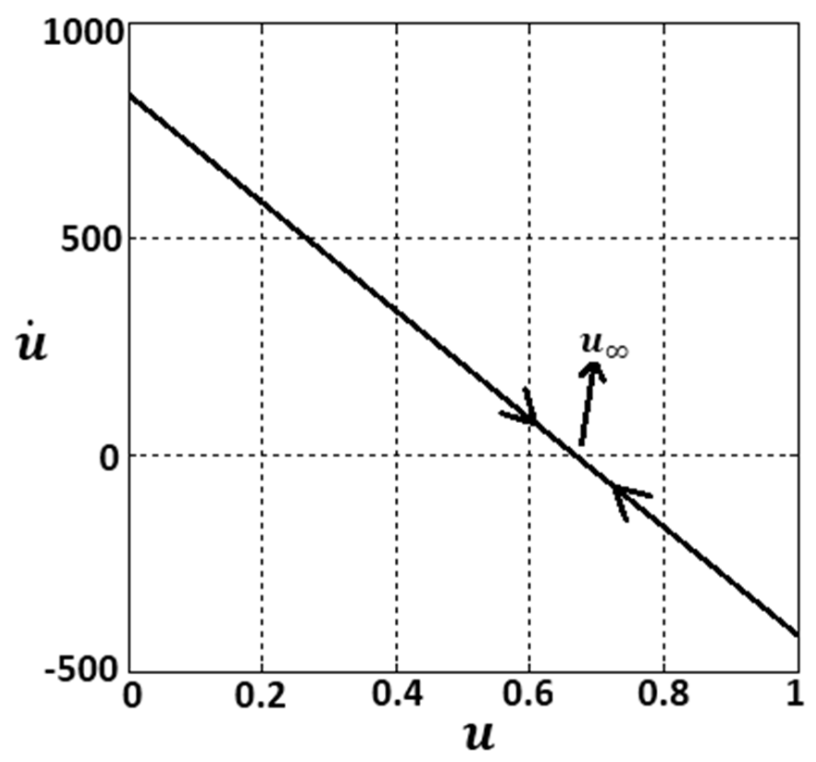
2.4. Feasibility of the Proposed Controller

The feasibility of the controller Equations (5) and (17) are now investigated. This analysis is necessary to confirm that the control input is always bounded for all operating conditions. Equation (5) gives d x 2 d d t = d u d t V d . Substituting d x 2 d d t = d u d t V d into Equation (17) and using x 2 d = u V d + E (see Equation (5)), the expression of d u d t can be obtained as
d u d t = K 1 + K 2 V d C u V d + E + K 2 V d C x 2 + K 1 C
Now, letting x 2 coincide with its desired value V d leads to
d u d t = K 1 + K 2 C u V d E V d
The phase diagram of Equation (29) using E = 5   V ,   V d = 15   V ,   C = 100   μ F , K 1 = 0.08515 , and K 2 = 0.03993 is shown in Figure 2. It is evident that u =   V d E / V d = 0.67 is the only equilibrium point in the figure.
The main result of the paper is given in the proposition.
Proposition: 
For given V d , such that   E < V d < , the control law given by Equations (5) and (17) with   K 1 > 0 ,   K 2 > 0 and     K 1 > K 2 V d E / E locally asymptotically stabilizes the boost converter to the steady-state point x 1 ,   x 2 , x 2 d   =   V d 2 / R E , V d , V d for any   0 < R < .

3. Simulation and Experimental Results

The following converter parameter values were used to validate the use of the proposed output feedback controller for the boost converter:
E = 5   V ,   V d = 15   V ,   L = 3.3   mH ,   C = 100   μ F ,   R = 220  
Substituting these parameter values into Equations (26) and (27) and using   ξ = 1 , the values of K 1 and K 2 were obtained as 0.09 and   0.04 , respectively. For implementation purposes, a voltage divider factor, β , was introduced, and Equations (5) and (17) are modified as follows:
u = x 2 d s   E s V d s
d x 2 d s d t = K 1 + K 2 C x 2 d s + K 2 C x 2 s + K 1 C V d s
where   E s = β E , V d s = β V d , x 2 s = β x 2 , x d s = β x d , and β =   1 / 10 .

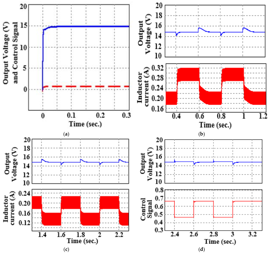
3.1. Simulation Results

Some simulations were carried out using PSIM version 9.0 to confirm the ability of the proposed controller to achieve voltage regulation in a dc-dc converter. The switching frequency used was 20 kHz.
Figure 3a indicates the transient response of the step-up converter and control signal when V d = 15   V . Output signal quickly reached the set value of the reference in ~0.03 s. Figure 3b,c shows the load change response of the system when the load was varied from R = 220   Ω   to R = 150   Ω   (vice-versa) and from R = 220   Ω   to R = 330   Ω   (vice-versa), respectively. Again, the worst-case settling time of the load-change response was obtained as ~0.04 s with a maximum overshoot of ~1 V. Figure 3d shows the converter response when input was changed from E = 5   V to E = 8   V and then back to   E = 5   V . The settling time of the response was ~0.025 s with a worst-case overshoot of ~0.8 V.

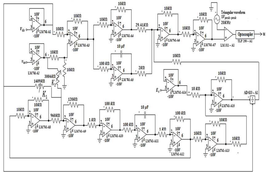
3.2. Experimental Results

For the sake of hardware implementation, further proportional and integral actions were introduced in Equation (31) to give
u = x 2 d s   E s V d s K p v o s V d s K i v o s τ V d s d τ
where   K p and K i are the positive constants. Figure 4 shows the circuit diagram of the proposed control scheme. Here, the division function was implemented using the AD633 chip (Wilmington, MA, USA). The proportional and integral gains used were K p = 0.34 and K i = 5 , respectively.
Figure 5a shows the output voltage of the converter for V d = 15   V . The response had a settling time of ~0.2 s with almost no overshoot. Figure 5b,c shows the converter response when R changed from R = 220   Ω   to R = 110   Ω   (vice versa) and from R = 220   Ω   to R = 1020   Ω   (vice-versa), respectively. The disturbances were rejected in ~0.2 s with a worst-case overshoot of ~1 V. Figure 5d shows the output voltage response in the presence of a reference voltage change from V d = 15   V to V d = 10   V and then back to V d = 15   V . These results clearly validate the suitability of the proposed controller for the step-up dc-dc converter.

3.3. Discussion on Results

Figure 3 and Figure 5 clearly illustrate the ability of the proposed controller to regulate the converter’s output voltage when disturbances in load, line, and reference voltage were introduced. As can be seen from Figure 3a, the transient response was critically damped with a settling time of ~0.025 s. Moreover, the load was changed by ~33% of its original value, the input was changed by 60% of its actual value, and in both cases the worst-case settling time was ~0.04 s with slightly less than 1 V of maximum overshoot. For the hardware prototype implementation of the proposed controller, extra proportional and integral actions were introduced to decrease the steady-state error owing to the parasitic resistances of the capacitor and inductor present in the circuit. This did not require the use of any additional sensing circuitry, and the control scheme can be realized using only an output voltage feedback sensor. As can be seen from Figure 5a, the settling time of the transient response was ~0.2 s with almost no overshoot. Moreover, the worst case settling time for ~500% change in the load resistance was around ~0.2 s with ~1 V of maximum overshoot.

4. Conclusions

The detailed design of a new output feedback controller for the dc-dc boost converter was presented. To this end, a controller structure satisfying the stability conditions was derived, and tuning guiding principles were given. The output voltage of the step-up converter was regulated directly despite the non-minimum phase dynamic response of the open-loop system. Moreover, the proposed controller avoids the possibility of saturation in the control signal as there is no chance of division by zero. Additionally, the closed-loop system has only one equilibrium point which is always stable. Simulation and experimental results also verify the output feedback controller’s ability to give robust response in the presence of parameter variations.

Author Contributions

Conceptualization, S.C.; methodology, S.C. and C.-Y.C.; software, S.C. and W.J.; validation, S.C., C.-Y.C. and W.J.; formal analysis, S.C.; investigation, S.C. and W.J.; resources, S.C., C.-Y.C., and S.S.R.; writing—original draft preparation, S.C.; writing—review and editing, S.C., C.-Y.C. and S.S.R. All authors have read and agreed to the published version of the manuscript.

Funding

The research received no external funding.

Conflicts of Interest

The authors declare no conflict of interest.

References

  1. He, X.; Li, W. Review of nonisolated high-step-up dc/dc converters in photovoltaic grid-connected applications. IEEE Trans. Power Electron. 2011, 58, 1239–1250. [Google Scholar]
  2. Wu, G.; Ruan, X.; Ye, Z. Review of nonisolated high-step-up dc/dc converters in photovoltaic grid-connected applications. IEEE Trans. Ind. Electron. 2015, 62, 383–393. [Google Scholar] [CrossRef]
  3. Ahrabi, R.R.; Ardi, H.; Elmi, M. A novel step-up multiinput dc–dc converter for hybrid electric vehicles application. IEEE Trans. Power Electron. 2017, 32, 3549–3561. [Google Scholar] [CrossRef]
  4. Sira-Ramirez, H.; Perez, R.; Ortega, R.; Garcia, M. Passivity-based controllers for the stabilization of DC-to- DC power Converters. Automatica 1997, 33, 499–513. [Google Scholar] [CrossRef]
  5. Alvarez-Ramirez, J.; Perez, G.E. Stability of current-mode control for dc–dc power converters. Syst. Contr. Lett. 2002, 45, 113–119. [Google Scholar] [CrossRef]
  6. Cervantes, I.; Garcia, D.; Noriega, D. Linear multiloop control of quasi-resonant converters. IEEE Trans. Power Electron. 2004, 18, 1194–1201. [Google Scholar] [CrossRef]
  7. Chan, C.Y. A nonlinear control for dc-dc power converters. IEEE Trans. Power Electron. 2007, 22, 216–222. [Google Scholar] [CrossRef]
  8. Chincholkar, S.H.; Chan, C.Y. Investigation of current-mode controlled cascade boost converter systems: Dynamics and stability issues. IET Power Electron. 2016, 9, 911–920. [Google Scholar] [CrossRef]
  9. Chan, C.Y.; Chincholkar, S.H.; Jiang, W. Adaptive current-mode control of a high step up dc-dc converter. IEEE Trans. Power Electron. 2017, 32, 7297–7305. [Google Scholar] [CrossRef]
  10. Chan, C.Y.; Chincholkar, S.H.; Jiang, W. A modified fixed current-mode controller for improved performance in quadratic boost converters. IEEE Trans. Circuits Syst. 2020, 67, 2014–2018. [Google Scholar] [CrossRef]
  11. Jiang, W.; Chincholkar, S.H.; Chan, C.Y. A Comparative Study of Adaptive Current-Mode Controllers for a Hybrid-type high-order Boost Converter. IET Power Electron. 2018, 11, 524–530. [Google Scholar] [CrossRef]
  12. Tan, S.C.; Lai, Y.M.; Tse, C.K. General design issues of sliding- mode controllers in dc-dc converters. IEEE Trans. Ind. Electron. 2008, 55, 1160–1174. [Google Scholar]
  13. López-Santos, O.; Martínez-Salamero, L.; García, G.; Valderrama-Blavi, H.; Mercuri, D.O. Efficiency analysis of a sliding-mode controlled quadratic boost converter. IET Power Electron. 2013, 6, 364–373. [Google Scholar] [CrossRef]
  14. López-Santos, O.; Martínez-Salamero, L.; García, G.; Valderrama-Blavi, H.; Sierra-Polanco, T. Robust sliding-mode control design for a voltage regulated quadratic boost converter. IEEE Trans. Power Electron. 2015, 30, 2313–2327. [Google Scholar] [CrossRef]
  15. Chincholkar, S.H.; Jiang, W.; Chan, C.Y. A modified Hysteresis-modulation-based Sliding Mode Control for Improved Performance in Hybrid Dc-Dc Boost Converter. IEEE Trans. Circuits Syst. 2018, 65, 1683–1687. [Google Scholar] [CrossRef]
  16. Chincholkar, S.H.; Jiang, W.; Chan, C.Y. A Normalized Output Error-based Sliding-Mode Controller for the Cascade boost converter. IEEE Trans. Circuits Syst. 2020, 67, 92–96. [Google Scholar] [CrossRef]
  17. Tan, S.C.; Lai, Y.M.; Nagy, I.; Tse, C.K. A unified approach to the design of PWM-based sliding-mode voltage controllers for basic DC-DC converters in continuous conduction mode. IEEE Trans. Circuits Syst. I Reg. Papers 2006, 53, 1816–1827. [Google Scholar]
  18. Tan, S.C.; Lai, Y.M.; Tse, C.K.; Wu, C.K. A pulsewidth modulation based integral sliding mode current controller for boost converters. In Proceedings of the 37th IEEE Power Electronics Specialists Conference, Jeju, Korea, 18–22 June 2006. [Google Scholar]
  19. Tan, S.C.; Lai, Y.M.; Tse, C.K. Indirect sliding mode control of power converters via double integral sliding surface. IEEE Trans. Power Electron. 2008, 23, 600–611. [Google Scholar]
  20. Chincholkar, S.H.; Chan, C.Y. Design of fixed-frequency pulse-width-modulation based sliding-mode controllers for the quadratic boost converter. IEEE Trans. Circuits Syst. 2017, 64, 51–55. [Google Scholar]
  21. Chincholkar, S.H.; Jiang, W.; Chan, C.Y. An Improved PWM-based Sliding-Mode Controller for a Dc-Dc Cascade Boost Converter. IEEE Trans. Circuits Syst. 2018, 65, 1639–1643. [Google Scholar] [CrossRef]
  22. Chan, C.Y. Simplified parallel-damped passivity-based controllers for dc-dc Converters. Automatica 2008, 44, 2977–2980. [Google Scholar] [CrossRef]
  23. Son, Y.I.; Kim, I.H. Complementary PID controller to passivity- based nonlinear control of boost converters with inductor resistance. IEEE Trans. Control Syst. Technol. 2012, 20, 826–834. [Google Scholar] [CrossRef]
  24. Nise, N. Control Systems Engineering; John Wiley & Sons, Inc.: Hoboken, NJ, USA, 2009. [Google Scholar]
Figure 1. Boost converter circuit.
Electronics 10 00493 g001
Figure 2. Phase diagram of Equation (29) using   E = 5   V ,   V d = 15   V ,   C = 100   μ F , K 1 = 0.08515 , and   K 2 = 0.03993 .
Electronics 10 00493 g002
Figure 3. System simulation responses: (a) transient output response (solid line) and control signal (dotted line), (b) output response and inductor current waveform for change in the load resistance from R = 220   Ω to R = 150   Ω (and vice-versa), (c) output response and inductor current waveform for change in the load resistance from R = 220   Ω to R = 330   Ω (and vice-versa), and (d) output response and control signal waveform for change in the input voltage from E = 5   V to E = 8   V (and vice-versa).
Electronics 10 00493 g003
Figure 4. Circuit diagram of the output feedback controller implementation.
Electronics 10 00493 g004
Figure 5. System response: (a) transient output voltage response for V d = 15   V , (b) output voltage response for change in the load resistance from R = 220   Ω to R = 110   Ω   and vice versa, (c) output voltage response for change in the load resistance from R = 220   Ω to R = 1020   Ω   and vice versa, and (d) output voltage response for change in the reference voltage from V d = 15   V to V d = 10   V and then back to V d = 15   V .
Electronics 10 00493 g005
Publisher’s Note: MDPI stays neutral with regard to jurisdictional claims in published maps and institutional affiliations.

