Article

Three-Phase PWM Voltage-Source-Inverter Weight Optimization for Aircraft Application Using Deterministic Algorithm

1
Univ. Grenoble Alpes, CNRS, Grenoble INP, G2Elab, 38000 Grenoble, France
2
Safran Tech, 78117 Châteaufort, France
*
Author to whom correspondence should be addressed.
Electronics 2020, 9(9), 1393; https://doi.org/10.3390/electronics9091393
Submission received: 11 August 2020 / Revised: 25 August 2020 / Accepted: 26 August 2020 / Published: 28 August 2020
(This article belongs to the Special Issue Multifaceted Applications of Power Electronics)

Abstract

:
In this paper, a design by optimization process is used to size a 10-kW three-phase pulse width modulation (PWM) inverter for aeronautic application. The objective function is the converter weight, which has to be minimized. Sizing constraints are the efficiency, alternating current (AC) and direct current (DC) harmonics, and thermal constraints on all devices. A deterministic algorithm is chosen since it allows obtaining quick results and dealing with a large number of variables. All equations are analytical, in order to comply with this gradient-based optimization strategy, which imposes the derivability of the models. Several optimization results using different AC inductor solutions (iron powder and ferrite) are compared. The optimized converters were built and tested experimentally to verify their performances. Semiconductor and inductor losses were measured accurately using calorimetric test benches. The optimality of the solutions was carefully verified by changing parameters.

1. Introduction

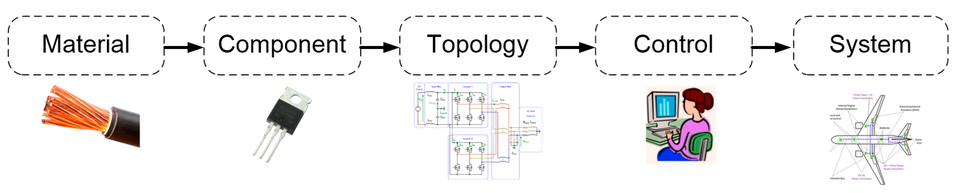
The tremendous development of electric transportation, such as electric vehicles and more electrical aircraft, drives innovation for power electronic converters. These new applications require better performance, in terms of weight, volume, cost, losses, failure rate, and development time [1]. Many performance indices can be currently improved thanks to technological breakthroughs, especially on active devices. However, the performance of a converter results from a global trade-off among devices, topology, and control, in strong interaction with the system requirements (Figure 1). A sequential approach in the design may, therefore, lead to sub-optimal results, because a global optimum is not simply the sum of subsystem optima [2]. For example, the switching frequency has an opposite impact on the sizing of the semi-conductors and on the design of a low-frequency filter. Solving all trade-offs simultaneously is the role of a power electronics expert, but the space of solutions is so wide that optimization tools can really be helpful to compare fairly candidate solutions or technologies.
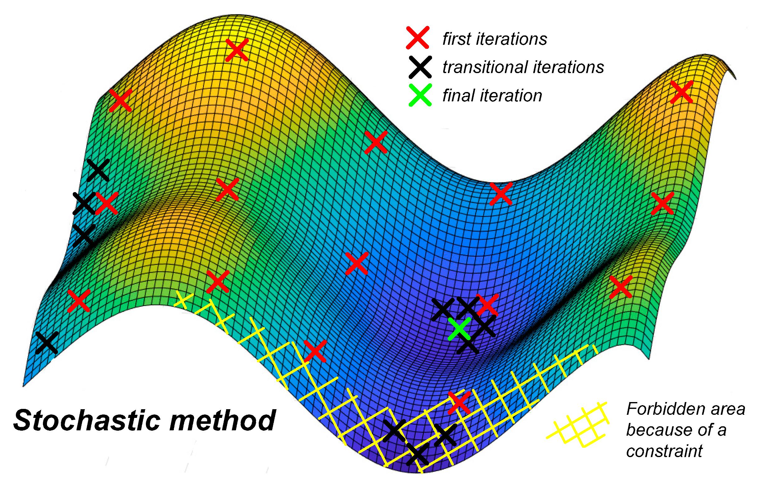
Many works already dealt with design tools for pulse width modulation (PWM) inverters with optimization methods. Several of them used stochastic methods, as illustrated by Figure 2. In Reference [3], the NSGA II algorithm (Non-dominated Sorting Genetic Algorithm II) [4] was used to choose the best topology and size an inverter realized with power module technology. A design space analysis was refined in Reference [5] to size an output filter of a 10-kW converter. Reference [6] minimized an LCL (inductor-capacitor-inductor) filter using stochastic methods coupled with circuit and finite elements method (FEM) simulations. In Reference [7], a method was used to reduce the number of potential design combinations by 99%, to achieve a reasonable computing time. A computer-aided EMI (ElectroMagnetic Interference) filter design procedure applied to PWM inverters was introduced in Reference [8], with a sequential approach.
The use of precise models, such as FEM or time simulations included in an optimization algorithm, can give very accurate results, but usually results in the need for a lot of computation time, while it may not be able to handle many constraints.
These limitations are a real drawback in the first steps of a project, when the specifications often change and when preliminary results are quickly required. Often, the expertise of the engineer is the only way to take the first decisions.
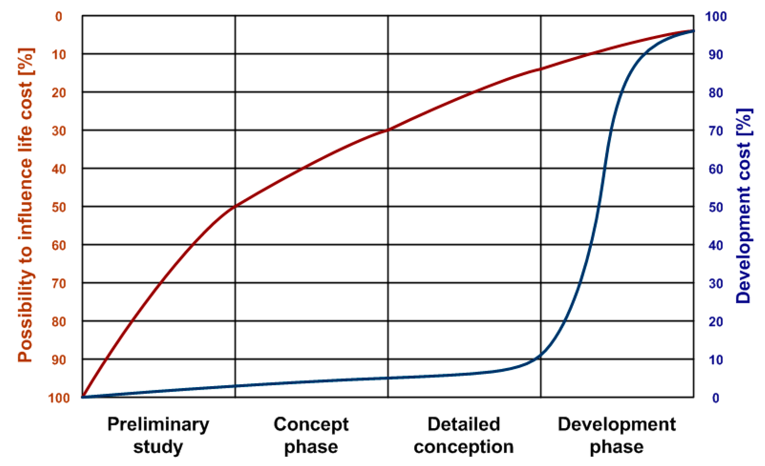
Deterministic or gradient-based algorithms are very powerful to explore wide spaces of solutions with a large number of constraints in a small amount of time. This is the reason why they are a good alternative to stochastic algorithms in the pre-design step of a project, to help the designer in quickly exploring a wide range of solutions. It was demonstrated in Reference [9] how relevant it is to take good decisions in the preliminary study phase (Figure 3). The brown axis indicates that, at the beginning of the project, everything can influence life cost. However, after the preliminary phase, many decisions are taken (constraints and topology choice) which decrease the size of the solution space (halved according to Reference [9]).
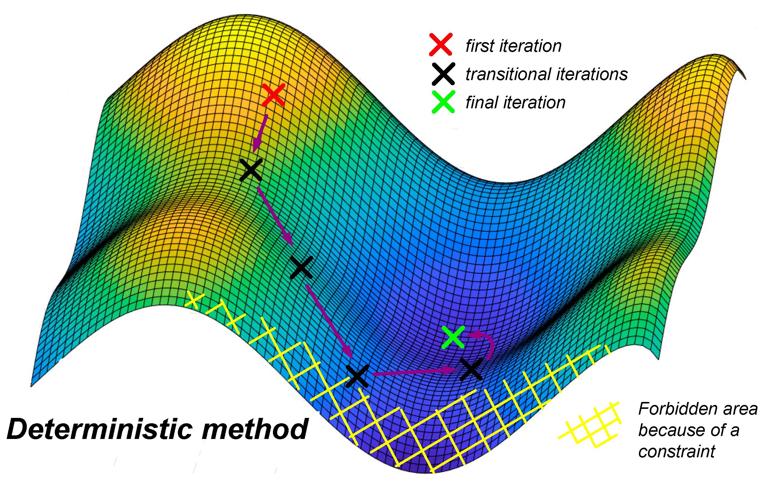
Figure 4 illustrates an optimization process using a deterministic algorithm. Computing the gradients of the system allows the algorithm to converge quickly to the optimal solution, easily avoiding spaces where constraints are not respected. It is a significant advantage compared to stochastic algorithms, because many constraints guide the design of power electronic converters. Furthermore, deterministic algorithms can handle more variables than stochastic ones. The alternative is to provide derivable models for all phenomena involved in the converter design. Since a possible drawback of gradient-based algorithms is to be stuck in local optima, a multi-start process can be added to the optimization strategy, in order to automatically change the optimization starting point, if the result is sensitive to the initial conditions.
Stochastic algorithms can also be used to obtain optimization results. The advantage is that they are compatible with any kind of model formulation (i.e., they do not need to be derivable); therefore, precise models such as time domain simulations and finite elements can be used. However, processing time and potential convergence difficulties are to be expected, especially in a wide space of solutions, where parameters can take multiple values. Indeed, stochastic algorithms have difficulties taking into account a large number of constraints. These stochastic algorithms may be used in the final design steps, rather than in the pre-design step. Each algorithm should be used during the appropriate stage of the project.
The design process is developed under a dedicated optimization framework [10], which is able to automatically differentiate the equations. Automatic code differentiation is a real advantage for deterministic optimization because it enables the algorithm to easily converge to the optimal solution. Since many parameters are discrete and, thus, non-derivable, we propose a projection in a so-called “imaginary space”, which is fully continuous [11]. The turn number of a winding is, therefore, not an integer, while all values of capacitance can be reached even if they are not available in a catalog. The optimization result is, thus, a kind of theoretical optimum, which is often sufficient in the pre-sizing step of a project [11], and which allows fairly and quickly comparing two solutions.
Having a mathematical mapping of the space of solution allows analyzing the impact of the variables on the design. As the models are continuous, it is possible to plot sensitivity curves showing, for example, the impact of an input variable on several output variables. For example, the designer can understand which constraint is limiting in the design and maybe investigate solutions to overcome this constraint.
In this paper, it is illustrated how to use gradient-based algorithms, using the example of a PWM voltage source inverter. The aircraft objective is to minimize the converter weight. The system level and technological constraints on the devices are considered. The models used for the optimization are briefly presented, and the results are discussed. Experimental validations of the optimization result are also presented.

2. Analytical Models Suitable for Deterministic Optimization

2.1. Topology and Specifications

This study considers the design of a direct current (DC)/alternating current (AC) converter with aeronautical constraints. The converter is sized for maximum power, under constant DC and AC voltages, as specified in Table 1. According to these specifications, the three-phase voltage-source-inverter topology is selected (Figure 5). A bipolar PWM modulation method is used for the control of the MOSFETs (Metal Oxide Semiconductor Field Effect Transistor). Automatically changing the PWM strategy is not compatible with the choice of using derivable models, and this has to be performed for each individual case. A comparison of different PWM modulations and their impact on the inverter design were detailed in Reference [6]. The inverter includes an LC (inductor-capacitor) filter on the DC and AC sides to guarantee low harmonic distortion on both DC and AC grids. The DC grid is assumed perfect (with a constant DC voltage source). The AC grid is represented as a balanced three-phase charge with a variable power factor. For this study, the charge is considered as a pure resistance, but the design tool can handle a variable power factor. In the studied configuration, the middle point of the DC bus is connected to the neutral point of the AC side, as is the case in an aircraft through aluminum skin.
In addition to Table 1, the following constraints were added, as summarized in Table 2:
  • Maximum junction temperature for semiconductor devices, maximum RMS current in capacitors, maximum loss density in inductors;
  • Power quality requirements (total harmonic distortion on AC side; voltage and current ripple on DC side);
  • User requests (efficiency, cost, etc.).
The main constraints are listed in Table 2. For the optimization, some constraints were added to ensure the feasibility of the realization. For example, the number of windings for an inductor has to fit the winding area. Finally, some constraints allow solving implicit equations, as explained in Section 2.2. No thermal models are implemented on passive devices, because they are too dependent on technological choices, which are not mandatory for a pre-design tool. Therefore, other indicators were chosen to reflect the thermal constraints: volumetric losses for DC and AC inductors; maximum RMS current for DC and AC capacitors.
The upcoming sections summarize the main models developed for inverter optimization. To be compliant with deterministic optimization, analytical formulations were chosen. A detailed survey of power electronics analytical models suitable for optimization was provided in Reference [12]. A synoptic view of the problem, linking input parameters, which are free, and output parameters, which are constrained, is given in Figure 6.
All the equations related to the developed models were written in the optimization tool. The algorithm recognizes that all the computed parameters (on the left-hand side of the equation) are output parameters. The remaining variables are input variables. Input variables in blue in Figure 6 can either be fixed by specification (as the nominal power) or vary between a minimum and a maximum value chosen by the designer. The output variables can be set as free, especially for intermediate parameters used in sub-models, or constrained. One variable was chosen as the minimization goal: the total weight.
This work takes low-frequency filters and standards into account, including THD and ripple constraints. A conducted EMI defined by the DO160 standard between 150 kHz and 30 MHz is a problem on its own and, as such, was not considered in this work. EMI is difficult to address with deterministic methods because a constraint should be added for every single harmonic in the frequency range, which represents nearly 75,000 constraints. Reference [13] illustrated this topic.

2.2. Semi-Conductor Losses

According to the aeronautical specifications given in Table 1 and Table 2, this work considered silicon carbide (SiC) MOSFETs and a diode. The voltage rating was 1200 V. The loss evaluation accounts for conduction losses, including reverse conduction of the MOSFETs. This requires calculating the RMS and average current in the MOSFET and the diode [14]. Losses also depend on the PWM control strategy, which was investigated in Reference [15].
The dependence of the on-state resistance of the MOSFET (Rdson) on the variation of temperature is taken into account. According to the manufacturer datasheet, Rdson increases in a quadratic way with the temperature (Equation (1)). The junction temperature Tj is evaluated using the thermal resistance of the semiconductor package (given in the datasheet) and of the heatsink, as well as the value of losses, which depends on Tj for conduction losses. To solve this implicit equation in optimization, an initial Tj,init and a final Tj,final are defined. In other words, the losses are evaluated at temperature Tj,init, and the thermal resistance allows computing Tj,final. A constraint is added in order to minimize the difference between Tj,init and Tj,final, which guarantees the convergence of the junction temperature.
Rdson ( T J ) = a . T J 2 + b . T J + c .
Switching losses are evaluated using the usual quadratic approximation (Equation (2)), with a, b, and c coefficients interpolated from the manufacturer datasheet. The dependence of switching energies on temperature is not considered, as this influence is low for SiC MOSFETs.
E ( I ) = a . I 2 + b . I + c .
The values of conduction and switching losses depend on the current rating of the device; on-state behavior obviously changes with the surface of the dies, and switching energy also varies with area, since capacitances are increased. These phenomena were considered using a continuous variation, with the area of the device as an input parameter. Therefore, the current rating (or die area) becomes an optimization parameter. The thermal resistance of the semiconductor package also changes with die area.
The semiconductors are cooled with a water plate, connected to the global cooling of the aircraft. Therefore, as the exchange is supposed infinite, the weight of this cooling plate does not change with the amount of semi-conductor losses, as would be the case with a local heatsink. This is why a detailed cooling model was not integrated in the pre-design tool. In other cases, a more detailed cooling system model can be useful. A forced air cooling model, suitable for optimization, was used in Reference [16], adapted from the work of Reference [17].

2.3. Harmonic Calculation

The PWM spectrum is expressed with a double Fourier series leading to Bessel functions (Equation (3)) [18]. The output voltage Vout is then computed using the transfer function TF of the filter, including the LC filter and the load (Equation (4)) (Figure 7). The THD is then computed using Equation (5).
V PWM ( k . m + p ) = 2 . V DC π . k sin ( π k + p 2 ) . J n ( p , π k . r 2 ) ,
with J n ( p , k ) p order, first-type Bessel functions.
V OUT ( f ) = TF ( f , L AC , C AC , R load , L load ) . V PWM ( f ) .
THD ( % ) = 100 h = 2 V OUT ( h ) 2 V OUT ( 1 ) .
The AC capacitor current is computed knowing the output voltage spectrum VOUT at the terminals of the capacitor and its impedance. This model is valid with a variable load power factor, which is set to 1 in the studied example.
On the DC side (Figure 8), the RMS current in a DC capacitor, the DC bus voltage ripple, and the DC current ripple in the generator are considered. The current spectrum in the DC side of the converter is useful to evaluate the DC voltage and current ripples, as well as the RMS DC capacitor current. It is worth noting that the contribution of the AC current ripple is considered in this analytical expression [19], which is important during optimization.

2.4. Inductor Models

The model parameters are based on a geometrical description of the component, whose dimensions can change continuously, in order to have a derivable model. Manufacturing constraints such as various ratios between geometrical parameters can be considered. The turn number is another parameter considered as a real number to keep derivability.
Litz wire technology was used to decrease copper losses due to frequency effects. The Dowell method [20] enables calculating the variation of the resistance with the frequency, which can be adapted to toroid core shapes [21,22] (Equation (6)).
R AC R DC = x . ( sh ( 2 x ) + sin ( 2 x ) ch ( 2 x ) cos ( 2 x ) + 2 3 ( Nb layer 2 1 ) sh ( x ) sin ( x ) ch ( x ) + cos ( x ) ) ,
where x = π 2 Φ strand Δ , Φ strand is the diameter of a Litz wire strand, and Δ is the skin depth, depending on the frequency.
Three kinds of magnetic materials were considered for this study. The first core materials were iron-alloyed powders, with toroid shapes. In this case, the model took into account a variable saturation state of the core. For example, the core can saturate during the current peak, which leads to a local increase of the current ripple. The second kind of core was a ferrite core. In comparison to powder cores, a constraint was added on the saturation of the ferrite core, in order to not exceed the saturation induction given by the manufacturer. This choice was made assuming that the B–H curve is very linear between 0 T and the saturation induction, whereas there was no interest in working after the saturation induction. A comparison between both kinds of ferrite material is discussed in Section 5.2.
The saturation phenomenon is important when optimizing the weight, since inductors contribute to a great part of the total converter weight. The full method was described in Reference [23]. It consists of calculating the induction ripple ΔB. The voltage at the terminals of the inductor is evaluated during a high-frequency period and integrated according to Lenz law, leading to Equation (7). This induction ripple is used in the iGSE (improved Generalized Steinmetz Equation) model [24] to compute iron losses (Equation (8)).
Δ B HF ( t ) = V in 2 V out rms 2 . sin ( ω . t ) N . S . f sw 1 + r . sin ( ω . t ) 2 ,
where N is the number of turns, and S is the magnetic surface.
P vol iGSE = 2 k i Δ B ( β α ) 1 T k Δ B HF ( k ) α . ( t off ( k ) t on ( k ) ) 1 α .
The magnetic field H0 is proportional to the low frequency current, according to Equation (9).
H 0 ( t ) = N l iron I out rms . 2 . sin ( ω grid . t ) .
The magnetic field ripple is calculated considering the saturation of the magnetic core (Equation (10)), which depends on time. The B–H curve is interpolated by an arctan function with magnetic core data. Differentiating this equation leads to the expression of the permeability, as a function of the magnetizing force (Equation (11)).
B ( μ r , H ) = K . arctan ( μ r . μ 0 . H K ) .
μ ( μ r , H ) = B ( μ r , H ) H = μ r . μ 0 1 + ( μ r . μ 0 . H K ) 2 .
Finally, the current ripple is computed in Equation (12). The RMS value of the current, composed of the grid frequency component and this ripple, is evaluated and used for copper losses.
Δ I HF ( t ) = l N Δ B HF ( t ) µ ( t ) ,
where l is the mean magnetic length of the core, and µ(t) is the permeability varying with the saturation of the core.
It was chosen to limit the windings on a single layer to decrease the parasitic capacitors and avoid EMC issues [25], even if this limited the space of solutions.

3. Optimization Result

3.1. Comparison of Different Solutions

The objective function was to minimize the converter weight, considering all system and device constraints. There was no priority management for the constraints. During the resolution, each constraint has to be respected. If this is not possible, the algorithm indicates which parameters were set to the limit values, helping the designer to relax some constraints.
Three main optimizations were carried out, with the same requirements given in Table 1 and Table 2. The first used an inductor made with a powder core, whereas the second used an inductor made with a ferrite core. Finally, the last optimization used a powder core, but with additional empirical constraints, according to some traditional “expert rules” that engineers could follow in the design of this inductor. These additional constraints included a limitation of the permeability drop at 80% of the nominal value (20% drop allowed), as well as a limitation of 20% of the current ripple in the inductor. The empirical constrained solution can be seen as the initial converter of this study. Global optimization takes into account the advantages and drawbacks of allowing variable saturation and AC current ripple in order to find a better solution.
Optimization was carried out with different efficiency targets, always with the aim of minimizing the weight. 
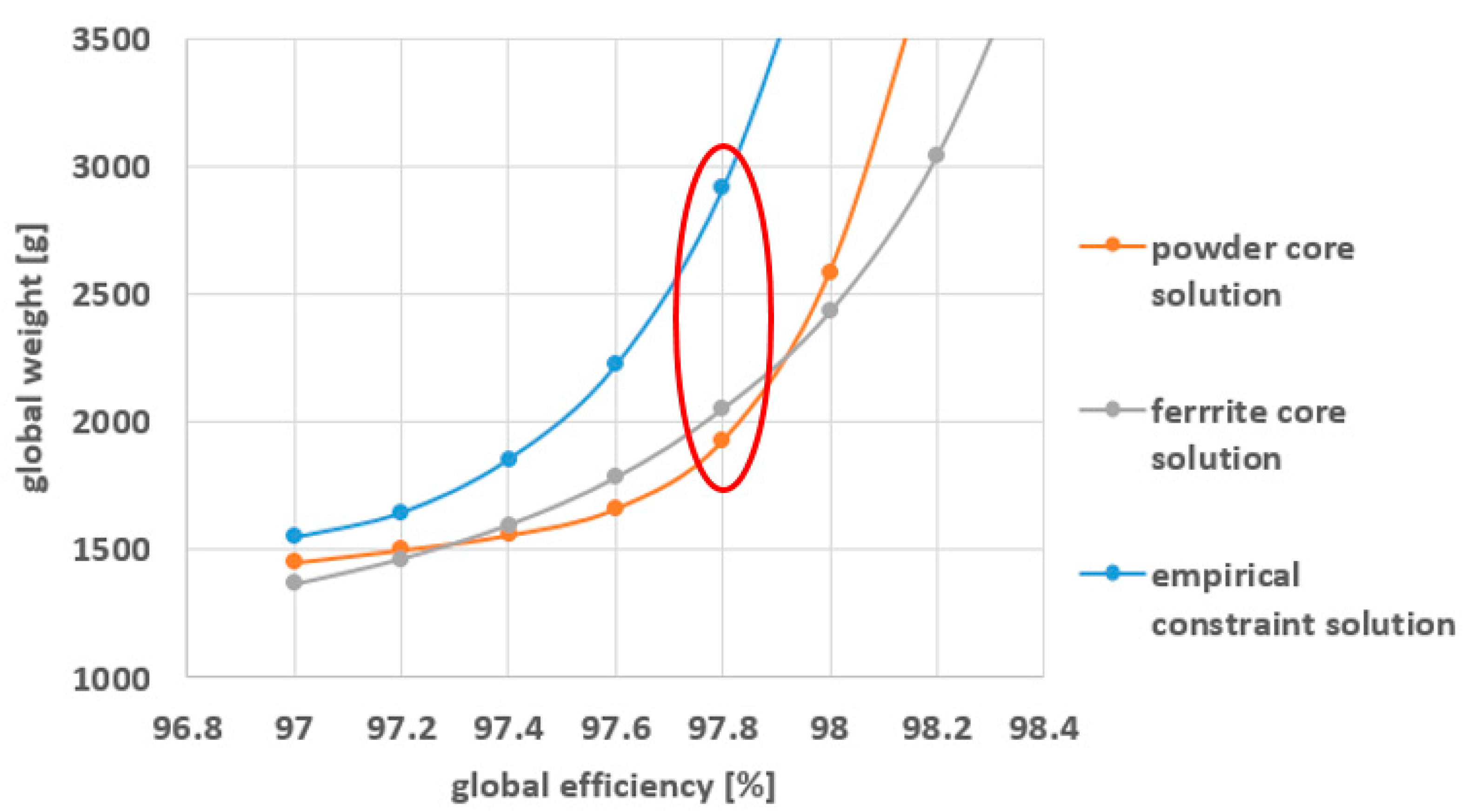
Figure 9 shows the weight-efficiency Pareto fronts for the three study cases. Solutions exist for lower and higher efficiencies, even if not displayed to keep balanced boundaries for the graphic.
The empirical constraint solutions were heavier than the others. This means that constraining the space of solutions with traditional rules was, in this case, inefficient to achieve an optimal design. Allowing a significant drop in permeability (higher than the usual 20%) with high current ripple would be useful in the design of a powder core inductor.
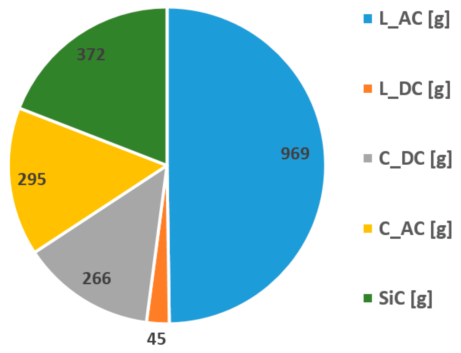
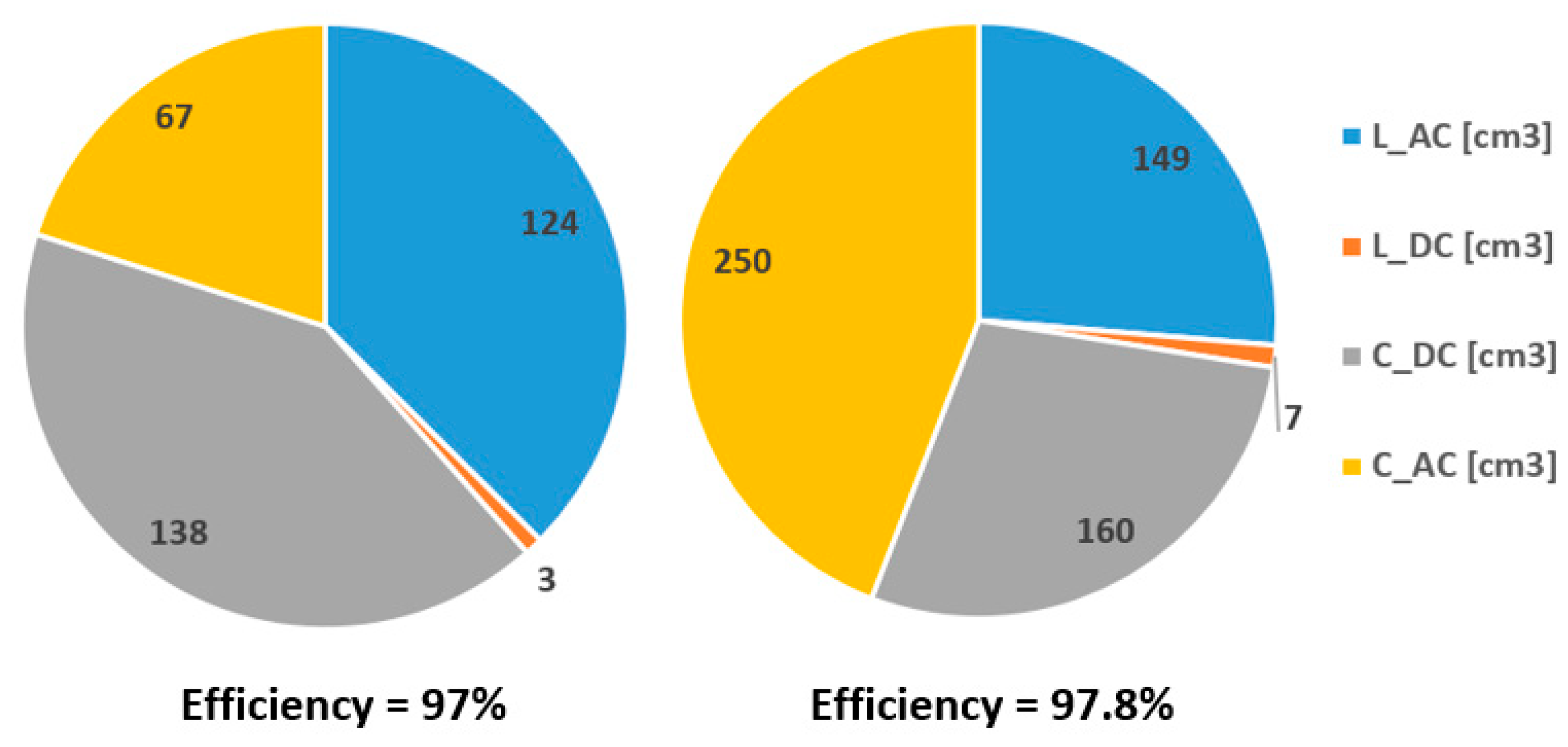
The weight repartition was similar for the three solutions. Figure 10 gives the weight distribution for the powder core solution at 97.8% efficiency. Inductor weight was computed using core and conductor weight, while capacitor weight used continuous interpolation of datasheets. The semiconductor weight was considered constant, since it is mainly a function of the package and almost independent of the die area. Obviously, in higher power, the package may be affected (several paralleled modules), but this was not necessary in this study.
It is clear that the AC inductor represented almost two-third of the global weight.
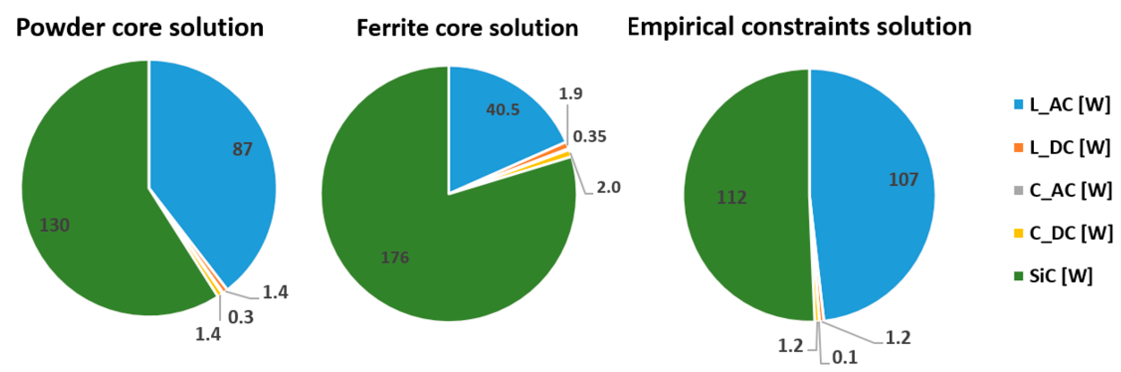
The powder core solution and the ferrite core solution gave similar results in terms of weight and efficiency. However, the details in the design were significantly different. The differences appeared in the choice of the optimal switching frequency and in the repartition of the loss to achieve 97.8% efficiency. The switching frequency was chosen at 52 kHz for the powder core solution, at 79 kHz for the ferrite core solution, and at 54 kHz for the empirical constraint solution. The distribution of losses is given in Figure 11. On the three charts, the sum of each loss contribution was equal to 220 W, according to the chosen efficiency point.
The main constraint in the design of a powder core inductor is the core losses, whereas it is saturation for the ferrite core inductor. This is why the powder core inductor had more losses than the ferrite core inductor. As the ferrite core inductor had fewer losses, the algorithm was able to increase the switching frequency to decrease the size of the LC filter. Increasing the switching frequency was possible because the increase in switching losses in the MOSFET was balanced by the decrease in core losses compared to the powder core design.
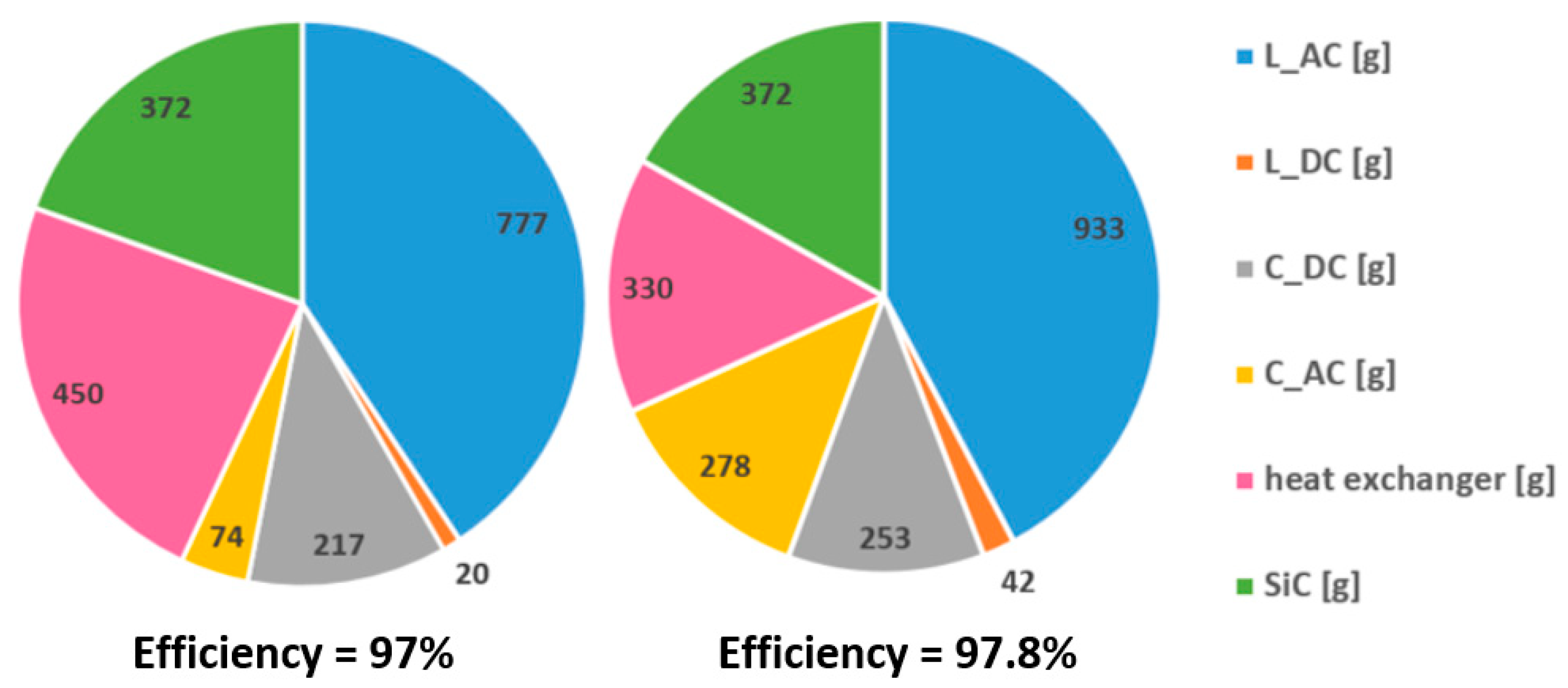
Other optimizations were carried considering the weight of the exchanger varying with the amount of loss to evacuate. A typical ratio of 1.5 kg of heat exchanger per 1 kW of loss was added, which is commonly used in aircraft systems [26]. The optimal weight distribution is shown in Figure 12 for two efficiency constraints.
Adding the heat exchanger weight penalized converters with a low-efficiency specification. The weight distribution in the converter with 97.8% was slightly different in comparison to Figure 10, because of the impact of the switching frequency on both active and passive components, which justifies the need for global optimization.
The component volumes, related to the two optimal points given in Figure 12, are shown in Figure 13. Compared to the weight charts, capacitors took a larger portion than the AC inductor, which is normal due to density differences. If the designer wants to minimize the volume instead of the weight, which is particularly useful in an automotive application, the design should be very different.
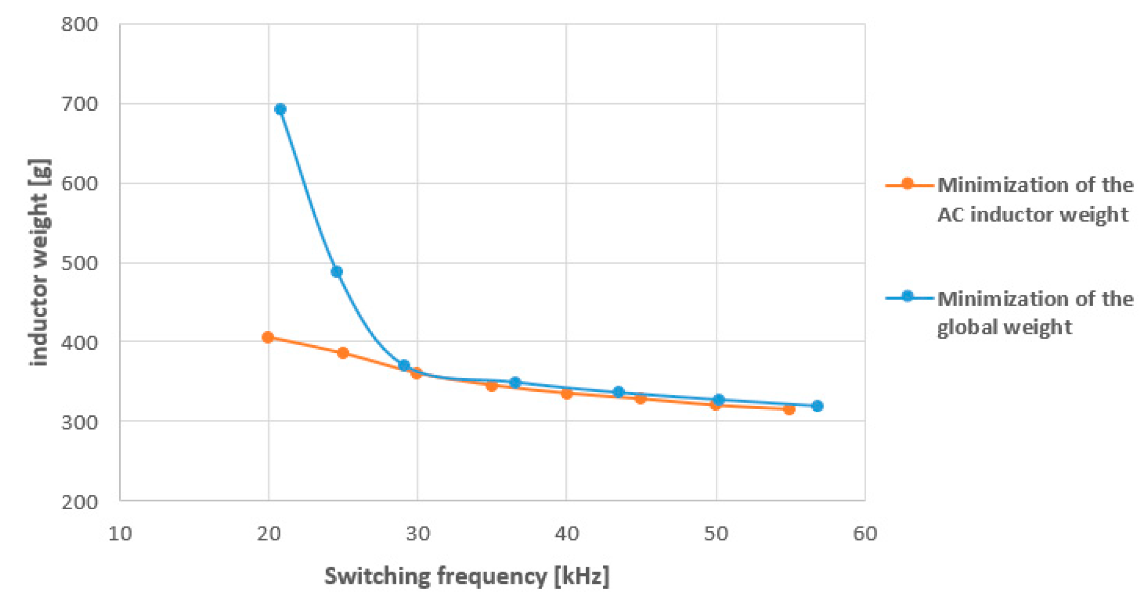
The design of the chosen example was very sensitive to the AC inductor. In this context, it would be possible to use a sequential design methodology, whereby the inductor is designed first, followed by the remaining components. However, this sequential methodology does not result always in the best converter, as illustrated hereafter. An AC inductor, optimized separately, was compared to the AC inductor optimized with the converter for different switching frequencies in Figure 14.
For high frequencies, the local inductor optimization was equivalent to the global design, because the inductor became the very constraining point. For low frequencies (high efficiencies), the two designs were different. This difference can be explained by two reasons:
  • When high efficiency is required, the AC current ripple should decrease to get lower losses. This is achieved by increasing the AC inductor value and, consequently, its weight.
  • For lower frequencies, filter cut-off frequencies should increase to respect ripples standards. The AC inductor value and weight increase.
  • Therefore, the lightest inductor is not necessarily the best choice for obtaining the lightest inverter, which justifies the use of a global methodology.
In the rest of the paper, to be consistent with the experimental validation, the heatsink was not included in the optimization objective function.

3.2. Sensitivity Analysis and Optimality Demonstration

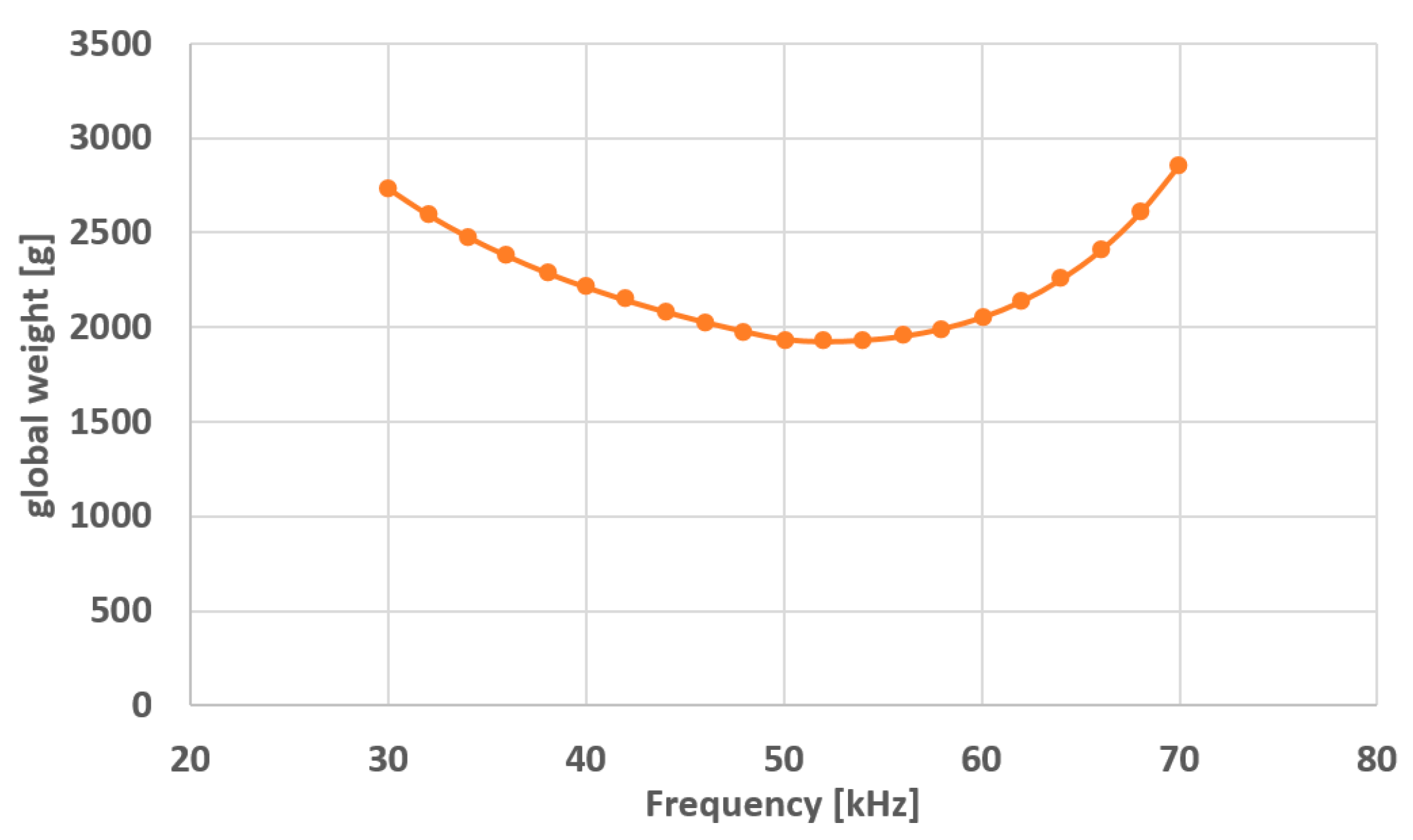
The optimality of the solution has to be checked to guarantee that the algorithm found the best solution. Thus, this paragraph validates the ability of the algorithm to find the optimal switching frequency. The switching frequency is only one of the variables of the design, but it is one of the most important for the whole converter, because it strongly affects the design of each component. For the following studies, the reference solution was the powder core solution.
The first study consisted of imposing different switching frequencies at the beginning of the optimization process (Figure 15). The optimal weight was found when the switching frequency was equal to 52 kHz, which is the same frequency found by the algorithm in the previous section. This means that the algorithm was able to choose the optimal switching frequency. Another conclusion with this graph is that shifting the optimal switching frequency from 20% (e.g., ±10 kHz) led to an average increase of 10% in the global weight. This study was carried out using some other parameters and gave equivalent results.
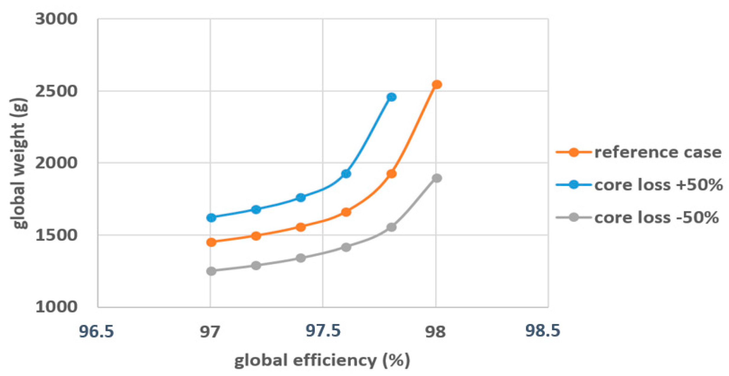
The results were obviously sensitive to model accuracy. This paragraph shows the impact of uncertainty in core losses on the total weight. Core loss was chosen because analytical models may lack precision due to the complex waveforms of PWM signals, impact of saturation, and DC bias. Figure 16 shows that increasing core losses of 50% led to an 11% increase in the total loss for low-efficiency constraints. In the case of high-efficiency constraints, the difference was higher, and some efficiency points could not be achieved. Decreasing core losses by 50% led to a 14% drop in the total loss, and higher efficiency could be achieved. It is possible to quantify the impact on the design of a given uncertainty using this model. This study can lead the designer to choose to improve the models with high uncertainty and with high impact on the result.
The final study consisted of shifting the switching frequency after the end of the optimization process. The global weight of the converter remained unchanged. Table 3 compares the main constraints of the following converters:
  • The optimal converter, with a switching frequency of 52 kHz;
  • The same converter, with a switching frequency of 42 kHz (−10 kHz);
  • The same converter, with a switching frequency of 62 kHz (+10 kHz).
The constraints of the optimal converter were always respected. Most of the constraints were really close to the limit value. The results in bold indicate that the parameter exceeded the limit value.
If the switching frequency decreased, many constraints were no longer respected, such as THD, hmax AC, ΔVDC, ΔIDC, and PTOT VOL AC. In addition, the RMS currents in both DC and AC capacitors increased, without reaching the limit. The explanation is simple; decreasing the switching frequency increased voltage and current ripples. This current ripple rise also increased the losses in the inductor. This was due to an increase in the induction ripple ΔB, which generated a global rise of core losses, even if the switching frequency decreased.
If the switching frequency increased, ripple constraints were not affected, but the efficiency requirement was no longer valid. Even if the inductor losses decreased slightly, semi-conductor losses increased because of commutation losses.
Therefore, if the switching frequency shifted from the optimal point, at least one of the constraints was no longer respected. This again justifies the optimization result found by the algorithm for the switching frequency.
Shifting the switching frequency by ±10 kHz led to an increase in the weight or a violation of one of the constraints. However, the new performances were really close to those of the optimal converter. This means that the solution found by the algorithm was robust to a shift in one of the parameters. An imprecision in input data for manufacturing reasons did not lead to a result far away from the predicted result.

3.3. From the Imaginary World to the Real World

A deterministic optimization algorithm, with a sequential quadratic programming (SQP) method [27], was used to solve the global inverter design. As the deterministic optimization needs differentiable parameters, some variables can have imaginary values. For example, the number of turns of a passive device can be a non-integer, while the capacitor value/core size may not be available for purchase. In other words, the algorithm gives a theoretical optimum, which is very useful in the pre-sizing step of a project, and which allows fairly and quickly comparing two solutions, i.e., the aim of this study.
Even if prototyping a converter was not the main goal of this optimization, a methodology was developed to obtain a real converter from the optimal solution in the imaginary world. This methodology enables finding a feasible converter nearest to the optimal converter. It consists of sequentially imposing the input parameters of the model. After assigning a value to the first variable, another optimization is carried to find the new optimal point, resulting in an iterative process.
Therefore, the process is a succession of value assignment and optimization. The general method consists of firstly assigning the discrete parameters with the highest impact on the design result or those limited to a few discrete references in a catalog. In this application, to build and test a real converter in order to validate the optimization results, we firstly fixed the SiC devices, for which availability was very poor, then the AC inductor core and wires, followed by the AC capacitor and DC capacitor, and finally the switching frequency. We performed this sizing process for the three converters with 97.8% efficiency underlined in Figure 9.

4. Test Benches

Among all the parameters to be checked to verify the optimization results, loss measurements of passive and active components were very challenging. Because of the switching waveforms, loss measurements using an electrical method (e.g., product of voltage and current) are not recommended. Therefore, calorimetric measurements were used. This section introduces the two calorimetric test benches for the measurement of semi-conductors losses and AC inductor losses.

4.1. Semi-Conductor Loss Measurement

The calorimetric measurement for semi-conductors losses was based on Equation (13), as presented in Figure 17.
Φ = Q . C p . Δ T ,
where Φ is the heat flow (W), Q is the water flow (kg/s), Cp is the water heat capacity (J/K/kg), and ΔT is the temperature difference between hot and cold water (K).
A dedicated set-up was used, based on a recirculating cooler, a water-cooled plate where the semiconductors were mounted, a Coriolis flowmeter, and thermocouples [28]. The maximum measurement error was estimated below 2%.
Before validating the main performances of the inverter, this bench was used to verify the switching energy with our gate driver. In buck configuration, losses were measured for different switching frequencies. Losses were plotted as a function of the switching frequency, where the slope is the total energy of the commutation cell, including turning off and turning on for the MOSFET, as well as the reverse losses in the diode, since it was part of the switching cell (even if it was small for a Schottky diode). This process was carried for three different switched currents to plot the green curve of Figure 18. The results were close to those given by the manufacturer.

4.2. Inductor Loss Measurement

The calorimetric method to measure the losses in an AC inductor is shown in Figure 19. It consisted of maintaining a constant temperature gradient between the oil and the environment. Oil was used in the calorimetric bench to ensure dielectric isolation, as the inductor was directly in contact with the fluid. The environment temperature was kept constant by an oven (controller 2). The oil temperature was regulated by a PI (Proportional Integral) controller, which controlled a heating resistor. When the inductor was heated, the controller decreased the power injected in R1 in order to keep a steady temperature. The difference in injected power between the beginning and the end of the test was equal to the inductor losses. This set-up was previously tested for determining inductor losses [29]. The maximum measurement error was estimated below 1%.

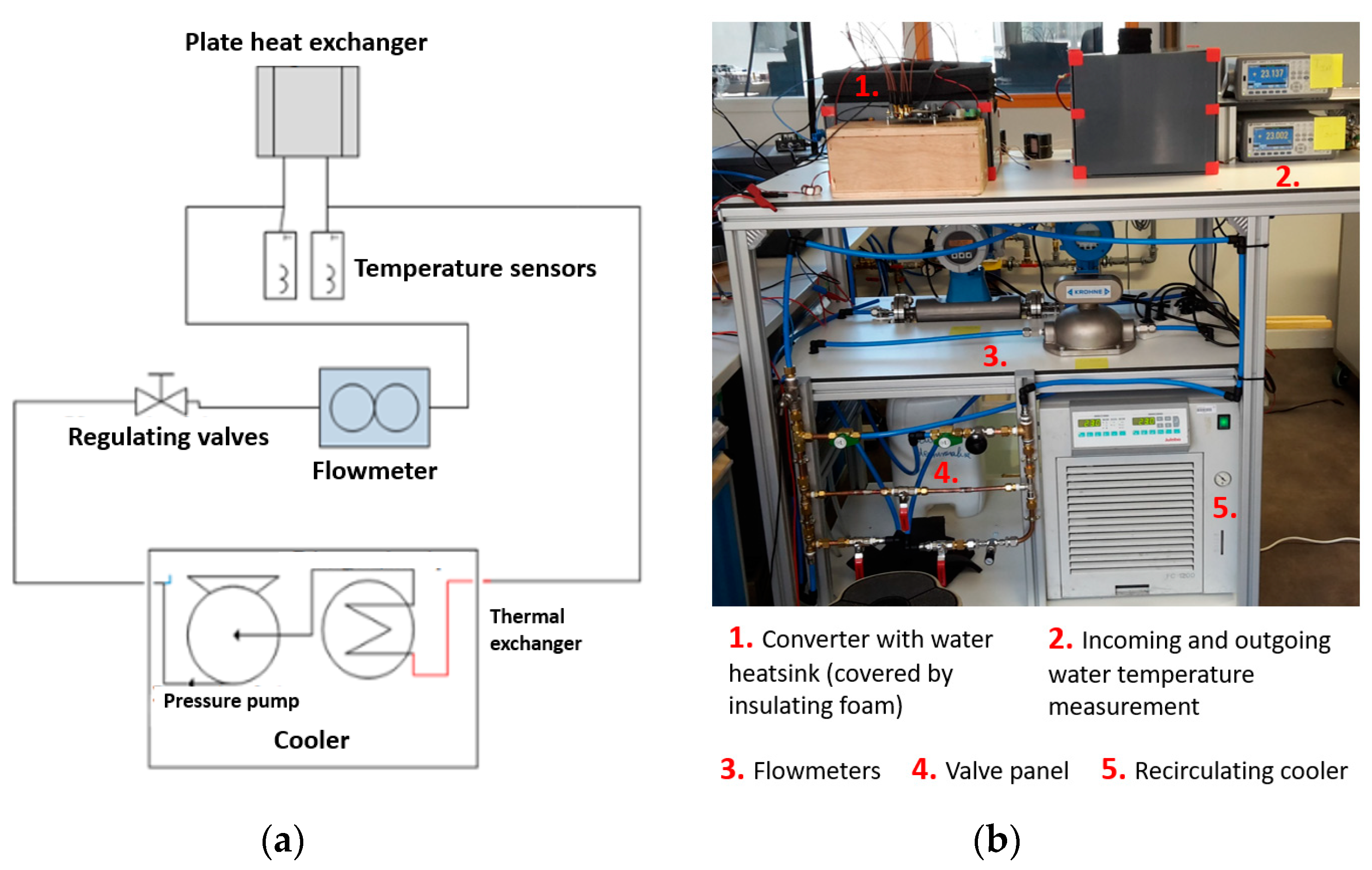
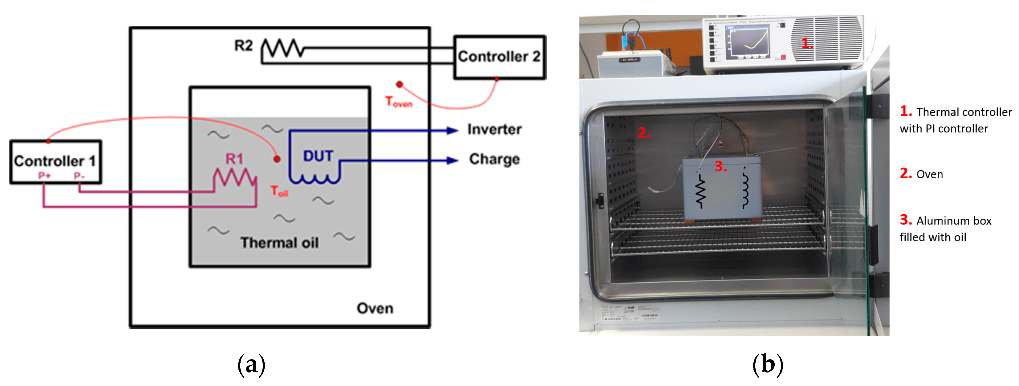
5. Experimental Validation of Optimization Results

The goal of this section is to check the validity of the optimization results and the models used in the optimization. As it is a pre-design tool, using only analytical equations, without simulation software or FEM tools, the accuracy of the results are not supposed to be as good as usual design models, but they allow solving a global design, by simultaneously considering all couplings inside the converter.
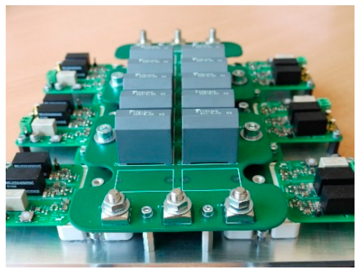
The three optimized converters were manufactured using the same common core shown in Figure 20. Due to the limited availability of SiC devices, the semiconductors were identical for each converter, while only passive elements and switching frequency were changed among the three converters, according to the optimization results after the discretization process explained in 
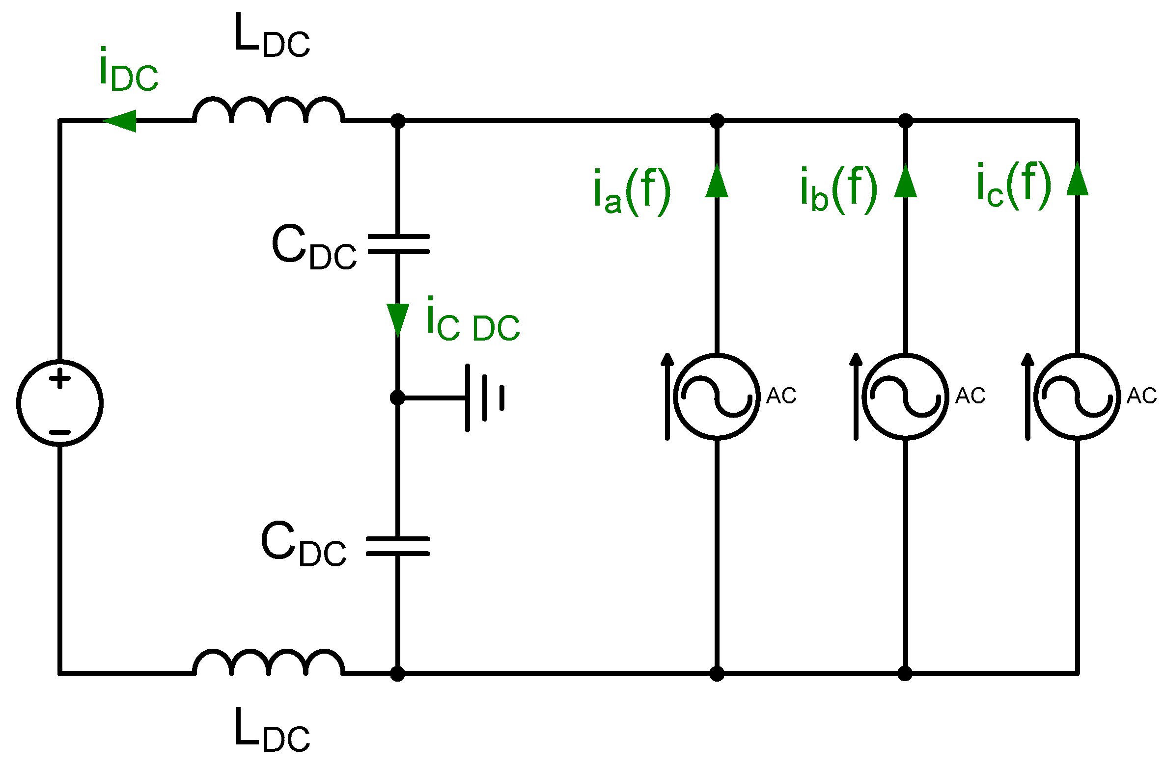
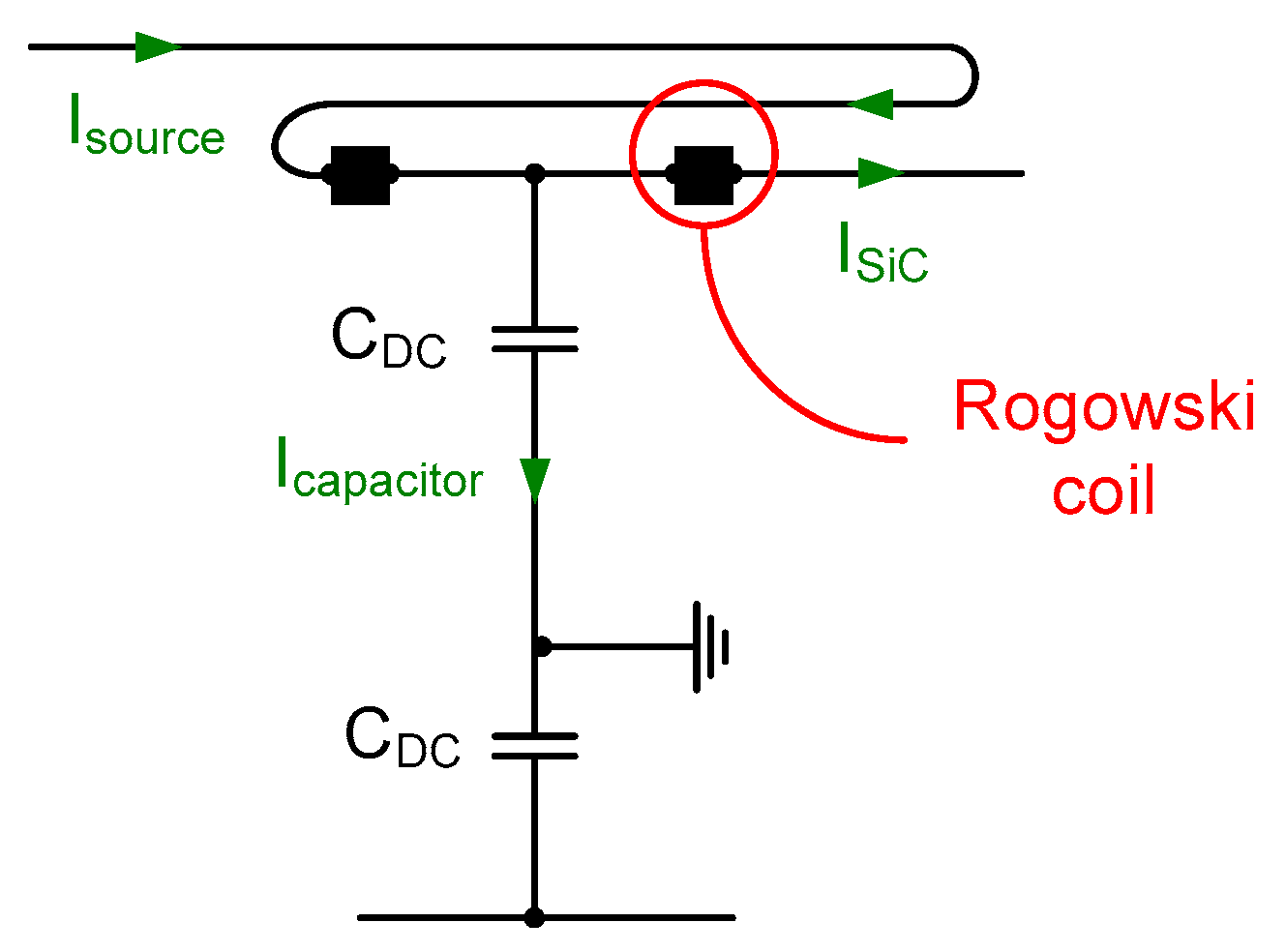
Section 3.3. One issue when experimentally validating some constraints is current measurement in the DC bus capacitors. Inserting a current sensor may modify the electrical path and change the measured current, especially in paralleled devices. It was decided to measure global current (Figure 21) with a Rogowski coil embracing (1) the connection between the DC capacitor bus board and the semi-conductor board, and (2) the DC current coming from the source.
With a proper wire orientation in the coil, the two currents were subtracting, resulting in the DC capacitor current.

5.1. Powder Core Solution

This solution used a KoolMu core with a relative permeability of 60. The choice of the material and permeability was done considering the designer experience and the availability of products on the market. It is also possible to optimize the choice of material and permeability with the tool [23]. Table 4 compares the optimization results with the main experimental measurements.
The comparison revealed few errors between the optimization results and the experiment. The error in the semi-conductor losses may have come from uncertainty in the manufacturer data. The main issue in the experimental results was the presence of low-frequency harmonics, which affected the measurement of ripples and THD. These harmonics came from the dead times between the control of the two MOSFETS in a phase leg. Low-frequency harmonics caused by dead time can be eliminated with an appropriate closed loop control [30,31]. Assuming that the closed loop control will not affect losses or high-frequency oscillations, the results are shown without taking into account the impact of these low-frequency harmonics.
The measured voltage THD and the maximum voltage harmonic were lower than what the model expected. This was due to the saturation of the inductance along the low-frequency period, which was considered in the worst case in the model; in the frequency model (Section 2.3), time-varying inductance was not considered, and the minimum value was used, which is the worst case.
Finally, DC voltage, current ripple, THD, and maximum AC voltage harmonic measurements were not precise and may have led to some errors, because the measure concerned a small percentage of the whole signal. Additional circuit simulations were carried out to verify that the converter respected these constraints.

5.2. Ferrite Core Solution

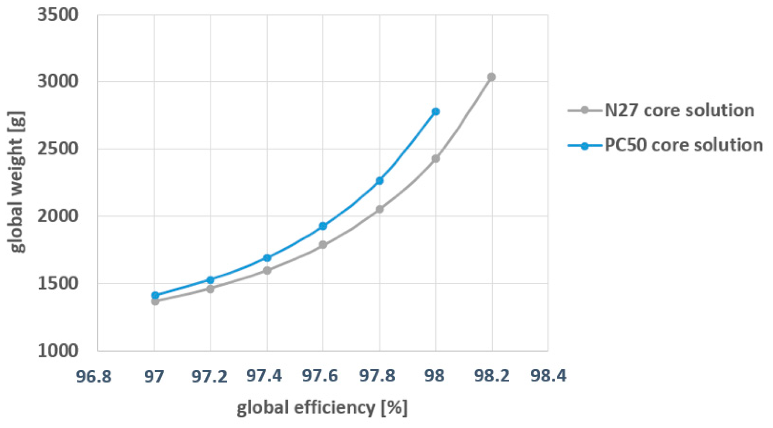
The choice of the ferrite core material was investigated with a preliminary study. Because of the use of an SiC device, high-frequency cores could be considered. Figure 22 shows two Pareto fronts with optimal solutions: one using N27 ferrite and one using PC50 ferrite, which is suitable for high-frequency applications (100–500 kHz).
At 97% efficiency, the optimal switching frequency was 130 kHz, while it was 60 kHz for 98% efficiency. At 130 kHz, results with PC50 material were equivalent to the results with N27. However, N27 material was better at 60 kHz, because the switching frequency was out of the scope of performance of PC50 material. Using a high-frequency core (PC50) in this application was not relevant because the switching frequency was not high enough, despite the use of an SiC device.
Consequently, N27 ferrite core was preferred for the experiment, with a PM shape. Results are shown in Table 5.
The experimental results were again close to the expectations. The same error in semi-conductor losses appeared. The model also underestimated the inductor losses. This was predictable because the conductors wound close to the air gap resulted in extra copper losses due to the magnetic field induced. The Dowell model was not suitable for this purpose, and a three-dimensional (3D) finite element simulation would be required to precisely estimate these losses. However, the error was not too critical (<20%) for a pre-design tool.

5.3. Empirical Constraint Solution

This solution used a KoolMu core with a relative permeability of 26. Decreasing the permeability from 60 to 26 compared to the optimal powder core solution was the best option to handle the additional constraints on the current ripple and the permeability drop. Comparisons between optimization result and experimental result are shown in Table 6.
The measurements carried out revealed very few differences compared to the optimization result. The global behavior of the converter was close to the two previous solutions, except that the converter was far heavier than the two others, which validated the optimization results. This confirmed that leaving freedom to the algorithm to explore a space of solution with high current ripple and some permeability drop allows obtaining better solutions, without scarifying converter performance.

6. Conclusions

A pre-design optimization method was presented and evaluated to design a three-phase PWM inverter for aircraft application. The tool uses a gradient-based algorithm, which allows considering a huge number of variables and constraints, which is not the case for usual design methods based on stochastic approaches. In the considered example, 20 variables and 20 constraints were handled. The method was able to provide quick results (less than 5 min) with acceptable accuracy, which is especially useful in the pre-design step of a project, where quick answers are needed.
Analytical models were used to be compatible with the gradient-based algorithm. Thus, the goal was to find or develop accurate and light analytical models for passive and active components, as well as to evaluate losses, ripples, and thermal constraints.
Many optimizations were carried out and illustrated with Pareto fronts. Different results were compared and discussed, in order to understand and confirm the choices of the algorithm.
Finally, experimental validations were presented. Two precise calorimetric benches were used to measure passives and actives losses. The measurements were compared to the optimization tool results. No significant differences were found, which justifies the accuracy of the developed method and models.
Further work will focus on the comparison of performances between different topologies (interleaved, multilevel) and may integrate constraints coming from the system level (EMC, mission profiles).

Author Contributions

Methodology, J.-L.S.; software, A.V. and A.D.; validation, A.V and A.D.; formal analysis, A.V and J.-P.F.; investigation, A.V.; resources, A.V., J.-P.F., J.-L.S., and C.G.; data curation, A.V.; writing—original draft preparation, A.V.; writing—review and editing, J.-L.S., J.-P.F., and C.G.; supervision, J.-L.S., J.-P.F., and C.G.; All authors have read and agreed to the published version of the manuscript.

Funding

This research was partially funded by Safran Tech.

Conflicts of Interest

The authors declare no conflict of interest.

References

  1. Kolar, J.W.; Biela, J.; Waffler, S.; Friedli, T.; Badstuebner, U. Performance trends and limitations of power electronic systems. In Proceedings of the 6th International Conference on Integrated Power Electronics Systems, Nuremberg, Germany, 16–18 March 2010; pp. 1–20. [Google Scholar]
  2. Shen, Y.; Song, S.; Wang, H.; Blaabjerg, F. Cost-Volume-Reliability Pareto Optimization of a Photovoltaic Microinverter. In Proceedings of the 2019 IEEE Applied Power Electronics Conference and Exposition (APEC), Anaheim, CA, USA, 17–21 March 2019; pp. 139–146. [Google Scholar] [CrossRef]
  3. Mirjafari, M.; Harb, S.; Balog, R.S. Multiobjective Optimization and Topology Selection for a Module-Integrated Inverter. IEEE Trans. Power Electron. 2015, 30, 4219–4231. [Google Scholar] [CrossRef]
  4. Deb, K.; Pratap, A.; Agarwal, S.; Meyarivan, T. A fast and elitist multiobjective genetic algorithm: NSGA-II. IEEE Trans. Evol. Comput. 2002, 6, 182–197. [Google Scholar] [CrossRef] [Green Version]
  5. Boillat, D.O.; Krismer, F.; Kolar, J.W. Design Space Analysis andρ–ηPareto Optimization of LC Output Filters for Switch-Mode AC Power Sources. IEEE Trans. Power Electron. 2015, 30, 6906–6923. [Google Scholar] [CrossRef]
  6. Park, K.-B.; Kieferndorf, F.; Drofenik, U.; Pettersson, S.; Canales, F. Weight Minimization of LCL Filters for High Power Converters: Impact of PWM Method on Power Loss and Power Density. IEEE Trans. Ind. Appl. 2017, 53, 1. [Google Scholar] [CrossRef]
  7. Laird, I.; Yuan, X.; Scoltock, J.; Forsyth, A.J. A Design Optimization Tool for Maximizing the Power Density of 3-Phase DC–AC Converters Using Silicon Carbide (SiC) Devices. IEEE Trans. Power Electron. 2018, 33, 2913–2932. [Google Scholar] [CrossRef] [Green Version]
  8. Giglia, G.; Ala, G.; Di Piazza, M.C.; Giaconia, G.C.; Luna, M.; Vitale, G.; Zanchetta, P. Automatic EMI Filter Design for Power Electronic Converters Oriented to High Power Density. Electronics 2018, 7, 9. [Google Scholar] [CrossRef] [Green Version]
  9. Zimmer, L.; Zablit, P. ‘Global aircraft’ pre-design based on constraint propagation and interval analysis. In Proceedings of the CEAS Conference on Multidisciplinary Aircraft Design and Optimization, Koln, Germany, 25–26 June 2001. [Google Scholar]
  10. Enciu, P.; Gerbaud, L.; Wurtz, F. Automatic Differentiation for Sensitivity Calculation in Electromagnetism: Application for Optimization of a Linear Actuator. IEEE Trans. Magn. 2011, 47, 1238–1241. [Google Scholar] [CrossRef]
  11. Delhommais, M.; Schanen, J.; Wurtz, F.; Rigaud, C.; Chardon, S. First order design by optimization method: Application to an interleaved buck converter and validation. In Proceedings of the 2018 IEEE Applied Power Electronics Conference and Exposition (APEC), San Antonio, TX, USA, 4–8 March 2018; pp. 944–951. [Google Scholar] [CrossRef]
  12. Mirjafari, M.; Balog, R.S. Survey of modelling techniques used in optimisation of power electronic components. IET Power Electron. 2014, 7, 1192–1203. [Google Scholar] [CrossRef]
  13. Touré, B.; Schanen, J.-L.; Gerbaud, L.; Meynard, T.; Roudet, J.; Ruelland, R. EMC Modeling of Drives for Aircraft Applications: Modeling Process, EMI Filter Optimization, and Technological Choice. IEEE Trans. Power Electron. 2012, 28, 1145–1156. [Google Scholar] [CrossRef]
  14. Acquaviva, A.; Thiringer, T. Energy efficiency of a SiC MOSFET propulsion inverter accounting for the MOSFET’s reverse conduction and the blanking time. In Proceedings of the 19th European Conference on Power Electronics and Applications (EPE’17 ECCE Europe), Warsaw, Poland, 11–14 September 2017. [Google Scholar] [CrossRef]
  15. Cougo, B.; Morais, L.M.F.; Segond, G.; Riva, R.; Duc, H.T. Influence of PWM Methods on Semiconductor Losses and Thermal Cycling of 15-kVA Three-Phase SiC Inverter for Aircraft Applications. Electronics 2020, 9, 620. [Google Scholar] [CrossRef] [Green Version]
  16. Delhommais, M. Preliminary Design Method in Power Electronics. Ph.D. Thesis, Université Grenoble Alpes, Saint-Martin-d’Hères, France, 2019. [Google Scholar]
  17. Gammeter, C.; Krismer, F.; Kolar, J.W. Weight Optimization of a Cooling System Composed of Fan and Extruded-Fin Heat Sink. IEEE Trans. Ind. Appl. 2014, 51, 509–520. [Google Scholar] [CrossRef]
  18. Holmes, D.G.; Lipo, T.A. Modulation of ThreePhase Voltage Source Inverters, in Pulse Width Modulation for Power Converters: Principles and Practice; Institute of Electrical and Electronics Engineers: Piscataway, NJ, USA, 2003; pp. 215–258. [Google Scholar]
  19. Voldoire, A.; Schanen, J.; Ferrieux, J.P.; Gautier, C.; Saber, C. Analytical Calculation of DC-Link Current for N-Interleaved 3-Phase PWM Inverters Considering AC Current Ripple. In Proceedings of the 20th International Scientific Conference on Electric Power Engineering (EPE), Kouty nad Desnou, Czech Republic, 15–17 May 2019. [Google Scholar]
  20. Dowell, P. Effects of eddy currents in transformer windings. Proc. Inst. Electr. Eng. 1966, 113, 1387. [Google Scholar] [CrossRef]
  21. Ferreira, J.A. Improved analytical modeling of conductive losses in magnetic components. IEEE Trans. Power Electron. 1994, 9, 127–131. [Google Scholar] [CrossRef]
  22. Lefevre, G.; Chazal, H.; Ferrieux, J.P.; Roudet, J. Application of Dovvell method for nanocrystalline toroid high frequency transformers. In Proceedings of the IEEE 35th Annual Power Electronics Specialists Conference (IEEE Cat. No.04CH37551), Aachen, Germany, 20–25 June 2004; Volume 2, pp. 899–904. [Google Scholar] [CrossRef]
  23. Voldoire, A.; Schanen, J.; Ferrieux, J.; Gautier, C.; Saber, C. Optimal Design of an AC Filtering Inductor for a 3-Phase PWM Inverter Including Saturation Effect. In Proceedings of the 10th International Power Electronics, Drive Systems and Technologies Conference (PEDSTC), Shiraz, Iran, 12–14 February 2019; pp. 595–599. [Google Scholar] [CrossRef]
  24. Venkatachalam, K.; Sullivan, C.R.; Abdallah, T.; Tacca, H. Accurate prediction of ferrite core loss with nonsinusoidal waveforms using only Steinmetz parameters. In Proceedings of the IEEE Workshop on Computers in Power Electronics, Mayaguez, Puerto Rico, 3–4 June 2002; pp. 36–41. [Google Scholar] [CrossRef] [Green Version]
  25. Shen, Z.; Wang, H.; Shen, Y.; Qin, Z.; Blaabjerg, F. An Improved Stray Capacitance Model for Inductors. IEEE Trans. Power Electron. 2019, 34, 11153–11170. [Google Scholar] [CrossRef] [Green Version]
  26. Fefermann, Y.; Maury, C.; Isikveren, A.T. Hybrid-Electric Motive Power Systems for Commuter Transport Applications. In Proceedings of the 30th Congress of the International Council of the Aeronautical Sciences, Daejeon, Korea, 25–30 September 2016. [Google Scholar]
  27. Boggs, P.T.; Tolle, J.W. Sequential Quadratic Programming. Acta Numer. 1995, 4, 1–51. [Google Scholar] [CrossRef] [Green Version]
  28. Schanen, J.-L.; Avenas, Y. Teaching how to characterize and implement high speed power devices for tomorrow’s engineers. In Proceedings of the 2019 IEEE Energy Conversion Congress and Exposition (ECCE), Baltimore, MD, USA, 29 September–3 October 2019. [Google Scholar]
  29. Kyaw, P.A.; Delhommais, M.; Qiu, J.; Sullivan, C.R.; Schanen, J.-L.; Rigaud, C. Thermal Modeling of Inductor and Transformer Windings Including Litz Wire. IEEE Trans. Power Electron. 2019, 35, 867–881. [Google Scholar] [CrossRef]
  30. Hwang, S.-H.; Kim, J.-M. Dead Time Compensation Method for Voltage-Fed PWM Inverter. IEEE Trans. Energy Convers. 2009, 25, 1–10. [Google Scholar] [CrossRef]
  31. Herran, M.A.; Fischer, J.R.; González, S.A.; Judewicz, M.G.; Carrica, D.O. Adaptive Dead-Time Compensation for Grid-Connected PWM Inverters of Single-Stage PV Systems. IEEE Trans. Power Electron. 2012, 28, 2816–2825. [Google Scholar] [CrossRef]
Figure 1. From the material to the system: different levels of choice to make.
Electronics 09 01393 g001
Figure 2. Illustration of optimization with a stochastic algorithm.
Electronics 09 01393 g002
Figure 3. Leverage of development expenditures inspired from Reference [9].
Electronics 09 01393 g003
Figure 4. Illustration of optimization with a deterministic algorithm.
Electronics 09 01393 g004
Figure 5. Schematic of the pulse width modulation (PWM) inverter; VIN is the input DC bus, VOUT is measured with respect to a neutral point (common with the DC bus middle point), and VPWM is the switch voltage.
Electronics 09 01393 g005
Figure 6. Global synoptic view of the system.
Electronics 09 01393 g006
Figure 7. AC filter with equivalent voltage sources.
Electronics 09 01393 g007
Figure 8. DC filter with equivalent current sources.
Electronics 09 01393 g008
Figure 9. Pareto front weight efficiency: the three encircled points are discussed in the text.
Electronics 09 01393 g009
Figure 10. Optimal repartition of the weight for the powder core solution at 97.8% efficiency.
Electronics 09 01393 g010
Figure 11. Optimal loss repartition for the three solutions at 97.8% efficiency.
Electronics 09 01393 g011
Figure 12. Optimal weight repartition considering the heat exchanger weight.
Electronics 09 01393 g012
Figure 13. Optimal volume repartition for two efficiency constraints.
Electronics 09 01393 g013
Figure 14. Comparison of the inductor weight: optimized separately and optimized with the converter.
Electronics 09 01393 g014
Figure 15. Optimal weight at 97.8% efficiency with imposed switching frequencies.
Electronics 09 01393 g015
Figure 16. Impact of core loss model accuracy on the result.
Electronics 09 01393 g016
Figure 17. (a) Schematic and (b) picture of the semi-conductor loss measurement bench.
Electronics 09 01393 g017
Figure 18. Switching energy comparison: manufacturer data and experimental measurements (green dots).
Electronics 09 01393 g018
Figure 19. (a) Schematic and (b) picture of the inductor loss measurement bench.
Electronics 09 01393 g019
Figure 20. Three-phase inverter developed.
Electronics 09 01393 g020
Figure 21. Measurement method to get the DC capacitor current: embracing with a Rogowski coil ISiC and Isource.
Electronics 09 01393 g021
Figure 22. Pareto fronts with two ferrite core materials.
Electronics 09 01393 g022
Table 1. Main input data of the studied converter. DC—direct current; AC—alternating current.
SymbolQuantityUnitValue
PloadPowerW10,000
PFLoad power factor-1
VINDC voltageV540
VOUTRMS * AC voltageV115
FGRIDGrid frequencyHz400
FSWSwitching frequencyHzVariable
* Root Mean Square.
Table 2. Main constraints of the studied converter.
SymbolQuantityUnitLimit Value
TJ MOSFETMOSFET junction temperature°C<150
TJ diodeDiode junction temperature°C<150
THDAC voltage THD *%<3
hmax ACMaximum value of individual voltage harmonic%<2
ΔVDCDC bus voltage ripple%<1
ΔIDCDC source current ripple%<5
PTOT VOL DCVolumetric loss of DC inductormW/cm3<500
PTOT VOL ACVolumetric loss of AC inductormW/cm3<500
IRMS C DCDC capacitor RMS current%<100
IRMS C ACAC capacitor RMS current%<100
ηGlobal efficiency%Variable
* Total Harmonic Distortion.
Table 3. Comparison of the constraints with lower and higher frequency.
SymbolLimit ValueUnitOptimal Point−10 kHz+10 kHz
THD3%2.13.21.5
hmax AC2%2.03.11.4
ΔVDC1%11.20.8
ΔIDC5%583.6
PTOT VOL AC500mW/cm3484516462
PTOT VOL DC500mW/cm3500507486
IRMS C DC100%848683
IRMS C AC100%293425
η97.8%97.897.8697.71
Table 4. Comparisons between optimization results and experiments for the powder core solution.
QuantityUnitDesignExperimentError (%)
AC inductor losses (×3)W87843.4
DC inductor losses (×2)W1.441.216
AC capacitor losses (×3)W0.30.30
DC capacitor losses (×2)W1.441.461.4
Semi-conductor lossesW1301235.4
Global efficiency%97.897.880.08
RMS AC capacitor currentA5.65.43.5
RMS DC capacitor currentA21.9220.5
Peak-peak DC source current rippleA0.90.633
Peak-peak DC bus voltage rippleV5.04.020
AC THD on voltage%2.11.814
AC max voltage harmonics%2.01.715
Table 5. Comparisons between optimization results and experiments for the ferrite core solution.
QuantityUnitDesignExperimentError (%)
AC inductor losses (×3)W40.547.718
DC inductor losses (×2)W1.92.110
AC capacitor losses (×3)W1.050.7231
DC capacitor losses (×2)W1.982.148
Semi-conductor lossesW17515511
Global efficiency%97.897.960.16
RMS AC capacitor currentA10.8917
RMS DC capacitor currentA23.424.44.2
Peak-peak DC source current rippleA0.90.455
Peak-peak DC bus voltage rippleV4.1327
AC THD on voltage%2.01.715
AC max voltage harmonics%2.01.620
Table 6. Comparisons between optimization results and experiments for the empirical core solution.
QuantityUnitDesignExperimentError (%)
AC inductor losses (×3)W1089512
DC inductor losses (×2)W1.21.18.3
AC capacitor losses (×3)W0.30.30
DC capacitor losses (×2)W1.21.48
Semi-conductor lossesW1131075.3
Global efficiency%97.897.970.17
RMS AC capacitor currentA5.65.83.6
RMS DC capacitor currentA21.921.80.5
Peak-peak DC source current rippleA0.90.544
Peak-peak DC bus voltage rippleV5.2423
AC THD on voltage%2.11.814
AC max voltage harmonics%2.01.715

