Article

Electromigration-Aware Architecture for Modern Microprocessors †

1
Engineering Faculty, Ruppin Academic Center, Emek Hefer 4025000, Israel
2
Computer Science and Electrical and Computer Engineering Departments, Technion–Israel Institute of Technology of Technology, Haifa 3200000, Israel
*
Author to whom correspondence should be addressed.
This paper is an extended version of our paper published in Gabbay, F.; Mendelson, A. Electromigration-Aware Instruction Execution for Modern Microprocessors. In Proceedings of the 4th International Conference on Microelectronic Device and Technologies (MicDAT ‘2022), Corfu, Greece, 21–23 September 2022; pp. 60-66, ISBN: 978-84-09-43856-3.
J. Low Power Electron. Appl. 2023, 13(1), 7; https://doi.org/10.3390/jlpea13010007
Submission received: 9 November 2022 / Revised: 6 January 2023 / Accepted: 9 January 2023 / Published: 11 January 2023

Abstract

:
Reliability is a fundamental requirement in microprocessors that guarantees correct execution over their lifetimes. The reliability-related design rules depend on the process technology and device operating conditions. To meet reliability requirements, advanced process nodes impose challenging design rules, which place a major burden on the VLSI implementation flow because they impose severe physical constraints. This paper focuses on electromigration (EM), one of the critical factors affecting semiconductor reliability. EM is the aging process of on-die wires in integrated circuits (ICs). Traditionally, EM issues have been handled at the physical design level, which enforces reliability rules using worst-case scenario analysis to detect and solve violations. In this paper, we offer solutions that exploit architectural characteristics to reduce EM impact. The use of architectural methods can simplify EM solutions, and such methods can be incorporated with standard physical-design-based solutions to enhance current methods. Our comprehensive physical simulation results show that, with minimal area, power, and performance overhead, the proposed solution can relax EM design efforts and significantly extend a microprocessor’s lifetime.

1. Introduction

Chip reliability is an essential design requirement that is crucial to ensuring the functionality of a semiconductor integrated circuit (IC). For every product, chip vendors are required to guarantee a minimum lifetime, which depends on a reliability prediction for each chip. To meet these reliability requirements, design-for-reliability rules were developed. However, it has become challenging to comply with these rules because they depend on workload, process technology, operating voltage, and temperature. As part of the design-for-reliability methodology of modern processors, a workflow has been developed [1,2,3,4,5,6,7] that aims to guarantee a minimum product lifetime under a specified workload (i.e., the mission profile). Given the use of new advanced process technologies and new applications such as computationally intensive infrastructures (e.g., autonomous cars, data centers, cloud computing, and life-support systems), the need for high reliability has only increased.
The shrinking dimensions of VLSI technology, the increasing density of logical elements, and the challenging voltage and temperature operating conditions combine today to make electromigration (EM) one of the most influential factors affecting the reliability of modern systems. The EM phenomenon is related to the reliability of wires and vias in ICs. Three current models are relevant for EM-aware design: (1) maximum [1], (2) average [2,8], and (3) root-mean-square (RMS) currents [2]. These models are discussed in detail in Section 2. In this work, we focus on how the RMS current (also known as RMS-EM) affects the wires and vias of signals in the interconnects between logical cells or functional units. The RMS current model is based on Joule heating [9,10], which is induced by alternating current. This effect leads to thermal oscillations that generate metal deformation, in turn resulting in fatigue, voids, and ratcheting metal failures.
To date, the design community has focused on enhancing chip design implementation flow [1,2,11,12,13,14,15,16,17] to solve EM issues, and few works have proposed architectural solutions. In this study, we extend our prior work (14]), which handles RMS-EM related reliability issues in execution units of modern microprocessors. In this extended study we extensively examine RMS-EM in register file structures of modern microprocessors. We propose a novel architectural solution that significantly improves register file reliability by reducing RMS-EM impact while relaxing the physical design effort and significantly extending a microprocessor’s lifetime. This study is based on the observation that, in many cases, EM reliability concerns result from excessive write activities (or logical state change) spread across logical elements in a nonuniform manner. This observation led us to develop improved resource allocation mechanisms that uniformly distribute the write operations across all resources. As a result, RMS-EM hotspots induced by singular elements are minimized, and the overall IC reliability is significantly extended. Our study also enhances conventional electronic design automation (EDA) tools, which suffer from a lack of architectural information on the toggle rate of the analyzed circuit and often assume a worst-case toggling rate that may result in overdesign and shorter device lifetime. Although this work focuses on microprocessors, the concepts can be applied to other ICs and applications. The contributions of this paper with respect to our prior work ([18]) are summarized as follows:
  • We offer solutions for modern microprocessor register files that exploit architectural characteristics to reduce the impact of RMS-EM.
  • The proposed methods exploit register file characteristics such as toggle rate, hotspots, and resource allocation policies.
  • The proposed architectural method for register files can be implemented in conjunction with physical-design-based solutions to complement and enhance current methods.
  • The proposed solution incurs minimal cost in terms of power, performance, and silicon-area overhead.
  • Our new approach for register files does not compromise reliability or IC lifetime.
  • Our extensive experimental analysis combines architectural and EM physical simulations for register files, which both validate the proposed architectural solution on the physical level.

2. IC Reliability

IC reliability has become a crucial discipline in VLSI chip design. Since the early days of computing, the need for highly reliable systems was mainly driven by mission-critical embedded systems. However, given the vulnerability of the new process technology and new applications that require safe and reliable processing such as autonomous cars, large-scale computing systems, and life-support systems, reliability today is a fundamental requirement for most ICs. The product specifications of such systems impose strict requirements on reliability through the lifetime and operating conditions. For example, the automotive industry expects an IC to function reliably for 10–15 years at a given temperature (usually about 125 °C) [19,20] and under various workloads. Although less demanding, data center computing requirements remain challenging: at least 10 years, and the temperature can range from 105–110 °C with arbitrary workloads. None of these reliability-sensitive applications can afford microprocessor faults caused by reliability issues.
Over the past decade, as advanced process technologies have been introduced, the susceptibility to reliability-related issues has grown dramatically. At 28 nm and below process technology, the design efforts dedicated to reliability have substantially increased. The design community has mainly tried to enhance the synthesis, place-and-route, and layout flows to handle reliability-related issues. Such flows involve substantial design efforts and, in many cases, required multiple iterations to make the IC comply with the design rules (also known as the sign-off process). However, few prior studies have addressed these reliability challenges from an architectural point of view [12,13,14,15]. The remainder of this section reviews the EM phenomenon and previous related studies.

2.1. Electromigration

Electromigration (EM) is a physical phenomenon related to the reliability of wires and vias in ICs. EM causes shorts and voids in metal interconnects and decreases an IC’s median time to failure (MTF). The occurrence of an EM failure, even on a single wire, may result in an overall chip failure. EM has become a major concern in advanced process technologies as the wires and vias have shrunk [15], making them highly susceptible to reliability issues. Black’s equation [21] has been commonly used to model single interconnect segment MTF:
MTF = A J n e E a K B T ,
where A is a constant, J is the current density, Ea is the activation energy, n is a scaling factor, KB is the Boltzmann constant, and T is the absolute temperature. The MTF depends exponentially on temperature; in fact, higher temperature accelerates EM because it weakens the atomic bonds in a wire by making them even more sensitive to EM forces. Because many new applications, particularly control systems (e.g., in the automotive or robotics fields), are required to operate at high temperatures of 105–125 °C, this induces much greater susceptibility to EM that will be highly challenging to mitigate during IC implementation and sign-off. EM involves three electrical current models: (1) peak, (2) average, and (3) RMS currents [2]. To meet the EM reliability requirements, special design-rule constraints are enforced by foundries on both peak, average, and RMS currents [22].
When peak current is applied, even for a short duration, it induces stress through the force of conduction electrons and metal ions. When the force of conduction electrons reaches a certain strength level, it may tear atoms from the boundary of the metal and transport them in the direction of the current flow. If such current force is maintained for an extended period or if the current flows frequently, the wire may become malformed. Such damage to a metal wire may result in reduced wire conductivity or in the formation of voids and hillocks (i.e., short circuits) [1], all of which lead to major reliability concerns. In the peak current model, which enforces limitations on every unidirectional current flow, the current density, J, can be expressed as [13,22]:
J = CV DD WH pf ,
where C is the wire capacitance; W and H are the metal width and height, respectively; VDD is the operating voltage; f is the clock frequency; and p is the switching probability, also known as the toggle rate.
In the average current model, alternating current induces material backflow (i.e., reversed material flows) [2], which reduces overall material migration. This phenomenon, known as self-healing [8], is common in digital circuits that operate by charging and discharging metal interconnects. When the alternating current is symmetric, the impact of the average current on EM is relatively small. In the peak and average current models, EM is governed by the mobility of conduction electrons that accelerate the atomic diffusion (referred to as current-induced EM). However, in the RMS current model [9,10,22], the alternating current produces thermal oscillations that deform the metal and result in fatigue, voids, and ratcheting metal failures. This phenomenon, also known as the Joule heating effect (or RMS-EM), cannot be compensated by self-healing [2]. In addition, thermal oscillations propagate to neighboring areas, which can cause nearby metals to degrade. RMS-EM sign-off rules enforce a maximum RMS current, IRMS-max, for every net given a nominal median time to failure, MTFTechnology (typically 10 years). Foundries specify both MTFTechnology and IRMS-max for every process technology [23]. The RMS current can be relaxed if the MTF is compromised as follows [22]:
I RMS reduced =   I RMS max MTF Technology MTF reduced ,
The MTF in the RMS current model can be calculated by the following equation [22]:
MTF = ( ( K 1 K 2 ) 2 · 1 C 2 V DD 2 · 1 F max · p ) n 2 ,
where C represents the capacitance load and Fmax is the maximum frequency. K1 and K2 are given by the following equations:
K 1 =   A · ( W · H ) n · e E a K B T ,
K 2 = 1 t r + 1 t f ,
where tr is the rise time and tf is the fall time. Equation (4), which indicates that MTF is inversely proportional to the switching activity ratio, provides the motivation for our study to relax switching probability and thereby improve MTF.
Joule heating and current-induced EM have cross-coupled relations. Joule heating causes heat increase and atomic diffusion (due to temperature gradients), and both result in accelerated current-induced EM rate. On the other hand, current-induced EM increases both resistance and current density, which intensify Joule heating as well due to the temperature increase. This cross-coupled positive feedback between Joule heating and current-induced EM rapidly accelerates both phenomena, leading to severe reliability issues.
Handling the design rules for maximum, average, and RMS currents is highly challenging. The maximum-current constraint is mainly enforced by the physical design implementation tools that ensure that the driving gates will not exceed the maximum-current limitation and by other physical design means [22]. With respect to the RMS current, the situation is more complex. Equation (4) shows that the MTF due to RMS current flow is inversely proportional to both the switching probability and the clock frequency, which means that a higher switching probability for logical elements increases the susceptibility to RMS-EM. Therefore, the MTF of wires and vias can be increased by reducing their switching rate p. Minimizing the switching rate depends on both the workload and IC architecture. In many cases, the switching probability depends on the toggle rate of logical states. Typically, this is due to two factors:
  • A write operation performed by a processor or control logic to a storage element (e.g., register) may manifest through the logical circuit to other nets. Read operation may also involve switching of wire states, but this usually happens on read ports of register files and memory elements and therefore is a smaller contributor to RMS-EM hotspots.
  • Usage of logical resources for processing tasks may stimulate switching activity in its digital components (e.g., ALU being used for various computations).
Further studies on EM and its effects are available in related work [1,2,16,17,24,25].
This study focuses on RMS-EM’s impact on microprocessors. To reduce that impact, we propose a novel architectural solution that exploits the relationship between RMS-EM and toggle rate.

2.2. Prior Work on Electromigration

This prior work section differentiates between studies that propose EM solutions through the physical design flow and those that do so through microarchitectural or architectural solutions.

2.2.1. Prior Work Based on Physical Design

EM phenomena have been broadly studied from the physical design point of view. Various studies [11,17,26] have examined different interconnects such as copper or aluminum, and how they are affected by EM under different process, voltage, and temperature conditions. From a physical point of view, the most common solution for EM is to widen the wires. As Equation (2) indicates, this reduces the current density and eventually decreases the effect of EM, but from the physical design viewpoint, it may introduce overhead, such as increasing the die area, which may reduce the device frequency. A larger die may also create timing and power issues.
Modern EDA tool vendors, in conjunction with process foundries, enforce EM-related design rules as part of the IC sign-off process. Such tools verify that interconnects and vias meet the EM design rules and identify all EM-related violations that require design fixes. EM analysis tools are also able to simulate switching activity patterns extracted from functional simulations representing real applications and take these patterns into account in the EM analysis process. When the worst-case switching patterns cannot be determined, designers often use a statistical analysis provided by the EDA sign-off tool. In this case, the design is analyzed under a given set of switching probabilities, which may lead to an overdesign process. Given the complex EM design rules, the EM sign-off process is long and involves many fix iterations and trials. Some of the trials involve the use of wider metals and vias and, in several cases, may even limit the clock frequency, switching rate, and computational workload. The combination of all these limitations may result in degraded IC performance.
A study by Dasgupta et al. [17] introduced a methodology for synthesizing the design and scheduling data transfer from the control data flow graph to the hardware buses in an EM-aware manner. Their algorithm requires the activity to be determined in advance, so it becomes tightly coupled to each specific computational use that it targets.
A broad survey of additional physical-design-based techniques to mitigate EM impact is available in [17].

2.2.2. Prior Work Based on Architecture

Only a limited number of prior works have suggested architecture-based solutions to the EM problem. Srinivasan et al. [16] suggested structural duplication and graceful performance degradation techniques to handle the EM effect. Structural duplication adds spare design structures to the IC and turns them on when the original structures fail. Graceful performance degradation shuts down failing structures but keeps the IC functional while degrading its performance. This approach seems to incur major hardware overhead because it requires dedicated mechanisms to detect EM degradation through normal IC operation and special circuits to switch on the redundant logic. In addition, it introduces extra power and performance overhead due to the addition of redundant hardware. A similar approach to handle EM by adding redundant elements was introduced by [27].
Abella et al. [15] suggested a novel architectural approach for “refueling” bidirectional busses by monitoring the current-flow direction each time data is transferred on the bus. That approach proposed a mechanism that triggers current compensation whenever an imbalance occurs between the current flowing in each direction. Such a scheme could relieve EM impact induced by peak current, but it may encourage RMS-EM in the form of thermal oscillations, thereby leading to reliability concerns. In addition, given their design complexity, modern VLSI circuits do not commonly use bidirectional buses. The refueling mechanism also disrupts bus operation and may introduce dynamic power overhead due to the reversal current.
Srinivasan et al. [15,28] suggested a dynamic reliability management approach where the processor dynamically maintains its lifetime reliability target by responding to the changing behavior of the application. This approach allows a processor with lower reliability to run correctly while compromising performance or operating conditions.
Swaminathan et al. [29] introduced BRAVO, a cycle-accurate microprocessor simulation platform, to help designers and architects account for reliability factors. Their tool can model voltage, energy, and reliability to explore the optimal operating point for applications. EM impact is modeled using analytical means (Equation (1)).

3. Distribution of EMS-EM Hotspots in Modern Microprocessors

Based on our previous discussion in Section 2 with respect to Equation (4), our main focus in this paper is on the switching probability, p. This factor is mainly determined by the microarchitectural assumptions and application workload, whereas all other arguments are mainly related to process technology. In addition, current RMS-EM analysis tools extract the toggle rate without differentiating between the logical elements, which may lead to overdesign. In this study, we assume that all other factors in Equation (4) are constant for the following reasons: The junction temperature is a major contributor to RMS-EM MTF. However, because it also depends on the workload and system cooling solution, common design flows usually consider the worst-case scenario of 105 or 125 °C in the sign-off process. As for metal width and height, the microprocessor functional units that we examine, such as arithmetic logic units (ALUs) and registers already utilize lower metal layers (typically metal 1–3), which are highly susceptible to RMS-EM. Upper metal layers are less susceptible and are mainly used for interblock connectivity and power-grid connections. We also assume operations at nominal voltage and do not assume power-saving modes, such as dynamic voltage scaling (DVS), which can save power, reduce performance, and decrease RMS-EM impact when activated. Finally, the capacitance parameter depends on process intrinsic capacitance and wire length.
Because RMS-EM design rules are limited by the weakest link (i.e., the most susceptible wire), we start by examining the distribution of the switching probability over several subsystems of a modern microprocessor that are expected to be highly susceptible to the RMS-EM effect because of hotspots caused by the wire toggling rate. Note that the EM impact on metal wires that are part of the IC power grid is outside the scope of this paper. Section 3.1 describes our experimental environment, and Section 3.2 presents our comprehensive observations on RMS-EM switching probability hotspots in microprocessors.

3.1. Experimental Environment

Our experiments use the Sniper x86-64 microprocessor simulator [30]. We modified the simulation platform and added the needed mechanisms to model the behavior and measure the characteristics required for our experiments. The simulation environment includes both a detailed cycle-level x86 core model and a memory system. Table 1 summarizes the configuration of the simulation environment (based on the Intel Gainestown core [31]). We used the simulation benchmarks Spec2017 [32,33] with ref inputs. The Spec2017 benchmark suite was chosen because it is provided and supported by the Standard Performance Evaluation Corporation (SPEC) and contains applications from many domains selected by industry and the scientific community. These applications include artificial intelligence, physics, visualization, compression, and document processing. In the past few decades, the SPEC suite has served as the de facto benchmark suite for semiconductor research and has been continuously updated by SPEC to reflect changing trends in computational applications. Every benchmark is run as a single-core workload in the main execution phase. Each experiment used 10 billion instructions.

3.2. Experimental Environment
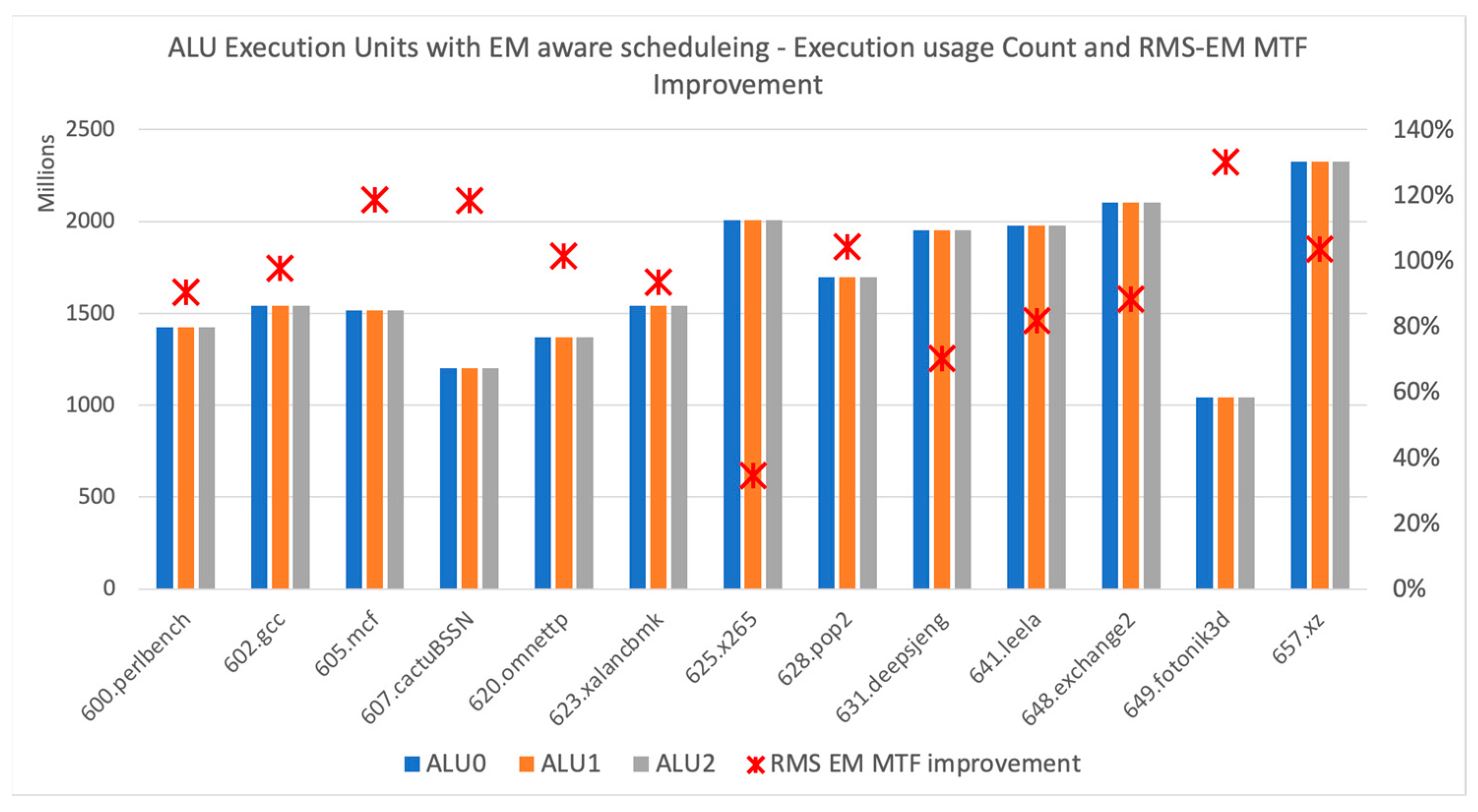
This section examines switching probability hotspots that may accelerate RMS-EM in two different parts of processor microarchitecture: ALU execution units and architecture register files. Previous studies such as [17] support the idea that these areas involve the most intensive EM activities when running such workloads and, thus, will experience intense EM hotspots. Through our experimental analysis we assume a fixed memory hierarchy configuration. The impact of RMS-EM on different memory system hierarchy configurations has been studied by [34,35].

3.2.1. ALUs

Figure 1 illustrates the distribution of processing operations among different ALUs when using the first-in, first-out (FIFO) selection mechanism for the ready-to-execute instructions. Note that ALU0 is the most utilized ALU of the three and ALU2 is the least employed, which is attributed to the fixed allocation policy of the available ALUs; a higher priority is given to an ALU with a lower index. Because ALU execution time is 1 clock cycle, all ALUs become available every cycle. Therefore, when one instruction is issued only ALU0 is allocated. In turn, for two instructions ALU0 and ALU1 are utilized, and when three instructions are issued, all ALUs are employed. Figure 1 shows that ALU0 is used at more than twice the rate as ALU1 and nearly 10 times the rate as ALU2 for most benchmarks. In such a scheduling implementation, ALU0′s worst-case switching factor dictates that the worst-case RMS-EM scenario be applied to all ALUs. Figure 1 also shows the ratio of the average number of ALU allocations to the maximum number (3). In most of the benchmarks, the measured ratio is approximately 50%, which is another indication of the major difference between the maximum number of ALUs utilized and the average number of allocations.

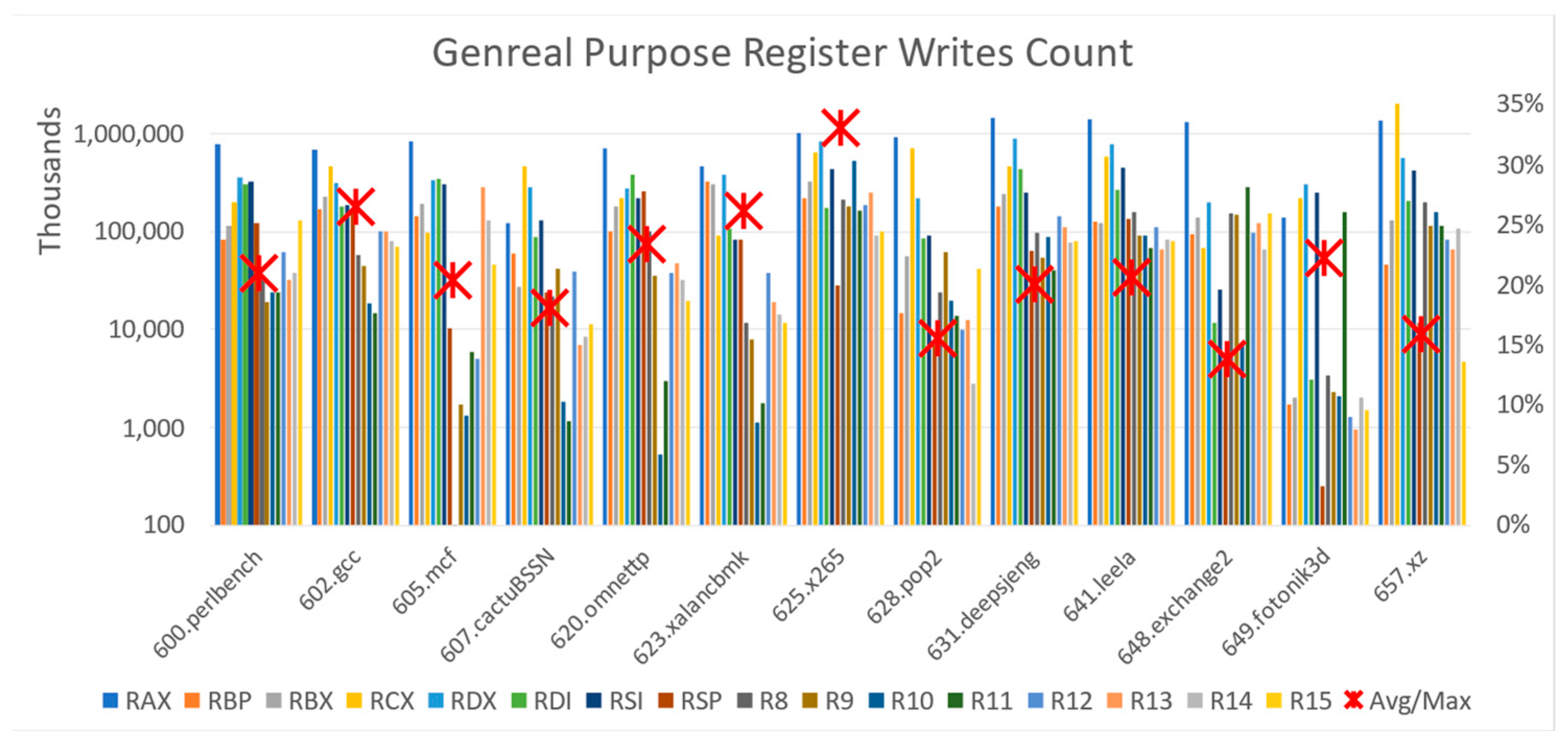
3.2.2. Register File

Our next set of experiments examines the switching factor in architectural registers. Figure 2 illustrates the distribution of write operations on integer general-purpose registers (GPRs) for the Spec2017 benchmarks. The distribution clearly is not uniform. For example, the RAX register is the most-toggled register in terms of write operations, whereas the nonlegacy registers are hardly used and thus are significantly less toggled than the x86 legacy registers. The root cause of these differences is the nature of compiler register-allocation algorithms. Figure 2 also shows that the ratio of the average number of write operations to the maximum number of write operations varies from nearly 7% to 33%. This measurement is another indication that the toggle rate is not equally balanced between registers, so the register with the greatest number of writes dictates the overall switching ratio for RMS-EM.
Figure 3 presents the number of write operations on floating-point (FP) registers for the Spec2017 benchmarks that involve FP operations. The results presented for this case are similar to the results presented in Figure 2. For FP registers, the number of writes is significantly greater in the registers with lower indexes (i.e., the ZMM0, ZMM1, and ZMM2 registers have the highest write count). Similar to integer registers, this can also be explained by the nature of the register-allocation algorithm of common compilers. In this case, the ratio of the average number of write operations to the maximum number of write operations is even smaller, which is indicative of an even larger variance relative to integer registers.

4. Microarchitectures for RMS-EM Avoidance

This section introduces our microarchitecture solutions to eliminate switching probability hotspots and thereby relax RMS-EM sign-off conditions. This approach results in a dramatic relaxation of the overall RMS-EM sign-off design conditions. The principle of our proposed solutions is similar to those employed in the area of workload balancing in computer systems. The idea is based on a switching probability-aware resource allocation scheme that uniformly smooths the utilization of the available computational resources, significantly reducing RMS-EM reliability impact. The following subsections introduce RMS-EM-aware architectures for dealing with RMS-EM switching probability-related hotspots on ALU execution units and register files. The novelty of the proposed solutions may be summarized as follows:
  • We offer RMS-EM-aware architectural solutions dedicated to fundamental microprocessor building elements: register files and execution units, whereas prior studies made limited use of such information.
  • The proposed solutions can be implemented in conjunction with physical-design-based flows and provide a complementary enhancement to such flows.
  • We avoid the need to duplicate logic, reduce performance, or employ dedicated mechanisms to detect EM degradation through normal IC operation that were suggested by [16].
  • The proposed solution eliminates the dynamic power overhead and the design complexity suggested by past studies such as [19].
  • Finally, we avoid compromising reliability and management, as suggested by [12,28].
As part of introducing the principles of our solutions, we also summarize the limitations of the proposed techniques:
  • Our study is limited to digital circuits. Analog circuits are outside the scope of this study.
  • Our solutions are highly effective when the switching probability is a dominant factor in inducing RMS-EM. The proposed techniques may offer a limited benefit for a system with a low activity rate.
  • Our solutions rely on a nonuniform distribution of the switching probability that can be exploited to smooth RMS-EM hotspots. When the switching probability is evenly distributed, the effectiveness of our techniques is limited.

4.1. EM-Aware ALU Allocation

In the previous section, we observed that ALUs are not utilized in an RMS-EM-aware manner, which means that the maximum switching probability is dictated by a small, overused subset of ALUs. The proposed RMS-EM-aware scheme assumes that all pending ALU instructions are allocated to a centralized instruction queue, and in each cycle, a scheduler allocates ALUs to execution-ready instructions. Although the proposed scheme is described for ALUs, it can also be applied to any type of execution unit employed by microprocessors.
In this study, we present two alternatives that implement the same basic principle in different ways. The aim of both solutions is to allocate the resources from a different starting point each time. The first simple solution is to have a counter (e.g., 32-bit counter) that is incremented by each clock cycle and wraps around when expired so that the leading resource number to use is calculated as the counter value modulo the number of physical resources. Thus, for our simulated environment, we assume N = 3. When the counter expires, we reset its content and continue with the allocation in the next cycle.
The second solution is illustrated in Algorithm 1; here, we extend each resource with a single bit (Ex_counter) and add a single global bit (Global_counter) for the overall management of the allocation. All counters are initialized to zero. We suggest that the EM-aware allocation algorithm selects execution units with a corresponding counter state that equals the global counter (denoted by the set M). If the number of available execution units that satisfy this condition exceeds the required number of instructions to be issued (k < |M|), then a subset, Q ⊂ M, (based on the required number of instructions to be issued) of those execution units is selected, and all their corresponding counters are switched (between zero and one). Otherwise, the set M of all execution units with their counter state equal to the global counter is selected, and the rest of the execution units needed to satisfy the required instruction to be issued are selected from the set of other pool of ALUs, Q ⊆ U\M (such that |Q| = k–|M|), for which the counter is not equal to the global counter. In this case, only the global counter and the Ex counters, which are equal to the global counter, are incremented.
Table 2 shows an example of the algorithm output for three ALUs.
Algorithm 1
Input: k < N number of execution units to be allocated.
Output: Vector E = (e0, e1, …, en−1), for every 0 ≤ i ≤ n − 1, only if ei = 1 execution unit i to be allocated; otherwise, not allocated.
Initialization: Ex_counter[i] = 0 for every 0 ≤ i ≤ n − 1, Global_counter = 0

     1. M = {0 ≤ i ≤ n − 1 | Ex_counter[i] = Global_counter}
     2. if k < |M| then
     3.  let Q ⊂ M such that |Q| = k
     4.  ei = 1 for every i∈ Q, otherwise ei = 0
     5.  Ex_counter[i]++ for every i ∈ Q
     6. end if
     7. else // k ≥ |M|
     8.  let Q ⊆ U\M such that |Q| = k–|M|
     9.  ei = 1 for every i ∈ Q ∪ M, otherwise ei = 0
     10. Ex_counter[i]++ for every i ∈ Q ∪ M
     11. Global_counter++
     12. end else
     13. return E
The implementation of the first solution is straightforward and may perform well given a large number of execution units. The implementation of the second solution is slightly more complicated, but our implementation trial indicates that it can be done with negligible overhead in terms of logical area and computation time for both the ALU-selection logic and the counter-incrementation logic. Table 3 summarizes power, timing, and area overhead for a 28 nm process. Note that the proposed solution does not affect timing because the counters are updated in parallel to the ALU execution cycle. In addition, we compare the routing resources used by the two options and find that both use negligible routing resources. Option 1 uses 50 nets with a total wire length of 51 µm using M1–M4 metal layers. Option 2 uses 57 nets with a total wire length of 299 µm using M1–M5 metal layers. Note that the total net length of the original design is 21,255 um, and therefore in both options, the wire length overhead is relatively negligible (0.23% and 0.14% for options 1 and 2, respectively).

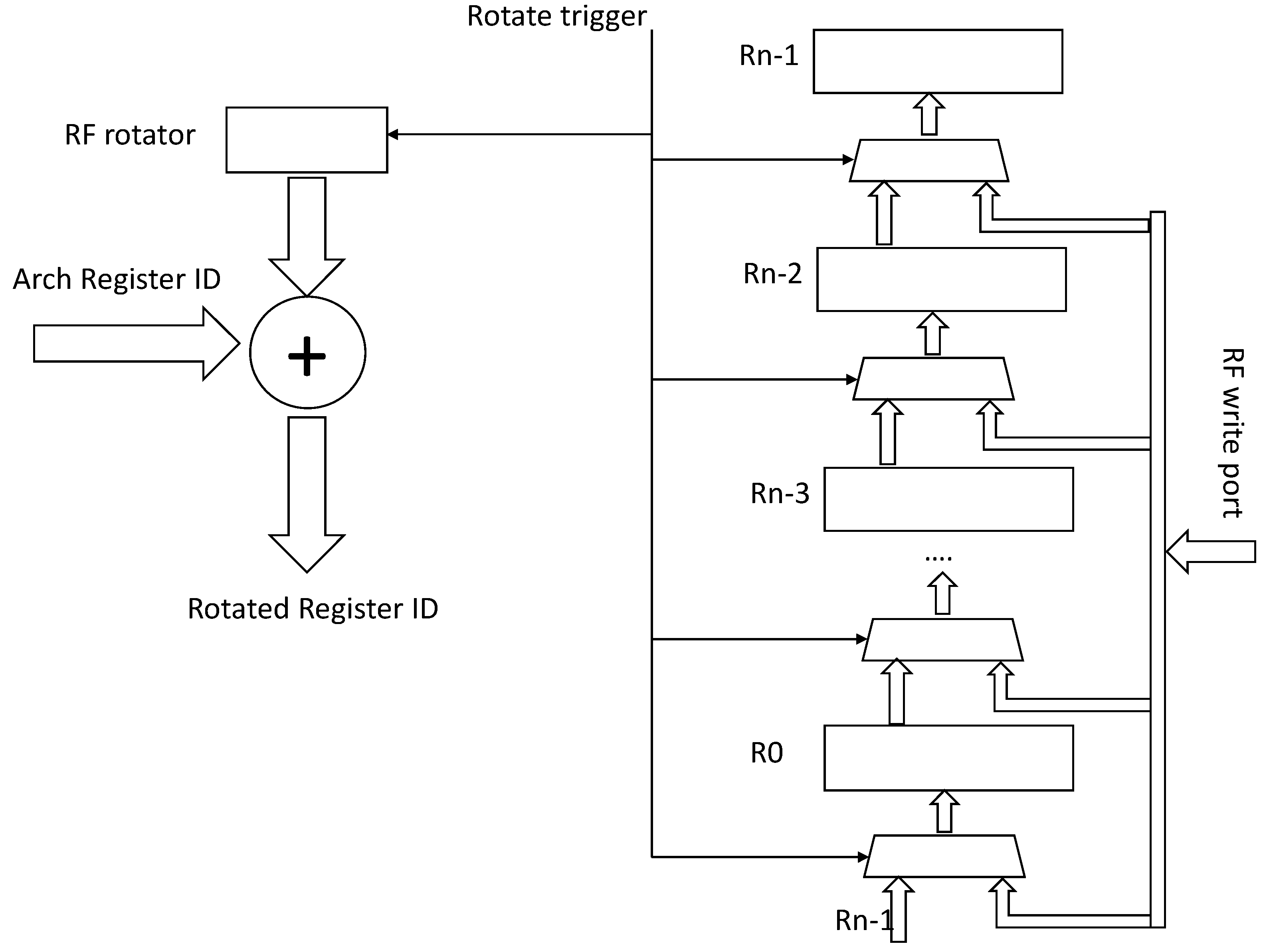
4.2. EM-Aware Register Allocation

The results of the measurements presented in Section 3 clearly indicate that write operations to registers are not uniformly distributed. Moreover, specific registers (e.g., RAX) experienced an excessive number of writes. Such behavior by a small number of registers dictates difficult RMS-EM conditions for all registers and may result in reliability concerns. Note that this section deals mainly with architectural registers assigned by the compiler rather than with physical registers implemented by the out-of-order (OoO) microprocessors. Physical registers are typically implemented as a cyclic buffer within the reorder buffer, and as a result, all writes are spread uniformly over time.
The proposed architectural solution, illustrated in Figure 4, avoids write hotspots in registers by periodically changing the mapping of registers to their corresponding architectural hosting locations. The scheme is based on modulo rotation of the mapping between the architectural register identifier and its physical locations. As illustrated in Figure 4, a pulse trigger is asserted to shift the register mapping in the register file (RF) either periodically (or each time we change CR3) or as part of the return-from-interrupt procedure before saving the values of the user-level process. A modulo counter (RF rotator) serves to map the architectural register number to the physical register location. The physical location of each architectural register is determined by summing the architectural register identifier with the RF rotator value. In addition, two-to-one multiplexors are inserted between adjacent registers to select between the functional RF write-port and the value in the adjacent register (which is selected by a trigger assertion). After each assertion of the rotation trigger (at any arbitrary time point), the counter is incremented, and the physical register values are shifted between neighboring registers by changing the control of the multiplexors and asserting the load-enable control signal of the registers.
Table 4 summarizes power, timing path, and area overhead for a 28 nm process (for 32 GPRs):

5. Experimental Analysis of RMS-EM-Aware Architecture

This section presents the experimental results for the proposed architecture solutions (presented in the previous section) to reduce the impact of RMS-EM. The metric of MTF improvement is defined as the increase in the RMS-EM-aware MTF with respect to the original MTF. It is obtained by applying Equation (4):
MTF   improvement = MTF RMS   EM aware MTF original 1 = p max   original p max   RMS   EM aware 1 ,
where pmax RMS EM-aware and pmax original are the maximum toggle rates of a module with an RMS-EM-aware architecture and the original architecture, respectively.
Because the techniques we proposed in Section 4 did not report performance overhead, this section focuses on how the proposed algorithms affect the MTF improvement. Our experimental analysis starts by examining the improvement of RMS-EM MTF provided by the proposed solution by relaxing the maximum switching probability. Next, we validate our experimental observation via extensive physical RMS-EM simulations that consider the Joule heating effect through dynamic high-resolution thermal analyses.

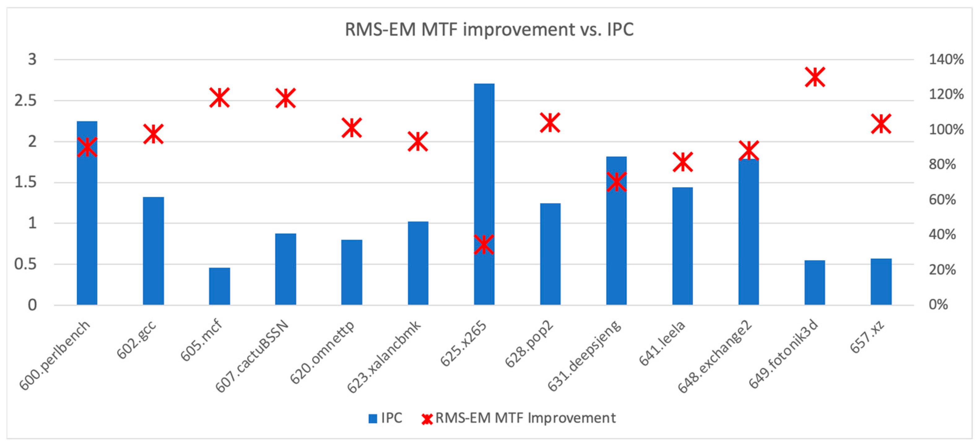
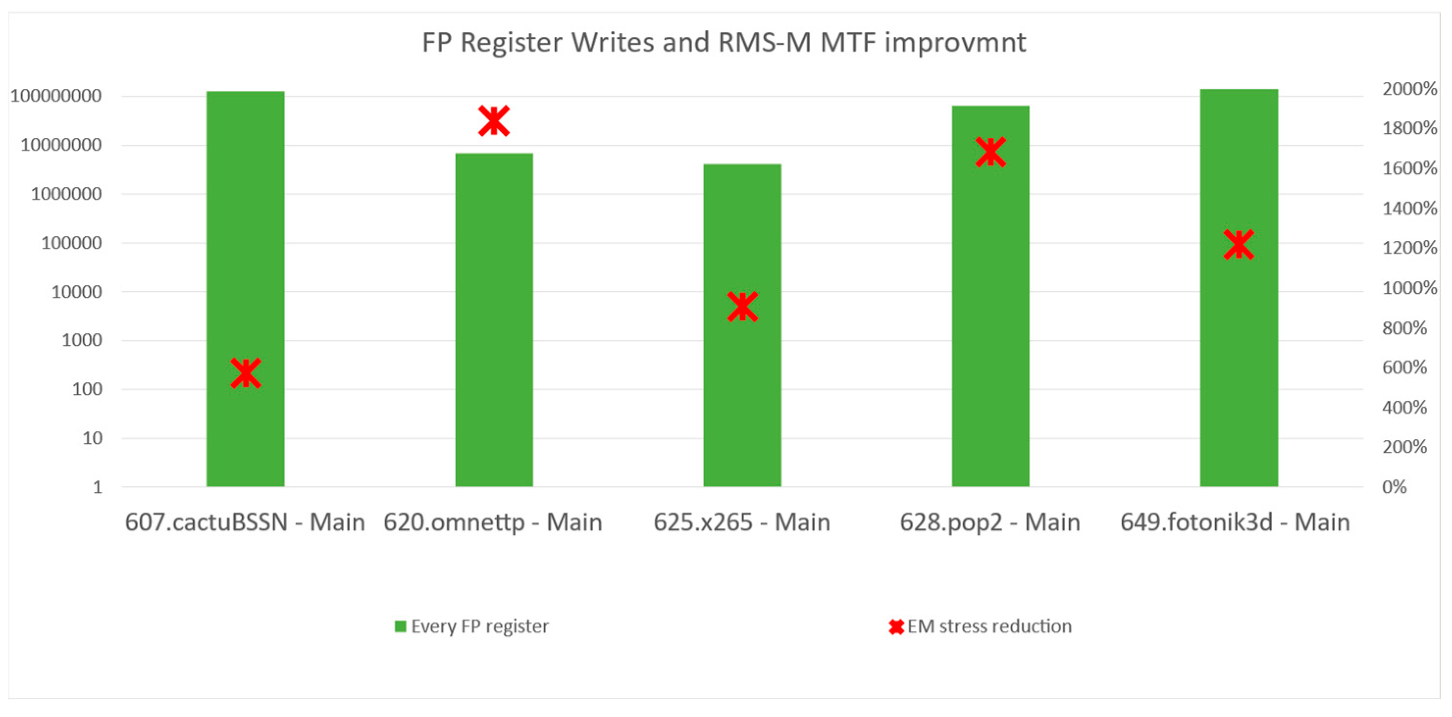
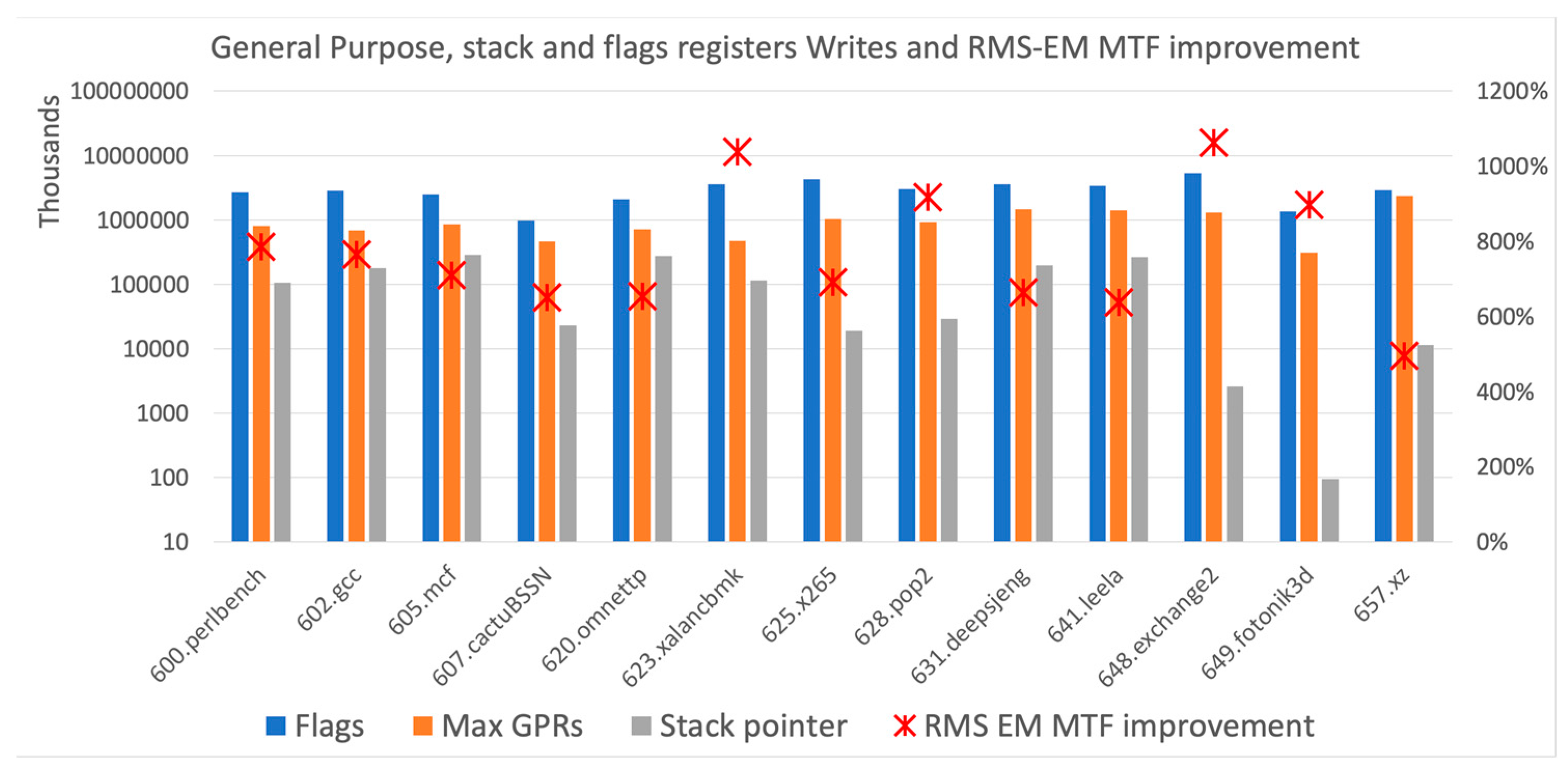
5.1. Toggle Rate-Based Experimental Analysis for RMS-EM MTF Improvement

We first examine an RMS EM-aware solution for ALU execution units. Figure 5 shows how the solution described in Algorithm 1 affects the RMS-EM MTF for the SPEC2017 benchmarks. An examination of the two solutions introduced in the last section indicates that they behave similarly. The results show that the proposed algorithm efficiently eliminates ALU usage hotspots and can potentially improve RMS-EM MTF by approximately 100% on average. The results vary from nearly 34% potential MTF improvement up to a 130% improvement. This result is because the proposed scheme distributes ALU use uniformly and reduces the RMS-EM hotspots.
As part of this study, we also compare the instructions per cycle (IPC) versus the potential RMS-EM MTF improvement, as shown in Figure 6. Benchmarks with a small IPC have a greater potential for RMS-EM MTF improvement because of the underused ALUs that could potentially help reduce the maximum RMS-EM hotspots.
The next results show the potential RMS-EM MTF improvement obtained by the proposed architectural solution for the GPR and FP register files (Figure 7 and Figure 8, respectively). For both register files, the number of writes is distributed uniformly over all registers, and no hotspots exist (every bar in the graph represents an equal number of writes per every register). In addition, the MTF potentially improves by nearly 400% on average for the GPRs and 1200% on average for the FP registers. The rotation trigger in the simulation was asserted every 10 million clock cycles. We examined different rotation trigger rates and found that this value does not impact performance.
As part of the experiments, we also observed that the flags and stack-pointer registers experienced excessive stress during write operations, which makes them highly susceptible to RMS-EM. Figure 9 illustrates the number of write operations to the flag and stack-pointer registers and compares them with the maximum number of writes per register in the GPR register file. For almost all benchmarks, the number of writes to the flag register significantly exceeds those to the GPR and stack-pointer registers. This is because almost every instruction involves implicit writes to the flag register, which motivated us to extend the EM-aware scheme proposed for the GPR register file to include the flag and stack-pointer registers. Figure 9 shows that, in this case, the maximum number of write operations is reduced even more (between 80% and 90%) and that the potential MTF improvement is more than 760% on average.
Based on the experimental results, we observe that RMS-EM MTF can be significantly extended in the microprocessors’ building blocks that are examined. Our observations reveal an average improvement in RMS-EM MTF by 100% for ALUs, 400% for the integer register files, and 1200% for FP register files. These results indicate that the proposed EM-aware solution should allow microprocessor designers to significantly relax the maximum switching probability and, as a result, avoid a significant number of potential RMS-EM violations.
Alternatively, the reduction in the maximum switching rate translates into an extended device lifetime. Because the RMS-EM MTF and device lifetime depend on both the switching probability and the electrical and thermal characteristics of the circuit, we extend our experimental analysis by performing physical simulations that consider the Joule heating effect and toggle rate.

5.2. Physical RMS-EM Simulations Based on Joule Heating Effect

In the last part of our experimental analysis, we present extensive physical simulations that consider both the toggle rate and the Joule heating effect through a dynamic, high-resolution thermal analysis. The simulations were implemented in the Cadence® VoltusTM simulation environment [36], which performs detailed RMS-EM analysis of the Joule heating effect and self-heating under different toggle rates. VoltusTM is considered an industry standard for EM sign-off and is certified as an EM sign-off tool by many foundries. The simulation environment takes into account the parameters of transistors that contribute to the RMS current, such as drive strength (fins, number of fingers), channel length, and channel width. The tool makes detailed RMS current calculations to analyze the Joule heating effect and self-heating on all signal wires while taking into account metal dimensions and type. (Power-grid connections are beyond the scope of this analysis.) As part of the simulation process, the tool also certifies that the calculated RMS current of every net does not exceed the maximum RMS current, which is considered a mandatory reliability criterion and is specified in the foundry technology file [25].
The VoltusTM environment requires to synthesize and place-and-route the design under test. The full implementation flow was done on the three architectural structures introduced in Section 4: ALU and register files. The design parameters, implementation tools, and simulation environment are summarized in Table 5. Through the RMS-EM simulations, VoltusTM calculates the RMS current and IRMS, for every metal net in the design while considering the toggle rate obtained from the functional simulations. The technology file, which is provided by the foundry, specifies the maximum allowed RMS current, IRMS_MAX, per metal layer based on its physical properties (physical dimension and material type).
Figure 10 summarizes the reduction of the ratio of IRMS to IRMS_MAX in the design with the EM-aware architecture versus the original design for each benchmark that we used. In addition, it presents the percentage of metal nets that can leverage such RMS current reduction. The results show that, for the ALU, nearly all nets can leverage a reduction of approximately 30% in RMS current, and 55% of the RF nets experience a 68% reduction in their RMS current. Note that the metal nets that do not leverage a reduction in the RMS current already exhibited a small RMS current, so their overall improvement is not noticeable by the tool. The extended MTF as a result of IRMS reduction can be calculated using Equation (3). The extended MTF is proportional to the ratio of IRMS_MAX to the reduced IRMS to the power of two. Thus, the observed RMS current reduction offers at least a x2 and x10 lifetime extension for ALUs and register files, respectively. One may note that the extended MTF experimental results that are obtained using the RMS-EM physical simulation are similar to the MTF improvement prediction provided by the experimental results in Figure 5, Figure 7, Figure 8 and Figure 9, which were based on the switching probability reduction.

6. Conclusions

Microprocessor reliability is a crucial requirement that introduces major microarchitectural and design challenges. Traditionally, reliability and RMS-EM-related issues are handled at the physical design level, which enforces design rules using worst-case scenario analysis to detect violations and attempt to solve them. In our study, we presented an RMS-EM-aware microarchitectural solution that can significantly relax the overdesign of traditional methods and significantly extend a microprocessor’s lifetime.
This paper indicates that microprocessors are highly susceptible to RMS-EM because they process highly variable dynamic workloads on non-EM-aware microarchitectures. Thus, we proposed architectural solutions that take into account the RMS-EM effect and reduce excess use of execution units and write operations to registers. The principle of the proposed solutions is based on RMS-EM-aware resource allocation that attempts to uniformly distribute write operations and the use of computational elements over all available resources. This solution can be incorporated into physical-design-based approaches where it offers a complementary enhancement to existing methods. Our analysis shows that the proposed solutions incur minor area and power overhead and negligible performance degradation with respect to prior studies. In addition, our experimental results indicate that the proposed architecture significantly relaxes the RMS-EM switching probability sign-off conditions by 50% for ALUs and 80–90% for the register files. Our RMS- EM physical simulations indicate that such toggle rate relaxation leads to a dramatic reduction in IRMS: 30% and 68% for ALUs and register files, respectively. Using Equation (3) for the IRMS produces a lifetime extension of approximately 2x and 10x for ALUs and register files, respectively.
EM has become a major challenge in advanced technologies, and further studies are required to continue exploring new architectures and identify other avenues to reduce EM and extend device lifetime. In this study, we examined how RMS-EM affects modern microprocessors, although the approach we describe here may be extended to other processing elements such as security engines, memory system hierarchy, GPUs, and TPUs. We also encourage future studies to examine software-based solutions for RMS-EM reduction.

Author Contributions

Conceptualization, F.G. and A.M.; methodology, F.G.; software, F.G.; validation, F.G., and A.M.; formal analysis, F.G.; investigation, F.G.; resources, F.G.; data curation, F.G.; writing—original draft preparation, F.G.; writing—review and editing, F.G. and A.M.; visualization, F.G.; supervision, F.G. and A.M.; project administration, F.G. All authors have read and agreed to the published version of the manuscript.

Funding

This research received no external funding.

Data Availability Statement

Not applicable.

Conflicts of Interest

The authors declare no conflict of interest.

References

  1. Tan, S.X.-D.; Tahoori, M.; Kim, T.; Wang, S.; Sun, Z.; Kiamehr, S. Long-Term Reliability of Nanometer VLSI Systems—Modeling, Simulation and Optimization; Springer Publisher: Berlin/Heidelberg, Germany, 2019; ISBN 978-3-030-26171-9. [Google Scholar] [CrossRef]
  2. Lienig, J.; Jerke, G. Embedded Tutorial: Electromigration-Aware Physical Design of Integrated Circuits. In Proceedings of the 18th International Conference on VLSI Design held jointly with 4th International Conference on Embedded Systems Design, Kolkata, India, 3–7 January 2005; IEEE Press: Piscataway, NJ, USA, 2005; pp. 77–82. [Google Scholar]
  3. Lienig, J. Introduction to electromigration-aware physical design. In Proceedings of the International Symposium on Physical Design (ISPD’06), San Jose, CA, USA, 9–12 April 2006; ACM: New York, NY, USA, 2006; pp. 39–46. [Google Scholar]
  4. Huang, X.; Kteyan, A.; Tan, S.X.-D.; Sukharev, V. Physics-Based Electromigration Models and Full-Chip Assessment for Power Grid Networks. IEEE Trans. Comput.-Aided Des. Integr. Circuits Syst. 2016, 35, 1848–1861. [Google Scholar] [CrossRef]
  5. Sun, Z.; Yu, S.; Zhou, H.; Liu, Y.; Tan, S.X.-D. EMSpice: Physics-Based Electromigration Check Using Coupled Electronic and Stress Simulation. IEEE Trans. Device Mater. Reliab. 2020, 20, 376–389. [Google Scholar] [CrossRef]
  6. Najm, F.N.; Sukharev, V. Efficient Simulation of Electromigration Damage in Large Chip Power Grids Using Accurate Physical Models (Invited Paper). In Proceedings of the 2019 IEEE International Reliability Physics Symposium (IRPS), Monterey, CA, USA, 31 March–4 April 2019; pp. 1–10. [Google Scholar] [CrossRef]
  7. Chatterjee, S.; Sukharev, V.; Najm, F.N. Power Grid Electromigration Checking Using Physics-Based Models. IEEE Trans. Comput.-Aided Des. Integr. Circuits Syst. 2018, 37, 1317–1330. [Google Scholar] [CrossRef]
  8. Maiz, J.A. Characterization of electromigration under bidirectional (BC) and pulsed unidirectional (PDC) currents. In Proceedings of the International Reliability Physics Symposium (IRPS), Phoenix, AZ, USA, 11–13 April 1989; pp. 220–228. [Google Scholar]
  9. Jonggook, K.; Tyree, V.C.; Crowell, C.R. Temperature gradient effects in electromigration using an extended transition probability model and temperature gradient free tests. In I. Transition probability model. In Proceedings of the IEEE International Integrated Reliability Workshop Final Report, Lake Tahoe, CA, USA, 18–21 October 1999; pp. 24–40. [Google Scholar] [CrossRef]
  10. Yu, X.; Weide, K. A study of the thermal-electrical- and mechanical influence on degradation in an aluminum-pad structure. Microelectron. Reliab. 1997, 37, 1545–1548. [Google Scholar] [CrossRef]
  11. Lienig, J. Electromigration and Its Impact on Physical Design in Future Technologies. In Proceedings of the 2013 ACM International Symposium on Physical Design, Stateline, NV, USA, 24–27 March 2013. [Google Scholar]
  12. Srinivasan, J.; Adve, S.V.; Bose, P.; Rivers, J.A. Lifetime Reliability: Toward an Architectural Solution. IEEE Micro 2005, 25, 70–80. [Google Scholar] [CrossRef]
  13. Srinivasan, J.; Adve, S.V.; Bose, P.; Rivers, J.A. Exploiting Structural Duplication for Lifetime Reliability Enhancement. In Proceedings of the 32nd International Symposium on Computer Architecture, Madison, WI, USA, 4–8 June 2005. [Google Scholar]
  14. Dasgupta, A.; Karri, R. Electromigration Reliability Enhancement Via Bus Activity Distribution. In Proceedings of the 33rd Annual Conference Design Automation (DAC 96), Las Vegas, NV, USA, 3–7 June 1996; ACM Press: New York, NY, USA, 1996; pp. 353–356. [Google Scholar]
  15. Abella, J.; Vera, X.; Ergin, S.U.O.; González, A.; Tschanz, J.W. Refueling: Preventing Wire Degradation due to Electromigration. IEEE Micro 2008, 28, 37–46. [Google Scholar] [CrossRef] [Green Version]
  16. Tao, J.; Chen, J.; Cheung, N.; Hu, C. Modeling and characterization of electromigration failures under bidirectional current stress. IEEE Trans. Electron Devices 1996, 43, 800–808. [Google Scholar]
  17. Abella, J.; Vera, X. Electromigration for Microarchitects. ACM Comput. Surv. 2010, 42, 9. [Google Scholar] [CrossRef]
  18. Gabbay, F.; Mendelson, A. Electromigration-Aware Instruction Execution for Modern Microprocessors. In Proceedings of the 2022 the 4th International Conference on Microelectronic Device and Technologies (MicDAT ‘2022), Corfu, Greece, 21–23 September 2022; pp. 60–66, ISBN 978-84-09-43856-3. [Google Scholar]
  19. Operating Temperature. Wikipedia. Available online: https://en.wikipedia.org/wiki/Operating_temperature (accessed on 8 January 2023).
  20. AEC-Q100-REV-G Standard; Failure Mechanism based Stress test Qualification for Integrated Circuit. Automotive Electronics Council, Component Technical Committee: Devon UK, 2014.
  21. Black, J.R. Electromigration—A brief survey and some recent results. IEEE Trans. Electron. Devices 1969, 16, 338–347. [Google Scholar] [CrossRef] [Green Version]
  22. Kahng, A.B.; Nath, S.; Rosing, T.S. On Potential Design Impacts of Electromigration Awareness. In Proceedings of the 2013 18th Asia and South Pacific Design Automation Conference (ASP-DAC), Yokohama, Japan, 22–25 January 2013. [Google Scholar]
  23. LEF DEF Reference. Available online: https://www.ispd.cc/contests/18/lefdefref.pdf (accessed on 8 January 2023).
  24. Scorzoni, A.; Neri, B.; Caprile, C.; Fantini, F. Electromigration in thin- film inter-connection lines: Models, methods and results. Mater. Sci. Rep. 1991, 7, 143–219. [Google Scholar] [CrossRef]
  25. Valero, A.; Miralaei, N.; Petit, S.; Sahuquillo, J.; Jones, T.M. On Microarchitectural Mechanisms for Cache Wearout Reduction. IEEE Trans. Very Large-Scale Integr. (VLSI) Syst. 2017, 25, 857–871. [Google Scholar] [CrossRef] [Green Version]
  26. Hau-Riege, C.S. An introduction to Cu electromigration. Microel. Reliab. 2004, 44, 195–205. [Google Scholar] [CrossRef]
  27. Wang, S.; Kim, T.; Sun, Z.; Tan, S.X.-D.; Tahoori, M. Recovery-aware proactive TSV repair for electromigration lifetime enhancement in 3D ICs. IEEE Trans. Very Large Scale Integr. Syst. 2018, 26, 531–543. [Google Scholar] [CrossRef]
  28. Srinivasan, J.; Adve, S.V.; Bose, P.; Rivers, J.A. The Case for Lifetime Reliability-Aware Microprocessors. In Proceedings of the 31st International Symposium on Computer Architecture (ISCA ’04), München, Germany, 19–23 June 2004. [Google Scholar]
  29. Swaminathan, K.; Chandramoorthy, N.; Cher, C.; Bertran, R.; Buyuktosunoglu, A.; Bose, P. BRAVO: Balanced Reliability-Aware Voltage Optimization. In Proceedings of the 2017 IEEE International Symposium on High Performance Computer Architecture (HPCA), Austin, TX, USA, 4–8 February 2017; pp. 97–108. [Google Scholar] [CrossRef]
  30. Carlson, T.E.; Heirman, W.; Eeckhout, L. Sniper: Exploring the level of abstraction for scalable and accurate parallel multi-core simulations. In Proceedings of the International Conference for High Performance Computing, Net- working, Storage and Analysis (SC), Seattle, WA, USA, 12–18 November 2011. [Google Scholar]
  31. Thomadakis, M.E. The Architecture of the Nehalem Processor and Nehalem-EP SMP Platforms. Technical Report, December 2010. Available online: https://d1wqtxts1xzle7.cloudfront.net/30311675/nehalem-libre.pdf?1390883858=&response-content-disposition=inline%3B+filename%3DThe_architecture_of_the_Nehalem_processo.pdf&Expires=1673405927&Signature=ZzDFsTSVLljHcDVxkE-D8ky1A7gj51jo2qCHxmcK-Wcje6wwP6RNXd8jRVXTMb4zXytw3S-cO8XecXMUWrqeuuHgUrTtuP0hX3C8x47NNq6cXwsxNb6M~lvk7O1BFLxeDszoMkAKWi45u~RQ7U69XkAzZHck-009CbGkkACtUTDL-zAJrnM6IvN4I7pot4UdL~yRPmi6pmP2hlMTIulNXQgI3ICUDSH9zv4qwTnA~GXrMND3LMKlTEIH4n4LFjfR9gT-U7ShkuKwX-cy8GRyVhX0hyjdWUwwnZ52A-o4UqSmnA5emOHrHZAEXO8D~fk0SxW24DivfwlOL-NWSMCQpQ__&Key-Pair-Id=APKAJLOHF5GGSLRBV4ZA (accessed on 8 January 2023).
  32. Limaye, A.; Adegbija, T. A workload characterization of the spec cpu2017 benchmark suite. In Proceedings of the 2018 IEEE International Symposium on Performance Analysis of Systems and Software (ISPASS), Belfast, UK, 2–4 April 2018; pp. 149–158. [Google Scholar]
  33. Wu, Q.; Flolid, S.; Song, S.; Deng, J.; John, L.K. Hot Regions in SPEC CPU2017. In Proceedings of the 2018 IEEE International Symposium on Workload Characterization (IISWC), Raleigh, NC, USA, 30 September–2 October 2018. [Google Scholar]
  34. Zhang, R.; Liu, T.; Yang, K.; Milor, L. CacheEM: For Reliability Analysis on Cache Memory Aging Due to Electromigration. IEEE Trans. Comput.-Aided Des. Integr. Circuits Syst. 2022, 41, 3078–3091. [Google Scholar] [CrossRef]
  35. Zhang, R.; Yang, K.; Liu, T.; Milor, L. Modeling of FinFET SRAM array reliability degradation due to electromigration. Microelectron. Reliab. 2019, 100–101, 113485. [Google Scholar] [CrossRef]
  36. VoltusTM User Guide. Available online: http://www.cadence.com (accessed on 8 January 2023).
Figure 1. Distribution of ALU execution count.
Jlpea 13 00007 g001
Figure 2. Distribution of general-purpose register writes.
Jlpea 13 00007 g002
Figure 3. Distribution of writes to floating-point registers.
Jlpea 13 00007 g003
Figure 4. Scheme for EM-aware RF mapping.
Jlpea 13 00007 g004
Figure 5. Distribution of ALU execution usage count and MTF improvement with RMS EM-aware allocation.
Jlpea 13 00007 g005
Figure 6. ALU EM stress reduction versus IPC.
Jlpea 13 00007 g006
Figure 7. GPR writes distribution with RMS-EM MTF improvement.
Jlpea 13 00007 g007
Figure 8. FP register writes distribution with RMS-EM MTF improvement.
Jlpea 13 00007 g008
Figure 9. Distribution of GPRs, flag, and stack pointer writes with EM-aware allocation.
Jlpea 13 00007 g009
Figure 10. Physical RMS-EM simulations: IRMS/IRMS-Max ratio reduction of the EM-aware architecture with respect to the original design measurements.
Jlpea 13 00007 g010
Table 1. Baseline simulation model configuration.
Core Model
Frequency2.66 GHz
Execution units [time]3 ALUs [1 cycle]
1 FP add/sub [3 cycles]
1 FP mul/div [5/6 cycles]
1 Branch [1 cycle]
1 Load unit [1 cycle]
1 Store unit [1 cycle]
PipelineDispatch width: 4
Instruction window128
Memory system model
Block size64 bytes
L1-D cache32 KB, 8-way
L1-I cache32 KB, 4-way
L2 cache256 KB, 8-way
L3 cache8 MB, 16-way
DTLB64 entries, 4-way
ITLB128 entries, 4-way
STLB 512 entries, 4-way (secondary TLB)
Table 2. Example of EM-aware ALU scheduling.
Clock CycleIssued
Instructions
Ex_counter [2:0]Global CounterSelected ALU(s)
000, 0, 00None
120, 1, 100, 1
221, 1, 012, 0
330, 0, 101, 2, 0
Table 3. ALU EM-Aware scheduling overhead.
OptionOriginal Area [um2]Area Overhead
[um2]/[%]
Original Power
[uW]
Power Overhead
[uW]/[%]
Timing
Impact
1200,613316/0.15641.790.031/0.004%None (reg-to-reg delay < clock cycle time)
2200,61385.9/0.04641.790.026/0.004%None (reg-to-reg delay < clock cycle time)
Table 4. GPR rotation overhead.
Original Area [um2]Area Overhead
[um2]/[%]
Original Power
[uW]
Power
[uW] /[%]
Timing Impact
77,2341973 / 2.520,1620.282/0.00150 ps delay added to access time
Table 5. Implementation and RMS-EM simulation tools and design parameters.
Physical Simulation Environment Parameters
Synthesis toolCadence® GenusTM version 19.11-s087_1
Place-and-route toolCadence® InnovusTM version 19.11-s128_1
EM toolCadence® VoltusTM version 19.11-s129_1
Process28 nm
Clock frequency2.66 GHz
Core voltage0.9 V
Tj105 °C (self-heating is modeled by the VoltusTM simulation environment)
Metal layersMetal 1 to metal 9
Disclaimer/Publisher’s Note: The statements, opinions and data contained in all publications are solely those of the individual author(s) and contributor(s) and not of MDPI and/or the editor(s). MDPI and/or the editor(s) disclaim responsibility for any injury to people or property resulting from any ideas, methods, instructions or products referred to in the content.

