
First-Principles Investigation of Electronic and Related Properties of Cubic Magnesium Silicide (Mg2Si)
 , ,
, ,
Abstract
:1. Introduction and Motivation
2. Computational Method
3. Results
4. Discussion
5. Conclusions
Author Contributions
Funding
Data Availability Statement
Conflicts of Interest
References
- Scouler, W.J. Optical Properties of Mg2Si, Mg2Ge, and Mg2Sn from 0.6 to 11.0 eV at 77 °K. Phys. Rev. 1969, 178, 1353–1357. [Google Scholar] [CrossRef]
- Borisenko, V.E. Semi-conducting Silicides. Springer Series in Material Science; Springer: New York, NY, USA, 2000. [Google Scholar] [CrossRef]
- Morris, R.G.; Redin, R.D.; Danielson, G.C. Semiconducting Properties ofMg2Si Single Crystals. Phys. Rev. 1957, 1957, 1909–1915. [Google Scholar] [CrossRef]
- Zaitsev, V.K.; Fedorov, M.I.; Gurieva, E.A.; Eremin, I.S.; Konstantinov, P.P.; Samunin, A.Y.; Vedernikov, M.V. Highly effectiveMg2Si1−xSnxthermoelectrics. Phys. Rev. B 2006, 74, 045207. [Google Scholar] [CrossRef]
- Stella, A.; Brothers, A.D.; Hopkins, R.H.; Lynch, D.W. Pressure Coefficient of the Band Gap in Mg2Si, Mg2Ge, and Mg2Sn. Phys. Status Solidi (b) 1967, 23, 697–702. [Google Scholar] [CrossRef]
- Satyala, N.; Vashaee, D. Modeling of Thermoelectric Properties of Magnesium Silicide (Mg2Si). J. Electron. Mater. 2012, 41, 1785–1791. [Google Scholar] [CrossRef]
- Kato, T.; Sago, Y.; Fujiwara, H. Optoelectronic properties of Mg2Si semiconducting layers with high absorption coefficients. J. Appl. Phys. 2011, 110, 063723. [Google Scholar] [CrossRef]
- Buchenauer, C.J.; Cardona, M. Raman Scattering in Mg2Si, Mg2Ge, and Mg2Sn. Phys. Rev. B 1971, 3, 2504–2507. [Google Scholar] [CrossRef]
- Vazquez, F.; Forman, R.A.; Cardona, M. Electroreflectance Measurements on Mg2Si, Mg2Ge, and Mg2Sn. Phys. Rev. 1968, 176, 905–908. [Google Scholar] [CrossRef]
- Sobolev, V.V. Reflectivity spectra and energy band structure of Mg2X crystals. Phys. Status Solidi (b) 1972, 209, K209–K214. [Google Scholar] [CrossRef]
- Tejeda, J.; Cardona, M. Valence bands of theMg2X (X = Si, Ge, Sn ssemiconducting compounds. Phys. Rev. B 1976, 14, 2559–2568. [Google Scholar] [CrossRef]
- McWilliams, D.; Lynch, D.W. Infrared Reflectivities of Magnesium Silicide, Germanide, and Stannide. Phys. Rev. 1963, 130, 2248–2252. [Google Scholar] [CrossRef]
- Panke, D.; Wölfel, E. Die Verteilung der Valenzelektronen im Mg2Si. Z. Für Krist.-Cryst. Mater. 1969, 129, 28. [Google Scholar] [CrossRef]
- Heller, M.; Danielson, G. Seebeck effect in Mg2Si single crystals. J. Phys. Chem. Solids 1962, 23, 601–610. [Google Scholar] [CrossRef]
- Busch, G.; Winkler, U. Elektrische Eigenschaften Der Intermetallischen Verbindungen Mg2Si, Mg2Ge, Mg2Sn Und Mg2Pb. Physica 1954, 20, 1067–1072. [Google Scholar] [CrossRef]
- Koenig, P.; Lynch, D.W.; Danielson, G.C. Infrared absorption in magnesium silicide and magnesium germanide. J. Phys. Chem. Solids 1961, 20, 122–126. [Google Scholar] [CrossRef] [Green Version]
- Pandit, P.; Sanyal, S.P. First principles study of electronic, elastic and lattice dynamical properties of Mg2X (X = Si, Ge and Sn) compounds. Indian J. Pure Appl. Phys. 2011, 49, 692–697. [Google Scholar]
- Corkill, J.L.; Cohen, M.L. Structural, bonding, and electronic properties of IIA-IV antifluorite compounds. Phys. Rev. B 1993, 48, 17138–17144. [Google Scholar] [CrossRef]
- Boulet, P.; Verstraete, M.; Crocombette, J.-P.; Briki, M.; Record, M.-C. Electronic properties of the Mg2Si thermoelectric material investigated by linear-response density-functional theory. Comput. Mater. Sci. 2011, 50, 847–851. [Google Scholar] [CrossRef] [Green Version]
- Imai, Y.; Watanabe, A.; Mukaida, M. Electronic structures of semiconducting alkaline-earth metal silicides. J. Alloy. Compd. 2003, 358, 257–263. [Google Scholar] [CrossRef]
- Arnaud, B.; Alouani, M. Electron-hole excitations inMg2SiandMg2Gecompounds. Phys. Rev. B 2001, 64, 0332021–0332024. [Google Scholar] [CrossRef]
- Mars, K.; Ihou-Mouko, H.; Pont, G.; Tobola, J.; Scherrer, H. Thermoelectric Properties and Electronic Structure of Bi- and Ag-Doped Mg2Si1−x Ge x Compounds. J. Electron. Mater. 2009, 38, 1360–1364. [Google Scholar] [CrossRef]
- Au-Yang, M.Y.; Cohen, M.L. Electronic Structure and Optical Properties of Mg2Si, Mg2Ge, and Mg2Sn. Phys. Rev. 1969, 178, 1358–1364. [Google Scholar] [CrossRef]
- Aymerich, F.; Mula, G. Pseudopotential band structures of Mg2Si, Mg2Ge, Mg2Sn, and of the solid solution Mg2(Ge, Sn). Phys. Status Solidi (b) 1970, 42, 697–704. [Google Scholar] [CrossRef]
- Balout, H.; Boulet, P.; Record, M.-C. Electronic and transport properties of Mg2Si under isotropic strains. Intermetallics 2014, 50, 8–13. [Google Scholar] [CrossRef]
- Krivosheeva, A.V.; Kholod, A.N.; Shaposhnikov, V.L.; Krivosheev, A.E.; Borisenko, V.E. Band structure of Mg2Si and Mg2Ge semiconducting compounds with a strained crystal lattice. Semiconductors 2002, 36, 496–500. [Google Scholar] [CrossRef]
- Fan, W.H.; Chen, R.X.; De Han, P.; Meng, Q.S. First-Principle Study of Electronic Structures of Y-Doped Mg2Si. Mater. Sci. Forum 2011, 689, 102–107. [Google Scholar]
- Chen, Q.; Xie, Q. First-principles calculations on the electronic structure and optical properties of Mg2Si epitaxial on Si (111). Phys. Procedia 2011, 11, 134–137. [Google Scholar] [CrossRef] [Green Version]
- Ryu, B.; Park, S.; Choi, E.-A.; de Boor, J.; Ziolkowski, P.; Chung, J.; Park, S.D. Hybrid-Functional and Quasi-Particle Calculations of Band Structures of Mg2Si, Mg2Ge, and Mg2Sn. J. Korean Phys. Soc. 2019, 75, 144–152. [Google Scholar] [CrossRef] [Green Version]
- Feibelman, P.J.; Appelbaum, J.A.; Hamann, D.R. Electronic structure of a Ti (0001) film. Phys. Rev. B 1979, 20, 1433–1443. [Google Scholar] [CrossRef]
- Harmon, B.N.; Weber, W.; Hamann, D.R. Total-energy calculations for Si with a first-principles linear-combination-of-atomic-orbitals method. Phys. Rev. B 1982, 25, 1109–1115. [Google Scholar] [CrossRef]
- Franklin, L.; Ekuma, C.; Zhao, G.; Bagayoko, D. Density functional theory description of electronic properties of wurtzite zinc oxide. J. Phys. Chem. Solids 2013, 74, 729–736. [Google Scholar] [CrossRef]
- Bagayoko, D.; Franklin, L.; Zhao, G.L. Predictions of electronic, structural, and elastic properties of cubic InN. J. Appl. Phys. 2004, 96, 4297–4301. [Google Scholar] [CrossRef]
- Bagayoko, D.; Zhao, G.L.; Fan, J.D.; Wang, J.T. Ab initio calculations of the electronic structure and optical properties of ferroelectric tetragonal. J. Phys. Condens. Matter 1998, 10, 5645–5655. [Google Scholar] [CrossRef]
- Ekuma, C.; Franklin, L.; Zhao, G.L.; Wang, J.T.; Bagayoko, D. Local density approximation description of electronic properties of wurtzite cadmium sulfide (w-CdS). Can. J. Phys. 2011, 89, 319–324. [Google Scholar] [CrossRef] [Green Version]
- Ayirizia, B.A.; Malozovsky, Y.; Franklin, L.; Bhandari, U.; Bagayoko, D. Ab-Initio Self-Consistent Density Functional Theory Description of Rock-Salt Magnesium Selenide (MgSe). Mater. Sci. Appl. 2020, 11, 401–414. [Google Scholar] [CrossRef]
- Bagayoko, D. Understanding the Relativistic Generalization of Density Functional Theory (DFT) and Completing It in Practice. J. Mod. Phys. 2016, 07, 911–919. [Google Scholar] [CrossRef] [Green Version]
- Bagayoko, D. Understanding density functional theory (DFT) and completing it in practice. AIP Adv. 2014, 4, 127104. [Google Scholar] [CrossRef] [Green Version]
- Bagayoko, D. Comprendre La Théorie De La Fonctionnelle De La Densité Et La Completer Dans La Pratique. In Proceedings of the Malian Symposium of Applied Sciences (MSAS), Bamako, Mali, 3–8 August 2014; pp. 251–258. [Google Scholar]
- Ceperley, D.M.; Alder, B.J. Ground State of the Electron Gas by a Stochastic Method. Phys. Rev. Lett. 1980, 45, 566–569. [Google Scholar] [CrossRef] [Green Version]
- Vosko, N.M.; Wilk, L.; Nusair, M. Accurate spin-dependent electron liquid correlation energies for local spin density calculations: A critical analysis. Can. J. Phys. 1980, 58, 1200–1211. [Google Scholar] [CrossRef] [Green Version]
- Diakite, Y.I.; Malozovsky, Y.; Bamba, C.O.; Franklin, L.; Bagayoko, D. First Principle Calculation of Accurate Electronic and Related Properties of Zinc Blende Indium Arsenide (zb-InAs). Materials 2022, 15, 3690. [Google Scholar] [CrossRef]
- Ayirizia, B.A.; Brumfield, J.S.; Malozovsky, Y.; Bagayoko, D. Ground State Properties of the Wide Band Gap Semiconductor Beryllium Sulfide (BeS). Materials 2021, 14, 6128. [Google Scholar] [CrossRef] [PubMed]
- Hao, J.; Zou, B.; Zhu, P.; Gao, C.; Li, Y.; Liu, D.; Wang, K.; Lei, W.; Cui, Q.; Zou, G. In situ X-ray observation of phase transitions in Mg2Si under high pressure. Solid State Commun. 2009, 149, 689–692. [Google Scholar] [CrossRef]


| Measurement Method | Band Gap (eV) |
|---|---|
| Resistivity and Hall effect Measurement | 0.78 a indirect |
| Polycrystalline sample | 0.77 b indirect |
| Reflectance measurement samples cleaved from boules | 0.65 c indirect |
| Hall coefficient measurement for Mg2Si single crystal | 0.80 d indirect |
| Computational Method | Potentials | Band gap, Eg (eV) |
|---|---|---|
| Empirical pseudopotential | LDA | 0.118 h (indirect) |
| Projector augmented plane wave (PAW) | LDA | 0.12 i (indirect) |
| Crystal potential of muffin tin | LDA | 0.2 j (indirect) |
| Pseudopotential description | LDA | 0.277 k (indirect) |
| Empirical pseudopotential method | LDA | 0.53 l (indirect) |
| Empirical pseudopotential | LDA | 0.49 m (indirect) |
| Plane wave pseudopotential | GGA | 0.256 n (indirect) |
| Norm-conserving pseudopotential | GGA | 0.21 o (indirect) |
| Linear augmented plane wave | GGA | 0,19 p (indirect) |
| Plane wave pseudopotential | GGA | 0.42 q (indirect) |
| Norm-conserving pseudopotential | GGA | 0.21 r (indirect) |
| Pseudopotential approach | GGA | 0.27 s (direct) |
| Pseudopotential method | GGA | 0.2261 t (indirect) |
| Projector augmented plane wave (PAW) | GW | 0.65 u (indirect) |
| Hybrid-functional and quasi-particle GW | DFT-PBE, GW | 0.817 v (indirect) |
| 2.685 v (direct) |
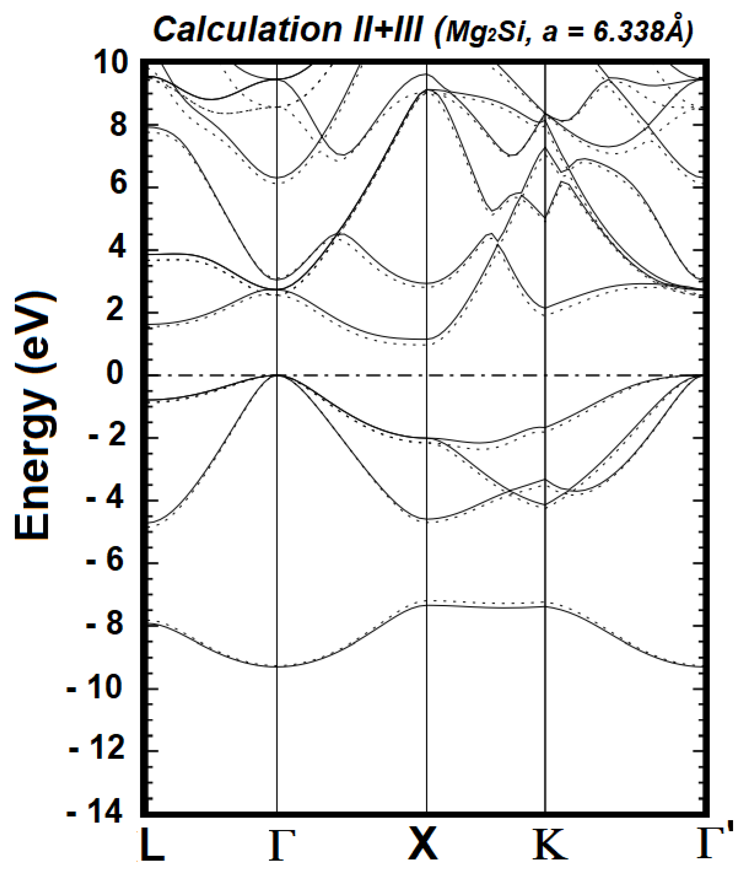
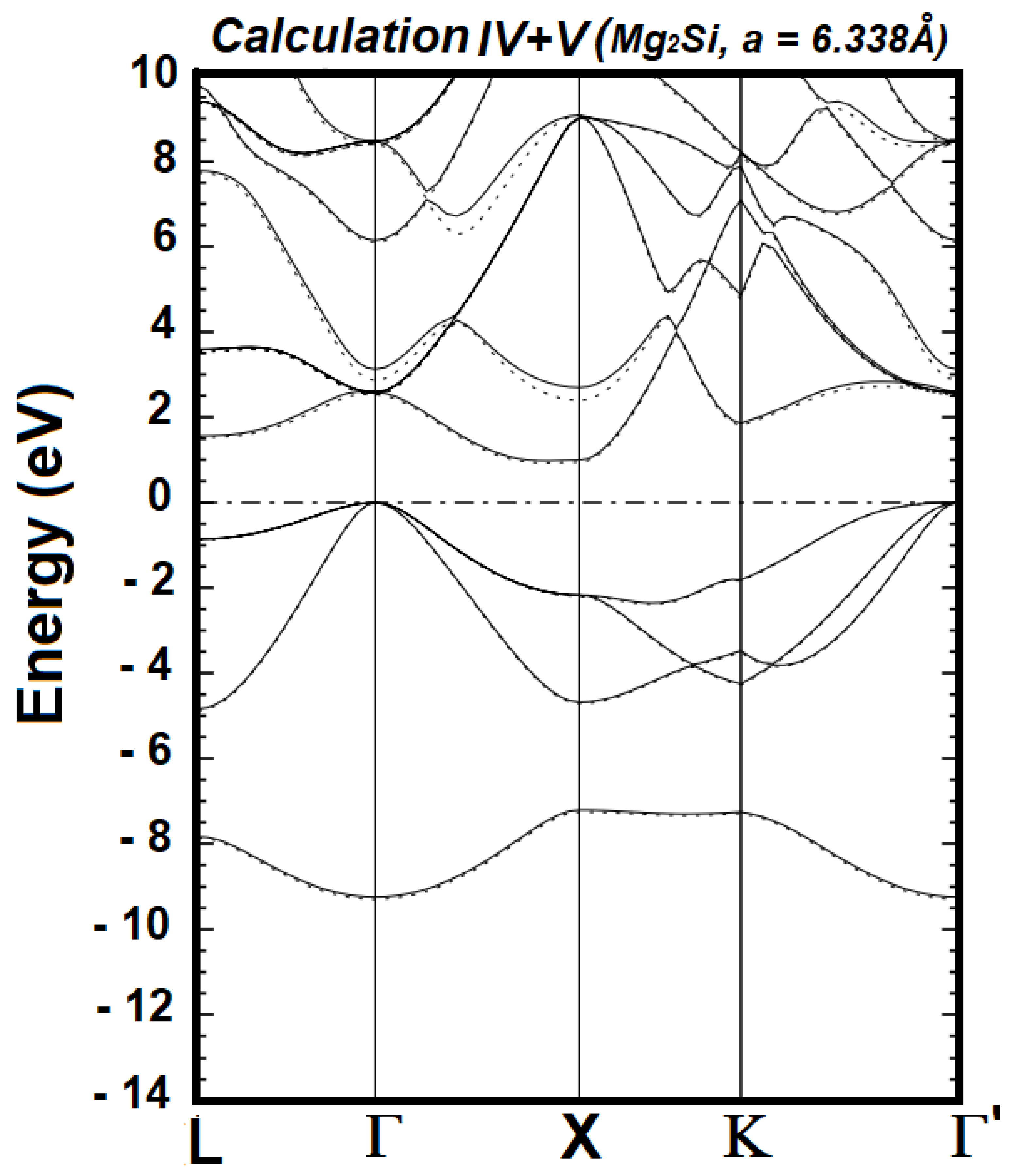
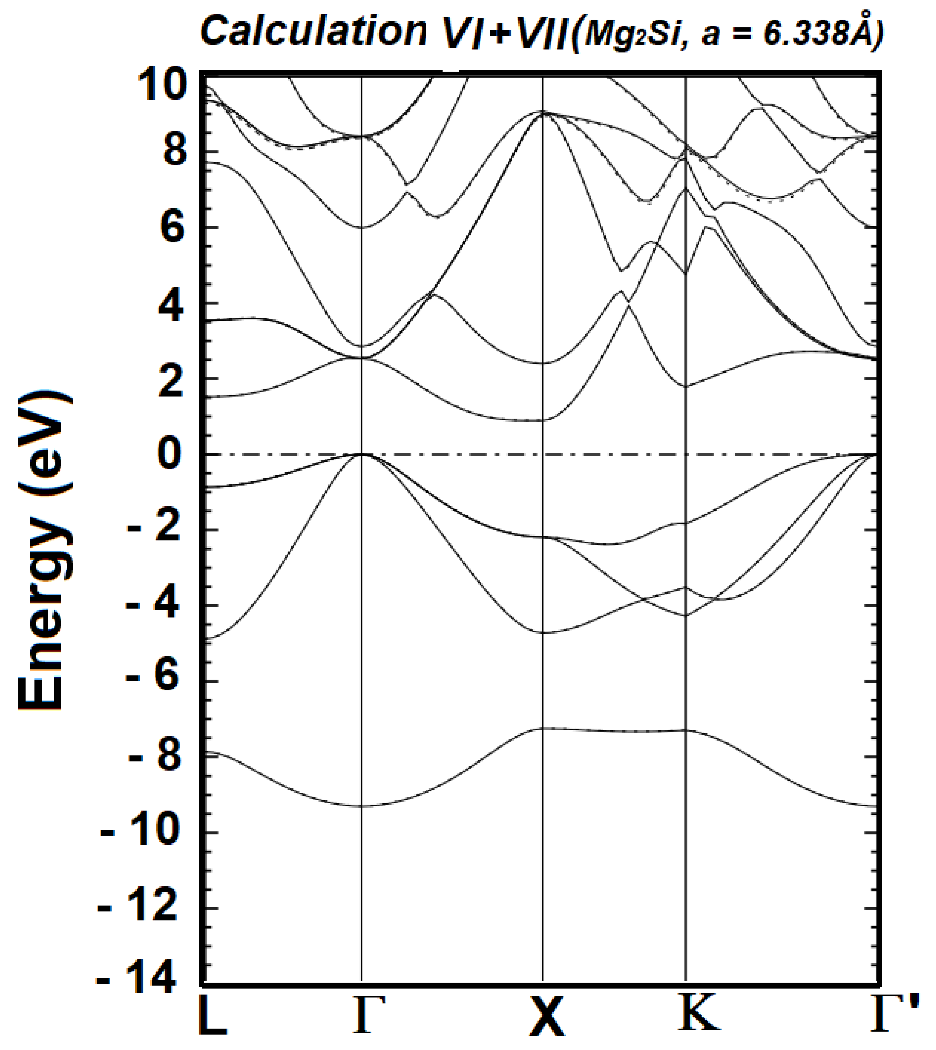
| Cal. No. | Orbitals for the Valence States of Mg1+ | Orbitals for the Valence States of Si2- | No. of Wave Functions | Band Gap (Γ–X) in eV | Band Gap (Γ–L) in eV |
|---|---|---|---|---|---|
| I | 2s2 2p6 3s1 | 2s2 2p6 3s2 3p4 | 36 | 0.3448 | 1.4000 |
| II | 2s2 2p6 3s1 3p0 | 2s2 2p6 3s2 3p4 | 48 | 1.1532 | 1.6275 |
| III | 2s2 2p6 3s1 3p0 | 2s2 2p6 3s2 3p4 4p0 | 54 | 0.9717 | 1.5560 |
| IV | 2s2 2p6 3s1 3p0 4p0 | 2s2 2p6 3s2 3p4 4p0 | 66 | 0.9949 | 1.5639 |
| V | 2s2 2p6 3s1 3p0 4p0 | 2s2 2p6 3s2 3p4 4p0 4s0 | 68 | 0.9434 | 1.5317 |
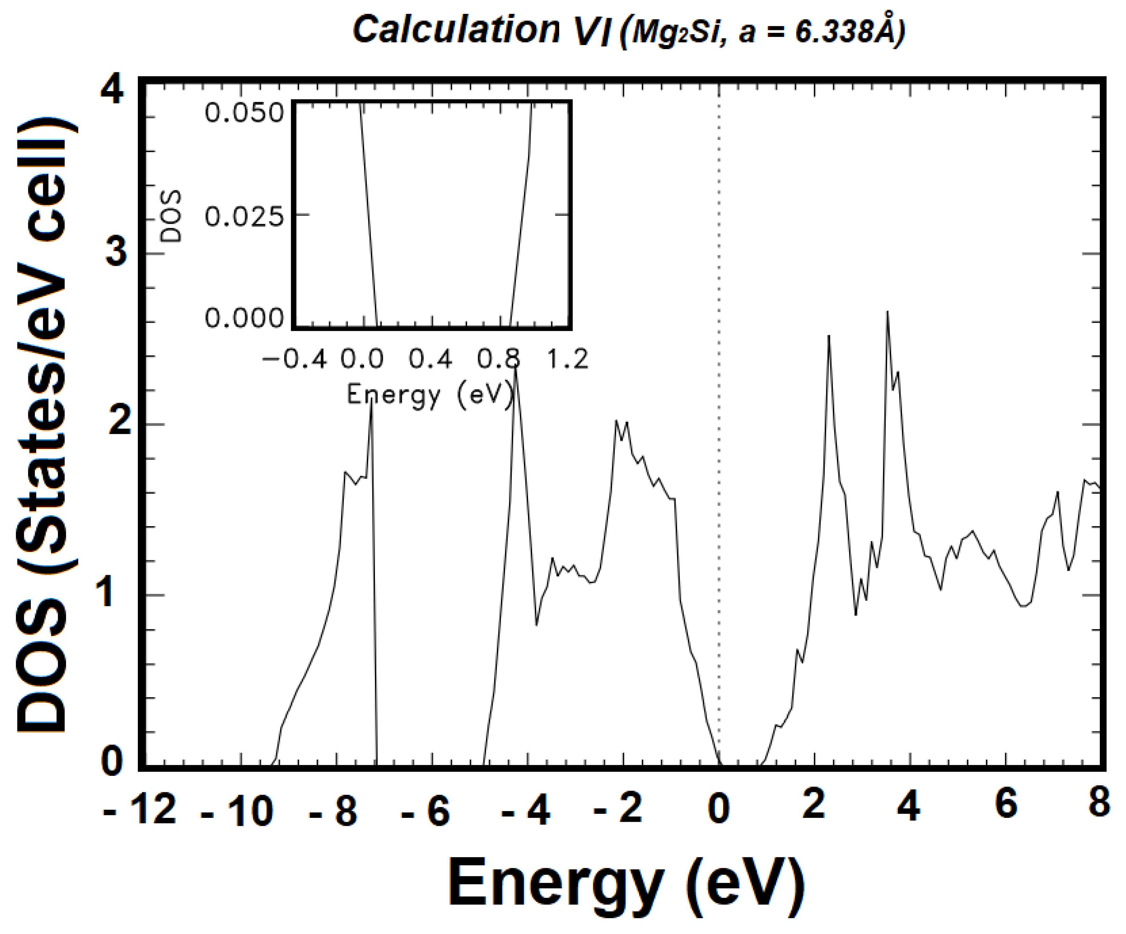
| VI | 2s22p63s13p04p04s0 | 2s22p63s23p44p04s0 | 72 | 0.8961 | 1.5219 |
| VII | 2s2 2p6 3s1 3p0 4p0 4s0 | 2s2 2p6 3s2 3p4 4p0 4s0 5p0 | 78 | 0.9040 | 1.5285 |
| VIII | 2s2 2p6 3s1 3p0 4p0 4s0 5p0 | 2s2 2p6 3s2 3p4 4p0 4s0 5p0 | 90 | 0.9048 | 1.5271 |
| L Point | Γ Point | X Point | K Point |
|---|---|---|---|
| 10.784 | 8.411 | 13.207 | 12.670 |
| 9.766 | 8.411 | 10.214 | 11.536 |
| 9.367 | 8.411 | 10.214 | 8.206 |
| 9.367 | 5.986 | 9.075 | 8.101 |
| 7.731 | 2.849 | 9.009 | 7.831 |
| 3.540 | 2.533 | 9.009 | 7.057 |
| 3.540 | 2.533 | 2.399 | 4.754 |
| 1.522 | 2.533 | 0.896 | 1.782 |
| −0.866 | 0.000 | −2.188 | −1.834 |
| −0.866 | 0.000 | −2.188 | −3.511 |
| −4.879 | 0.000 | −4.722 | −4.278 |
| −7.866 | −9.295 | −7.256 | −7.292 |
| Types and Directions of Effective Masses | Values of Effective Masses (mo) |
|---|---|
| me(Γ-L)111 | 0.418 |
| me(Γ-X)100 | 0.211 |
| me(Γ-K)110 | 0.247 |
| me(X-Γ) Longitudinal | 19.707 |
| me(X-W) Transverse | 0.171 |
| me(X-K) Transverse | 0.176 |
| me(L-Γ) Longitudinal | 3.420 |
| me(L-K) Transverse | 0.161 |
| me(L-W) Transverse | 0.173 |
| mhh1(Γ-L)111 | 0.838 |
| mhh1(Γ-X)100 | 0.288 |
| mhh1(Γ-K)110 | 0.516 |
| mhh2(Γ-K)110 | 0.327 |
| mlh(Γ-L)111 | 0.106 |
| mlh (Γ-X)100 | 0.183 |
| mlh (Γ-K)110 | 0.141 |
Disclaimer/Publisher’s Note: The statements, opinions and data contained in all publications are solely those of the individual author(s) and contributor(s) and not of MDPI and/or the editor(s). MDPI and/or the editor(s) disclaim responsibility for any injury to people or property resulting from any ideas, methods, instructions or products referred to in the content. |
© 2023 by the authors. Licensee MDPI, Basel, Switzerland. This article is an open access article distributed under the terms and conditions of the Creative Commons Attribution (CC BY) license (https://creativecommons.org/licenses/by/4.0/).
Share and Cite
Dioum, A.; Diakité, Y.I.; Malozovsky, Y.; Ayirizia, B.A.; Beye, A.C.; Bagayoko, D. First-Principles Investigation of Electronic and Related Properties of Cubic Magnesium Silicide (Mg2Si). Computation 2023, 11, 40. https://doi.org/10.3390/computation11020040
Dioum A, Diakité YI, Malozovsky Y, Ayirizia BA, Beye AC, Bagayoko D. First-Principles Investigation of Electronic and Related Properties of Cubic Magnesium Silicide (Mg2Si). Computation. 2023; 11(2):40. https://doi.org/10.3390/computation11020040
Chicago/Turabian StyleDioum, Allé, Yacouba I. Diakité, Yuiry Malozovsky, Blaise Awola Ayirizia, Aboubaker Chedikh Beye, and Diola Bagayoko. 2023. "First-Principles Investigation of Electronic and Related Properties of Cubic Magnesium Silicide (Mg2Si)" Computation 11, no. 2: 40. https://doi.org/10.3390/computation11020040