
Wideband E00-E10 Silicon Mode Converter Based on 180 nm CMOS Technology

 ,
,
Abstract
:1. Introduction
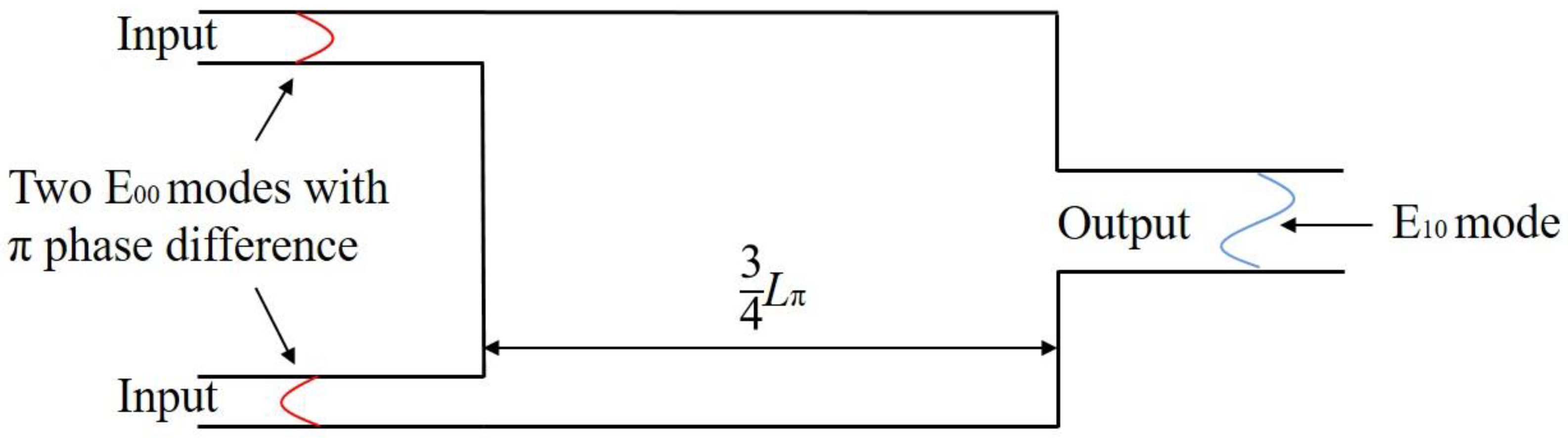
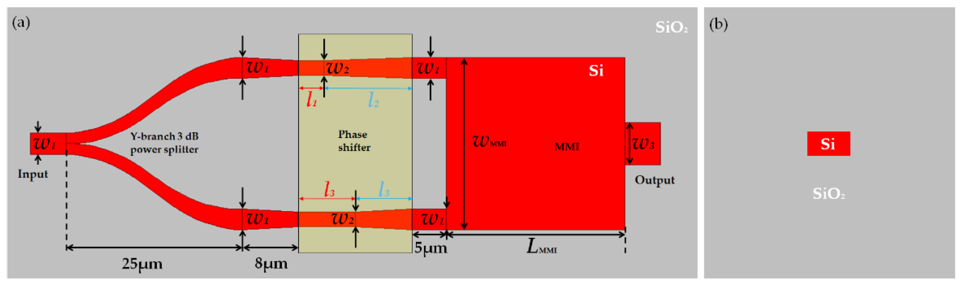
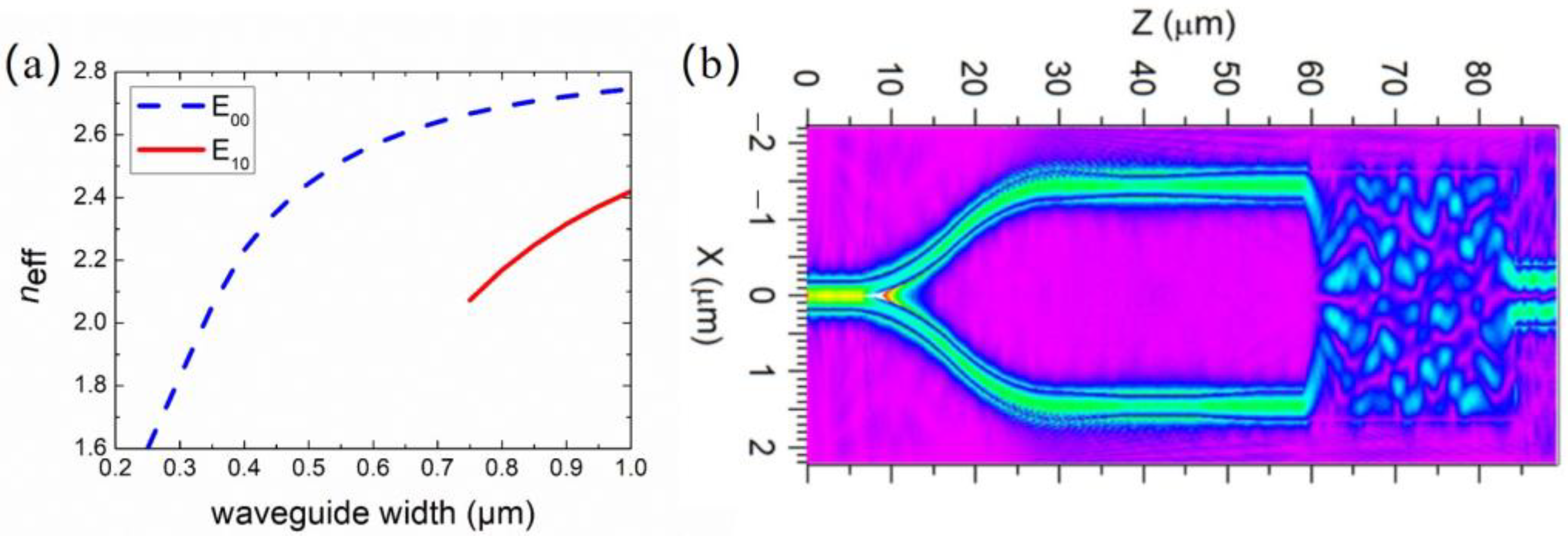
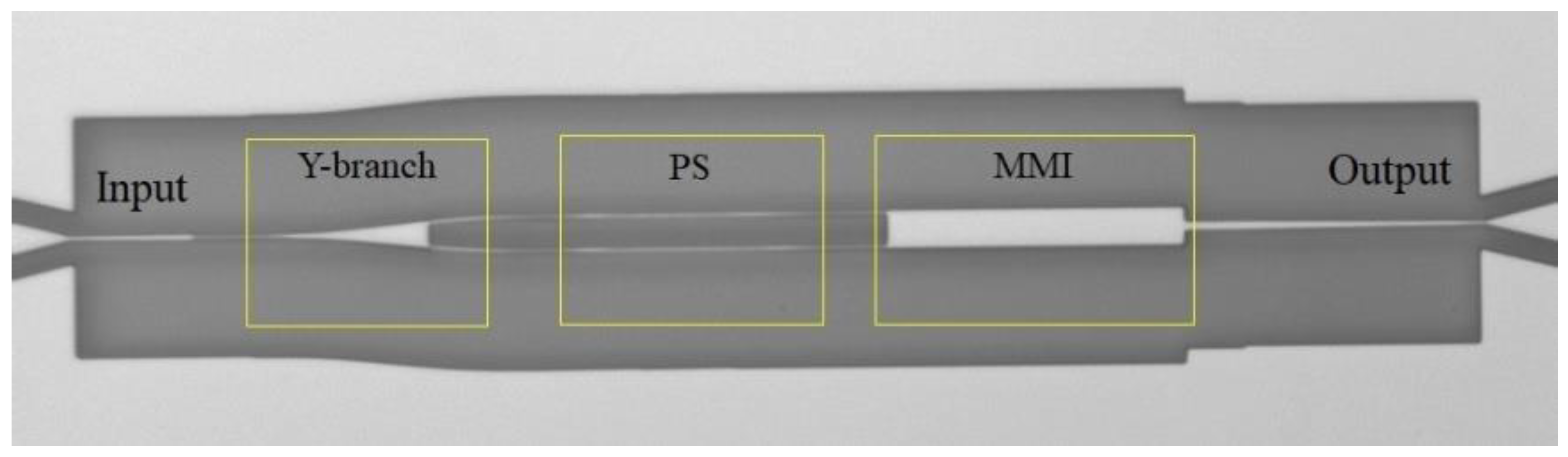
2. Device Design
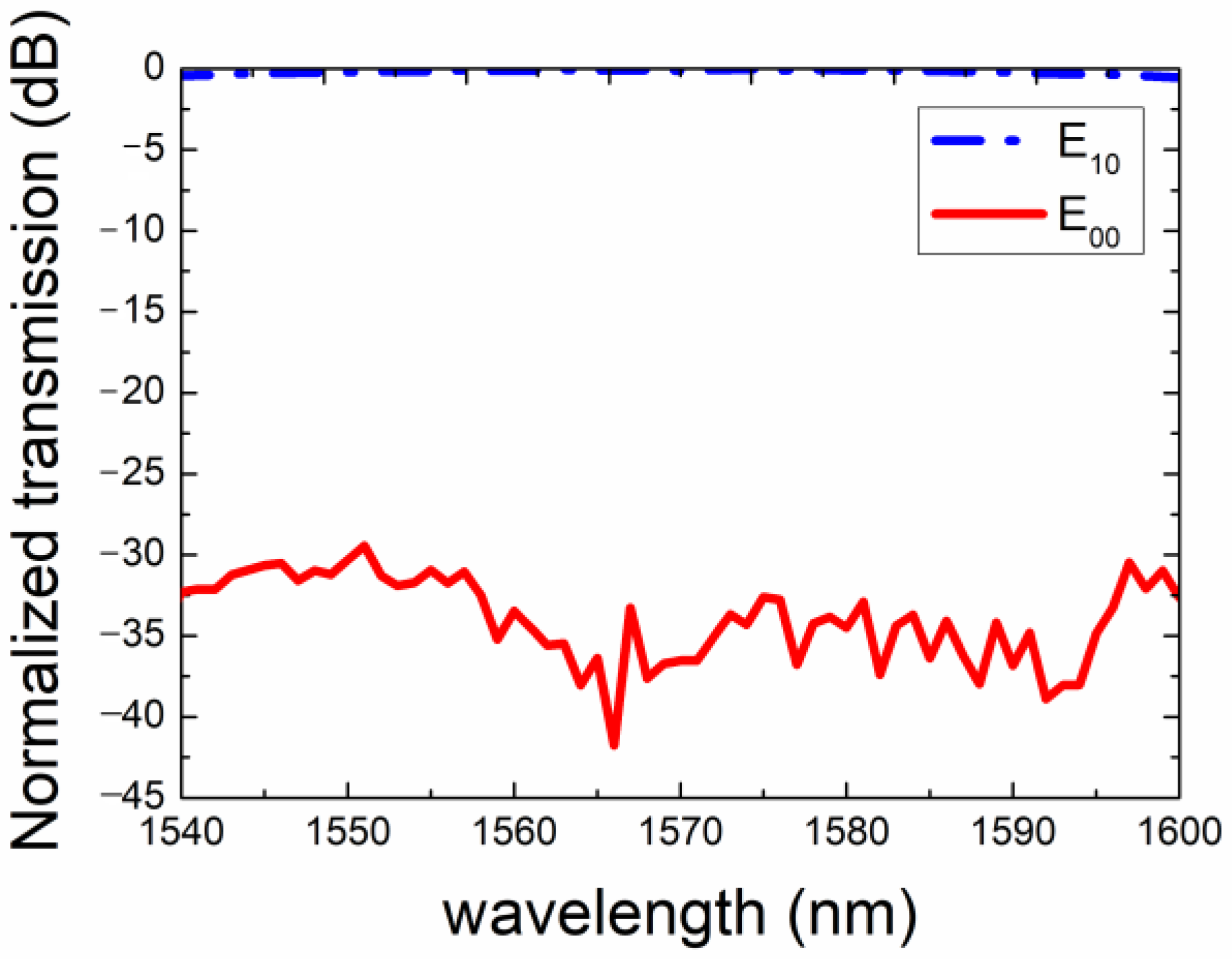
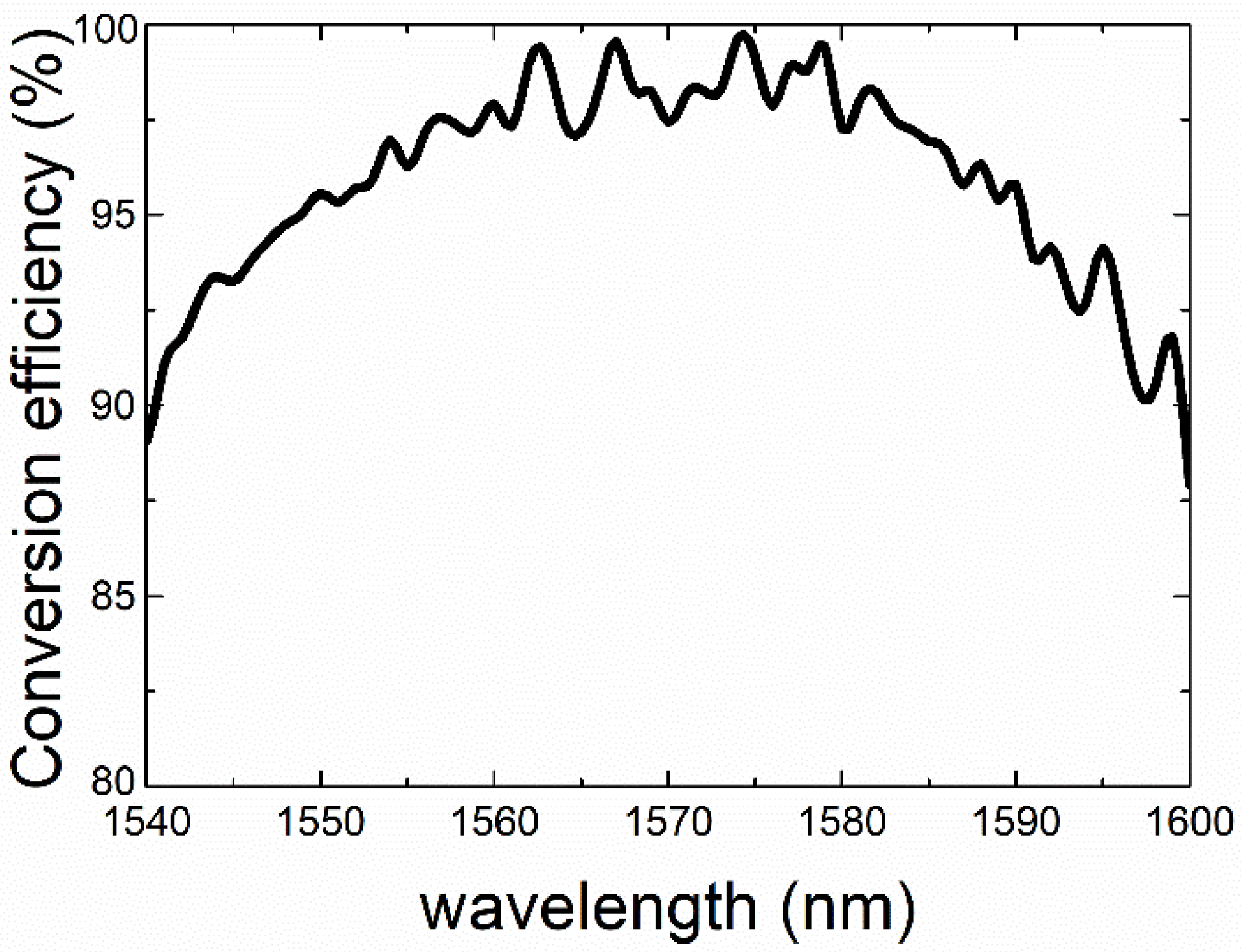
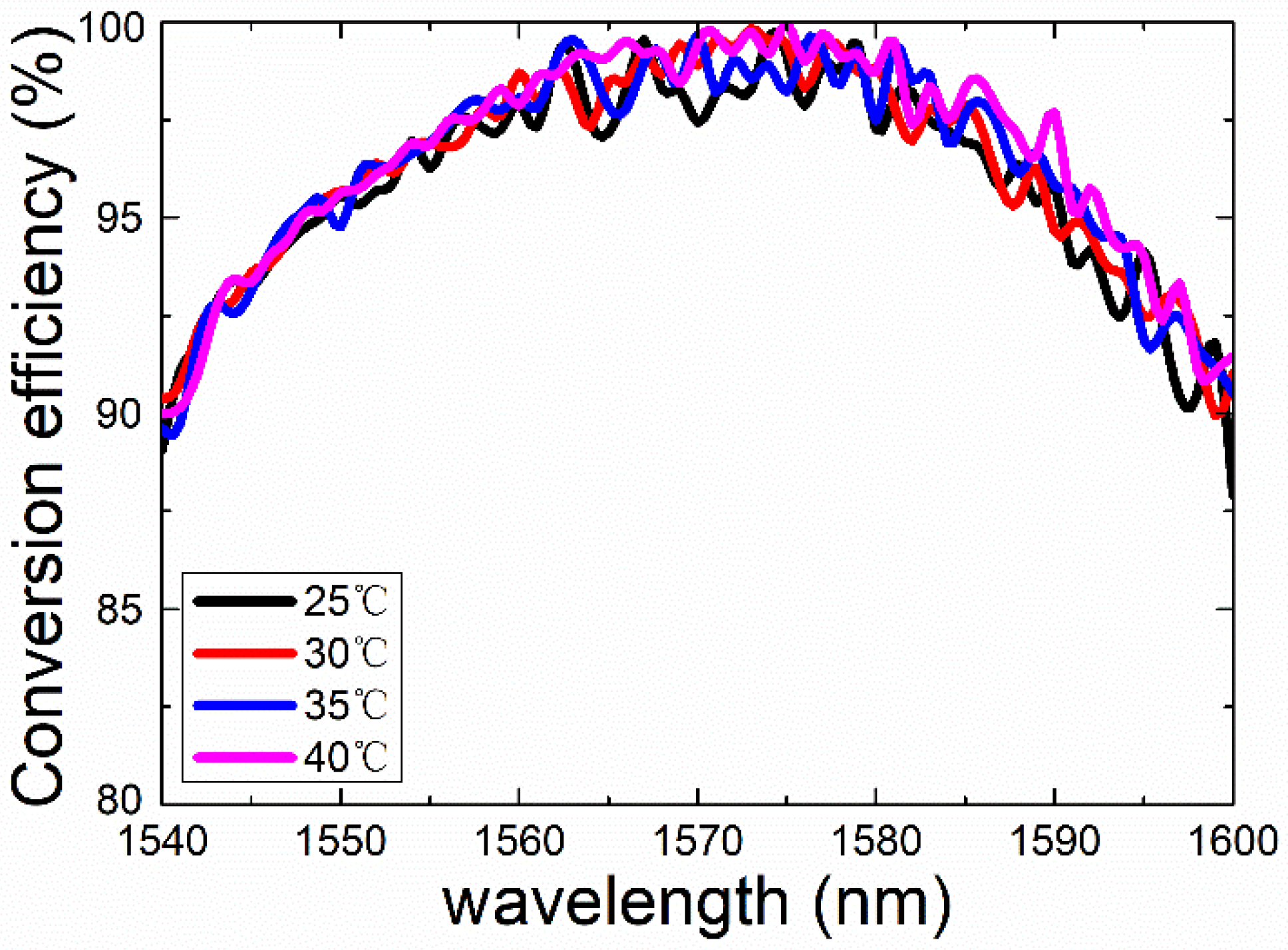
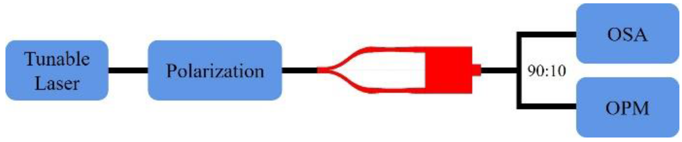
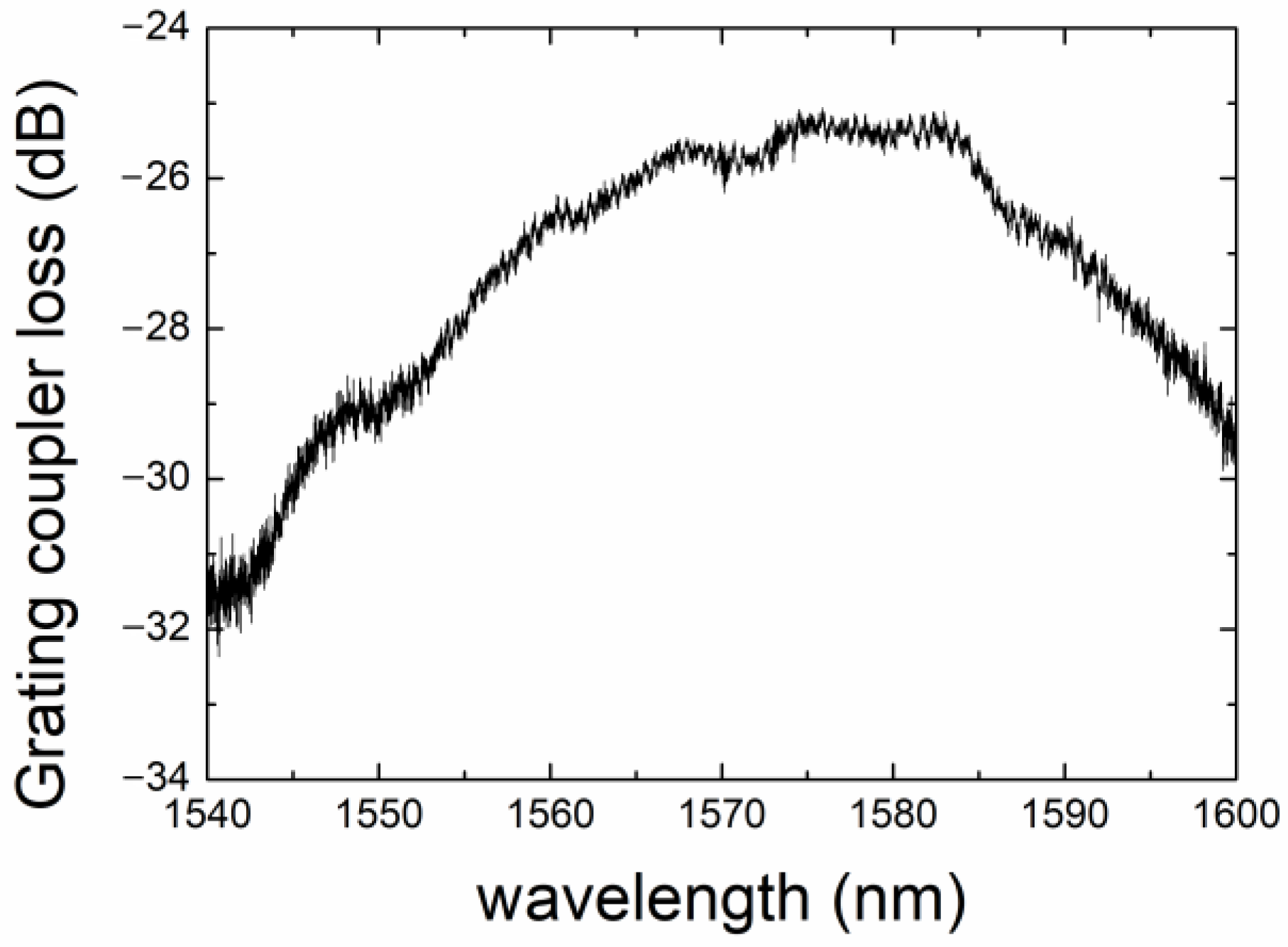
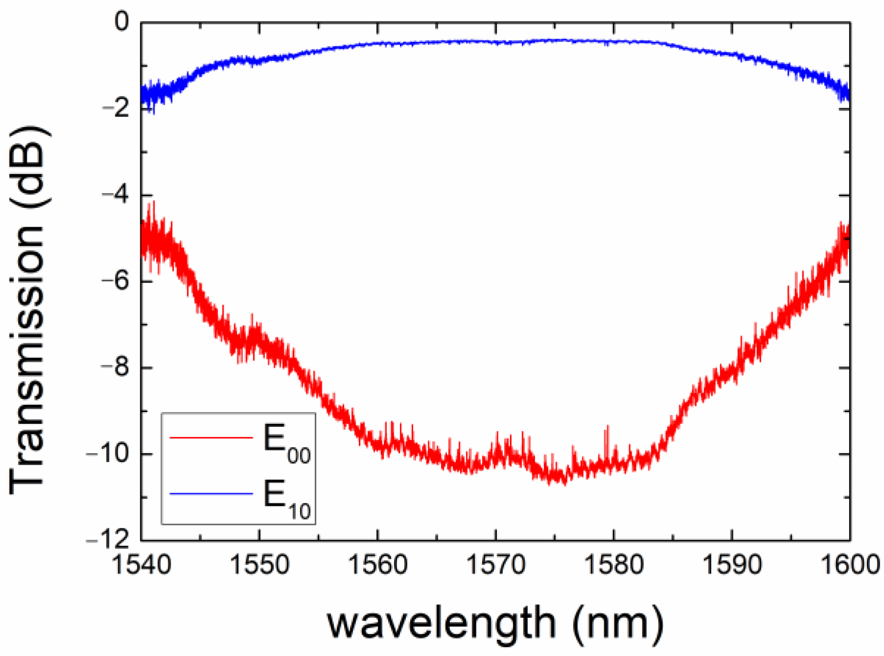
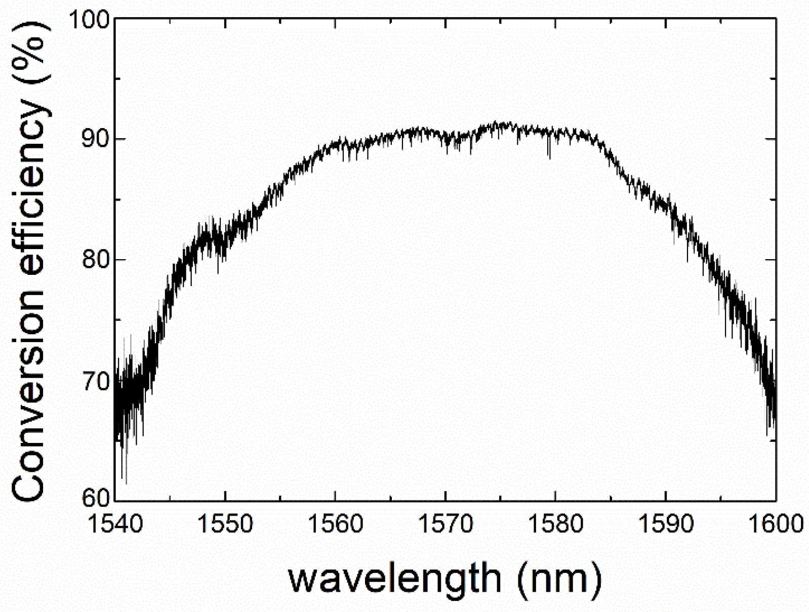
3. Results and Discussion
4. Conclusions
Author Contributions
Funding
Institutional Review Board Statement
Informed Consent Statement
Data Availability Statement
Conflicts of Interest
References
- Chun, H.; Rajbhandari, S.; Faulkner, G.; Tsonev, D.; Enyuan, X.; McKendry, J.J.D.; Gu, E.; Dawson, M.D.; O’Brien, D.C.; Haas, H. LED based wavelength division multiplexed 10 Gb/s visible light communications. J. Light. Technol. 2016, 34, 3047–3052. [Google Scholar] [CrossRef] [Green Version]
- Xing, F.; Chen, H.; Xie, S.; Yao, J. Ultrafast surface imaging with an increased spatial resolution based on polarization-division multiplexing. J. Light. Technol. 2015, 33, 396–402. [Google Scholar] [CrossRef]
- Zhang, Y.; Pan, S. Photonics-based multi-function analog signal processor based on a polarization division multiplexing Mach–Zehnder modulator. Opt. Lett. 2017, 42, 5034–5037. [Google Scholar] [CrossRef] [Green Version]
- Goossens, J.; Yousefi, M.; Jaouen, Y.; Hafermann, H. Polarization-division multiplexing based on the nonlinear Fourier transform. Opt. Express 2017, 25, 26437–26452. [Google Scholar] [CrossRef]
- Xiao, H.; Liu, Z.; Han, X.; Yang, J.; Ren, G.; Mitchell, A.; Tian, Y. On-chip reconfigurable and scalable optical mode multiplexer/demultiplexer based on three-waveguide-coupling structure. Opt. Express 2018, 26, 22366–22377. [Google Scholar] [CrossRef]
- Gao, Y.; Xu, Y.; Ji, L.; Sun, X.; Wang, F.; Wang, X.; Wu, Y.; Zhang, D. Scalable compact mode (de)multiplexer based on asymmetric Y-junctions. Opt. Commun. 2019, 438, 34–38. [Google Scholar] [CrossRef]
- Driscoll, J.B.; Chen, C.P.; Grote, R.R.; Souhan, B.; Dadap, J.I.; Stein, A.; Lu, M.; Bergman, K.; Osgood, R.M. A 60 Gb/s MDM-WDM Si photonic link with <0.7 dB power penalty per channel. Opt. Express 2014, 22, 18543–18555. [Google Scholar]
- Berdagué, S. Mode division multiplexing in optical fibers. Appl. Opt. 1982, 21, 1950. [Google Scholar] [CrossRef]
- Jiang, S.; Ma, L.; Zhang, Z.; Xu, X.; Wang, S.; Du, J.; Yang, C.; Tong, W.; He, Z. Design and characterization of ring-assisted few-mode fibers for weakly coupled mode-division multiplexing transmission. J. Light. Technol. 2018, 36, 5547–5555. [Google Scholar] [CrossRef]
- Ding, Y.; Xu, J.; Da Ros, F.; Huang, B.; Ou, H.; Peucheret, C. On-chip two-mode division multiplexing using tapered directional coupler-based mode multiplexer and demultiplexer. Opt. Express 2013, 21, 10376–10382. [Google Scholar] [CrossRef] [PubMed] [Green Version]
- Dai, D.; Li, C.; Wang, S.; Wu, H.; Shi, Y.; Wu, Z.; Gao, S.; Dai, T.; Yu, H.; Tsang, H. 10-channel mode (de)multiplexer with dual polarizations. Laser Photon. Rev. 2018, 12, 1700109. [Google Scholar] [CrossRef]
- Luo, L.W.; Ophir, N.; Chen, C.; Gabrielli, L.; Poitras, C.; Bergmen, K.; Lipson, M. WDM-compatible mode-division multiplexing on a silicon chip. Nat. Commun. 2014, 5, 3069. [Google Scholar] [CrossRef] [PubMed] [Green Version]
- Li, Y.; Li, C.; Li, C.; Cheng, B.; Xue, C. Compact two-mode (de)multiplexer based on symmetric Y-junction and multimode interference waveguides. Opt. Express 2014, 22, 5781–5786. [Google Scholar] [CrossRef] [PubMed]
- Gao, Y.; Sun, X.; Li, P.; Zhang, D. Polymer mode selecting switch based on cascaded MMI couplers. IEEE Photon. Technol. Lett. 2021, 33, 147–150. [Google Scholar] [CrossRef]
- Sun, Y.; Xiong, Y.; Ye, W.N. Experimental demonstration of a two-mode (de)multiplexer based on a taper-etched directional coupler. Opt. Lett. 2016, 41, 3743–3746. [Google Scholar] [CrossRef] [PubMed]
- Chen, W.; Wang, P.; Yang, T.; Wang, G.; Dai, T.; Zhang, Y.; Zhou, L.; Jiang, X.; Yang, J. Silicon three-mode (de)multiplexer based on cascaded asymmetric Y junctions. Opt. Lett. 2016, 41, 2851–2854. [Google Scholar] [CrossRef]
- Zhang, Z.; Yu, Y.; Fu, S. Broadband on-chip mode-division multiplexer based on adiabatic couplers and symmetric Y-junction. IEEE Photonics J. 2017, 9, 6600406. [Google Scholar]
- Jia, H.; Fu, X.; Zhou, T.; Zhang, L.; Yang, S.; Yang, L. Mode-selective modulation by silicon microring resonators and mode multiplexers for on-chip optical interconnect. Opt. Express 2019, 27, 2915–2925. [Google Scholar] [CrossRef]
- Xiao, H.; Zhang, Z.; Yang, J.; Han, X.; Chen, W.; Ren, G.; Mitchell, A.; Yang, J.; Gao, D.; Tian, Y. On-chip scalable mode-selective converter based on asymmetrical micro-racetrack resonators. Nanophotonics 2020, 9, 1447. [Google Scholar] [CrossRef]
- Ye, M.; Yu, Y.; Chen, G.; Luo, Y.; Zhang, X. On-chip WDM mode-division multiplexing interconnection with optional demodulation function. Opt. Express 2015, 23, 32130–32138. [Google Scholar] [CrossRef]
- Qiu, H.; Yu, H.; Hu, T.; Jiang, G.; Shao, H.; Yu, P.; Yang, J.; Jiang, X. Silicon mode multi/demultiplexer based on multimode grating-assisted couplers. Opt. Express 2013, 21, 17904–17911. [Google Scholar] [CrossRef] [PubMed]
- Gui, C.; Gao, Y.; Zhang, Z.; Wang, J. On-chip silicon two-mode (de)multiplexer for OFDM/OQAM data transmission based on grating-assisted coupler. IEEE Photon. J. 2015, 7, 7905807. [Google Scholar] [CrossRef]
- He, Y.; Zhang, Y.; Wang, H.; Sun, L.; Su, Y. Design and experimental demonstration of a silicon multi-dimensional (de)multiplexer for wavelength-, mode- and polarization-division (de)multiplexing. Opt. Lett. 2020, 45, 2846–2849. [Google Scholar] [CrossRef] [PubMed]
- Xie, H.; Liu, Y.; Wang, S.; Wang, Y.; Yao, Y.; Song, Q.; Du, J.; He, Z.; Xu, K. Highly compact and efficient four-mode multiplexer based on pixelated waveguides. IEEE Photon. Technol. Lett. 2020, 32, 166–169. [Google Scholar] [CrossRef]
- Wang, J.; Zhai, Y.; Mao, J.; Lu, Y.; Xu, J.; Dai, D. Silicon-nanowire-based optical hybrid with insensitive operation for TE/TM states of polarization. Opt. Commun. 2017, 385, 124–129. [Google Scholar] [CrossRef]
- Wang, H.; Zhang, Y.; He, Y.; Zhu, Q.; Sun, L.; Su, Y. Compact silicon waveguide mode converter employing dielectric metasurface structure. Adv. Opt. Mater. 2019, 7, 1801191. [Google Scholar] [CrossRef]
- Gao, Y.; Zhang, D.; Xu, Y.; Fan, X.; Wang, F.; Sun, X. Ultra-broadband polymer E00/E10 mode converter. Opt. Commun. 2022, 508, 127715. [Google Scholar] [CrossRef]
- Guzman-Chavez, A.D.; Vargas-Rodriguez, E. Enhanced thermally tunable optical filter and its applications in Erbium-doped fiber lasers. IEEE Photon. Technol. Lett. 2020, 32, 297–300. [Google Scholar] [CrossRef]
- Wang, T.; Guo, H.; Chen, H.; Yang, J.; Jia, H. Ultra-compact reflective mode converter based on a silicon subwavelength structure. Appl. Opt. 2020, 59, 2754–2758. [Google Scholar] [CrossRef]
- Zhao, Y.; Guo, X.; Zhang, Y.; Xiang, J.; Wang, K.; Wang, H.; Su, Y. Ultra-compact silicon mode-order converters based on dielectric slots. Opt. Lett. 2020, 45, 3797–3800. [Google Scholar] [CrossRef]
- Frandsen, L.H.; Elesin, Y.; Frellsen, L.F.; Mitrovic, M.; Ding, Y.H.; Sigmund, O.; Yvind, K. Topology optimized mode conversion in a photonic crystal waveguide fabricated in silicon-on-insulator material. Opt. Express 2014, 22, 8525–8532. [Google Scholar] [CrossRef] [PubMed]


| Ref. | Footprint (μm2) | Insert Loss (dB) | Crosstalk (dB) | BW (nm) | Structure | Materials |
|---|---|---|---|---|---|---|
| [29] | 2 × 2 | 2.2 | −16.2 | 40 | Inversely design | SOI |
| [30] | 0.8 × 1.2 | <1.2 | / | 50 | Slots waveguide | SOI |
| [31] | 6.3 × 3.6 | 2 | −12 | 43 | Photonic crystal waveguide | SOI |
| This work | 3.3 × 79.3 | 0.4–2 | >−10.3 | >60 | PS + MMI | SOI |
Publisher’s Note: MDPI stays neutral with regard to jurisdictional claims in published maps and institutional affiliations. |
© 2022 by the authors. Licensee MDPI, Basel, Switzerland. This article is an open access article distributed under the terms and conditions of the Creative Commons Attribution (CC BY) license (https://creativecommons.org/licenses/by/4.0/).
Share and Cite
Xu, Y.; Gao, Y.; Liu, S.; Liu, T.; Sun, X.; Tang, B.; Zhang, P.; Zhang, D. Wideband E00-E10 Silicon Mode Converter Based on 180 nm CMOS Technology. Appl. Sci. 2022, 12, 10688. https://doi.org/10.3390/app122010688
Xu Y, Gao Y, Liu S, Liu T, Sun X, Tang B, Zhang P, Zhang D. Wideband E00-E10 Silicon Mode Converter Based on 180 nm CMOS Technology. Applied Sciences. 2022; 12(20):10688. https://doi.org/10.3390/app122010688
Chicago/Turabian StyleXu, Yan, Yang Gao, Songyue Liu, Tingyu Liu, Xiaoqiang Sun, Bo Tang, Peng Zhang, and Daming Zhang. 2022. "Wideband E00-E10 Silicon Mode Converter Based on 180 nm CMOS Technology" Applied Sciences 12, no. 20: 10688. https://doi.org/10.3390/app122010688