Article

Ultra-Compact Digital Metasurface Polarization Beam Splitter via Physics-Constrained Inverse Design

1
Shanghai Institute of Applied Physics, Chinese Academy of Sciences, Shanghai 201800, China
2
University of Chinese Academy of Sciences, Beijing 100049, China
3
Zhejiang Lab, Hangzhou 311100, China
4
Shanghai Synchrotron Radiation Facility, Shanghai Advanced Research Institute, Chinese Academy of Sciences, Shanghai 201204, China
*
Authors to whom correspondence should be addressed.
Appl. Sci. 2022, 12(19), 10064; https://doi.org/10.3390/app121910064
Submission received: 16 September 2022 / Revised: 2 October 2022 / Accepted: 3 October 2022 / Published: 7 October 2022
(This article belongs to the Special Issue Laser and Silicon Photonics: Technology, Preparation and Application)

Abstract

:
Inverse design effectively promotes the miniaturization of integrated photonic devices through the modulation of subwavelength structures. Utilizing a theoretical prior based inverse design, we propose an ultra-compact integrated polarizing beam splitter consisting of a standard silicon-on-insulator (SOI) substrate and a tunable air–silicon column two-dimensional code metasurface, with a footprint of 5 × 2.7 μm2. The effective refractive index of the waveguide is modulated by adjusting the two-dimensional code morphology in the additional layer to achieve efficient polarization beam splitting. The simulation results demonstrate high performance, with a low insertion loss (<0.87 dB) and high extinction ratio (>10.76 dB) in a bandwidth of 80 nm covering the C-band. The device can withstand manufacturing errors up to ±20 nm and is robust to process defects, such as the outer proximity effect, and thus is suitable for ultra-compact on-chip optical interconnects.

1. Introduction

Silicon photonics has many promising potentials because of its compact footprint and CMOS compatibility [1,2,3,4,5]. Silicon-on-insulator (SOI), as the main material system applicable in integrated photonics, stands out for utilizing the advantages of its high speed and large bandwidth of light, which will further improve the information processing and transmission speed of integrated circuits and reduce power consumption [6,7,8,9]. However, most silicon photonics devices are generally very sensitive to polarization. A potentially effective approach is to split the light of different polarization modes into devices that process different polarization states separately, thereby requiring efficient and compact polarization beam splitters (PBS) [10,11]. The working principle of traditional on-chip compact PBSs is usually based on modal evolution [12] or interferometry, including asymmetric directional couplers (ADCs) [13,14,15,16,17,18,19,20,21], Mach-Zehnder interferometers (MZIs) [22,23,24], photonic crystal waveguides [17], multi-mode interference couplers (MMIs) [25,26], etc. However, the strict phase-matching principle leads to stringent fabrication precision, and the relatively large footprint of these devices limits their potential for further compact integration on-chip. In recent years, the introduction of subwavelength structures has brought new degrees of freedom into the design of photonic devices, effectively promoting the miniaturization of silicon photonics devices and their further dense integration on-chip, which provides an attractive way for the design and optimization of ultra-compact and high-performance PBS devices [6,27,28,29].
The current design of subwavelength devices is usually based on inverse design, thereby allowing the geometry of the metamaterials to be freely optimized, which opens up a larger parameter space and can obtain a very fine structure through optimization [10,30,31,32,33,34,35]. Making full use of the existing high-precision manufacturing process and high-performance computing capabilities, the designed devices have been proven to have the advantages of small footprints, high performance, and multiple degrees of freedom in the design process [36,37]. Utilizing a non-linear search algorithm based on a direct-binary search, Shen and co-workers proposed an ultra-compact PBS with a footprint of 2.4 × 2.4 μm2 and an extinction ratio greater than 10 dB within a bandwidth of 32 nm [10]. Wei and colleagues proposed a 3D-printed PBS in the near-infrared with extinction ratios as much as 5 dB at the optimal wavelength [32]. However, we note that the existing research utilizing inverse design mostly considered the sophisticated optical response of nanostructured arrays as a mathematical optimization aiming at device output power under a two-dimensional approximation. Various algorithms (binary search algorithm (DBS), genetic algorithm, gradient descent, etc.) were applied to optimize a predefined figure of merit (FOM) and give a definite result, which cannot match the corresponding physical interpretation. Therefore, these methods have relatively low design diversity and high demand for computing power. The computational complexity increases exponentially with the increase in nanostructure size and the introduction of multi-parameter or multi-dimensional optimization objectives. Since the completely non-physical structure optimization process lacks upper-level guidance, some blind and inefficient operations need to be performed in the initial stage, leading to a waste of computing power. To solve these problems, a physical-model-guided inverse design method is needed, which can provide more constraints for the optimization process while retaining the advantages of the high degree of freedom in the design process and large optimization space of inversely designed components.
In this work, we propose a digital two-dimensional code metasurface PBS based on a gradient index, which was inspired by the theoretical experience of our previous work [38]. The physical model of the gradient refractive index is determined by theoretical analysis, which effectively avoids the solutions being trapped in local optimums and gets rid of the uncertainty resulting from the sensitivity to stochastic initial values. Through further optimization, the topographic structure of the two-dimensional code array of the metasurface layer is adjusted to realize the local effective mode refractive index modulation of the waveguide layer within this limited range. This design method reflects a high degree of design freedom, a large optimization potential, and a small dependence on computing power. We demonstrate a novel PBS structure with a minimum 2.7 × 5 μm2 footprint. The metasurface structure obtained by the inverse design is directly built on the 220 nm thick SOI waveguide, which acts as a 120 nm thick additional material layer. Therefore, the effective refractive index distribution of the waveguide is regulated by a two-dimensional code metasurface layer consisting of thousands of pixels. The simulation result shows a low insertion loss (IL) that is less than 0.73 dB and 0.87 dB, and a high extinction ratio (ER) that is greater than 12.59 dB and 10.76 dB for the TE and TM modes, respectively. Note that the device has a high performance under broadband inputs (1510 nm to 1590 nm, covering the C-band). In addition, we also demonstrate the device performance under certain manufacturing errors, and the simulation results indicate that the device has good performance and large manufacturing tolerances.

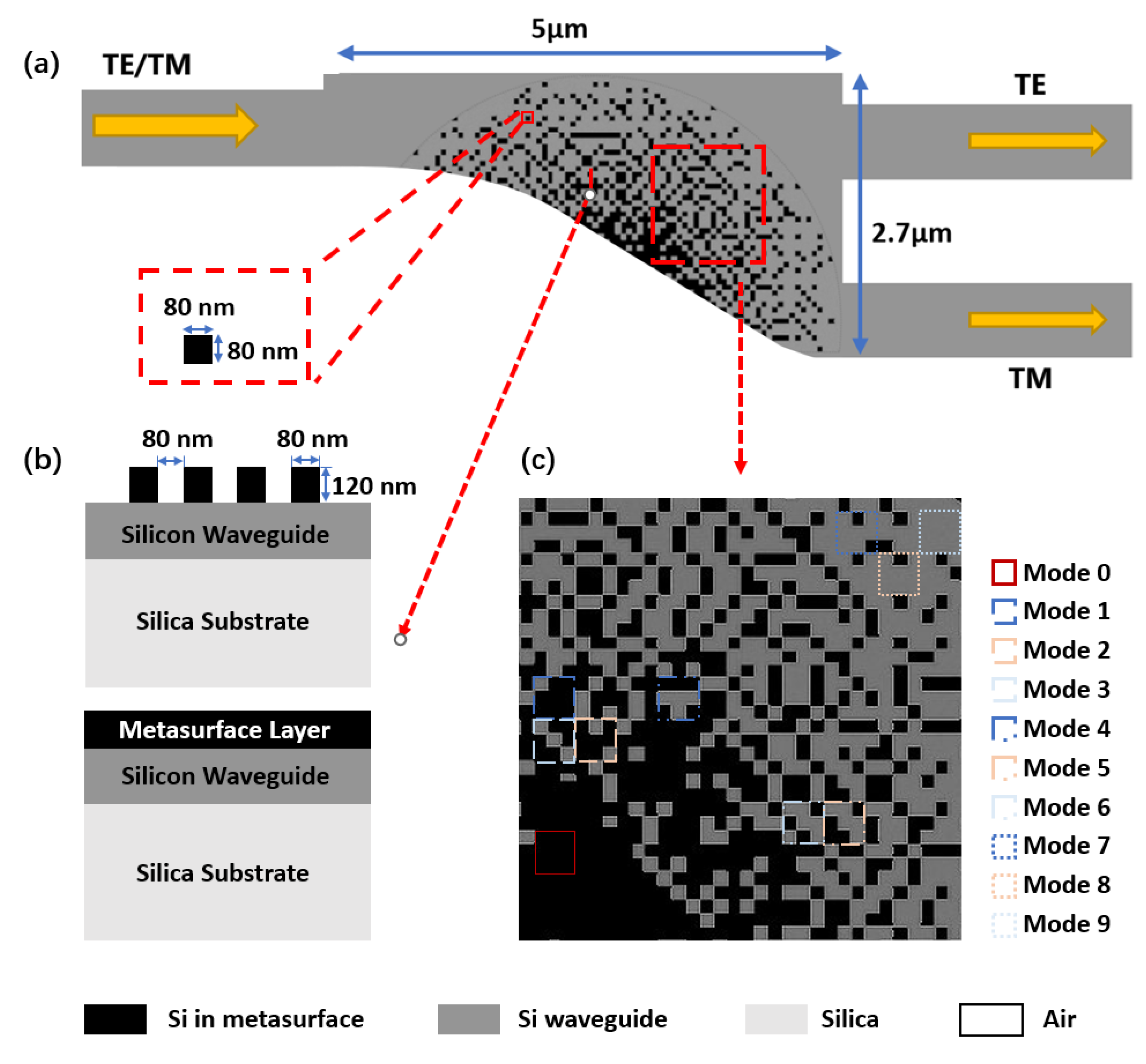
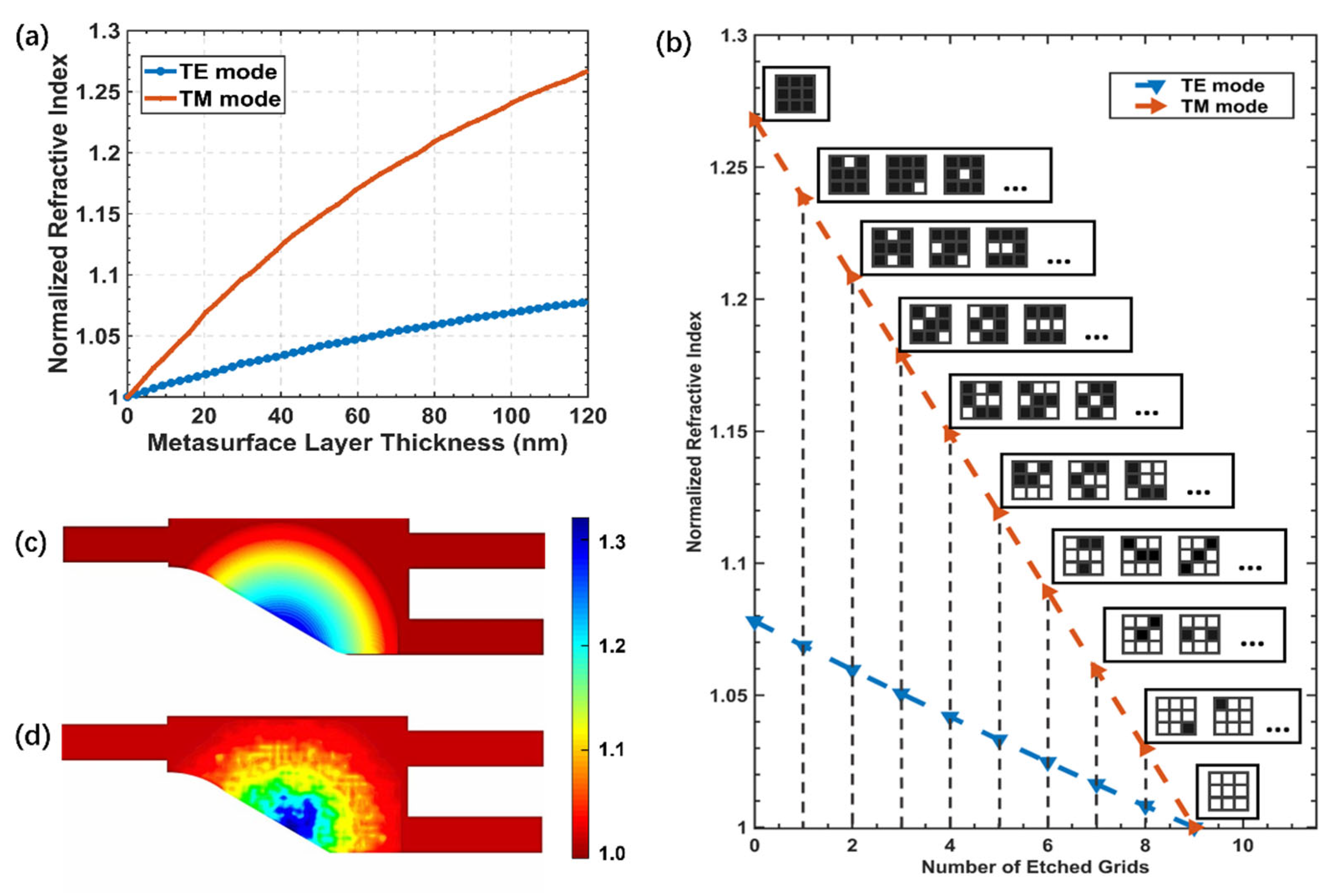
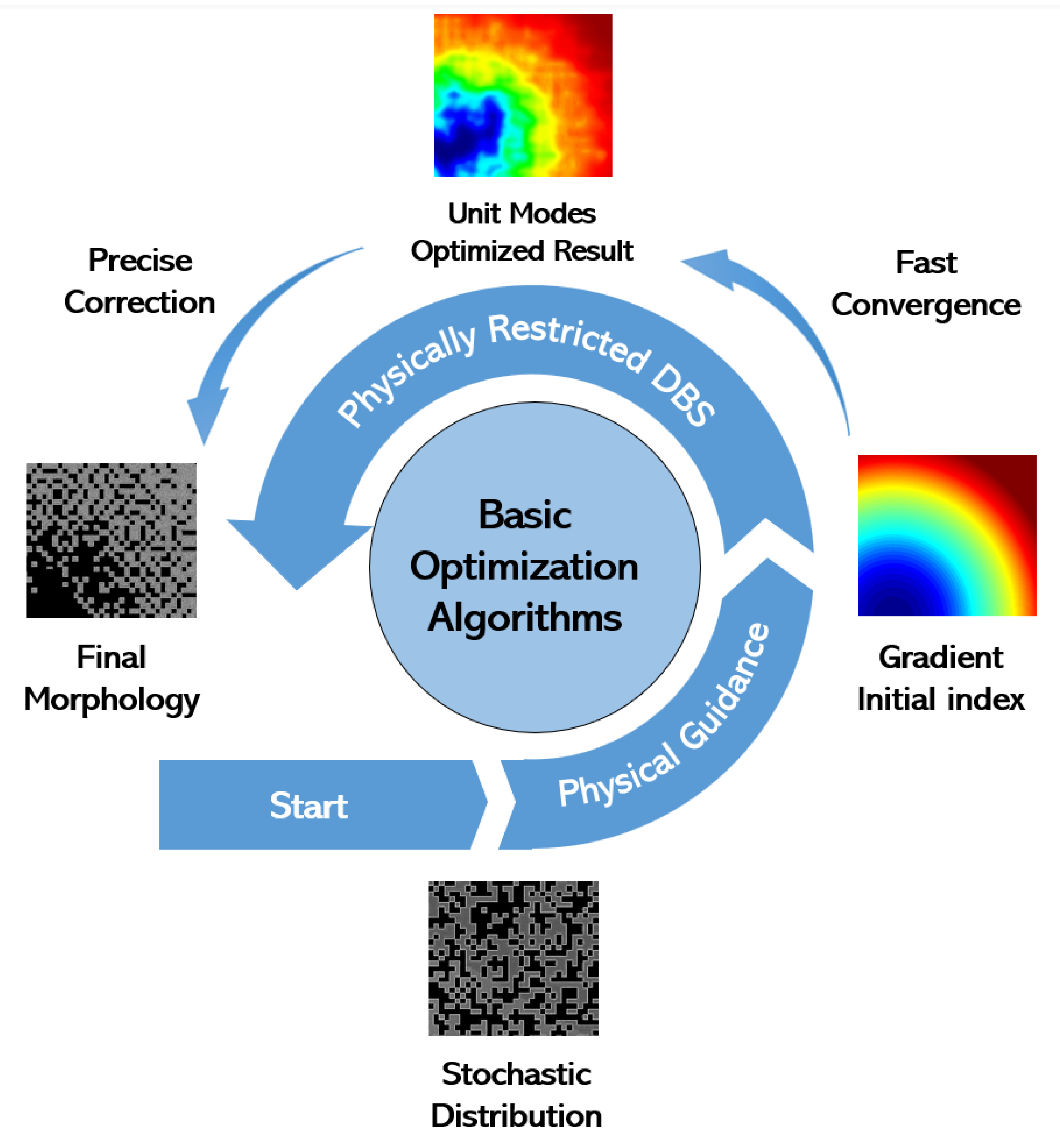
2. Structure and Method

Figure 1a,b shows the proposed PBS, which is realized by utilizing a 120 nm metasurface structure formed on a standard commercial SOI platform. Incident light with both TE and TM polarization enters the metasurface PBS from the input port, which is a silicon waveguide of 220 nm thickness, while the effective refractive index of the waveguide is modulated by adjusting the distribution of the subwavelength structure. Then, TE and TM modes are separated due to the different responses to the metasurface and then separate into different output ports. The footprint of the device is as compact as 2.7 × 5 μm2. The metasurface layer, as shown in Figure 1c, is a two-dimensional code structure composed of a cylindrical silicon layer with a diameter of 5 μm and a number of unevenly distributed square air holes etched inside. The square air holes have a side length of 80 nm, which is far below the working wavelength. According to the law of medium equivalence, a certain uniformly-changed, isotropic refractive index profile can be achieved by changing the topographic structure of the metasurface layer [39].
Owing to the strong birefringence of silicon, TE and TM polarized light reflect different effective indices when transmitted in the same waveguide. The propagation of light from different polarizations in the waveguide follows for the TE and TM modes, respectively:
n silicon 2 N TM 2 1 / 2 k 0 h = m π + tan 1 n silicon 2 n silica 2 N TM 2 n silica 2 n silicon 2 N TM 2 + tan 1 n silicon 2 n air 2 N TM 2 n air 2 n silicon 2 N TM 2 n silicon 2 N TE 2 1 / 2 k 0 h = m π + tan 1 N TE 2 n silica 2 n silicon 2 N TE 2 + tan 1 N TE 2 n air 2 n silicon 2 N TE 2
Here, NTE and NTM is the effective refractive index of the two polarization modes, k0 represents the wavenumber when light propagates in a vacuum, and h indicates the thickness of the waveguide.
Therefore, the effective refractive indices of different modes of light have different responses to the equivalent thickness h of the waveguide layer, which is determined by the thickness of the additional metasurface layer in the considered PBS. Figure 2a shows the variation curve of the effective refractive index with the thickness of the silicon-based metasurface layer, where a relationship of positive correlation can be observed. As the thickness increases, the difference between the effective refractive indices in different polarization modes gradually increases, which is beneficial for the output of the TE and TM modes to different ports. With a reasonable manufacturing difficulty, the variation ranges of the effective indices are considered for the selection of as many possibilities for the optical path modulation by the additional layer with a structure of two-dimensional code. Therefore, the thickness of the additional silicon layer is set to 120 nm, where the maximum relative effective refractive index of the TE mode is 1.08 and that of the TM mode is 1.27.
The digital two-dimensional code metasurface structure is used to set the refractive index with a high degree of freedom and large parameter space. The length of the minimum etched cell in the two-dimensional code is set to 80 nm, which is far below the operating wavelength. Therefore, the considered device is discretized into thousands of 80 nm × 80 nm silicon/air pillars, which are defined as “pixels”. Each such pixel can occupy two states: silicon or air. Here, by setting the limit of the gradient refractive index, we realize the optimization of the metasurface structure without high computing power while retaining high manufacturing tolerance. The dielectric constants of the different polarized lights in the doped medium are [40]:
ε TE = p ε air + 1 p ε silicon 1 ε TM = p ε air + 1 p ε silicon
where p is the volume fraction, which is defined as the area ratio of the air holes in the specified unit area in the two-dimensional case. For optical materials, the effective refractive index N is numerically equal to the square root of the dielectric constant ε. The regulation of the air volume fraction of the surface area of the metamaterial is realized by nanostructure arrays that can be regarded as a two-dimensional code distribution. The metasurface silicon layer with a thickness of 120 nm is divided into a series of square units with a side length of 240 nm, and each unit is further divided into a nine-square lattice structure of 3 × 3 small pixels. Then, the local approximate thickness can be adjusted by determining the number of etched pixels in each unit, thereby realizing the different local efficient refractive indices in the corresponding area. The number of etched pixels in each unit ranges from 0 to 9. It can be seen from the figure that as the number of etched cells in each unit decreases, the corresponding local effective refractive index increases, and the index difference between the TE and TM modes in the unit gradually increases. As a result, light of different polarizations can be deflected by different degrees in the waveguide layer. Therefore, the local effective refractive indices of each cell can be divided into 10 density modes, and the corresponding effective refractive index is shown in Figure 2b. Except for mode 0 (none of the pixels are etched) and mode 9 (all the pixels are etched), each mode has several possible code arrangements with an equivalent local refractive index.
As can be observed in natural phenomena such as mirages, light travels along a curved path in a variable index medium, and the optical path depends on the gradient index distribution. For the same subwavelength structure, light with different polarization states will show different gradient indices. Therefore, a gradient index distribution is set as the initial value of the inverse design method and provides physical constraints for the subsequent optimization algorithm. By arranging the topographic structure of the metasurface layer, the initial index profile is set to be approximately centrosymmetric, while the effective refractive index only varies with the distance from the center, as shown in Figure 2c. We use the objective-first inverse design method to optimize this structure, as the figure of merit (FOM) of the device is defined as:
FOM = 1 4 1 t 1 + t 2 + t 3 + 1 t 4
where t1 and t2 denote the transmission coefficients from the input TE mode to the output TM and TE ports; and t3 and t4 denote the transmission coefficients from the input TM mode to the output TM and TE ports. In general, the higher value of the FOM, the better the device performance is. As a result, this problem can be regarded as a multi-objective optimization task. In this work, we use a physically constrained direct binary search (DBS) algorithm [41] to approach this goal. Different from traditional DBS methods, here, physical prior provides a better initial distribution and, meanwhile, limits the search routine of the algorithm, as shown in Figure 3. This enables a more rapid convergence as the algorithms avoid the solutions being trapped in local optimums and get rid of the uncertainty resulting from the sensitivity to stochastic initial values. Specifically, we divide the semicircular subsurface layer into 11 different regions along the radius, where the central most region is filled with cells of mode 0, the outermost region is filled with cells of mode 9, and the remaining regions are sequentially doped with two adjacent modes as shown in Figure 1a. In the mode-mixing regions, each unit in it switches between two adjacent modes, while the structural parameters with better FOM are preserved. The same actions are repeated pixel-by-pixel until the whole region is covered, namely one iteration. The pre-calibrated physical constraints enable the DBS algorithm to reach the convergence more rapidly. Next, the precise correction step is employed to further adjust the internal structure of the units. After determining the density pattern of each unit, the arrangement in the unit is further adjusted, and the interaction is repeated until the FOM converges. Through multiple physically restricted direct-binary searches, the topographical arrangement of the two-dimensional code on the metasurface layer is finally obtained, whose index profile can be seen in Figure 2d.

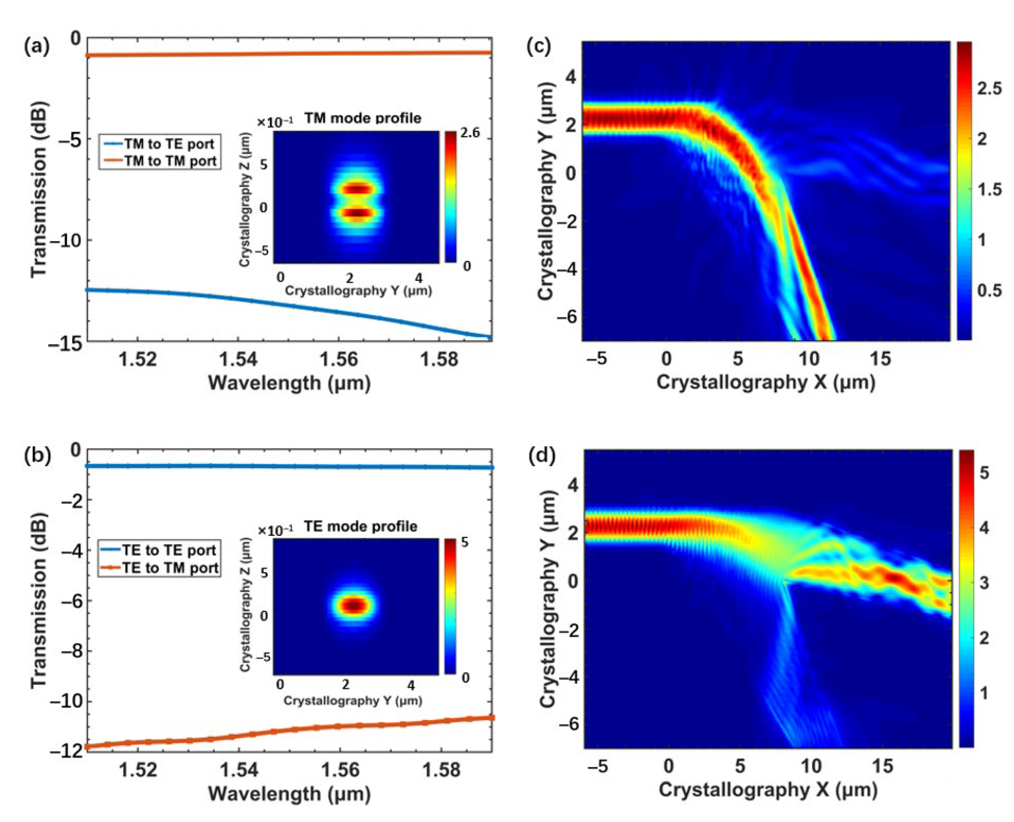
3. Results and Discussion

To verify the viability and reasonability of our model, the device performance was simulated via three-dimensional finite-difference-time-domain (3D FDTD) simulation, utilizing the Lumerical FDTD Solutions 2020 R2.4® software. The input and output ports were set as 2-μm-wide waveguides and the maximum meshing step was set as 10 nm. A DFT monitor was placed 8 μm behind the output ports to obtain the field strength distribution. Figure 4a,b shows the simulated light propagation in the designed PBS when the mixed input light is emitted from the input port of the device. It can be clearly seen from the figure that the incident light with a mixture of the TE mode and TM mode is introduced into the PBS element through the left port, and as light propagates along the x-axis inside the device, the separating distance of different polarizations increases, resulting in a large distance difference along the y-axis. The light of different polarization modes ultimately focuses on the different output ports’ efficiency. A quantitative evaluation of the performance of the metasurface PBS device is shown in Figure 4c,d, which demonstrates a high performance of the device over the entire 80 nm wavelength range. At a 1550 nm wavelength, the insertion loss (IL) of the TE mode reaches 0.706 dB, while the IL of the TM mode is 0.809 dB. The extinction ratio (ER) is defined as the ratio of the power of a matched mode to another mode in the corresponding output port. According to the results shown in the figure, the calculated ERs for the TE output port and TM port of the device are 12.59 dB and 10.76 dB at 1550 nm wavelength, respectively. It can be seen from the figure that when operating at shorter wavelengths, the output efficiency of the TE mode is relatively higher, while that of the TM mode performs the opposite. The reason is that the metasurface layer exhibits a relatively larger difference in the equivalent refractive index when operating at longer wavelengths, resulting in a stronger deflection effect, thus the propagation directions of the two modes are deflected by a larger angle in the device. A simulation shows that both the TM and TE modes have low ILs (<0.731 dB for TE mode and <0.873 dB for TM mode) and low ERs (10.5~15 dB) over a broad wavelength band of 80 nm, thereby covering the C-band (1530~1565 nm), which shows the potential of the device to be used together with the WDM on-chip system to further improve the link capacity.
Since manufacturing defects, which usually lead to the deterioration of the device performance, are unavoidable in practical applications, we simulated the device performance under different fabrication errors to verify whether the device has good tolerance. We first simulated the possible under-etching and over-etching conditions during the etching process, and the simulation results show that the device can tolerate a variation in etch depth of up to ±20 nm, as shown in Figure 5a–d. ILs of both polarization modes fall less than 0.34 dB from the peak value over the entire 80 nm width band, while the reduction of ERs is up to 2.95 dB. We noticed that, whether under-etched or over-etched, the separation efficiency of the device for TM-polarized light fluctuates greatly, while TE-polarized light is almost unaffected. This is consistent with our previous setup where the equivalent refractive index of the TE mode hardly varies with the structure of the metasurface layer.
To elucidate the tolerance of our device to small changes in device geometry, we simulated the device behavior under irregular etching conditions. Considering the outer proximity effect during the etching process, an etched shape close to a round hole is used to replace the ideal square etched air hole. The simulation results under this circumstance indicate that the device is robust to small geometry changes, as shown in Figure 6a,b, while ERs of both the TE and TM mode are above 10 dB, and ILs remain smaller than 1.07 dB over the entire 80 nm bandwidth from 1510 nm to 1590 nm. Considering that the metasurface layer of the device needs to be formed on a standard SOI, there is a high possibility of deviation in the layer from the ideal position. We simulated the device performance when the additional layer deviates from the ideal position by 1 μm toward the input port, as shown in Figure 6c,d. The results show that the separation function of the PBS device is still efficient, with low ILs (<1.36 dB for TM mode, and <0.79 dB for TE mode) over the entire 80 nm bandwidth and fairly low ERs (>9 dB for TM mode and >11.5 dB for TE mode) in the C-band. The simulation results indicate that the metasurface PBS is suitable for future WDM and PDM communication applications in SOI platform.

4. Conclusions

We have demonstrated an ultra-compact polarization beam splitter utilizing a metasurface layer formed on SOI based on the physics-constrained DBS algorithm. The simulation shows that at 1550 nm, the insertion losses of the TE and TM modes are 0.706 dB and 0.809 dB, and the extinction ratios of the TE output port and TM output port are 12.59 dB and 10.76 dB, respectively. The low insertion loss (<0.731 dB for TE mode and <0.873 dB for TM mode) over a large wavelength range of 1510 nm to 1590 nm (covering the C-band) indicates that the device has a high performance under broadband inputs. Furthermore, our study demonstrates that the device has good tolerance to fabrication errors. We hope this novel device can be used as a highly-functional nanophotonic element for densely integrated PDM systems.

Author Contributions

Conceptualization, H.S.; Data curation, Z.L. and L.W. (Lu Wang); Formal analysis, L.W. (Lin Wang) and L.Z.; Investigation, R.T.; Methodology, H.S. and L.Z.; Resources, Y.W. and R.T.; Software, H.S., L.W. (Lin Wang) and Z.L.; Supervision, L.Z. and Y.W.; Writing—original draft, H.S.; Writing—review & editing, H.S., L.Z. and Y.W. All authors have read and agreed to the published version of the manuscript.

Funding

This research was funded by National Key R&D Program of China, grant number 2017YFA0206002, 2017YFA0403400.

Institutional Review Board Statement

Not applicable.

Informed Consent Statement

Not applicable.

Data Availability Statement

Not applicable.

Conflicts of Interest

The authors declare no conflict of interest.

References

  1. Cheben, P.; Halir, R.; Schmid, J.H.; Atwater, H.A.; Smith, D.R. Subwavelength integrated photonics. Nature 2018, 560, 565–572. [Google Scholar] [CrossRef] [PubMed]
  2. Siew, S.Y.; Li, B.; Gao, F.; Zheng, H.Y.; Zhang, W.; Guo, P.; Xie, S.W.; Song, A.; Dong, B.; Luo, L.W.; et al. Review of Silicon Photonics Technology and Platform Development. J. Light. Technol. 2021, 39, 4374–4389. [Google Scholar] [CrossRef]
  3. Thylén, L.; Wosinski, L. Integrated photonics in the 21st century. Photonics Res. 2014, 2, 75–81. [Google Scholar] [CrossRef]
  4. Lim, A.E.; Song, J.; Fang, Q.; Li, C.; Tu, X.; Duan, N.; Chen, K.K.; Tern, R.P.; Liow, T. Review of Silicon Photonics Foundry Efforts. IEEE J. Sel. Top. Quantum Electron. 2014, 20, 405–416. [Google Scholar] [CrossRef]
  5. Aydin, K. Nanostructured silicon success. Nat. Photonics 2015, 9, 353–355. [Google Scholar] [CrossRef]
  6. Cheng, Z.; Wang, J.; Yang, Z.; Zhu, L.; Yang, Y.; Huang, Y.; Ren, X. Sub-wavelength grating assisted mode order converter on the SOI substrate. Opt. Express 2019, 27, 34434–34441. [Google Scholar] [CrossRef]
  7. Zhang, F.; Ruan, X.; Zhu, Y.; Chen, Z.; Qiu, X.; Yang, F.; Li, K.; Li, Y. Compact polarization diversity Kramers-Kronig coherent receiver on silicon chip. Opt. Express 2019, 27, 23654–23660. [Google Scholar] [CrossRef] [Green Version]
  8. Bogaerts, W.; Chrostowski, L. Silicon Photonics Circuit Design: Methods, Tools and Challenges. Laser Photonics Rev. 2018, 12, 1700237. [Google Scholar] [CrossRef] [Green Version]
  9. Won, R.; Paniccia, M. Integrating silicon photonics. Nat. Photonics 2010, 4, 498–499. [Google Scholar] [CrossRef]
  10. Shen, B.; Wang, P.; Polson, R.; Menon, R. An integrated-nanophotonics polarization beamsplitter with 2.4 × 2.4 μm2 footprint. Nat. Photonics 2015, 9, 378–382. [Google Scholar] [CrossRef]
  11. Tosi, M.; Fasciszewki, A.; Bulus Rossini, L.; Costanzo Caso, P. Silicon Nitride Polarization Beam Splitters: A Review. IET Optoelectron. 2020, 14, 120–124. [Google Scholar] [CrossRef]
  12. Yuan, W.Q.; Kojima, K.; Wang, B.N.; Koike-Akino, T.; Parsons, K.; Nishikawa, S.; Yagyu, E. Mode-evolution-based polarization rotator-splitter design via simple fabrication process. Opt. Express 2012, 20, 10163–10169. [Google Scholar] [CrossRef] [PubMed] [Green Version]
  13. Dai, D.; Li, C.; Wang, S.; Wu, H.; Shi, Y.; Wu, Z.; Gao, S.; Dai, T.; Yu, H.; Tsang, H.-K. 10-Channel Mode (de)multiplexer with Dual Polarizations. Laser Photonics Rev. 2018, 12, 1700109. [Google Scholar] [CrossRef]
  14. Zhang, Y.; He, Y.; Zhu, Q.; Jiang, X.; Guo, X.; Qiu, C.; Su, Y. On-chip silicon polarization and mode handling devices. Front. Optoelectron. 2018, 11, 77–91. [Google Scholar] [CrossRef]
  15. Chang, L.M.; Liu, L.; Gong, Y.H.; Tan, M.Q.; Yu, Y.D.; Li, Z.Y. Polarization-independent directional coupler and polarization beam splitter based on asymmetric cross-slot waveguides. Appl. Opt. 2018, 57, 678–683. [Google Scholar] [CrossRef] [PubMed]
  16. Cai, H.; Boynton, N.; Lentine, A.; Pomerene, A.; Trotter, D.; Starbuck, A.; Davids, P.; DeRose, C. An adiabatic/diabatic polarization beam splitter. In Proceedings of the 2016 IEEE Optical Interconnects Conference (OI), San Diego, CA, USA, 9–11 May 2016; pp. 102–103. [Google Scholar]
  17. Huang, J.; Yang, J.; Chen, D.; He, X.; Han, Y.; Zhang, J.; Zhang, Z. Ultra-compact broadband polarization beam splitter with strong expansibility. Photonics Res. 2018, 6, 574. [Google Scholar] [CrossRef]
  18. Bhandari, B.; Im, C.-S.; Sapkota, O.; Lee, S.-S. Highly efficient broadband silicon nitride polarization beam splitter incorporating serially cascaded asymmetric directional couplers. Opt. Lett. 2020, 45, 5974–5977. [Google Scholar] [CrossRef]
  19. Shi, X.; Zhang, J.; Fan, W.; Lu, Y.; Peng, N.; Rottwitt, K.; Ou, H. Compact low-birefringence polarization beam splitter using vertical-dual-slot waveguides in silicon carbide integrated platforms. Photonics Res. 2021, 10, A8–A13. [Google Scholar] [CrossRef]
  20. Zhang, J.; Shi, X.; Zhang, Z.; Guo, K.; Yang, J. Ultra-compact, efficient and high-polarization-extinction-ratio polarization beam splitters based on photonic anisotropic metamaterials. Opt. Express 2021, 30, 538–549. [Google Scholar] [CrossRef]
  21. Guan, X.; Yin, S.; Qiu, H.; Wang, Z.; Dai, D. On-Chip Silicon Switchable polarization beam splitter. Opt. Lett. 2022, 47, 961–964. [Google Scholar]
  22. Huang, Y.Y.; Xu, G.Y.; Ho, S.T. An ultracompact optical mode order converter. IEEE Photonics Technol. Lett. 2006, 18, 2281–2283. [Google Scholar] [CrossRef]
  23. Lu, Z.; Yun, H.; Wang, Y.; Chen, Z.; Zhang, F.; Jaeger, N.A.F.; Chrostowski, L. Broadband silicon photonic directional coupler using asymmetric-waveguide based phase control. Opt. Express 2015, 23, 3795–3808. [Google Scholar] [CrossRef] [PubMed]
  24. Lu, M.F.; Liao, S.M.; Huang, Y.T. Ultracompact photonic crystal polarization beam splitter based on multimode interference. Appl. Opt. 2010, 49, 724–731. [Google Scholar] [CrossRef] [PubMed]
  25. Liang, H.; Soref, R.; Mu, J. Compact polarization splitter based on a silicon angled multimode interferometer structure. Appl. Opt. 2019, 58, 4070–4074. [Google Scholar] [CrossRef] [PubMed]
  26. Xu, D.-X.; Densmore, A.; Waldron, P.; Lapointe, J.; Post, E.; Delâge, A.; Janz, S.; Cheben, P.; Schmid, J.H.; Lamontagne, B. High bandwidth SOI photonic wire ring resonators using MMI couplers. Opt. Express 2007, 15, 3149–3155. [Google Scholar] [CrossRef] [PubMed]
  27. Ma, H.; Huang, J.; Zhang, K.; Yang, J. Ultra-compact and efficient 1 × 2 mode converters based on rotatable direct-binary-search algorithm. Opt. Express 2020, 28, 17010–17019. [Google Scholar] [CrossRef] [PubMed]
  28. Zheng, Z.H.; Chen, Y.; Chen, H.Y.; Chen, J.H. Ultra-compact reconfigurable device for mode conversion and dual-mode DPSK demodulation via inverse design. Opt. Express 2021, 29, 17718–17725. [Google Scholar] [CrossRef]
  29. Dong, Z.; Qiu, J.; Chen, Y.; Liu, C.; Guo, H.; Zhang, W.; He, Z.; Wu, J. Ultra-compact X-shaped waveguide crossings with flexible angles based on inverse design. Opt. Express 2021, 29, 19715–19726. [Google Scholar] [CrossRef]
  30. Chang, W.; Xu, S.; Cheng, M.; Liu, D.; Zhang, M. Inverse design of a single-step-etched ultracompact silicon polarization rotator. Opt. Express 2020, 28, 28343–28351. [Google Scholar] [CrossRef]
  31. Xu, X.; Li, Y.; Huang, W. Inverse design of the MMI power splitter by asynchronous double deep Q-learning. Opt. Express 2021, 29, 35951–35964. [Google Scholar] [CrossRef]
  32. Wei, H.M.; Callewaert, F.; Hadibrata, W.; Velev, V.; Liu, Z.Z.; Kumar, P.; Aydin, K.; Krishnaswamy, S. Two-Photon Direct Laser Writing of Inverse-Designed Free-Form Near-Infrared Polarization Beamsplitter. Adv. Opt. Mater. 2019, 7, 1900513. [Google Scholar] [CrossRef]
  33. Frellsen, L.; Ding, Y.; Sigmund, O.; Frandsen, L. Topology optimized mode multiplexing in silicon-on-insulator photonic wire waveguides. Opt. Express 2016, 24, 16866–16873. [Google Scholar] [CrossRef] [PubMed] [Green Version]
  34. Phan, T.; Sell, D.; Wang, E.W.; Doshay, S.; Edee, K.; Yang, J.; Fan, J.A. High-efficiency, large-area, topology-optimized metasurfaces. Light Sci. Appl. 2019, 8, 48. [Google Scholar] [CrossRef] [PubMed] [Green Version]
  35. Augenstein, Y.; Rockstuhl, C. Inverse Design of Nanophotonic Devices with Structural Integrity. ACS Photonics 2020, 7, 2190–2196. [Google Scholar] [CrossRef]
  36. Meng, Y.; Chen, Y.; Lu, L.; Ding, Y.; Cusano, A.; Fan, J.A.; Hu, Q.; Wang, K.; Xie, Z.; Liu, Z.; et al. Optical meta-waveguides for integrated photonics and beyond. Light Sci. Appl. 2021, 10, 235. [Google Scholar] [CrossRef] [PubMed]
  37. Sun, L.; Zhang, Y.; He, Y.; Wang, H.; Su, Y. Subwavelength structured silicon waveguides and photonic devices. Nanophotonics 2020, 9, 1321–1340. [Google Scholar] [CrossRef]
  38. Sun, Y.; Zhang, L.; Xia, H.; Cao, S.; Wang, L.; Yang, S.; Wu, Y.; Tai, R. Integrated silicon metasurface polarization beam splitter on a standard SOI substrate. Optik 2021, 227, 166096. [Google Scholar]
  39. Lipson, M. Guiding, modulating, and emitting light on Silicon - Challenges and opportunities. J. Light. Technol. 2005, 23, 4222–4238. [Google Scholar] [CrossRef]
  40. Li, S.; Zhang, Z.; Wang, J.; He, X. Design of conformal lens by drilling holes materials using quasi-conformal transformation optics. Opt. Express 2014, 22, 25455–25465. [Google Scholar] [CrossRef]
  41. Seldowitz, M.A.; Allebach, J.P.; Sweeney, D.W. Synthesis of digital holograms by direct binary search. Appl. Opt. 1987, 26, 2788–2798. [Google Scholar] [CrossRef]
Figure 1. Schematic of the metasurface polarization beam splitter. (a) Top view of the proposed PBS. Inset: the zoom-in top view of a single pixel in the metasurface layer. (b) Cross-section of the area marked by the red line, which indicates the structural form of metasurface built on the standard SOI. The topmost metasurface layer can be divided into a series of small pixels of 80 × 80 nm2, each of which has two optional modes: etched air hole or silicon. (c) The metasurface structure, in which the light area represents the doped air, and the dark area represents the 120 nm thick silicon structure.
Applsci 12 10064 g001
Figure 2. (a) The normalized effective refractive indices for the TE and TM mode as a function of the thickness of the metasurface layer. (b) Relationship between the number of etched grids and the normalized effective refractive indices for the TE and TM mode, thereby matching the typical cell structures of each density mode. (c) Index profile of the TM mode at the initial time and (d) after optimization.
Applsci 12 10064 g002
Figure 3. Design pipeline for the metasurface layer.
Applsci 12 10064 g003
Figure 4. The simulated normalized transmission spectra with detected mode profiles for (a) TM mode and (b) TE mode. E-field profiles of the propagation along the device for (c) TM mode and (d) TE mode.
Applsci 12 10064 g004
Figure 5. (a) Device performance when suffering 20 nm over-etch for TE mode and (b) TM mode. (c) Device performance when suffering 20 nm under-etch for TE mode and (d) TM mode.
Applsci 12 10064 g005
Figure 6. (a) Device performance under irregular etching conditions for TE mode and (b) TM mode. (c) Device performance when the metasurface layer suffers a 1 μm deviation for TE mode and (d) TM mode.
Applsci 12 10064 g006
Publisher’s Note: MDPI stays neutral with regard to jurisdictional claims in published maps and institutional affiliations.

