
Recent Progress in On-Chip Erbium-Based Light Sources
Abstract
:Featured Application
Abstract
1. Introduction
1.1. Epitaxial III-V Light Sources
1.2. Heterogeneous III-V Light Sources
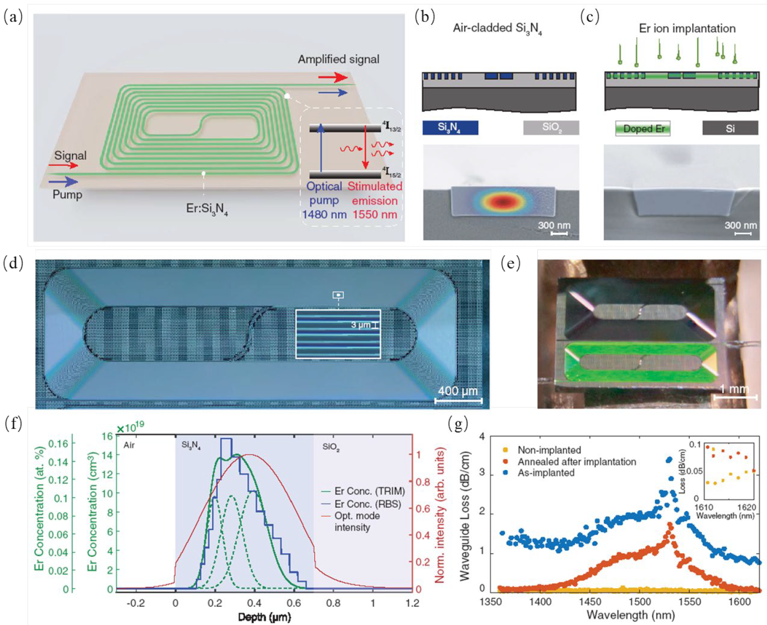
1.3. Er-Based Light Sources
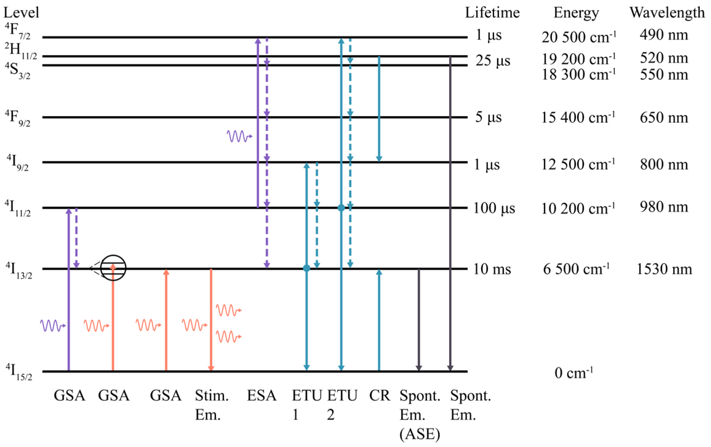
2. Electronic Energy Level Structure and Amplification in Er-Based Medium
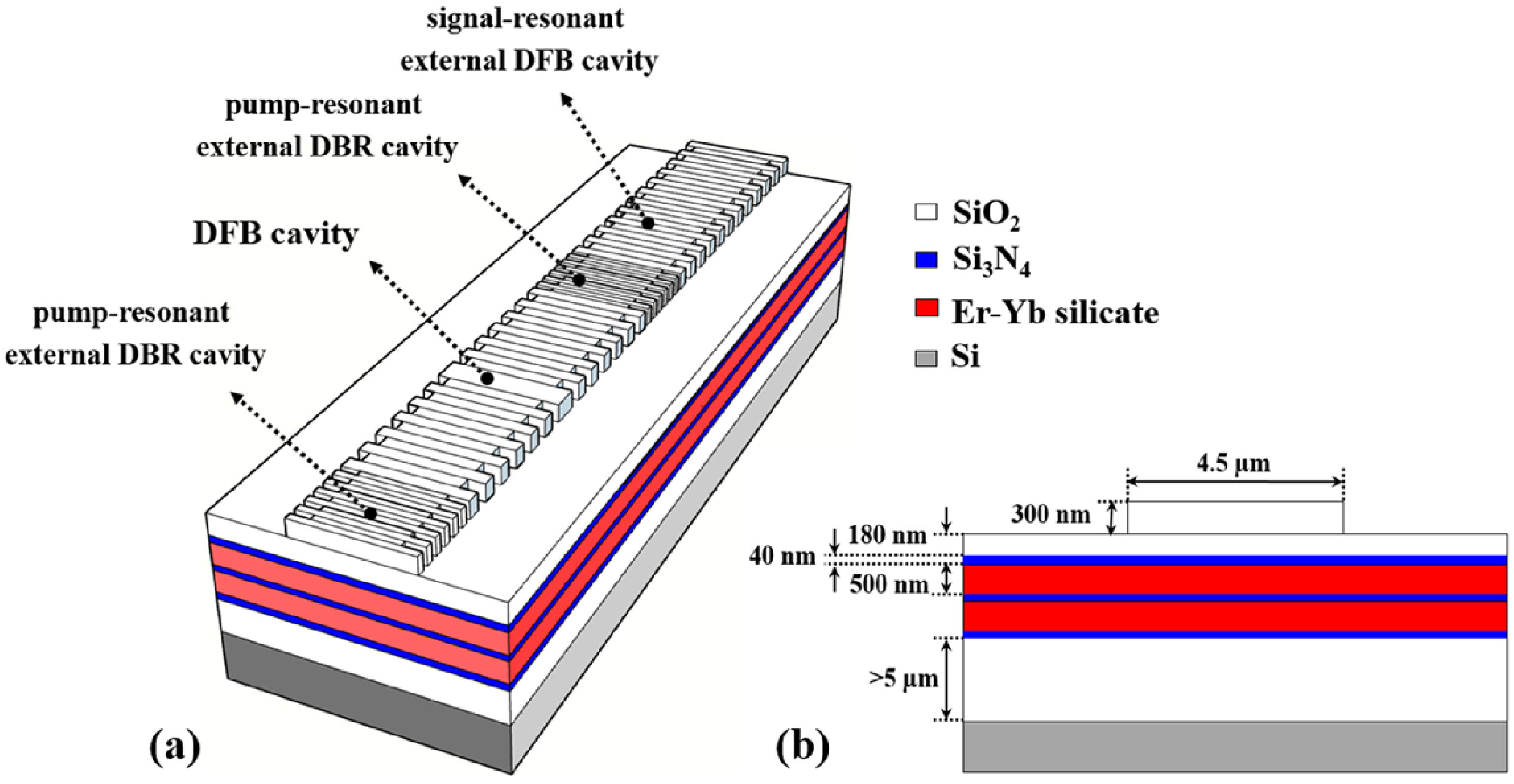
3. Gain Medium Based on Different Host Materials
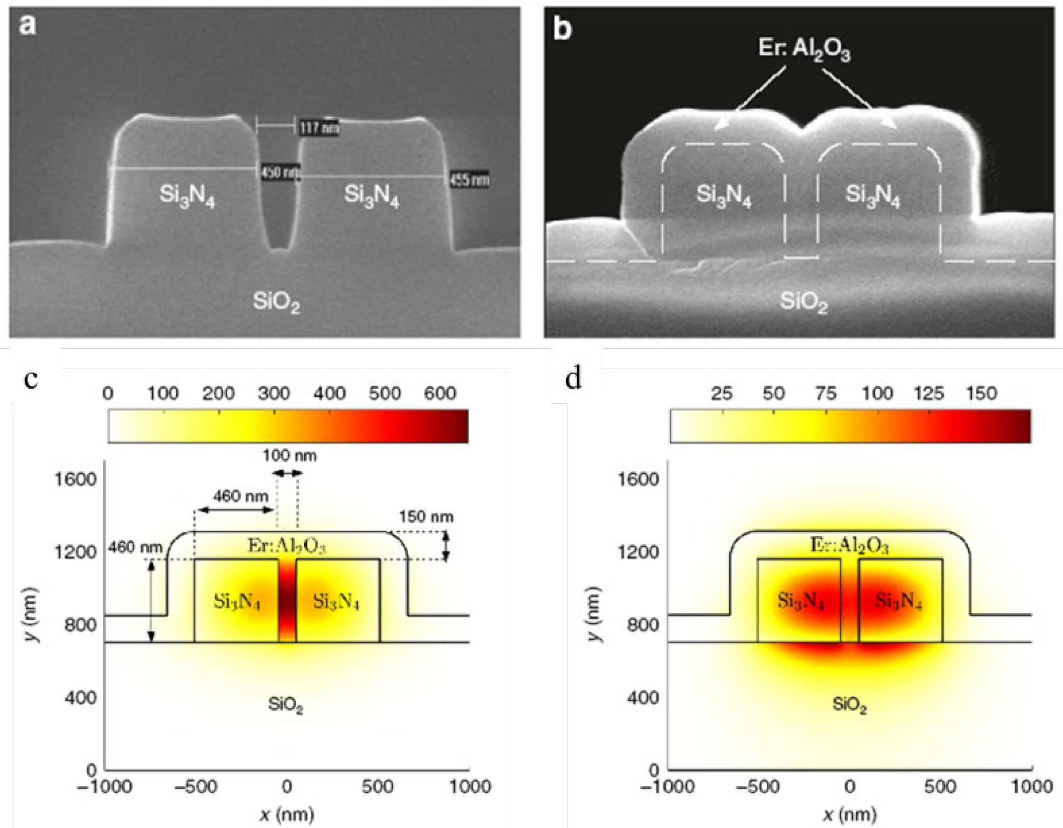
3.1. Er-Doped Al2O3
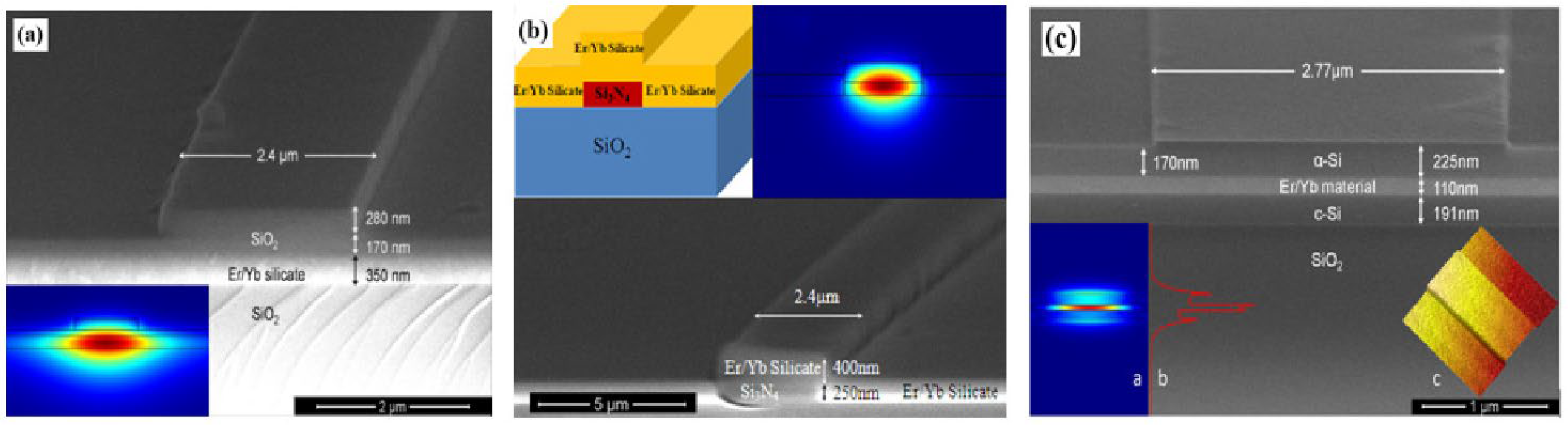
3.2. Er Silicate
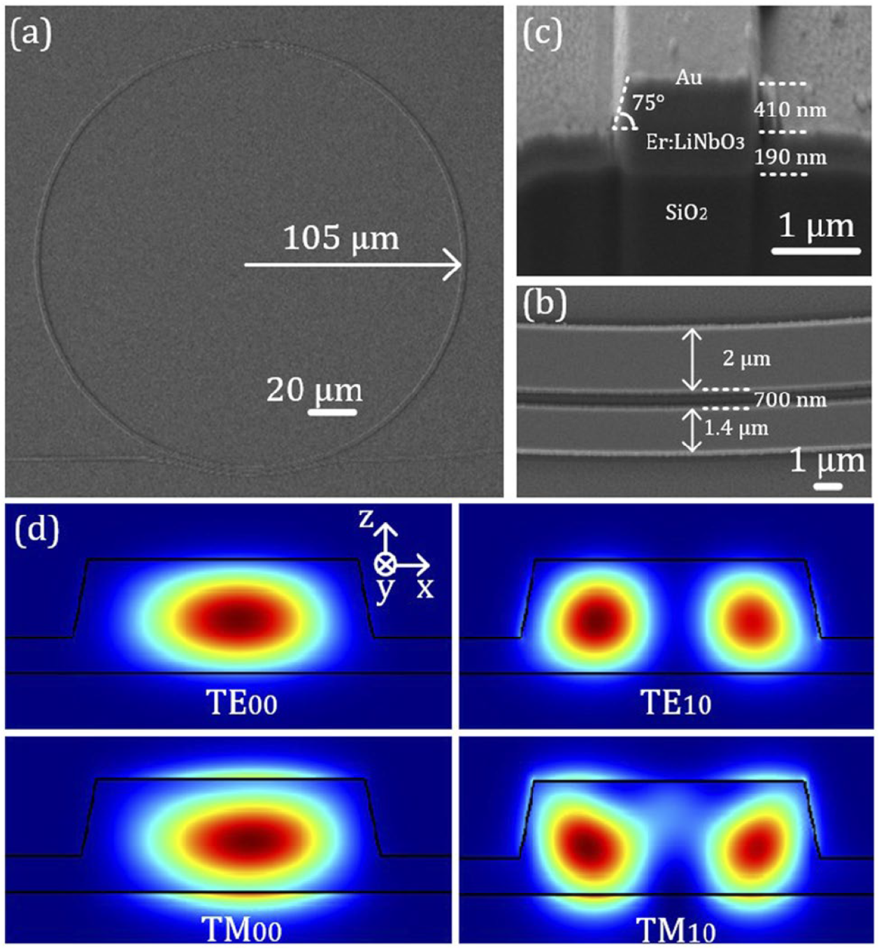
3.3. Other Er-Doped Host Material
4. Discussion
5. Conclusions
Author Contributions
Funding
Institutional Review Board Statement
Informed Consent Statement
Data Availability Statement
Conflicts of Interest
References
- Moore, G.E. Cramming more components onto integrated circuits. Electronics 1965, 38, 114–117. [Google Scholar] [CrossRef]
- Waldrop, M.M. More than Moore. Nature 2016, 530, 145–147. [Google Scholar]
- Soref, R.A. Silicon-based optoelectronics. Proc. IEEE 1993, 81, 1687–1706. [Google Scholar] [CrossRef]
- Margalit, N.; Xiang, C.; Bowers, S.M.; Bjorlin, A.; Blum, R.; Bowers, J.E. Perspective on the future of silicon photonics and electronics. Appl. Phys. Lett. 2021, 118, 220501. [Google Scholar] [CrossRef]
- Bogaerts, W.; Perez, D.; Capmany, J.; Miller, D.; Poon, J.; Englund, D.; Morichetti, F.; Melloni, A. Programmable photonic circuits. Nature 2020, 586, 207–216. [Google Scholar] [CrossRef] [PubMed]
- Bai, B.; Shu, H.; Wang, X.; Zou, W. Towards silicon photonic neural networks for artificial intelligence Sci. China Inform. Sci. 2020, 63, 160403. [Google Scholar] [CrossRef]
- Teklu, B.; Bina, M.; Paris, M.G.A. Noisy propagation of Gaussian states in optical media with finite bandwidth. Sci. Rep. 2022, 12, 11646. [Google Scholar] [CrossRef]
- Teklu, B. Continuous-variable entanglement dynamics in Lorentzian environment. Phys. Lett. A 2022, 432, 128022. [Google Scholar] [CrossRef]
- Shen, B.; Shu, H.; Zhou, L.; Wang, X. A design method for high fabrication tolerance integrated optical mode multiplexer. Sci. China Inform. Sci. 2020, 63, 160409. [Google Scholar] [CrossRef]
- Reed, G.T.; Mashanovich, G.; Gardes, F.Y.; Thomson, D.J. Silicon optical modulators. Nat. Photonics 2010, 4, 518–526. [Google Scholar] [CrossRef] [Green Version]
- Michel, J.; Liu, J.L.; Kimerling, L.C. High-performance Ge-on-Si photodetectors. Nat. Photonics 2010, 4, 527–534. [Google Scholar] [CrossRef]
- Shu, H.; Chang, L.; Tao, Y.; Shen, B.; Xie, W.; Jin, M.; Netherton, A.; Tao, Z.; Zhang, X.; Chen, R.; et al. Microcomb-driven silicon photonic systems. Nature 2022, 605, 457–463. [Google Scholar] [CrossRef] [PubMed]
- Morichetti, F.; Milanizadeh, M.; Petrini, M.; Zanetto, F.; Ferrari, G.; Aguiar, D.O.; Guglielmi, E.; Sampietro, M.; Meiioni, A. Polarization-transparent silicon photonic add-drop multiplexer with wideband hitless tuneability. Nat. Commun. 2021, 12, 4324. [Google Scholar] [CrossRef] [PubMed]
- Liang, D.; Bowers, J.E. Recent progress in lasers on silicon. Nat. Photonics 2010, 4, 511–517. [Google Scholar] [CrossRef]
- Kawanami, H. Heteroepitaxial technologies of III–V on Si. Sol. Energy Mater. Sol. C 2001, 66, 479–486. [Google Scholar] [CrossRef]
- Xie, Y.H.; Wang, K.L.; Kao, Y.C. An investigation on surface conditions for Si molecular beam epitaxial (MBE) growth. J. Vac. Sci. Technol. A 1985, 3, 1035. [Google Scholar] [CrossRef]
- Samonji, K.; Yonezu, H.; Takagi, Y.; Iwaki, K.; Ohshima, N.; Shin, J.K.; Pak, K. Reduction of threading dislocation density in InP-on-Si heteroepitaxy with strained short-period superlattices. Appl. Phys. Lett. 1996, 69, 100–102. [Google Scholar] [CrossRef]
- Yamaguchi, M.; Sugo, M.; Itoh, Y. Misfit stress dependence of dislocation density reduction in GaAs films on Si substrates grown by strained-layer superlattices. Appl. Phys. Lett. 1989, 54, 2568–2570. [Google Scholar] [CrossRef]
- Nozawa, K.; Horikoshi, Y. Low threading dislocation density GaAs on Si(100) with InGaAs/GaAs strained-layer superlattice grown by migration-enhanced epitaxy. Jpn. J. Appl. Phys. 1991, 30, 668–671. [Google Scholar] [CrossRef]
- Yamaichi, E.; Ueda, T.; Gao, Q.; Yamagishi, C.; Akiyama, M. Method to obtain low-dislocation-density regions by patterning with SiO2 on GaAs/Si followed by annealing. Jpn. J. Appl. Phys. 1994, 33, 1442–1444. [Google Scholar] [CrossRef]
- Linder, K.K.; Phillips, J.; Qasaimeh, O.; Liu, X.F.; Krishna, S.; Bhattacharya, P. Self-organized In0.4Ga0.6As quantum-dot lasers grown on Si substrates. Appl. Phys. Lett. 1999, 74, 1355. [Google Scholar] [CrossRef]
- Wang, T.; Liu, H.; Lee, A.; Pozzi, F.; Seeds, A. 1.3-μm InAs/GaAs quantum-dot lasers monolithically grown on Si substrates. Opt. Express 2011, 19, 11381–11386. [Google Scholar] [CrossRef] [PubMed]
- Kryzhanovskaya, N.; Moiseev, E.; Polubavkina, Y.; Maximov, M.; Kulagina, M.; Troshkov, S.; Zadiranov, Y.; Guseva, Y.; Lipovskii, A.; Tang, M.; et al. Heat-sink free CW operation of injection microdisk lasers grown on Si substrate with emission wavelength beyond 1.3 μm. Opt. Lett. 2017, 42, 3319–3322. [Google Scholar] [CrossRef] [PubMed] [Green Version]
- Wang, Y.; Chen, S.; Yu, Y.; Zhou, L.; Liu, L.; Yang, C.; Liao, M.; Tang, M.; Liu, Z.; Wu, J.; et al. Monolithic quantum-dot distributed feedback laser array on silicon. Optica 2018, 5, 528–533. [Google Scholar] [CrossRef]
- Wan, Y.; Zhang, S.; Norman, J.C.; Kennedy, M.J.; He, W.; Liu, S.; Xiang, C.; Shang, C.; He, J.J.; Gossard, A.C.; et al. Tunable quantum dot lasers grown directly on silicon. Optica 2019, 6, 1394–1400. [Google Scholar] [CrossRef]
- Wang, Y.; Norman, J.; Liu, S.; Liu, A.; Bowers, J.E. Quantum dot lasers and amplifiers on silicon: Recent advances and future developments. IEEE Nanotechnol. Mag. 2021, 15, 8–22. [Google Scholar]
- Liang, D.; Bowers, J.E. Recent progress in heterogeneous III-V-on-silicon photonic integration. Light Adv. Manuf. 2021, 2, 5. [Google Scholar] [CrossRef]
- Bao, S.; Wang, Y.; Lina, K.; Zhang, L.; Wang, B.; Sasangka, W.A.; Lee, K.E.K.; Chua, S.J.; Michel, J.; Fitzgerald, E.; et al. A review of silicon-based wafer bonding processes, an approach to realize the monolithic integration of Si-CMOS and III–V-on-Si wafers. J. Semicond. 2021, 42, 023106. [Google Scholar] [CrossRef]
- Park, H.; Fang, A.W.; Kodama, S.; Bowers, J.E. Hybrid silicon evanescent laser fabricated with a silicon waveguide and III-V offset quantum wells. Opt. Express 2005, 13, 9460–9464. [Google Scholar] [CrossRef] [Green Version]
- Fang, A.W.; Park, H.; Cohen, O.; Jones, R.; Paniccia, M.J.; Bowers, J.E. Electrically pumped hybrid AlGaInAs-silicon evanescent laser. Opt. Express 2006, 14, 9203–9210. [Google Scholar] [CrossRef]
- Santis, C.T.; Vilenchik, Y.; Yariv, A.; Satyan, N.; Rakulijic, G. Sub-kHz quantum linewidth semiconductor laser on silicon chip. In Proceedings of the 2015 Conference on Lasers and Electro-Optics (CLEO), San Jose, CA, USA, 10–15 May 2015; pp. 1–2. [Google Scholar]
- Thiessen, T.; Mak, J.C.C.; Fonseca, J.D.; Ribaud, K.; Jany, C.; Poon, J.K.S.; Menezo, S. Back-side-on-BOX heterogeneously integrated III-V-on-silicon O-band distributed feedback lasers. J. Lightwave Technol. 2020, 38, 3000–3006. [Google Scholar] [CrossRef]
- Yu, H.; Doussiere, P.; Patel, D.; Lin, W.; Hemyari, K.; Park, J.; Jan, C.; Herrick, R.; Hoshino, I.; Busselle, L.; et al. 400Gbps Fully Integrated DR4 Silicon Photonics Transmitter for Data Center Applications. In Proceedings of the 2020 Optical Fiber Communications Conference and Exhibition (OFC), San Diego, CA, USA, 8–12 March 2020. paper T3H.6. [Google Scholar]
- Li, N.; Su, Z.; Magden, E.S.; Callahan, P.T.; Shtyrkova, K.; Xin, M.; Ruocco, A.; Baiocco, C.; Ippen, E.P.; Kartner, F.X.; et al. High-power thulium lasers on a silicon photonics platform. Opt. Lett. 2017, 42, 1181–1184. [Google Scholar] [CrossRef] [PubMed]
- Li, N.; Magden, E.S.; Su, Z.; Singh, N.; Ruocco, A.; Xin, M.; Byrd, M.; Callahan, P.T.; Bradley, J.D.B.; Baiocco, C.; et al. Broadband 2-μm emission on silicon chips: Monolithically integrated Holmium lasers. Opt. Express 2018, 26, 2220–2230. [Google Scholar] [CrossRef] [PubMed]
- Li, N.; Vermeulen, D.; Su, Z.; Magden, E.S.; Xin, M.; Singh, N.; Ruocco, A.; Notaros, J.; Poulton, C.V.; Timurdogan, E.; et al. Monolithically integrated Er-doped tunable laser on a CMOS-compatible silicon photonics platform. Opt. Express 2018, 26, 16200–16211. [Google Scholar] [CrossRef] [PubMed] [Green Version]
- Poole, S.B.; Payne, D.N.; Fermann, M.E. Fabrication of low-loss optical fibers containing rare-earth ions. Electron. Lett. 1985, 21, 737–738. [Google Scholar] [CrossRef] [Green Version]
- Bradley, J.D.B.; Pollnau, M. Erbium-doped integrated waveguide amplifiers and lasers. Laser Photonics Rev. 2011, 5, 368–403. [Google Scholar] [CrossRef]
- Sun, H.; Yin, L.; Liu, Z.; Zheng, Y.; Fan, F.; Zhao, S.; Feng, X.; Li, Y.; Ning, N.Z. Giant optical gain in a single-crystal erbium chloride silicate nanowire. Nat. Photonics 2017, 11, 589–593. [Google Scholar] [CrossRef]
- Ronn, J.; Zhang, W.; Autere, A.; Leroux, X.; Pakarinen, L.; Alonso-Ramos, C.; Saynatjoki, A.; Lipsanen, H.; Vivien, L.; Cassan, E.; et al. Ultra-high on-chip optical gain in erbium-based hybrid slot waveguides. Nat. Commun. 2019, 10, 432. [Google Scholar] [CrossRef] [Green Version]
- Liu, Y.; Qiu, Z.; Ji, X.; Lukashchuk, A.; He, J.; Riemensberger, J.; Hafermann, M.; Wang, R.N.; Liu, J.; Ronning, C.; et al. A photonic integrated circuit–based erbium-doped amplifier. Sciences 2022, 376, 1309–1313. [Google Scholar] [CrossRef]
- Wang, X.; Zhou, P.; He, Y.; Zhou, Z. Erbium silicate compound optical waveguide amplifier and laser. Opt. Mater. Express 2018, 8, 2970–2990. [Google Scholar] [CrossRef]
- Hoven, G.N.; Snoeks, E.; Polman, A.; Uffelen, J.W.M.; Oei, Y.S.; Smit, M.K. Photoluminescence characterization of Er-implanted Al2O3 films. Appl. Phys. Lett. 1993, 62, 3065. [Google Scholar] [CrossRef] [Green Version]
- Bradley, J.D.B.; Agazzi, L.; Geskus, D.; Worhoff, A.K.; Pollnau, M. Gain bandwidth of 80 nm and 2 dB/cm peak gain in Al2O3:Er3+ optical amplifiers on silicon. J. Opt. Soc. Am. B 2010, 27, 187–196. [Google Scholar] [CrossRef]
- Hosseini, E.S.; Bradley, J.D.B.; Sun, J.; Leake, G.; Adam, T.N.; Coolbaugh, D.D.; Watts, M.R. CMOS-compatible 75 mW Er-doped distributed feedback laser. Opt. Lett. 2014, 39, 3106–3109. [Google Scholar] [CrossRef] [PubMed] [Green Version]
- Sun, J.; Hosseini, E.S.; Bradley, J.D.B.; Adam, T.N.; Leake, G.; Coolbaugh, D.; Watts, M.R. Uniformly spaced λ/4-shifted Bragg grating array with wafer-scale CMOS-compatible process. Opt. Lett. 2013, 38, 4002–4004. [Google Scholar] [CrossRef] [PubMed] [Green Version]
- Bradley, J.D.B.; Hosseini, E.S.; Su, Z.; Adam, T.N.; Leake, G.; Coolbaugh, D.; Watts, M.R. Monolithic erbium- and ytterbium-doped microring lasers on silicon chips. Opt. Express 2014, 22, 12226–12237. [Google Scholar] [CrossRef] [Green Version]
- Singh, G.; Bradley, J.D.B.; Li, N.; Magden, E.S.; Moresco, M.; Adam, T.N.; Leake, G.; Coolbaugh, D.; Watts, M.R. Resonant pumped Er-doped waveguide lasers using distributed Bragg reflector cavities. Opt. Lett. 2016, 41, 1189–1192. [Google Scholar] [CrossRef]
- Mu, J.; Dijkstra, M.; Korterik, J.; Offerhaus, H.; Garcia-Blaco, S.M. High-gain waveguide amplifiers in Si3N4 technology via double-layer monolithic integration. Photonics Res. 2020, 8, 1634–1641. [Google Scholar] [CrossRef]
- Wang, X.J.; Nakajima, T.; Isshiki, H.; Kimura, T. Fabrication and characterization of Er silicates on SiO2/Si substrates. Appl. Phys. Lett. 2009, 95, 041906. [Google Scholar] [CrossRef]
- Wang, X.J.; Wang, B.; Wang, L.; Guo, R.M.; Isshiki, H.; Kimura, T.; Zhou, Z. Extraordinary infrared photoluminescence efficiency of Er0.1Yb1.9SiO5 films on SiO2/Si substrates. Appl. Phys. Lett. 2011, 98, 071903. [Google Scholar] [CrossRef] [Green Version]
- Wang, X.J.; Yuan, G.; Isshiki, H.; Kimura, T.; Zhou, Z. Photoluminescence enhancement and high gain amplification of ErxY2-xSiO5 waveguide. Appl. Phys. Lett. 2010, 108, 013506. [Google Scholar] [CrossRef]
- Cardile, P.; Miritello, M.; Priolo, F. Energy transfer mechanisms in Er-Yb-Y disilicate thin films. Appl. Phys. Lett. 2012, 100, 251913. [Google Scholar] [CrossRef]
- Wang, B.; Guo, R.; Wang, X.; Wang, L.; Yin, B.; Zhou, Z. Large electroluminescence excitation cross section and strong potential gain of Er in ErYb silicate. J. Appl. Phys. 2013, 113, 103108. [Google Scholar] [CrossRef]
- Zhou, P.; Wang, X.; He, Y.; Wu, Z.; Du, J.; Fu, E. Effect of deposition mechanisms on the infrared photoluminescence of erbium-ytterbium silicate films under different sputtering methods. J. Appl. Phys. 2019, 125, 175114. [Google Scholar] [CrossRef]
- Isshiki, H.; Dood, M.J.A.; Polman, A.; Kimura, T. Self-assembled infrared-luminescent Er-Si-O crystallites on silicon. Appl. Phys. Lett. 2004, 85, 4343. [Google Scholar] [CrossRef] [Green Version]
- Savio, R.L.; Miritello, M.; Cardile, P.; Priolo, F. Concentration dependence of the Er3+ visible and infrared luminescence in Y2−xErxO3 thin films on Si. J. Appl. Phys. 2009, 106, 043510. [Google Scholar] [CrossRef]
- Savio, R.L.; Miritello, M.; Iacona, F.; Piro, A.M.; Grimaldi, M.G.; Priolo, F. Thermal evolution of Er silicate thin films grown by rf magnetron sputtering. J. Phys. Condens. Matter 2008, 20, 454218. [Google Scholar] [CrossRef]
- Wang, B.; Zhou, P.Q.; Wang, X.J.; He, Y.D. A low-fabrication-temperature, high-gain chip-scale waveguide amplifier. Sci. China Inform. Sci. 2022, 65, 162405. [Google Scholar] [CrossRef]
- Guo, R.; Wang, X.; Zang, K.; Wang, B.; Wang, L.; Gao, L.; Zhou, Z. Optical amplification in Er/Yb silicate strip loaded waveguide. Appl. Phys. Lett. 2011, 99, 161115. [Google Scholar] [CrossRef] [Green Version]
- Wang, L.; Guo, R.; Wang, B.; Wang, X.; Zhou, Z. Hybrid Si3N4-Er/Yb Silicate Waveguides for Amplifier Application. IEEE Photonic Tech. L. 2011, 24, 900–902. [Google Scholar] [CrossRef]
- Guo, R.; Wang, B.; Wang, X.; Wang, L.; Jiang, L.; Zhou, Z. Optical amplification in Er/Yb silicate slot waveguide. Opt. Lett. 2012, 37, 1427–1429. [Google Scholar] [CrossRef] [Green Version]
- Zhou, P.; Wang, X.; He, Y. A sub-kHz narrow-linewidth, and hundred-mW high-output-power silicon-based Er silicate laser with hybrid pump and signal co-resonant cavity. IEEE Photonics J. 2020, 12, 1500212. [Google Scholar] [CrossRef]
- Zhou, P.; Wang, X.; He, Y.; Zou, W. A high-power, high-efficiency hybrid silicon-based Er silicate-silicon nitride waveguide laser. IEEE J. Quantum Elect. 2020, 56, 110111. [Google Scholar] [CrossRef]
- Zhou, P.; Wang, B.; Wang, X.; Wang, B.; He, Y.; Bowers, J.E. Design of an on-chip electrically driven, position-adapted, fully integrated Er-based waveguide amplifier for silicon photonics. OSA Continuum 2021, 4, 790–814. [Google Scholar] [CrossRef]
- Boes, A.; Corcoran, B.; Chang, L.; Bowers, J.E.; Mitchell, A. Status and potential of lithium niobate on insulator (LNOI) for photonic integrated circuits. Laser Photonics Rev. 2018, 12, 1700256. [Google Scholar] [CrossRef]
- Qi, Y.F.; Li, Y. Integrated lithium niobate photonics. Nanophotonics 2020, 9, 1287–1320. [Google Scholar] [CrossRef]
- Wang, C.; Zhang, M.; Chen, X.; Bertrand, M.; Shams-Ansari, A.; Chandrasekhar, S.; Winzer, P.; Loncar, M. Integrated lithium niobate electro-optic modulators operating at CMOS-compatible voltages. Nature 2018, 562, 101–104. [Google Scholar] [CrossRef] [PubMed]
- He, M.; Xu, M.; Ren, Y.; Jian, J.; Ruan, Z.; Xu, Y.; Gao, S.; Sun, S.; Wen, X.; Zhou, L.; et al. High-performance hybrid silicon and lithium niobate Mach–Zehnder modulators for 100 Gbit s−1 and beyond. Nat. Photonics 2019, 13, 359–364. [Google Scholar] [CrossRef] [Green Version]
- Lu, J.; Surya, J.B.; Liu, X.; Bruch, A.W.; Gong, Z.; Xu, Y.; Tang, H.X. Periodically poled thin-film lithium niobate microring resonators with a second-harmonic generation efficiency of 250,000%/W. Optica 2019, 6, 1455–1460. [Google Scholar] [CrossRef] [Green Version]
- He, Y.; Yang, Q.F.; Ling, J.; Luo, R.; Liang, H.; Li, M.; Shen, B.; Wang, H.; Vahala, K.; Lin, Q. Self-starting bi-chromatic LiNbO3 soliton microcomb. Optica 2019, 6, 1138–1144. [Google Scholar] [CrossRef] [Green Version]
- Jin, H.; Liu, F.M.; Xu, P.; Xia, J.L.; Zhong, M.L.; Yuan, Y.; Zhou, J.W.; Gong, Y.X.; Wang, W.; Zhu, S.N. On-Chip Generation and Manipulation of Entangled Photons Based on Reconfigurable Lithium-Niobate Waveguide Circuits. Phys. Rev. Lett. 2014, 113, 103601. [Google Scholar] [CrossRef] [Green Version]
- Luo, R.; Jiang, H.; Rogers, S.; Liang, H.; He, Y.; Lin, Q. On-chip second-harmonic generation and broadband parametric down-conversion in a lithium niobate microresonator. Opt. Express 2017, 25, 24531–24539. [Google Scholar] [CrossRef] [PubMed]
- Liang, Y.; Zhou, J.; Liu, Z.; Zhang, H.; Fang, Z.; Zhou, Y.; Yin, D.; Lin, J.; Yu, J.; Wu, R.; et al. A high-gain cladded waveguide amplifier on erbium doped thin-film lithium niobate fabricated using photolithography assisted chemo-mechanical etching. Nanophotonics 2022, 11, 1033–1040. [Google Scholar] [CrossRef]
- Li, T.; Wu, K.; Cai, M.; Xiao, Z.; Zhang, H.; Li, C.; Xiang, J.; Huang, Y.; Chen, J. A single-frequency single-resonator laser on Er-doped lithium niobate on insulator. APL Photonics 2021, 6, 101301. [Google Scholar] [CrossRef]
- Cai, M.; Wu, K.; Xiang, J.; Xiao, Z.; Li, T.; Li, C.; Chen, J. Er-doped lithium niobate thin film waveguide amplifier with 16 dB internal net gain. IEEE J. Sel. Top. Quant. 2022, 28, 8200608. [Google Scholar] [CrossRef]
- Moss, D.J.; Morandotti, R.; Gaeta, A.L.; Lipson, M. New CMOS-compatible platforms based on silicon nitride and Hydex for nonlinear optics. Nat. Photonics 2013, 7, 597–607. [Google Scholar] [CrossRef] [Green Version]
- Liu, J.; Huang, G.; Wang, R.N.; He, J.; Raja, A.S.; Liu, T.; Engelsen, N.J.; Kippenberg, T.J. High-yield, wafer-scale fabrication of ultralow-loss, dispersion-engineered silicon nitride photonic circuits. Nat. Commun. 2021, 12, 2236. [Google Scholar] [CrossRef]
- Romero-Garcia, S.; Merget, F.; Zhong, F.; Finkelstein, H.; Witzens, J. Silicon nitride CMOS-compatible platform for integrated photonics applications at visible wavelengths. Opt. Express 2013, 21, 14036–14046. [Google Scholar] [CrossRef]
- Munoz, P.; Mico, G.; Bru, L.A.; Pastor, D.; Perez, D.; Domenech, J.D.; Fernandez, J.; Banos, R.; Gargallo, B.; Alemany, R.; et al. Silicon nitride photonic integration platforms for visible, near-infrared and mid-infrared applications. Sensors 2017, 17, 2088. [Google Scholar] [CrossRef]


| Host Material | Signal Wavelength | Pump Wavelength | Waveguide Length | Internal Net Gain | Propagation Loss | Refs. |
|---|---|---|---|---|---|---|
| Al2O3 | 1533 nm | 977 nm | 5.4 cm | 2 dB/cm | 0.3 dB/cm | [44] |
| Al2O3 | 1533 nm | 1470 nm | 250 μm | 20.1 dB/cm | 0.62 dB/cm | [40] |
| Al2O3 | 1532 nm | 980 nm | 10 cm | 1.81 dB/cm | 0.64 dB/cm | [49] |
| Silicate | 1532 nm | 980 nm | 56.2 μm | 122 dB/cm | ~ | [39] |
| LN | 1532 nm | 980 nm | 10 cm | 2 dB/cm | 0.72 dB/cm | [74] |
| LN | 1531.6 nm | 1484 nm | 2.58 cm | 6.2 dB/cm | 2.5 dB/cm | [76] |
| Si3N4 | 1562 nm | 1480 nm | 0.5 m | 0.6 dB/cm | 0.05 dB/cm | [41] |
Publisher’s Note: MDPI stays neutral with regard to jurisdictional claims in published maps and institutional affiliations. |
© 2022 by the authors. Licensee MDPI, Basel, Switzerland. This article is an open access article distributed under the terms and conditions of the Creative Commons Attribution (CC BY) license (https://creativecommons.org/licenses/by/4.0/).
Share and Cite
Wang, B.; Zhou, P.; Wang, X. Recent Progress in On-Chip Erbium-Based Light Sources. Appl. Sci. 2022, 12, 11712. https://doi.org/10.3390/app122211712
Wang B, Zhou P, Wang X. Recent Progress in On-Chip Erbium-Based Light Sources. Applied Sciences. 2022; 12(22):11712. https://doi.org/10.3390/app122211712
Chicago/Turabian StyleWang, Bo, Peiqi Zhou, and Xingjun Wang. 2022. "Recent Progress in On-Chip Erbium-Based Light Sources" Applied Sciences 12, no. 22: 11712. https://doi.org/10.3390/app122211712