
Combination of Polymer Gate Dielectric and Two-Dimensional Semiconductor for Emerging Field-Effect Transistors


Abstract
:1. Introduction
2. Solution-Processed Polymer Dielectric Materials for 2D Semiconductor FETs


3. Vacuum-Deposited Polymer Dielectric Materials for 2D Semiconductor FETs


4. Ferroelectric Polymers for 2D Semiconductor FETs


5. Ion Gels and Polymer Electrolytes for 2D Semiconductor FETs

6. Conclusions and Outlook
- (1)
- The development of polymer materials in line with the discovery of new 2D materials is required. Polymer dielectrics can provide an optimum interface with reduced trap densities and/or chemical functionalities. In addition, relatively simple methods with mild processing conditions for polymer films allow for the fabrication of FETs with different device structures without damaging the 2D materials. Therefore, utilization of polymer dielectric materials can maximize the performance of 2D semiconductor FETs without restricting the design of materials or device structures;
- (2)
- Large-area 2D semiconductor FET devices have rarely been produced. In this context, the thermal and chemical stability of polymer dielectric materials becomes important, as large-area growth of 2D materials typically demands high process temperatures and down-scaling is required for lithographic patterning [90,92]. Furthermore, an appropriate device structure and accompanying fabrication method need to be designed to ensure uniform electrical characteristics throughout the large area;
- (3)
- For practical applications involving 2D semiconductor-based devices, the low-voltage operation of FETs should be secured, which requires enhancement of the dielectric constant and decreases in the thickness of the polymer dielectric layers [45]. A high dielectric constant is also important to improve FET characteristics through screening Coulomb scattering. Low-voltage 2D semiconductor FETs are rarely produced without the use of an additional inorganic dielectric layer that may restrict the mechanical properties. Ferroelectric polymers and ion gels can show high dielectric constants; however, I–V hysteresis needs to be reduced and high frequency operation should be ensured;
- (4)
- Two-dimensional semiconductors have restricted applications due to the constraints on the process technology that can be used to control their electrical properties. Ion implantation is a common doping process technology that can regulate semiconductor electrical properties, but it causes lattice structure damage to TMDs, leading to the deterioration of their electrical properties. Consequently, there is a need to create a suitable doping process that can preserve the 2D material lattice structure while still controlling its electrical properties. To address this issue, the use of polymers as dopants to control 2D semiconductors has been reported [2,5,153], but this approach still requires accurate control of the doping degree and compatibility with atomically thin layers.
Author Contributions
Funding
Institutional Review Board Statement
Data Availability Statement
Conflicts of Interest
References
- Liu, Y.; Duan, X.; Shin, H.-J.; Park, S.; Huang, Y.; Duan, X. Promises and Prospects of Two-Dimensional Transistors. Nature 2021, 591, 43–53. [Google Scholar] [CrossRef]
- Lee, E.K.; Abdullah, H.; Torricelli, F.; Lee, D.H.; Ko, J.K.; Kim, H.H.; Yoo, H.; Oh, J.H. Boosting the Optoelectronic Properties of Molybdenum Diselenide by Combining Phase Transition Engineering with Organic Cationic Dye Doping. ACS Nano 2021, 15, 17769–17779. [Google Scholar] [CrossRef]
- Kim, H.H.; Chung, Y.; Lee, E.; Lee, S.K.; Cho, K. Water-Free Transfer Method for CVD-Grown Graphene and Its Application to Flexible Air-Stable Graphene Transistors. Adv. Mater. 2014, 26, 3213–3217. [Google Scholar] [CrossRef]
- Lee, E.; Lim, H.; Lee, N.-S.; Kim, H.H. Improved Moisture Stability of Graphene Transistors by Controlling Water Molecule Adsorption. Sens. Actuators B Chem. 2021, 347, 130579. [Google Scholar] [CrossRef]
- Yoo, H.; Heo, K.; Ansari, M.H.R.; Cho, S. Recent Advances in Electrical Doping of 2D Semiconductor Materials: Methods, Analyses, and Applications. Nanomaterials 2021, 11, 832. [Google Scholar] [CrossRef]
- Yang, M.; Li, T.; Gao, J.; Yan, X.; Liang, L.; Yao, H.; Li, J.; Wei, D.; Wang, M.; Zhang, T.; et al. Graphene–Polyimide-Integrated Metasurface for Ultrasensitive Modulation of Higher-Order Terahertz Fano Resonances at the Dirac Point. Appl. Surf. Sci. 2021, 562, 150182. [Google Scholar] [CrossRef]
- Bera, K.P.; Lee, Y.-G.; Usman, M.; Ghosh, R.; Lu, K.-L.; Chen, Y.-F. Dirac Point Modulated Self-Powered Ultrasensitive Photoresponse and Color-Tunable Electroluminescence from Flexible Graphene/Metal–Organic Frameworks/Graphene Vertical Phototransistor. ACS Appl. Electron. Mater. 2022, 4, 2337–2345. [Google Scholar] [CrossRef]
- Abuzaid, H.; Cheng, Z.; Li, G.; Cao, L.; Franklin, A.D. Unanticipated Polarity Shift in Edge-Contacted Tungsten-Based 2D Transition Metal Dichalcogenide Transistors. IEEE Electron Device Lett. 2021, 42, 1563–1566. [Google Scholar] [CrossRef]
- Jeong, Y.; Lee, H.J.; Park, J.; Lee, S.; Jin, H.-J.; Park, S.; Cho, H.; Hong, S.; Kim, T.; Kim, K.; et al. Engineering MoSe2/MoS2 Heterojunction Traps in 2D Transistors for Multilevel Memory, Multiscale Display, and Synaptic Functions. npj 2D Mater. Appl. 2022, 6, 23. [Google Scholar] [CrossRef]
- Yang, S.; Lee, G.; Kim, J. Selective p-Doping of 2D WSe2 via UV/Ozone Treatments and Its Application in Field-Effect Transistors. ACS App. Mater. Interfaces 2020, 13, 955–961. [Google Scholar] [CrossRef]
- Lee, E.; Yoo, H. Self-Powered Sensors: New Opportunities and Challenges from Two-Dimensional Nanomaterials. Molecules 2021, 26, 5056. [Google Scholar] [CrossRef] [PubMed]
- Afzal, A.M.; Iqbal, M.Z.; Dastgeer, G.; Ahmad, A.U.; Park, B. Highly Sensitive, Ultrafast, and Broadband Photo-Detecting Field-Effect Transistor with Transition-Metal Dichalcogenide van der Waals Heterostructures of MoTe2 and PdSe2. Adv. Sci. 2021, 8, 2003713. [Google Scholar] [CrossRef] [PubMed]
- Nie, C.; Zhang, B.; Gao, Y.; Yin, M.; Yi, X.; Zhao, C.; Zhang, Y.; Luo, L.; Wang, S. Thickness-Dependent Enhancement of Electronic Mobility of MoS2 Transistors via Surface Functionalization. J. Phys. Chem. C 2020, 124, 16943–16950. [Google Scholar] [CrossRef]
- Patel, K.A.; Grady, R.W.; Smithe, K.K.; Pop, E.; Sordan, R. Ultra-Scaled MoS2 Transistors and Circuits Fabricated without Nanolithography. 2D Mater. 2019, 7, 015018. [Google Scholar] [CrossRef]
- Lee, D.H.; Yun, H.J.; Hong, S.; Yoo, H. Ambipolar Conduction and Multicolor Photosensing Behaviors from Poly (9, 9-Di-N-Octylfluorenyl-2, 7-Diyl)-Molybdenum Disulfide Heterointerfaces. Surf. Interfaces 2021, 27, 101448. [Google Scholar] [CrossRef]
- Liu, T.; Liu, S.; Tu, K.-H.; Schmidt, H.; Chu, L.; Xiang, D.; Martin, J.; Eda, G.; Ross, C.A.; Garaj, S. Crested Two-Dimensional Transistors. Nat. Nanotechnol. 2019, 14, 223–226. [Google Scholar] [CrossRef] [PubMed]
- Alam, M.H.; Chowdhury, S.; Roy, A.; Braga, M.H.; Banerjee, S.K.; Akinwande, D. Direct Growth of MoS2 on Electrolytic Substrate and Realization of High-Mobility Transistors. Phys. Rev. Mater. 2021, 5, 054003. [Google Scholar] [CrossRef]
- Chu, C.-H.; Lin, H.-C.; Yeh, C.-H.; Liang, Z.-Y.; Chou, M.-Y.; Chiu, P.-W. End-Bonded Metal Contacts on WSe2 Field-Effect Transistors. ACS Nano 2019, 13, 8146–8154. [Google Scholar] [CrossRef]
- Desai, S.B.; Madhvapathy, S.R.; Sachid, A.B.; Llinas, J.P.; Wang, Q.; Ahn, G.H.; Pitner, G.; Kim, M.J.; Bokor, J.; Hu, C.; et al. MoS2 Transistors with 1-nanometer Gate Lengths. Science 2016, 354, 99–102. [Google Scholar] [CrossRef] [Green Version]
- Daus, A.; Vaziri, S.; Chen, V.; Köroğlu, Ç.; Grady, R.W.; Bailey, C.S.; Lee, H.R.; Schauble, K.; Brenner, K.; Pop, E. High-Performance Flexible Nanoscale Transistors Based on Transition Metal Dichalcogenides. Nat. Electron. 2021, 4, 495–501. [Google Scholar] [CrossRef]
- Song, W.G.; Kwon, H.J.; Park, J.; Yeo, J.; Kim, M.; Park, S.; Yun, S.; Kyung, K.U.; Grigoropoulos, C.P.; Kim, S.; et al. High-Performance Flexible Multilayer MoS2 Transistors on Solution-Based Polyimide Substrates. Adv. Funct. Mater. 2016, 26, 2426–2434. [Google Scholar] [CrossRef]
- Kim, J.; Seung, H.; Kang, D.; Kim, J.; Bae, H.; Park, H.; Kang, S.; Choi, C.; Choi, B.K.; Kim, J.S.; et al. Wafer-Scale Production of Transition Metal Dichalcogenides and Alloy Monolayers by Nanocrystal Conversion for Large-Scale Ultrathin Flexible Electronics. Nano Lett. 2021, 21, 9153–9163. [Google Scholar] [CrossRef] [PubMed]
- Kim, G.; Fuentes-Hernandez, C.; Jia, X.; Kippelen, B. Organic Thin-Film Transistors with a Bottom Bilayer Gate Dielectric Having a Low Operating Voltage and High Operational Stability. ACS Appl. Electron. Mater. 2020, 2, 2813–2818. [Google Scholar] [CrossRef]
- Kim, S.; Seo, J.; Choi, J.; Yoo, H. Vertically Integrated Electronics: New Opportunities from Emerging Materials and Devices. Nano-Micro Lett. 2022, 14, 201. [Google Scholar] [CrossRef] [PubMed]
- Kim, S.Y.; Hwang, J.; Kim, Y.J.; Hwang, H.J.; Son, M.; Revannath, N.; Ham, M.H.; Cho, K.; Lee, B.H. Threshold Voltage Modulation of a Graphene–ZnO Barristor Using a Polymer Doping Process. Adv. Electron. Mater. 2019, 5, 1800805. [Google Scholar] [CrossRef]
- Park, J.; Kang, D.-H.; Kim, J.-K.; Park, J.-H.; Yu, H.-Y. Efficient Threshold Voltage Adjustment Technique by Dielectric Capping Effect on MoS2 Field-Effect Transistor. IEEE Electron Device Lett. 2017, 38, 1172–1175. [Google Scholar] [CrossRef]
- Yang, Y.; Hong, Y.; Wang, X. Utilizing the Diffusion of Fluorinated Polymers to Modify the Semiconductor/Dielectric Interface in Solution-Processed Conjugated Polymer Field-Effect Transistors. ACS App. Mater. Interfaces 2021, 13, 8682–8691. [Google Scholar] [CrossRef] [PubMed]
- Kim, S.; Yoo, H. Self-Assembled Monolayers: Versatile Uses in Electronic Devices from Gate Dielectrics, Dopants, and Biosensing Linkers. Micromachines 2021, 12, 565. [Google Scholar] [CrossRef]
- Yang, S.; Liu, K.; Xu, Y.; Liu, L.; Li, H.; Zhai, T. Gate Dielectrics Integration for Two-Dimensional Electronics: Challenges, Advances and Outlook. Adv. Mater. 2023, 2207901. [Google Scholar] [CrossRef]
- Lin, Y.C.; Lin, C.-M.; Chen, H.-Y.; Vaziri, S.; Bao, X.; Woon, W.-Y.; Wang, H.; Liao, S.S. Dielectric Material Technologies for 2-D Semiconductor Transistor Scaling. IEEE Trans. Electron Devices 2023. [Google Scholar] [CrossRef]
- Ling, H.; Wu, D.; Wang, T.; Chen, X.; Yi, M.; Shi, W.; Xie, L.; Huang, W. Stability Improvement in Flexible Low-Voltage Organic Field-Effect Transistors with Complementary Polymeric Dielectrics. Org. Electron. 2019, 65, 259–265. [Google Scholar] [CrossRef]
- Jeong, J.W.; Hwang, H.S.; Choi, D.; Ma, B.C.; Jung, J.; Chang, M. Hybrid Polymer/Metal Oxide Thin Films for High Performance, Flexible Transistors. Micromachines 2020, 11, 264. [Google Scholar] [CrossRef] [PubMed] [Green Version]
- Jung, J.M.; Hur, J.S.; Kim, H.A.; Kim, J.O.; Jeong, J.K. Acrylate-Based Nanocomposite Zirconium-Dispersed Polymer Dielectric for Flexible Oxide Thin-Film Transistors with a Curvature Radius of 2 mm. Org. Electron. 2021, 98, 106302. [Google Scholar] [CrossRef]
- Kwon, H.-J.; Tang, X.; Shin, S.; Hong, J.; Jeong, W.; Jo, Y.; An, T.K.; Lee, J.; Kim, S.H. Facile Photo-Cross-Linking System for Polymeric Gate Dielectric Materials toward Solution-Processed Organic Field-Effect Transistors: Role of a Cross-Linker in Various Polymer Types. ACS App. Mater. Interfaces 2020, 12, 30600–30615. [Google Scholar] [CrossRef]
- Kim, K.; Park, M.S.; Na, Y.; Choi, J.; Jenekhe, S.A.; Kim, F.S. Preparation and Application of Polystyrene-Grafted Alumina Core-Shell Nanoparticles for Dielectric Surface Passivation in Solution-Processed Polymer Thin Film Transistors. Org. Electron. 2019, 65, 305–310. [Google Scholar] [CrossRef]
- Park, H.; Yoo, S.; Ahn, H.; Bang, J.; Jeong, Y.; Yi, M.; Won, J.C.; Jung, S.; Kim, Y.H. Low-Temperature Solution-Processed Soluble Polyimide Gate Dielectrics: From Molecular-Level Design to Electrically Stable and Flexible Organic Transistors. ACS App. Mater. Interfaces 2019, 11, 45949–45958. [Google Scholar] [CrossRef]
- Kim, M.-J.; Hong, J.-H.; Kim, M.-H.; Kim, Y.-S.; Lee, J.; Lee, H.S.; Kang, B. Vacuum Lamination of Polymer Gate Dielectric Layers for Facile Fabrication of Organic Transistors. ACS Appl. Electron. Mater. 2022, 4, 3640–3647. [Google Scholar] [CrossRef]
- Choi, J.; Kang, J.; Lee, C.; Jeong, K.; Im, S.G. Heavily Crosslinked, High-k Ultrathin Polymer Dielectrics for Flexible, Low-Power Organic Thin-Film Transistors (OTFTs). Adv. Electron. Mater. 2020, 6, 2000314. [Google Scholar] [CrossRef]
- Lee, H.S.; Shin, J.M.; Jeon, P.J.; Lee, J.; Kim, J.S.; Hwang, H.C.; Park, E.; Yoon, W.; Ju, S.Y.; Im, S. Few-Layer MoS2-Organic Thin-Film Hybrid Complementary Inverter Pixel Fabricated on a Glass Substrate. Small 2015, 11, 2132–2138. [Google Scholar] [CrossRef]
- Woo, M.H.; Jang, B.C.; Choi, J.; Lee, K.J.; Shin, G.H.; Seong, H.; Im, S.G.; Choi, S.Y. Low-Power Nonvolatile Charge Storage Memory Based on MoS2 and an Ultrathin Polymer Tunneling Dielectric. Adv. Funct. Mater. 2017, 27, 1703545. [Google Scholar] [CrossRef]
- Gish, J.T.; Lebedev, D.; Stanev, T.K.; Jiang, S.; Georgopoulos, L.; Song, T.W.; Lim, G.; Garvey, E.S.; Valdman, L.; Balogun, O.; et al. Ambient-Stable Two-Dimensional CrI3 via Organic-Inorganic Encapsulation. ACS Nano 2021, 15, 10659–10667. [Google Scholar] [CrossRef] [PubMed]
- Chen, Y.; Huang, W.; Sangwan, V.K.; Wang, B.; Zeng, L.; Wang, G.; Huang, Y.; Lu, Z.; Bedzyk, M.J.; Hersam, M.C.; et al. Polymer Doping Enables a Two-Dimensional Electron Gas for High-Performance Homojunction Oxide Thin-Film Transistors. Adv. Mater. 2019, 31, 1805082. [Google Scholar] [CrossRef] [PubMed]
- Lapointe, F.O.; Sapkota, A.; Ding, J.; Lefebvre, J. Polymer Encapsulants for Threshold Voltage Control in Carbon Nanotube Transistors. ACS App. Mater. Interfaces 2019, 11, 36027–36034. [Google Scholar] [CrossRef] [PubMed]
- Ohyama, A.; Hirata, N.; Oguma, N.; Ichikawa, M. Experimental Investigation of Naphthalene Based Organic Thin-Film Transistors by Combining a Polymer Dielectric and a Carrier Injection Layer. J. Phys. D Appl. Phys. 2020, 53, 335102. [Google Scholar] [CrossRef]
- Wang, B.; Huang, W.; Chi, L.; Al-Hashimi, M.; Marks, T.J.; Facchetti, A. High-k Gate Dielectrics for Emerging Flexible and Stretchable Electronics. Chem. Rev. 2018, 118, 5690–5754. [Google Scholar] [CrossRef] [PubMed]
- Jing, X.; Illarionov, Y.; Yalon, E.; Zhou, P.; Grasser, T.; Shi, Y.; Lanza, M. Engineering Field Effect Transistors with 2D Semiconducting Channels: Status and Prospects. Adv. Funct. Mater. 2020, 30, 1901971. [Google Scholar] [CrossRef]
- Moon, H.; Seong, H.; Shin, W.C.; Park, W.-T.; Kim, M.; Lee, S.; Bong, J.H.; Noh, Y.-Y.; Cho, B.J.; Yoo, S.; et al. Synthesis of Ultrathin Polymer Insulating Layers by Initiated Chemical Vapour Deposition for Low-Power Soft Electronics. Nat. Mater. 2015, 14, 628–635. [Google Scholar] [CrossRef]
- Zhao, Y.; Xu, K.; Pan, F.; Zhou, C.; Zhou, F.; Chai, Y. Doping, Contact and Interface Engineering of Two-Dimensional Layered Transition Metal Dichalcogenides Transistors. Adv. Funct. Mater. 2017, 27, 1603484. [Google Scholar] [CrossRef]
- Jiang, B.; Yang, Z.; Liu, X.; Liu, Y.; Liao, L. Interface Engineering for Two-Dimensional Semiconductor Transistors. Nano Today 2019, 25, 122–134. [Google Scholar] [CrossRef]
- Yuan, M.; Zhang, G.; Li, B.; Chung, T.M.; Rajagopalan, R.; Lanagan, M.T. Thermally Stable Low-Loss Polymer Dielectrics Enabled by Attaching Cross-Linkable Antioxidant to Polypropylene. ACS App. Mater. Interfaces 2020, 12, 14154–14164. [Google Scholar] [CrossRef]
- Lee, E.K.; Lee, M.Y.; Park, C.H.; Lee, H.R.; Oh, J.H. Toward Environmentally Robust Organic Electronics: Approaches and Applications. Adv. Mater. 2017, 29, 1703638. [Google Scholar] [CrossRef] [PubMed]
- Huynh, T.T.; Nguyen, T.V.; Nguyen, Q.M.; Nguyen, T.K. Minimizing Warpage for Macro-Size Fused Deposition Modeling Parts. Comput. Mater. Contin 2021, 68, 2913–2923. [Google Scholar]
- Hoang, A.T.; Hu, L.; Katiyar, A.K.; Ahn, J.-H. Two-Dimensional Layered Materials and Heterostructures for Flexible Electronics. Matter 2022, 5, 4116–4132. [Google Scholar] [CrossRef]
- Singh, M.; Sharma, S.; Muniappan, A.; Pimenov, D.Y.; Wojciechowski, S.; Jha, K.; Dwivedi, S.P.; Li, C.; Królczyk, J.B.; Walczak, D.; et al. In Situ Micro-Observation of Surface Roughness and Fracture Mechanism in Metal Microforming of Thin Copper Sheets with Newly Developed Compact Testing Apparatus. Materials 2022, 15, 1368. [Google Scholar] [CrossRef] [PubMed]
- Chen, H.; Zhang, W.; Li, M.; He, G.; Guo, X. Interface Engineering in Organic Field-Effect Transistors: Principles, Applications, and Perspectives. Chem. Rev. 2020, 120, 2879–2949. [Google Scholar] [CrossRef]
- Zhao, Y.; Wang, Z.; Xu, G.; Cai, L.; Han, T.H.; Zhang, A.; Wu, Q.; Wang, R.; Huang, T.; Cheng, P.; et al. High Performance Indium-Gallium-Zinc Oxide Thin Film Transistor via Interface Engineering. Adv. Funct. Mater. 2020, 30, 2003285. [Google Scholar] [CrossRef]
- Mathijssen, S.G.; Kemerink, M.; Sharma, A.; Cölle, M.; Bobbert, P.A.; Janssen, R.A.; de Leeuw, D.M. Charge Trapping at the Dielectric of Organic Transistors Visualized in Real Time and Space. Adv. Mater. 2008, 20, 975–979. [Google Scholar] [CrossRef]
- Strand, J.; Kaviani, M.; Gao, D.; El-Sayed, A.-M.; Afanas’ev, V.V.; Shluger, A.L. Intrinsic Charge Trapping in Amorphous Oxide Films: Status and Challenges. J. Phys. Condens. Matter 2018, 30, 233001. [Google Scholar] [CrossRef]
- Bao, W.; Cai, X.; Kim, D.; Sridhara, K.; Fuhrer, M.S. High Mobility Ambipolar MoS2 Field-Effect Transistors: Substrate and Dielectric Effects. Appl. Phys. Lett. 2013, 102, 042104. [Google Scholar] [CrossRef] [Green Version]
- Feng, W.; Zheng, W.; Cao, W.; Hu, P. Back Gated Multilayer InSe Transistors with Enhanced Carrier Mobilities via the Suppression of Carrier Scattering from a Dielectric Interface. Adv. Mater. 2014, 26, 6587–6593. [Google Scholar] [CrossRef]
- Jeong, Y.; Park, J.H.; Ahn, J.; Lim, J.Y.; Kim, E.; Im, S. 2D MoSe2 Transistor with Polymer-Brush/Channel Interface. Adv. Mater. Interfaces 2018, 5, 1800812. [Google Scholar] [CrossRef]
- Yoon, M.; Ko, K.R.; Min, S.-W.; Im, S. Polymer/Oxide Bilayer Dielectric for Hysteresis-Minimized 1 V Operating 2D TMD Transistors. RSC Adv. 2018, 8, 2837–2843. [Google Scholar] [CrossRef] [PubMed]
- Chua, L.-L.; Zaumseil, J.; Chang, J.-F.; Ou, E.C.-W.; Ho, P.K.-H.; Sirringhaus, H.; Friend, R.H. General Observation of n-Type Field-Effect Behaviour in Organic Semiconductors. Nature 2005, 434, 194–199. [Google Scholar] [CrossRef] [PubMed]
- Stadler, P.; Track, A.M.; Ullah, M.; Sitter, H.; Matt, G.J.; Koller, G.; Singh, T.B.; Neugebauer, H.; Sariciftci, N.S.; Ramsey, M.G. The Role of the Dielectric Interface in Organic Transistors: A Combined Device and Photoemission Study. Org. Electron. 2010, 11, 207–211. [Google Scholar] [CrossRef]
- Yi, J.; Sun, X.; Zhu, C.; Li, S.; Liu, Y.; Zhu, X.; You, W.; Liang, D.; Shuai, Q.; Wu, Y.; et al. Double-Gate MoS2 Field-Effect Transistors with Full-Range Tunable Threshold Voltage for Multifunctional Logic Circuits. Adv. Mater. 2021, 33, 2101036. [Google Scholar] [CrossRef]
- Liu, B.; Abbas, A.; Zhou, C. Two-Dimensional Semiconductors: From Materials Preparation to Electronic Applications. Adv. Electron. Mater. 2017, 3, 1700045. [Google Scholar] [CrossRef]
- Tong, X.; Ashalley, E.; Lin, F.; Li, H.; Wang, Z.M. Advances in MoS2-Based Field Effect Transistors (FETs). Nano-Micro Lett. 2015, 7, 203–218. [Google Scholar] [CrossRef] [Green Version]
- Yoo, G.; Choi, S.L.; Lee, S.; Yoo, B.; Kim, S.; Oh, M.S. Enhancement-Mode Operation of Multilayer MoS2 Transistors with a Fluoropolymer Gate Dielectric Layer. Appl. Phys. Lett. 2016, 108, 263106. [Google Scholar] [CrossRef] [Green Version]
- Hong, S.; Yoo, H. Robust Molybdenum Diselenide Ambipolar Transistors with Fluoropolymer Interfacial Layer and Their Application to Complementary Inverter Circuits. J. Alloys Compd. 2021, 868, 159212. [Google Scholar] [CrossRef]
- Park, M.; Jang, J.; Park, S.; Kim, J.; Seong, J.; Hwang, J.; Park, C.E. The Effects of Organic Material-Treated SiO2 Dielectric Surfaces on the Electrical Characteristics of Inorganic Amorphous In-Ga-Zn-O Thin Film Transistors. Appl. Phys. Lett. 2012, 100, 102110. [Google Scholar] [CrossRef] [Green Version]
- Cheng, X.; Caironi, M.; Noh, Y.-Y.; Wang, J.; Newman, C.; Yan, H.; Facchetti, A.; Sirringhaus, H. Air Stable Cross-Linked Cytop Ultrathin Gate Dielectric for High Yield Low-Voltage Top-Gate Organic Field-Effect Transistors. Chem. Mater. 2010, 22, 1559–1566. [Google Scholar] [CrossRef]
- Roberts, M.E.; Queraltó, N.; Mannsfeld, S.C.; Reinecke, B.N.; Knoll, W.; Bao, Z. Cross-Linked Polymer Gate Dielectric Films for Low-Voltage Organic Transistors. Chem. Mater. 2009, 21, 2292–2299. [Google Scholar] [CrossRef]
- Wang, C.; Lee, W.-Y.; Nakajima, R.; Mei, J.; Kim, D.H.; Bao, Z. Thiol–Ene Cross-Linked Polymer Gate Dielectrics for Low-Voltage Organic Thin-Film Transistors. Chem. Mater. 2013, 25, 4806–4812. [Google Scholar] [CrossRef]
- Yoo, G.; Ma, J. The Effects of Fluoropolymer Gate-Dielectric on the Air Stability of MoS2 Field-Effect Transistors. Sci. Adv. Mater. 2018, 10, 181–184. [Google Scholar] [CrossRef]
- Pecunia, V.; Banger, K.; Sirringhaus, H. High-Performance Solution-Processed Amorphous-Oxide-Semiconductor TFTs with Organic Polymeric Gate Dielectrics. Adv. Electron. Mater. 2015, 1, 1400024. [Google Scholar] [CrossRef] [Green Version]
- Jia, X.; Fuentes-Hernandez, C.; Wang, C.-Y.; Park, Y.; Kippelen, B. Stable Organic Thin-Film Transistors. Sci. Adv. 2018, 4, eaao1705. [Google Scholar] [CrossRef] [Green Version]
- Lee, W.H.; Suk, J.W.; Lee, J.; Hao, Y.; Park, J.; Yang, J.W.; Ha, H.-W.; Murali, S.; Chou, H.; Akinwande, D.; et al. Simultaneous Transfer and Doping of CVD-Grown Graphene by Fluoropolymer for Transparent Conductive Films on Plastic. ACS Nano 2012, 6, 1284–1290. [Google Scholar] [CrossRef]
- Yu, L.; Zubair, A.; Santos, E.J.; Zhang, X.; Lin, Y.; Zhang, Y.; Palacios, T. High-Performance WSe2 Complementary Metal Oxide Semiconductor Technology and Integrated Circuits. Nano Lett. 2015, 15, 4928–4934. [Google Scholar] [CrossRef] [Green Version]
- Lee, H.; Hong, S.; Yoo, H. Interfacial Doping Effects in Fluoropolymer-Tungsten Diselenide Composites Providing High-Performance p-Type Transistors. Polymers 2021, 13, 1087. [Google Scholar] [CrossRef]
- Farmer, D.B.; Golizadeh-Mojarad, R.; Perebeinos, V.; Lin, Y.-M.; Tulevski, G.S.; Tsang, J.C.; Avouris, P. Chemical Doping and Electron-Hole Conduction Asymmetry in Graphene Devices. Nano Lett. 2009, 9, 388–392. [Google Scholar] [CrossRef] [Green Version]
- Du, Y.; Liu, H.; Neal, A.T.; Si, M.; Peide, D.Y. Molecular Doping of Multilayer MoS2 Field-Effect Transistors: Reduction in Sheet and Contact Resistances. IEEE Electron Device Lett. 2013, 34, 1328–1330. [Google Scholar] [CrossRef] [Green Version]
- Hong, S.; Yoo, G.; Kim, D.H.; Song, W.G.; Le, O.K.; Hong, Y.K.; Takahashi, K.; Omkaram, I.; Son, D.N.; Kim, S. The Doping Mechanism and Electrical Performance of Polyethylenimine-Doped MoS2 Transistor. Phys. Status Solidi C 2017, 14, 1600262. [Google Scholar] [CrossRef]
- Jia, J.; Jang, S.K.; Lai, S.; Xu, J.; Choi, Y.J.; Park, J.-H.; Lee, S. Plasma-Treated Thickness-Controlled Two-Dimensional Black Phosphorus and Its Electronic Transport Properties. ACS Nano 2015, 9, 8729–8736. [Google Scholar] [CrossRef] [PubMed]
- Kung, Y.C.; Hosseini, N.; Dumcenco, D.; Fantner, G.E.; Kis, A. Air and Water-Stable n-Type Doping and Encapsulation of Flexible MoS2 Devices with SU8. Adv. Electron. Mater. 2019, 5, 1800492. [Google Scholar] [CrossRef] [Green Version]
- Huang, W.; Zhang, Y.; Song, M.; Wang, B.; Hou, H.; Hu, X.; Chen, X.; Zhai, T. Encapsulation Strategies on 2D Materials for Field Effect Transistors and Photodetectors. Chin. Chem. Lett. 2022, 33, 2281–2290. [Google Scholar] [CrossRef]
- Al-Mumen, H.; Dong, L.; Li, W. SU-8 Doped and Encapsulated n-Type Graphene Nanomesh with High Air Stability. Appl. Phys. Lett. 2013, 103, 232113. [Google Scholar] [CrossRef]
- Park, H.; Choi, J.; Shim, J.; Lee, S.M.; On, S.; Yun, H.J.; Kim, S.; Im, S.G.; Yoo, H. Functional Polymeric Passivation-Led Improvement of Bias Stress with Long-Term Durability of Edge-Rich Nanoporous MoS2 Thin-Film Transistors. npj 2D Mater. Appl. 2022, 6, 21. [Google Scholar] [CrossRef]
- Ryu, E.-H.; Seo, M.; Je, Y.; Jeong, H.; Kim, G.-T.; Lee, S.W. Persistent and Reliable Electrical Properties of ReS2 FETs Using PMMA Encapsulation. Curr. Appl. Phys. 2023, 48, 11–16. [Google Scholar] [CrossRef]
- Radisavljevic, B.; Radenovic, A.; Brivio, J.; Giacometti, V.; Kis, A. Single-Layer MoS2 Transistors. Nat. Nanotechnol. 2011, 6, 147–150. [Google Scholar] [CrossRef]
- Stanford, M.G.; Rack, P.D.; Jariwala, D. Emerging Nanofabrication and Quantum Confinement Techniques for 2D Materials Beyond Graphene. npj 2D Mater. Appl. 2018, 2, 20. [Google Scholar] [CrossRef] [Green Version]
- Kang, K.; Xie, S.; Huang, L.; Han, Y.; Huang, P.Y.; Mak, K.F.; Kim, C.-J.; Muller, D.; Park, J. High-Mobility Three-Atom-Thick Semiconducting Films with Wafer-Scale Homogeneity. Nature 2015, 520, 656–660. [Google Scholar] [CrossRef] [PubMed]
- Geng, D.; Yang, H.Y. Recent Advances in Growth of Novel 2D Materials: Beyond Graphene and Transition Metal Dichalcogenides. Adv. Mater. 2018, 30, 1800865. [Google Scholar] [CrossRef] [PubMed]
- Yoon, J.; Park, W.; Bae, G.Y.; Kim, Y.; Jang, H.S.; Hyun, Y.; Lim, S.K.; Kahng, Y.H.; Hong, W.K.; Lee, B.H.; et al. Highly Flexible and Transparent Multilayer MoS2 Transistors with Graphene Electrodes. Small 2013, 9, 3295–3300. [Google Scholar] [CrossRef] [PubMed]
- Sun, L.; Yuan, G.; Gao, L.; Yang, J.; Chhowalla, M.; Gharahcheshmeh, M.H.; Gleason, K.K.; Choi, Y.S.; Hong, B.H.; Liu, Z. Chemical Vapour Deposition. Nat. Rev. Methods Primers 2021, 1, 5. [Google Scholar] [CrossRef]
- Sabri, S.; Levesque, P.; Aguirre, C.; Guillemette, J.; Martel, R.; Szkopek, T. Graphene Field Effect Transistors with Parylene Gate Dielectric. Appl. Phys. Lett. 2009, 95, 242104. [Google Scholar] [CrossRef]
- Chamlagain, B.; Li, Q.; Ghimire, N.J.; Chuang, H.-J.; Perera, M.M.; Tu, H.; Xu, Y.; Pan, M.; Xaio, D.; Yan, J.; et al. Mobility Improvement and Temperature Dependence in MoSe2 Field-Effect Transistors on Parylene-C Substrate. ACS Nano 2014, 8, 5079–5088. [Google Scholar] [CrossRef] [Green Version]
- Aji, A.S.; Solís-Fernández, P.; Ji, H.G.; Fukuda, K.; Ago, H. High Mobility WS2 Transistors Realized by Multilayer Graphene Electrodes and Application to High Responsivity Flexible Photodetectors. Adv. Funct. Mater. 2017, 27, 1703448. [Google Scholar] [CrossRef]
- Yin, S.; Gluschke, J.G.; Micolich, A.P.; Nathawat, J.; Barut, B.; Dixit, R.; Arabchigavkani, N.; He, K.; Randle, M.; Kwan, C.-P.; et al. Nonvolatile Memory Action Due to Hot-Carrier Charge Injection in Graphene-on-Parylene Transistors. ACS Appl. Electron. Mater. 2019, 1, 2260–2267. [Google Scholar] [CrossRef]
- Kim, M.; Mackenzie, D.M.; Kim, W.; Isakov, K.; Lipsanen, H. All-Parylene Flexible Wafer-Scale Graphene Thin Film Transistor. Appl. Surf. Sci. 2021, 551, 149410. [Google Scholar] [CrossRef]
- Yu, S.J.; Pak, K.; Kwak, M.J.; Joo, M.; Kim, B.J.; Oh, M.S.; Baek, J.; Park, H.; Choi, G.; Kim, D.H.; et al. Initiated Chemical Vapor Deposition: A Versatile Tool for Various Device Applications. Adv. Eng. Mater. 2018, 20, 1700622. [Google Scholar] [CrossRef]
- Seong, H.; Pak, K.; Joo, M.; Choi, J.; Im, S.G. Vapor-Phase Deposited Ultrathin Polymer Gate Dielectrics for High-Performance Organic Thin Film Transistors. Adv. Electron. Mater. 2016, 2, 1500209. [Google Scholar] [CrossRef]
- Choi, J.; Joo, M.; Seong, H.; Pak, K.; Park, H.; Park, C.W.; Im, S.G. Flexible, Low-Power Thin-Film Transistors Made of Vapor-Phase Synthesized High-k, Ultrathin Polymer Gate Dielectrics. ACS App. Mater. Interfaces 2017, 9, 20808–20817. [Google Scholar] [CrossRef] [PubMed]
- Choi, J.; Seong, H.; Pak, K.; Im, S.G. Vapor-Phase Deposition of the Fluorinated Copolymer Gate Insulator for the p-Type Organic Thin-Film Transistor. J. Inf. Disp. 2016, 17, 43–49. [Google Scholar] [CrossRef] [Green Version]
- Pak, K.; Seong, H.; Choi, J.; Hwang, W.S.; Im, S.G. Synthesis of Ultrathin, Homogeneous Copolymer Dielectrics to Control the Threshold Voltage of Organic Thin-Film Transistors. Adv. Funct. Mater. 2016, 26, 6574–6582. [Google Scholar] [CrossRef]
- Choi, J.; Yoon, J.; Kim, M.J.; Pak, K.; Lee, C.; Lee, H.; Jeong, K.; Ihm, K.; Yoo, S.; Cho, B.J.; et al. Spontaneous Generation of a Molecular Thin Hydrophobic Skin Layer on a Sub-20 nm, High-k Polymer Dielectric for Extremely Stable Organic Thin-Film Transistor Operation. ACS App. Mater. Interfaces 2019, 11, 29113–29123. [Google Scholar] [CrossRef]
- Kim, M.J.; Choi, Y.; Seok, J.; Lee, S.; Kim, Y.J.; Lee, J.Y.; Cho, J.H. Defect-Free Copolymer Gate Dielectrics for Gating MoS2 Transistors. J. Phys. Chem. C 2018, 122, 12193–12199. [Google Scholar] [CrossRef]
- Park, H.; Oh, D.S.; Hong, W.; Kang, J.; Lee, G.B.; Shin, G.H.; Choi, Y.K.; Im, S.G.; Choi, S.Y. Hybrid Gate Dielectric of MoS2 Transistors for Enhanced Photo-Electronic Stability. Adv. Mater. Interfaces 2021, 8, 2100599. [Google Scholar] [CrossRef]
- Oh, J.G.; Pak, K.; Kim, C.S.; Bong, J.H.; Hwang, W.S.; Im, S.G.; Cho, B.J. A High-Performance Top-Gated Graphene Field-Effect Transistor with Excellent Flexibility Enabled by an iCVD Copolymer Gate Dielectric. Small 2018, 14, 1703035. [Google Scholar] [CrossRef]
- Yang, S.C.; Choi, J.; Jang, B.C.; Hong, W.; Shim, G.W.; Yang, S.Y.; Im, S.G.; Choi, S.Y. Large-Scale, Low-Power Nonvolatile Memory Based on Few-Layer MoS2 and Ultrathin Polymer Dielectrics. Adv. Electron. Mater. 2019, 5, 1800688. [Google Scholar] [CrossRef]
- Meena, J.S.; Sze, S.M.; Chand, U.; Tseng, T.-Y. Overview of Emerging Nonvolatile Memory Technologies. Nanoscale Res. Lett. 2014, 9, 526. [Google Scholar] [CrossRef] [Green Version]
- Kim, S.S.; Yong, S.K.; Kim, W.; Kang, S.; Park, H.W.; Yoon, K.J.; Sheen, D.S.; Lee, S.; Hwang, C.S. Review of Semiconductor Flash Memory Devices for Material and Process Issues. Adv. Mater. 2022, 2200659. [Google Scholar] [CrossRef] [PubMed]
- Bertolazzi, S.; Krasnozhon, D.; Kis, A. Nonvolatile Memory Cells Based on MoS2/Graphene Heterostructures. ACS Nano 2013, 7, 3246–3252. [Google Scholar] [CrossRef] [PubMed]
- Zhang, E.; Wang, W.; Zhang, C.; Jin, Y.; Zhu, G.; Sun, Q.; Zhang, D.W.; Zhou, P.; Xiu, F. Tunable Charge-Trap Memory Based on Few-Layer MoS2. ACS Nano 2015, 9, 612–619. [Google Scholar] [CrossRef] [PubMed] [Green Version]
- Bertolazzi, S.; Bondavalli, P.; Roche, S.; San, T.; Choi, S.Y.; Colombo, L.; Bonaccorso, F.; Samori, P. Nonvolatile Memories Based on Graphene and Related 2D Materials. Adv. Mater. 2019, 31, 1806663. [Google Scholar] [CrossRef] [PubMed] [Green Version]
- Pavan, P.; Bez, R.; Olivo, P.; Zanoni, E. Flash Memory Cells-an Overview. Proc. IEEE 1997, 85, 1248–1271. [Google Scholar] [CrossRef] [Green Version]
- Choi, J.; Lee, C.; Lee, C.; Park, H.; Lee, S.M.; Kim, C.-H.; Yoo, H.; Im, S.G. Vertically Stacked, Low-Voltage Organic Ternary Logic Circuits Including Nonvolatile Floating-Gate Memory Transistors. Nat. Commun. 2022, 13, 2305. [Google Scholar] [CrossRef]
- Choi, J.; Lee, C.; Kang, J.; Lee, C.; Lee, S.M.; Oh, J.; Choi, S.Y.; Im, S.G. A Sub-20 nm Organic/Inorganic Hybrid Dielectric for Ultralow-Power Organic Thin-Film Transistor (OTFT) with Enhanced Operational Stability. Small 2022, 18, 2203165. [Google Scholar] [CrossRef]
- Li, J.; Sun, Z.; Yan, F. Solution Processable Low-Voltage Organic Thin Film Transistors with High-k Relaxor Ferroelectric Polymer as Gate Insulator. Adv. Mater. 2012, 24, 88–93. [Google Scholar] [CrossRef]
- Chen, X.; Han, X.; Shen, Q.D. PVDF-Based Ferroelectric Polymers in Modern Flexible Electronics. Adv. Electron. Mater. 2017, 3, 1600460. [Google Scholar] [CrossRef] [Green Version]
- Xia, W.; Zhang, Z. PVDF-Based Dielectric Polymers and Their Applications in Electronic Materials. IET Nanodielectr. 2018, 1, 17–31. [Google Scholar] [CrossRef]
- Kobayashi, T.; Hori, N.; Nakajima, T.; Kawae, T. Electrical Characteristics of MoS2 Field-Effect Transistor with Ferroelectric Vinylidene Fluoride-Trifluoroethylene Copolymer Gate Structure. Appl. Phys. Lett. 2016, 108, 132903. [Google Scholar] [CrossRef]
- Lee, Y.T.; Kwon, H.; Kim, J.S.; Kim, H.-H.; Lee, Y.J.; Lim, J.A.; Song, Y.-W.; Yi, Y.; Choi, W.-K.; Hwang, D.K.; et al. Nonvolatile Ferroelectric Memory Circuit Using Black Phosphorus Nanosheet-Based Field-Effect Transistors with P(VDF-TrFE) Polymer. ACS Nano 2015, 9, 10394–10401. [Google Scholar] [CrossRef] [PubMed]
- Li, D.; Wang, X.; Chen, Y.; Zhu, S.; Gong, F.; Wu, G.; Meng, C.; Liu, L.; Wang, L.; Lin, T.; et al. The Ambipolar Evolution of a High-Performance WSe2 Transistor Assisted by a Ferroelectric Polymer. Nanotechnology 2018, 29, 105202. [Google Scholar] [CrossRef] [PubMed]
- Wen, J.; Yan, C.; Sun, Z. The Application of a High-k Polymer Dielectric in Graphene Transistors. Adv. Electron. Mater. 2020, 6, 2000031. [Google Scholar] [CrossRef]
- Chen, Y.; Wang, X.; Wang, P.; Huang, H.; Wu, G.; Tian, B.; Hong, Z.; Wang, Y.; Sun, S.; Shen, H.; et al. Optoelectronic Properties of Few-Layer MoS2 FET Gated by Ferroelectric Relaxor Polymer. ACS App. Mater. Interfaces 2016, 8, 32083–32088. [Google Scholar] [CrossRef] [PubMed]
- Wang, X.; Wang, P.; Wang, J.; Hu, W.; Zhou, X.; Guo, N.; Huang, H.; Sun, S.; Shen, H.; Lin, T.; et al. Ultrasensitive and Broadband MoS2 Photodetector Driven by Ferroelectrics. Adv. Mater. 2015, 27, 6575–6581. [Google Scholar] [CrossRef] [PubMed] [Green Version]
- Lee, H.S.; Min, S.W.; Park, M.K.; Lee, Y.T.; Jeon, P.J.; Kim, J.H.; Ryu, S.; Im, S. MoS2 Nanosheets for Top-Gate Nonvolatile Memory Transistor Channel. Small 2012, 8, 3111–3115. [Google Scholar] [CrossRef]
- Jandhyala, S.; Mordi, G.; Mao, D.; Ha, M.-W.; Quevedo-Lopez, M.; Gnade, B.; Kim, J. Graphene-Ferroelectric Hybrid Devices for Multi-Valued Memory System. Appl. Phys. Lett. 2013, 103, 022903. [Google Scholar] [CrossRef]
- Lee, Y.T.; Hwang, D.K.; Im, S. High-Performance a MoS2 Nanosheet-Based Nonvolatile Memory Transistor with a Ferroelectric Polymer and Graphene Source-Drain Electrode. J. Korean Phys. Soc. 2015, 67, 1499–1503. [Google Scholar] [CrossRef]
- Jo, J.; Shin, C. Negative Capacitance Field Effect Transistor with Hysteresis-Free Sub-60-mV/decade Switching. IEEE Electron Device Lett. 2016, 37, 245–248. [Google Scholar] [CrossRef]
- Tu, L.; Wang, X.; Wang, J.; Meng, X.; Chu, J. Ferroelectric Negative Capacitance Field Effect Transistor. Adv. Electron. Mater. 2018, 4, 1800231. [Google Scholar] [CrossRef]
- McGuire, F.A.; Cheng, Z.; Price, K.; Franklin, A.D. Sub-60 mV/decade Switching in 2D Negative Capacitance Field-Effect Transistors with Integrated Ferroelectric Polymer. Appl. Phys. Lett. 2016, 109, 093101. [Google Scholar] [CrossRef] [Green Version]
- Wang, X.; Chen, Y.; Wu, G.; Li, D.; Tu, L.; Sun, S.; Shen, H.; Lin, T.; Xiao, Y.; Tang, M.; et al. Two-Dimensional Negative Capacitance Transistor with Polyvinylidene Fluoride-Based Ferroelectric Polymer Gating. npj 2D Mater. Appl. 2017, 1, 38. [Google Scholar] [CrossRef] [Green Version]
- Liu, X.; Liang, R.; Gao, G.; Pan, C.; Jiang, C.; Xu, Q.; Luo, J.; Zou, X.; Yang, Z.; Liao, L.; et al. MoS2 Negative-Capacitance Field-Effect Transistors with Subthreshold Swing Below the Physics Limit. Adv. Mater. 2018, 30, 1800932. [Google Scholar] [CrossRef]
- Lee, S.-K.; Kim, B.J.; Jang, H.; Yoon, S.C.; Lee, C.; Hong, B.H.; Rogers, J.A.; Cho, J.H.; Ahn, J.-H. Stretchable Graphene Transistors with Printed Dielectrics and Gate Electrodes. Nano Lett. 2011, 11, 4642–4646. [Google Scholar] [CrossRef]
- Kim, B.J.; Lee, S.-K.; Kang, M.S.; Ahn, J.-H.; Cho, J.H. Coplanar-Gate Transparent Graphene Transistors and Inverters on Plastic. ACS Nano 2012, 6, 8646–8651. [Google Scholar] [CrossRef]
- Pu, J.; Yomogida, Y.; Liu, K.-K.; Li, L.-J.; Iwasa, Y.; Takenobu, T. Highly Flexible MoS2 Thin-Film Transistors with Ion Gel Dielectrics. Nano Lett. 2012, 12, 4013–4017. [Google Scholar] [CrossRef]
- Pu, J.; Zhang, Y.; Wada, Y.; Tse-Wei Wang, J.; Li, L.-J.; Iwasa, Y.; Takenobu, T. Fabrication of Stretchable MoS2 Thin-Film Transistors Using Elastic Ion-Gel Gate Dielectrics. Appl. Phys. Lett. 2013, 103, 023505. [Google Scholar] [CrossRef]
- Lee, S.-K.; Kabir, S.H.; Sharma, B.K.; Kim, B.J.; Cho, J.H.; Ahn, J.-H. Photo-Patternable Ion Gel-Gated Graphene Transistors and Inverters on Plastic. Nanotechnology 2013, 25, 014002. [Google Scholar] [CrossRef]
- Pu, J.; Funahashi, K.; Chen, C.H.; Li, M.Y.; Li, L.J.; Takenobu, T. Highly Flexible and High-Performance Complementary Inverters of Large-Area Transition Metal Dichalcogenide Monolayers. Adv. Mater. 2016, 28, 4111–4119. [Google Scholar] [CrossRef]
- Choi, Y.; Kim, H.; Yang, J.; Shin, S.W.; Um, S.H.; Lee, S.; Kang, M.S.; Cho, J.H. Proton-Conductor-Gated MoS2 Transistors with Room Temperature Electron Mobility of >100 cm2 V−1 S−1. Chem. Mater. 2018, 30, 4527–4535. [Google Scholar] [CrossRef]
- Jo, H.; Choi, J.-H.; Hyun, C.-M.; Seo, S.-Y.; Kim, D.Y.; Kim, C.-M.; Lee, M.-J.; Kwon, J.-D.; Moon, H.-S.; Kwon, S.-H.; et al. A Hybrid Gate Dielectrics of Ion Gel with Ultra-Thin Passivation Layer for High-Performance Transistors Based on Two-Dimensional Semiconductor Channels. Sci. Rep. 2017, 7, 14194. [Google Scholar] [CrossRef] [PubMed] [Green Version]
- Xie, D.; Hu, W.; Jiang, J. Bidirectionally-Trigged 2D MoS2 Synapse through Coplanar-Gate Electric-Double-Layer Polymer Coupling for Neuromorphic Complementary Spatiotemporal Learning. Org. Electron. 2018, 63, 120–128. [Google Scholar] [CrossRef]
- Huang, J.-K.; Pu, J.; Hsu, C.-L.; Chiu, M.-H.; Juang, Z.-Y.; Chang, Y.-H.; Chang, W.-H.; Iwasa, Y.; Takenobu, T.; Li, L.-J. Large-Area Synthesis of Highly Crystalline WSe2 Monolayers and Device Applications. ACS Nano 2014, 8, 923–930. [Google Scholar] [CrossRef] [PubMed] [Green Version]
- Chang, Y.-H.; Zhang, W.; Zhu, Y.; Han, Y.; Pu, J.; Chang, J.-K.; Hsu, W.-T.; Huang, J.-K.; Hsu, C.-L.; Chiu, M.-H.; et al. Monolayer MoSe2 Grown by Chemical Vapor Deposition for Fast Photodetection. ACS Nano 2014, 8, 8582–8590. [Google Scholar] [CrossRef] [PubMed] [Green Version]
- Lin, M.-W.; Liu, L.; Lan, Q.; Tan, X.; Dhindsa, K.S.; Zeng, P.; Naik, V.M.; Cheng, M.M.-C.; Zhou, Z. Mobility Enhancement and Highly Efficient Gating of Monolayer MoS2 Transistors with Polymer Electrolyte. J. Phys. D Appl. Phys. 2012, 45, 345102. [Google Scholar] [CrossRef] [Green Version]
- Perera, M.M.; Lin, M.-W.; Chuang, H.-J.; Chamlagain, B.P.; Wang, C.; Tan, X.; Cheng, M.M.-C.; Tománek, D.; Zhou, Z. Improved Carrier Mobility in Few-Layer MoS2 Field-Effect Transistors with Ionic-Liquid Gating. ACS Nano 2013, 7, 4449–4458. [Google Scholar] [CrossRef] [Green Version]
- Cho, J.H.; Lee, J.; Xia, Y.; Kim, B.; He, Y.; Renn, M.J.; Lodge, T.P.; Daniel Frisbie, C. Printable Ion-Gel Gate Dielectrics for Low-Voltage Polymer Thin-Film Transistors on Plastic. Nat. Mater. 2008, 7, 900–906. [Google Scholar] [CrossRef]
- Du, H.; Lin, X.; Xu, Z.; Chu, D. Electric Double-Layer Transistors: A Review of Recent Progress. J. Mater. Sci. 2015, 50, 5641–5673. [Google Scholar] [CrossRef]
- Wang, D.; Zhao, S.; Yin, R.; Li, L.; Lou, Z.; Shen, G. Recent Advanced Applications of Ion-Gel in Ionic-Gated Transistor. npj Flex. Electron. 2021, 5, 13. [Google Scholar] [CrossRef]
- Wang, H.; Wang, Z.; Yang, J.; Xu, C.; Zhang, Q.; Peng, Z. Ionic Gels and Their Applications in Stretchable Electronics. Macromol. Rapid Commun. 2018, 39, 1800246. [Google Scholar] [CrossRef] [PubMed]
- Gao, L. Flexible Device Applications of 2D Semiconductors. Small 2017, 13, 1603994. [Google Scholar] [CrossRef] [PubMed] [Green Version]
- Yoo, H.; Hong, S.; On, S.; Ahn, H.; Lee, H.-K.; Hong, Y.K.; Kim, S.; Kim, J.-J. Chemical Doping Effects in Multilayer MoS2 and Its Application in Complementary Inverter. ACS App. Mater. Interfaces 2018, 10, 23270–23276. [Google Scholar] [CrossRef] [PubMed]

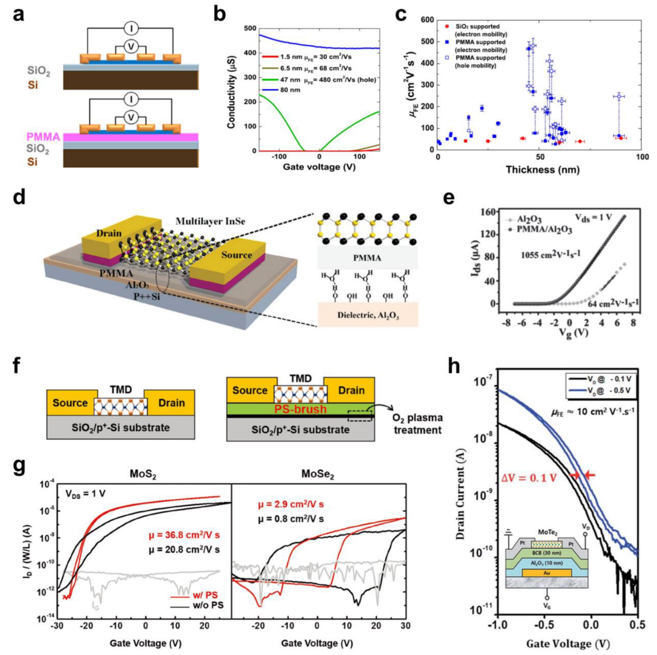
| 2D Material | Dielectric Layer | Processing Method for Polymer | Gate Structure | μ (cm2/Vs) | Operating Voltage (V) | Ref. |
|---|---|---|---|---|---|---|
| InSe | PMMA/Al2O3 | Spin-coating | Bottom gate | 1055 | 6 | [60] |
| MoS2 MoSe2 | PS-brush/Al2O3 | Spin-coating | Bottom gate | 20 1.8 | 9 5 | [61] |
| MoS2 MoTe2 | BCB/SiO2 | Spin-casting | Bottom gate | 15.8 18.2 | 40 | [62] |
| MoTe2 | BCB/Al2O3 | Spin-casting | Bottom gate | 10 | 1 | [62] |
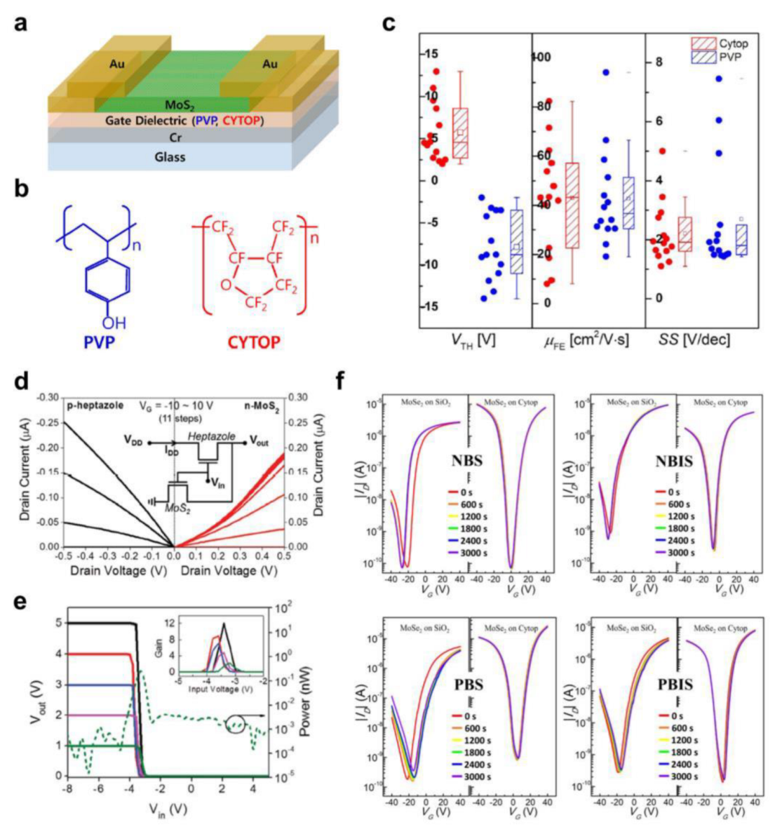
| MoS2 | CYTOP cPVP | Spin-coating | Bottom gate | 43.0 42.7 | 20 30 | [68] |
| 3L MoS2 10L MoS2 | CYTOP/Al2O3 | Spin-coating | Top gate | 6.0 14.9 | 10 | [39] |
| MoSe2 | CYTOP/SiO2 | Spin-coating | Bottom gate | 16.4 (hole) 18.4 (electron) | 40 | [69] |
| MoS2 | cPVP | Spin-coating | Bottom gate | 4.7 | 40 | [93] |
| MoS2 | Al2O3/SU-8 | Spin-coating | Bottom gate | 141.3 | 40 | [21] |
| Graphene | Parylene/SiO2 | CVD | Bottom gate | 10,600 (hole) 9800 (electron) | 60 | [95] |
| MoSe2 | Parylene/SiO2 | CVD | Bottom gate | 118 | 60 | [96] |
| WS2 | Parylene | N/A * | Bottom gate | 8.3 | 75 | [97] |
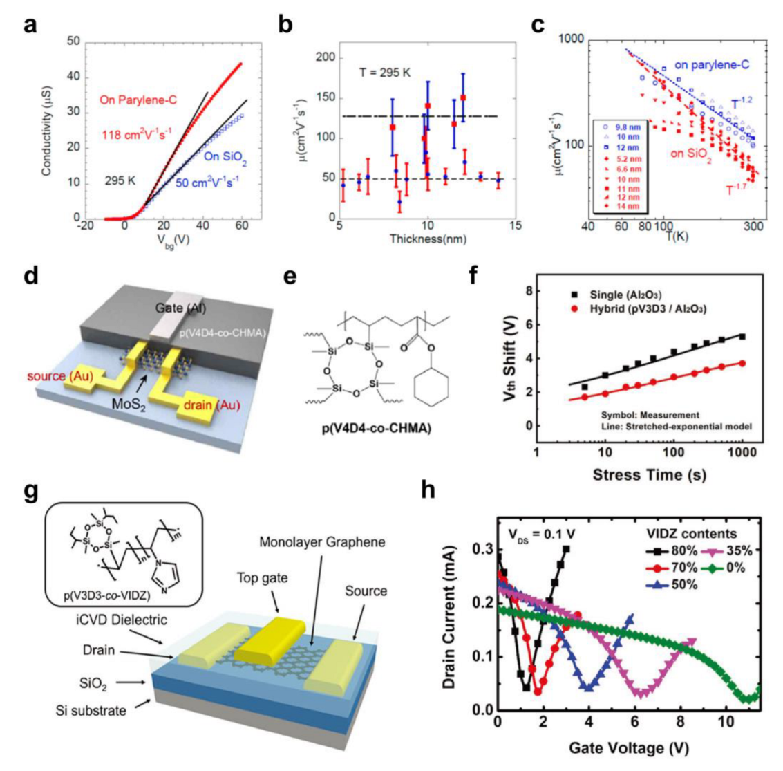
| MoS2 | P(V4D4-co-CHMA) | iCVD | Top gate | 35.1 | 5 | [106] |
| MoS2 | PV3D3/Al2O3 | iCVD | Bottom gate | 10.4 | 5 | [107] |
| Graphene | P(V3D3-co-VIDZ) | iCVD | Top gate | 7200 (hole) 3800 (electron) | 3 | [108] |
| 2D Material | Dielectric Layer | μ (cm2/Vs) | SS (mV/dec.) | Operating Voltage (V) | Applications | Ref. |
|---|---|---|---|---|---|---|
| MoS2 | P(VDF-TrFE) | 625 | N/A * | 30 | Ferroelectric memory | [121] |
| BP | P(VDF-TrFE) | 131~1159 | 900~3300 | 20 | Ferroelectric memory | [122] |
| WSe2 | P(VDF-TrFE) | 257 | N/A | 60 | Ferroelectric memory | [123] |
| Graphene | P(VDF-TrFE-CFE) | 3170 (hole) 1630 (electron) | N/A | 10 | Flexible FET | [124] |
| MoS2 | P(VDF-TrFE-CFE) | 51.9 | N/A | 10 | Photodetector | [125] |
| MoS2 | P(VDF-TrFE) | 86.5 | N/A | 40 | Photodetector | [126] |
| MoS2 | P(VDF-TrFE) | 220 | 300 | 20 | Ferroelectric memory | [127] |
| MoS2 | P(VDF-TrFE) | 175 | N/A | 20 | Ferroelectric memory | [129] |
| MoS2 | Al2O3/metal/P(VDF-TrFE) | N/A | 11.7 | 9 | NC-FET | [132] |
| MoS2 | P(VDF-TrFE) | N/A | 24.2 | 40 | NC-FET | [133] |
| MoS2 | HfO2/P(VDF-TrFE) | − | 37.2 | 3 | NC-FET | [134] |
Disclaimer/Publisher’s Note: The statements, opinions and data contained in all publications are solely those of the individual author(s) and contributor(s) and not of MDPI and/or the editor(s). MDPI and/or the editor(s) disclaim responsibility for any injury to people or property resulting from any ideas, methods, instructions or products referred to in the content. |
© 2023 by the authors. Licensee MDPI, Basel, Switzerland. This article is an open access article distributed under the terms and conditions of the Creative Commons Attribution (CC BY) license (https://creativecommons.org/licenses/by/4.0/).
Share and Cite
Choi, J.; Yoo, H. Combination of Polymer Gate Dielectric and Two-Dimensional Semiconductor for Emerging Field-Effect Transistors. Polymers 2023, 15, 1395. https://doi.org/10.3390/polym15061395
Choi J, Yoo H. Combination of Polymer Gate Dielectric and Two-Dimensional Semiconductor for Emerging Field-Effect Transistors. Polymers. 2023; 15(6):1395. https://doi.org/10.3390/polym15061395
Chicago/Turabian StyleChoi, Junhwan, and Hocheon Yoo. 2023. "Combination of Polymer Gate Dielectric and Two-Dimensional Semiconductor for Emerging Field-Effect Transistors" Polymers 15, no. 6: 1395. https://doi.org/10.3390/polym15061395