
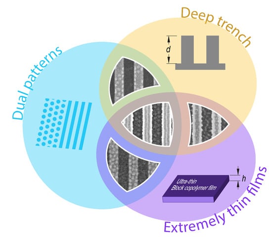
Non-Bulk Morphologies of Extremely Thin Block Copolymer Films Cast on Topographically Defined Substrates Featuring Deep Trenches: The Importance of Lateral Confinement


Abstract
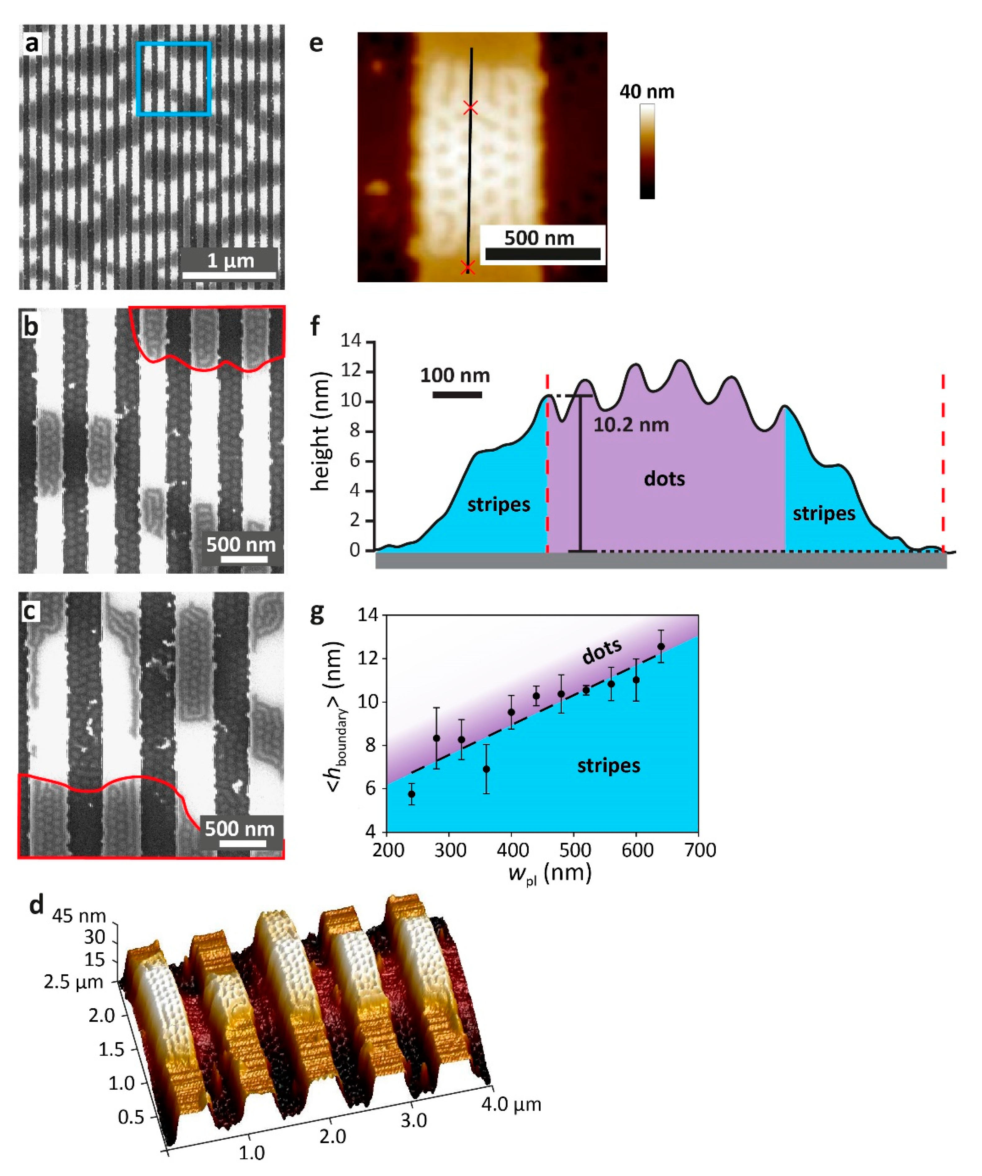
:
1. Introduction
2. Materials and Methods
3. Results and Discussion
4. Conclusions
Supplementary Materials
Author Contributions
Funding
Institutional Review Board Statement
Data Availability Statement
Acknowledgments
Conflicts of Interest
References
- Hamley, I.W. The Physics of Block Copolymers; Oxford University Press: Oxford, UK, 1998; p. 424. [Google Scholar]
- Bates, F.S.; Fredrickson, G.H. Block Copolymers—Designer Soft Materials. Phys. Today 1999, 52, 32–38. [Google Scholar] [CrossRef]
- Fasolka, M.J.; Mayes, A.M. Block Copolymer Thin Films: Physics and Applications. Annu. Rev. Mater. Res. 2001, 31, 323–355. [Google Scholar] [CrossRef] [Green Version]
- Hamley, I.W. Nanostructure Fabrication Using Block Copolymers. Nanotechnology 2003, 14, R39–R54. [Google Scholar] [CrossRef]
- Hu, H.Q.; Gopinadhan, M.; Osuji, C.O. Directed Self-Assembly of Block Copolymers: A Tutorial Review of Strategies for Enabling Nanotechnology with Soft Matter. Soft Matter 2014, 10, 3867–3889. [Google Scholar] [CrossRef]
- Cummins, C.; Lundy, R.; Walsh, J.J.; Ponsinet, V.; Fleury, G.; Morris, M.A. Enabling Future Nanomanufacturing through Block Copolymer Self-Assembly: A Review. Nano Today 2020, 35, 100936. [Google Scholar] [CrossRef]
- Segalman, R.A. Patterning with Block Copolymer Thin Films. Mater. Sci. Eng. R 2005, 48, 191–226. [Google Scholar] [CrossRef] [Green Version]
- Segal-Peretz, T.; Winterstein, J.; Doxastakis, M.; Ramirez-Hernandez, A.; Biswas, M.; Ren, J.X.; Suh, H.S.; Darling, S.B.; Liddle, J.A.; Elam, J.W.; et al. Characterizing the Three-Dimensional Structure of Block Copolymers Via Sequential Infiltration Synthesis and Scanning Transmission Electron Tomography. ACS Nano 2015, 9, 5333–5347. [Google Scholar] [CrossRef]
- Morris, M.A. Directed Self-Assembly of Block Copolymers for Nanocircuitry Fabrication. Microelectron. Eng. 2015, 132, 207–217. [Google Scholar] [CrossRef]
- Doerk, G.S.; Cheng, J.Y.; Singh, G.; Rettner, C.T.; Pitera, J.W.; Balakrishnan, S.; Arellano, N.; Sanders, D.P. Enabling Complex Nanoscale Pattern Customization Using Directed Self-Assembly. Nat. Commun. 2014, 5, 5805. [Google Scholar] [CrossRef] [Green Version]
- Shenhar, R.; Norsten, T.B.; Rotello, V.M. Polymer-Mediated Nanoparticle Assembly: Structural Control and Applications. Adv. Mater. 2005, 17, 657–669. [Google Scholar] [CrossRef]
- Bockstaller, M.R.; Mickiewicz, R.A.; Thomas, E.L. Block Copolymer Nanocomposites: Perspectives for Tailored Functional Materials. Adv. Mater. 2005, 17, 1331–1349. [Google Scholar] [CrossRef]
- Pavan, M.J.; Shenhar, R. Two-Dimensional Nanoparticle Organization Using Block Copolymer Thin Films as Templates. J. Mater. Chem. 2011, 21, 2028–2040. [Google Scholar] [CrossRef]
- Muzaffar-Kawasma, R.; Oded, M.; Shenhar, R. Assembly of Semiconductor Nanorods into Circular Arrangements Mediated by Block Copolymer Micelles. Materials 2022, 15, 2949. [Google Scholar] [CrossRef]
- Ploshnik, E.; Salant, A.; Banin, U.; Shenhar, R. Hierarchical Surface Patterns of Nanorods Obtained by Co-Assembly with Block Copolymers in Ultrathin Films. Adv. Mater. 2010, 22, 2774–2779. [Google Scholar] [CrossRef]
- Michman, E.; Shenhar, R. Directed Self-Assembly of Block Copolymer-Based Nanocomposites in Thin Films. Polym. Adv. Technol. 2017, 28, 613–622. [Google Scholar] [CrossRef]
- Onses, M.S.; Thode, C.J.; Liu, C.-C.; Ji, S.; Cook, P.L.; Himpsel, F.J.; Nealey, P.F. Site-Specific Placement of Au Nanoparticles on Chemical Nanopatterns Prepared by Molecular Transfer Printing Using Block-Copolymer Films. Adv. Funct. Mater. 2011, 21, 3074–3082. [Google Scholar] [CrossRef]
- Kang, H.; Detcheverry, F.A.; Mangham, A.N.; Stoykovich, M.P.; Daoulas, K.C.; Hamers, R.J.; Mueller, M.; de Pablo, J.J.; Nealey, P.F. Hierarchical Assembly of Nanoparticle Superstructures from Block Copolymer-Nanoparticle Composites. Phys. Rev. Lett. 2008, 100, 148303. [Google Scholar] [CrossRef]
- Shin, D.O.; Mun, J.H.; Hwang, G.-T.; Yoon, J.M.; Kim, J.Y.; Yun, J.M.; Yang, Y.-B.; Oh, Y.; Lee, J.Y.; Shin, J.; et al. Multicomponent Nanopatterns by Directed Block Copolymer Self-Assembly. ACS Nano 2013, 7, 8899–8907. [Google Scholar] [CrossRef]
- Schelhas, L.T.; Farrell, R.A.; Halim, U.; Tolbert, S.H. Directed Self-Assembly as a Route to Ferromagnetic and Superparamagnetic Nanoparticle Arrays. Adv. Funct. Mater. 2014, 24, 6956–6962. [Google Scholar] [CrossRef]
- Olson, D.A.; Chen, L.; Hillmyer, M.A. Templating Nanoporous Polymers with Ordered Block Copolymers. Chem. Mater. 2008, 20, 869–890. [Google Scholar] [CrossRef]
- Jackson, E.A.; Hillmyer, M.A. Nanoporous Membranes Derived from Block Copolymers: From Drug Delivery to Water Filtration. ACS Nano 2010, 4, 3548–3553. [Google Scholar] [CrossRef] [PubMed]
- Phillip, W.A.; O’Neill, B.; Rodwogin, M.; Hillmyer, M.A.; Cussler, E.L. Self-Assembled Block Copolymer Thin Films as Water Filtration Membranes. ACS Appl. Mater. Interfaces 2010, 2, 847–853. [Google Scholar] [CrossRef] [PubMed]
- Yang, S.Y.; Ryu, I.; Kim, H.Y.; Kim, J.K.; Jang, S.K.; Russell, T.P. Nanoporous Membranes with Ultrahigh Selectivity and Flux for the Filtration of Viruses. Adv. Mater. 2006, 18, 709–712. [Google Scholar] [CrossRef]
- Zhou, C.; Segal-Peretz, T.; Oruc, M.E.; Suh, H.S.; Wu, G.P.; Nealey, P.F. Fabrication of Nanoporous Alumina Ultrafiltration Membrane with Tunable Pore Size Using Block Copolymer Templates. Adv. Funct. Mater. 2017, 27, 1701756. [Google Scholar] [CrossRef]
- Jung, Y.S.; Jung, W.; Tuller, H.L.; Ross, C.A. Nanowire Conductive Polymer Gas Sensor Patterned Using Self-Assembled Block Copolymer Lithography. Nano Lett. 2008, 8, 3776–3780. [Google Scholar] [CrossRef]
- Shen, M.Y.; Yuran, S.; Aviv, Y.; Ayalew, H.; Luo, C.H.; Tsai, Y.H.; Reches, M.; Yu, H.H.; Shenhar, R. Electrically Responsive, Nanopatterned Surfaces for Triggered Delivery of Biologically Active Molecules into Cells. ACS Appl. Mater. Interfaces 2019, 11, 1201–1208. [Google Scholar] [CrossRef]
- Otsuka, H.; Nagasaki, Y.; Kataoka, K. Self-Assembly of Poly(Ethylene Glycol)-Based Block Copolymers for Biomedical Applications. Curr. Opin. Colloid Interface Sci. 2001, 6, 3–10. [Google Scholar] [CrossRef]
- Takenaka, M.; Hasegawa, H. Directed Self-Assembly of Block Copolymers. Curr. Opin. Chem. Eng. 2013, 2, 88–94. [Google Scholar] [CrossRef] [Green Version]
- Jeong, S.J.; Kim, J.Y.; Kim, B.H.; Moon, H.S.; Kim, S.O. Directed Self-Assembly of Block Copolymers for Next Generation Nanolithography. Mater. Today 2013, 16, 468–476. [Google Scholar] [CrossRef]
- Koo, K.; Ahn, H.; Kim, S.W.; Ryu, D.Y.; Russell, T.P. Directed Self-Assembly of Block Copolymers in the Extreme: Guiding Microdomains from the Small to the Large. Soft Matter 2013, 9, 9059–9071. [Google Scholar] [CrossRef]
- Darling, S.B. Directing the Self-Assembly of Block Copolymers. Prog. Polym. Sci. 2007, 32, 1152–1204. [Google Scholar] [CrossRef]
- Rockford, L.; Liu, Y.; Mansky, P.; Russell, T.P.; Yoon, M.; Mochrie, S.G.J. Polymers on Nanoperiodic, Heterogeneous Surfaces. Phys. Rev. Lett. 1999, 82, 2602–2605. [Google Scholar] [CrossRef] [Green Version]
- Segalman, R.A.; Yokoyama, H.; Kramer, E.J. Graphoepitaxy of Spherical Domain Block Copolymer Films. Adv. Mater. 2001, 13, 1152–1155. [Google Scholar] [CrossRef]
- Kim, S.O.; Solak, H.H.; Stoykovich, M.P.; Ferrier, N.J.; de Pablo, J.J.; Nealey, P.F. Epitaxial Self-Assembly of Block Copolymers on Lithographically Defined Nanopatterned Substrates. Nature 2003, 424, 411–414. [Google Scholar] [CrossRef]
- Sundrani, D.; Darling, S.B.; Sibener, S.J. Guiding Polymers to Perfection: Macroscopic Alignment of Nanoscale Domains. Nano Lett. 2004, 4, 273–276. [Google Scholar] [CrossRef]
- Cheng, J.Y.; Mayes, A.M.; Ross, C.A. Nanostructure Engineering by Templated Self-Assembly of Block Copolymers. Nat. Mater. 2004, 3, 823–828. [Google Scholar] [CrossRef]
- Bita, I.; Yang, J.K.W.; Jung, Y.S.; Ross, C.A.; Thomas, E.L.; Berggren, K.K. Graphoepitaxy of Self-Assembled Block Copolymers on Two-Dimensional Periodic Patterned Templates. Science 2008, 321, 939–943. [Google Scholar] [CrossRef] [Green Version]
- Ruiz, R.; Kang, H.; Detcheverry, F.A.; Dobisz, E.; Kercher, D.S.; Albrecht, T.R.; de Pablo, J.J.; Nealey, P.F. Density Multiplication and Improved Lithography by Directed Block Copolymer Assembly. Science 2008, 321, 936–939. [Google Scholar] [CrossRef]
- Chang, T.H.; Xiong, S.S.; Liu, C.C.; Liu, D.; Nealey, P.F.; Ma, Z.Q. The One-Pot Directed Assembly of Cylinder-Forming Block Copolymer on Adjacent Chemical Patterns for Bimodal Patterning. Macromol. Rapid Commun. 2017, 38, 1700285. [Google Scholar] [CrossRef] [Green Version]
- Stein, A.; Wright, G.; Yager, K.G.; Doerk, G.S.; Black, C.T. Selective Directed Self-Assembly of Coexisting Morphologies Using Block Copolymer Blends. Nat. Commun. 2016, 7, 12366. [Google Scholar] [CrossRef]
- Cheng, J.Y.; Ross, C.A.; Smith, H.I.; Thomas, E.L. Templated Self-Assembly of Block Copolymers: Top-Down Helps Bottom-Up. Adv. Mater. 2006, 18, 2505–2521. [Google Scholar] [CrossRef]
- Yang, J.K.W.; Jung, Y.S.; Chang, J.-B.; Mickiewicz, R.A.; Alexander-Katz, A.; Ross, C.A.; Berggren, K.K. Complex Self-Assembled Patterns Using Sparse Commensurate Templates with Locally Varying Motifs. Nat. Nanotechnol. 2010, 5, 256–260. [Google Scholar] [CrossRef] [PubMed]
- Chang, J.-B.; Choi, H.K.; Hannon, A.F.; Alexander-Katz, A.; Ross, C.A.; Berggren, K.K. Design Rules for Self-Assembled Block Copolymer Patterns Using Tiled Templates. Nat. Commun. 2014, 5, 3305. [Google Scholar] [CrossRef] [PubMed] [Green Version]
- Hannon, A.F.; Ding, Y.; Bai, W.B.; Ross, C.A.; Alexander-Katz, A. Optimizing Topographical Templates for Directed Self-Assembly of Block Copolymers Via Inverse Design Simulations. Nano Lett. 2014, 14, 318–325. [Google Scholar] [CrossRef]
- Tavakkoli, A.K.G.; Gotrik, K.W.; Hannon, A.F.; Alexander-Katz, A.; Ross, C.A.; Berggren, K.K. Templating Three-Dimensional Self-Assembled Structures in Bilayer Block Copolymer Films. Science 2012, 336, 1294–1298. [Google Scholar] [CrossRef]
- Tavakkoli, A.K.G.; Nicaise, S.M.; Hannon, A.F.; Gotrik, K.W.; Alexander-Katz, A.; Ross, C.A.; Berggren, K.K. Sacrificial-Post Templating Method for Block Copolymer Self-Assembly. Small 2014, 10, 493–499. [Google Scholar] [CrossRef] [Green Version]
- Tavakkoli, A.K.G.; Nicaise, S.M.; Gadelrab, K.R.; Alexander-Katz, A.; Ross, C.A.; Berggren, K.K. Multilayer Block Copolymer Meshes by Orthogonal Self-Assembly. Nat. Commun. 2016, 7, 10518. [Google Scholar] [CrossRef] [Green Version]
- Liu, R.Z.; Huang, H.J.; Sun, Z.H.; Alexander-Katz, A.; Ross, C.A. Metallic Nanomeshes Fabricated by Multimechanism Directed Self-Assembly. ACS Nano 2021, 15, 16266–16276. [Google Scholar] [CrossRef]
- Chai, J.; Buriak, J.M. Using Cylindrical Domains of Block Copolymers to Self-Assemble and Align Metallic Nanowires. ACS Nano 2008, 2, 489–501. [Google Scholar] [CrossRef]
- Jin, C.; Olsen, B.C.; Luber, E.J.; Buriak, J.M. Preferential Alignment of Incommensurate Block Copolymer Dot Arrays Forming Moire Superstructures. ACS Nano 2017, 11, 3237–3246. [Google Scholar] [CrossRef] [Green Version]
- Cha, S.K.; Yong, D.; Yang, G.G.; Jin, H.M.; Kim, J.H.; Han, K.H.; Kim, J.U.; Jeong, S.-J.; Kim, S.O. Nanopatterns with a Square Symmetry from an Orthogonal Lamellar Assembly of Block Copolymers. ACS Appl. Mater. Interfaces 2019, 11, 20265–20271. [Google Scholar] [CrossRef]
- Stoykovich, M.P.; Müller, M.; Kim, S.O.; Solak, H.H.; Edwards, E.W.; de Pablo, J.J.; Nealey, P.F. Directed Assembly of Block Copolymer Blends into Nonregular Device-Oriented Structures. Science 2005, 308, 1442–1446. [Google Scholar] [CrossRef] [Green Version]
- Stoykovich, M.P.; Kang, H.; Daoulas, K.C.; Liu, G.; Liu, C.-C.; de Pablo, J.J.; Mueller, M.; Nealey, P.F. Directed Self-Assembly of Block Copolymers for Nanolithography: Fabrication of Isolated Features and Essential Integrated Circuit Geometries. ACS Nano 2007, 1, 168–175. [Google Scholar] [CrossRef]
- Liu, G.; Thomas, C.S.; Craig, G.S.W.; Nealey, P.F. Integration of Density Multiplication in the Formation of Device-Oriented Structures by Directed Assembly of Block Copolymer-Homopolymer Blends. Adv. Funct. Mater. 2010, 20, 1251–1257. [Google Scholar] [CrossRef]
- Zhao, W.; Li, W. Hybrid Patterns from Directed Self-Assembly of Diblock Copolymers by Chemical Patterns. Phys. Chem. Chem. Phys. 2019, 21, 18525–18532. [Google Scholar] [CrossRef]
- Zhao, W.; Duan, C.; Li, W. Hybrid Line-Dot Nanopatterns from Directed Self-Assembly of Diblock Copolymers by Trenches. Phys. Chem. Chem. Phys. 2019, 21, 10011–10021. [Google Scholar] [CrossRef]
- Herr, D.J.C. Directed Block Copolymer Self-Assembly for Nanoelectronics Fabrication. J. Mater. Res. 2011, 26, 122–139. [Google Scholar] [CrossRef]
- Stefik, M.; Guldin, S.; Vignolini, S.; Wiesner, U.; Steiner, U. Block Copolymer Self-Assembly for Nanophotonics. Chem. Soc. Rev. 2015, 44, 5076–5091. [Google Scholar] [CrossRef] [Green Version]
- Bates, C.M.; Bates, F.S. 50th Anniversary Perspective: Block Polymers-Pure Potential. Macromolecules 2017, 50, 3–22. [Google Scholar] [CrossRef]
- Hawker, C.J.; Russell, T.P. Block Copolymer Lithography: Merging “Bottom-up” with “Top-Down” Processes. MRS Bull. 2005, 30, 952–966. [Google Scholar] [CrossRef] [Green Version]
- Li, W.; Mueller, M. Directed Self-Assembly of Block Copolymers by Chemical or Topographical Guiding Patterns: Optimizing Molecular Architecture, Thin-Film Properties, and Kinetics. Prog. Polym. Sci. 2016, 54–55, 47–75. [Google Scholar] [CrossRef]
- Luo, M.; Epps, T.H. Directed Block Copolymer Thin Film Self-Assembly: Emerging Trends in Nanopattern Fabrication. Macromolecules 2013, 46, 7567–7579. [Google Scholar] [CrossRef]
- Park, C.; Yoon, J.; Thomas, E.L. Enabling Nanotechnology with Self Assembled Block Copolymer Patterns. Polymer 2003, 44, 6725–6760. [Google Scholar] [CrossRef] [Green Version]
- Doerk, G.S.; Yager, K.G. Beyond Native Block Copolymer Morphologies. Mol. Syst. Des. Eng. 2017, 2, 518–538. [Google Scholar] [CrossRef]
- Cheng, J.Y.; Rettner, C.T.; Sanders, D.P.; Kim, H.C.; Hinsberg, W.D. Dense Self-Assembly on Sparse Chemical Patterns: Rectifying and Multiplying Lithographic Patterns Using Block Copolymers. Adv. Mater. 2008, 20, 3155–3158. [Google Scholar] [CrossRef]
- Ji, S.; Wan, L.; Liu, C.-C.; Nealey, P.F. Directed Self-Assembly of Block Copolymers on Chemical Patterns: A Platform for Nanofabrication. Prog. Polym. Sci. 2016, 54–55, 76–127. [Google Scholar] [CrossRef]
- Liu, C.-C.; Ramirez-Hernandez, A.; Han, E.; Craig, G.S.W.; Tada, Y.; Yoshida, H.; Kang, H.; Ji, S.; Gopalan, P.; de Pablo, J.J.; et al. Chemical Patterns for Directed Self-Assembly of Lamellae-Forming Block Copolymers with Density Multiplication of Features. Macromolecules 2013, 46, 1415–1424. [Google Scholar] [CrossRef]
- Pinto-Gomez, C.; Perez-Murano, F.; Bausells, J.; Villanueva, L.G.; Fernandez-Regulez, M. Directed Self-Assembly of Block Copolymers for the Fabrication of Functional Devices. Polymers 2020, 12, 2432. [Google Scholar] [CrossRef]
- Brassat, K.; Kool, D.; Nallet, C.G.A.; Lindner, J.K.N. Understanding Film Thickness-Dependent Block Copolymer Self-Assembly by Controlled Polymer Dewetting on Prepatterned Surfaces. Adv. Mater. Interfaces 2020, 7, 1901605. [Google Scholar] [CrossRef]
- Michman, E.; Langenberg, M.; Stenger, R.; Oded, M.; Schvartzman, M.; Müller, M.; Shenhar, R. Controlled Spacing between Nanopatterned Regions in Block Copolymer Films Obtained by Utilizing Substrate Topography for Local Film Thickness Differentiation. ACS Appl. Mater. Interfaces 2019, 11, 35247–35254. [Google Scholar] [CrossRef]
- Knoll, A.; Horvat, A.; Lyakhova, K.S.; Krausch, G.; Sevink, G.J.A.; Zvelindovsky, A.V.; Magerle, R. Phase Behavior in Thin Films of Cylinder-Forming Block Copolymers. Phys. Rev. Lett. 2002, 89, 035501. [Google Scholar] [CrossRef]
- Shin, J.Y.; Oh, Y.T.; Kim, S.; Lim, H.Y.; Lee, B.; Ko, Y.C.; Park, S.; Seon, S.W.; Lee, S.G.; Mun, S.S.; et al. Hierarchical Self-Assembly of Thickness-Modulated Block Copolymer Thin Films for Controlling Nanodomain Orientations inside Bare Silicon Trenches. Polymers 2021, 13, 553. [Google Scholar] [CrossRef]
- Michman, E.; Oded, M.; Shenhar, R. Dual Block Copolymer Morphologies in Ultrathin Films on Topographic Substrates: The Effect of Film Curvature. Polymers 2022, 14, 2377. [Google Scholar] [CrossRef]
- Halevi, A.; Halivni, S.; Oded, M.; Mueller, A.H.E.; Banin, U.; Shenhar, R. Co-Assembly of A-B Diblock Copolymers with B’-Type Nanoparticles in Thin Films: Effect of Copolymer Composition and Nanoparticle Shape. Macromolecules 2014, 47, 3022–3032. [Google Scholar] [CrossRef]
- Decoster, S.; Piao, X.Y.; Gillijns, W.; Lazzarino, F. Modeling the Topography of Uneven Substrates Post Spin-Coating. J. Vac. Sci. Technol. B 2018, 36, 03E102. [Google Scholar] [CrossRef]
- Lang, C.I.; Boning, D.S. Modeling Spin Coating over Topography and Uniformity Improvements through Fill Patterns for Advanced Packaging Technologies. IEEE Trans. Semicond. Manuf. 2019, 32, 62–69. [Google Scholar] [CrossRef]
- Hanakata, P.Z.; Betancourt, B.A.P.; Douglas, J.F.; Starr, F.W. A Unifying Framework to Quantify the Effects of Substrate Interactions, Stiffness, and Roughness on the Dynamics of Thin Supported Polymer Films. J. Chem. Phys. 2015, 142, 234907. [Google Scholar] [CrossRef]
- Unni, A.B.; Chat, K.; Duarte, D.M.; Wojtyniak, M.; Geppert-Rybczynska, M.; Kubacki, J.; Wrzalik, R.; Richert, R.; Adrjanowicz, K. Experimental Evidence on the Effect of Substrate Roughness on Segmental Dynamics of Confined Polymer Films. Polymer 2020, 199, 122501. [Google Scholar] [CrossRef]
- Ham, S.; Shin, C.; Kim, E.; Ryu, D.Y.; Jeong, U.; Russell, T.P.; Hawker, C.J. Microdomain Orientation of PS-b-PMMA by Controlled Interfacial Interactions. Macromolecules 2008, 41, 6431–6437. [Google Scholar] [CrossRef]
- Choi, S.Y.; Lee, C.; Lee, J.W.; Park, C.; Kim, S.H. Dewetting-Induced Hierarchical Patterns in Block Copolymer Films. Macromolecules 2012, 45, 1492–1498. [Google Scholar] [CrossRef]
- Eren, N.; Burg, O.; Michman, E.; Popov, I.; Shenhar, R. Gold Nanoparticle Arrays Organized in Mixed Patterns through Directed Self-Assembly of Ultrathin Block Copolymer Films on Topographic Substrates. Polymer 2022, 245, 124727. [Google Scholar] [CrossRef]
- Xuan, Y.; Peng, J.; Cui, L.; Wang, H.F.; Li, B.Y.; Han, Y.C. Morphology Development of Ultrathin Symmetric Diblock Copolymer Film Via Solvent Vapor Treatment. Macromolecules 2004, 37, 7301–7307. [Google Scholar] [CrossRef]


Disclaimer/Publisher’s Note: The statements, opinions and data contained in all publications are solely those of the individual author(s) and contributor(s) and not of MDPI and/or the editor(s). MDPI and/or the editor(s) disclaim responsibility for any injury to people or property resulting from any ideas, methods, instructions or products referred to in the content. |
© 2023 by the authors. Licensee MDPI, Basel, Switzerland. This article is an open access article distributed under the terms and conditions of the Creative Commons Attribution (CC BY) license (https://creativecommons.org/licenses/by/4.0/).
Share and Cite
Michman, E.; Oded, M.; Shenhar, R. Non-Bulk Morphologies of Extremely Thin Block Copolymer Films Cast on Topographically Defined Substrates Featuring Deep Trenches: The Importance of Lateral Confinement. Polymers 2023, 15, 1035. https://doi.org/10.3390/polym15041035
Michman E, Oded M, Shenhar R. Non-Bulk Morphologies of Extremely Thin Block Copolymer Films Cast on Topographically Defined Substrates Featuring Deep Trenches: The Importance of Lateral Confinement. Polymers. 2023; 15(4):1035. https://doi.org/10.3390/polym15041035
Chicago/Turabian StyleMichman, Elisheva, Meirav Oded, and Roy Shenhar. 2023. "Non-Bulk Morphologies of Extremely Thin Block Copolymer Films Cast on Topographically Defined Substrates Featuring Deep Trenches: The Importance of Lateral Confinement" Polymers 15, no. 4: 1035. https://doi.org/10.3390/polym15041035